Abstract
We report on demonstrating high performance lateral β-Ga2O3 metal-oxide-semiconductor field-effect transistors (MOSFETs) with source-connected field plate (FP) on a thin (150 nm) and highly Si-doped (n = 1.5 × 1018 cm−3) β-Ga2O3 epitaxial channel layer grown by ozone molecular beam epitaxy (MBE) on Fe-doped semi-insulating (010) substrate. For a MOSFET with a gate-drain spacing (Lgd) of 25 μm, the three terminal off-state breakdown voltage (VBR) tested in Fluorinert ambient reaches 2321 V. To the best of our knowledge, this is the first report of lateral β-Ga2O3 MOSFET with high VBR of more than 2 kV and the highest VBR attained among all the Ga2O3 MOSFETs. The breakdown voltages with different Lgd from 5–25 μm ranged from 518–2321V, with a linear trend of increasing breakdown voltage for larger spacing lateral MOSFETs. Combining with high electrical performances and excellent material properties, source-connected FP lateral β-Ga2O3 MOSFET implies its great potential for next generation high-voltage and high-power switching devices applications above 2 kV.
Export citation and abstract BibTeX RIS

This is an open access article distributed under the terms of the Creative Commons Attribution 4.0 License (CC BY, http://creativecommons.org/licenses/by/4.0/), which permits unrestricted reuse of the work in any medium, provided the original work is properly cited.
Although gallium oxide (Ga2O3) exists as different phases of α, β, δ, γ, and ɛ under various thermodynamic conditions, monoclinic β-Ga2O3 is the most stable form with a wide bandgap up to 4.9 eV1 and a high expected breakdown electric field (EBR) of about 6–8 MV/cm.2 Thanks to its ultra-wide bandgap (UWBG), it has a wide potential for high electric field,3–5 high temperature,6,7 and UV optoelectronics applications.8,9 Among these advantages of β-Ga2O3, the high breakdown electric field (EBR) is the most attractive property. Because the Baliga's figure-of-merit (FOM), which is the basic parameter to evaluate how suitable a semiconductor is for power devices, is proportional to EBR3, but is only linearly proportional to the mobility (μ). As compared to GaN and SiC, the conduction loss of β-Ga2O3 power devices can be one order of magnitude lower at the same breakdown voltage (VBR). Moreover, high quality β-Ga2O3 wafers can be manufactured in large volumes by scalable low cost melt-growth techniques.10 For these reasons, β-Ga2O3 is very attractive to use in high-voltage and high-power switching electronics applications such as renewable energy, electric vehicles, defense electronics and power conditioning in large industrial motors.11,12
A few high performance Ga2O3 power devices have been reported in recent years. They include a vertical Schottky barrier diode (SBD) with high VBR of 2.3 kV,12 a record high FP lateral SBD with more than 3 kV VBR,13 a high cutoff frequency and maximum oscillation frequency (fT/fmax) of 3.3/12.9 GHz14 and a record high breakdown field of 3.8 MV/cm3 and later 5.2 MV/cm.4 Following the first demonstration of Ga2O3 MOSFET with three-terminal off-state VBR of 370V in 2013,15 a VBR of 382 V with selective SOG doping of source and drain,16 a recessed enhanced-mode MOSFET with VBR of 505 V,17 a FP lateral MOSFET with high VBR of 755 kV,18 a vertical MOSFET with high VBR of 1 kV,19 and a record high lateral MOSFETs with 1.85 kV VBR by adopting gate-connected field plate and composite dielectrics layers20 have been reported.
In this work, we report a lateral β-Ga2O3 MOSFET with source-connected field plate with a record high VBR of 2321 V. A thin (150 nm) and highly Si-doped (1.5 × 1018 cm−3) β-Ga2O3 epitaxial channel layer grown by ozone MBE on Fe-doped semi-insulating (010) β-Ga2O3 bulk substrate can achieve the highest experimentally reported VBR in lateral β-Ga2O3 FP-MOSFETs. For this device, the EBR is calculated to be 0.93 MV/cm.
Experimental
Most electrical parameters such as pinch-off voltage (Vp), specific on-resistance (Ron,sp.), Ion/Ioff ratio, current density (A/mm) and VBR of the power MOSFETs are mainly determined by the channel design. Since this is our first device process, we have intuitively determined the epitaxial layer growth method and channel layer design based on the experience of the gallium arsenide (GaAs) power metal-semiconductor field-effect transistors (MESFETs). First, Fe-doped semi-insulating (010) β-Ga2O3 substrate and ozone MBE method were used to reduce substrate leakage current during operation of high power MOSFETs and increase the controllability of growth parameters of Si-doped thin β-Ga2O3 homoepitaxial channel layer.
In the channel design, we increased the doping concentration to order of 1018 cm−3 to form ohmic contacts without additional process, such as selective ion implantation with annealing and epitaxial layer regrowth with etching, at source and drain regions to improve ohmic contact properties. On the other hand, the channel layer thickness was reduced to much thinner than those of previous reported devices to decrease the pinch-off voltage of the device. The channel layer thickness (150 nm) and Si donor concentration (1.5 × 1018 cm−3) were verified by electrochemical capacitance-voltage (ECV) measurement as-grown at Novel Crystal in Japan. The Fe-doped semi-insulating (010) substrates used for epitaxial growth were grown by the edge-defined, film fed growth (EFG) method. At the current technology level, the maximum available wafer size is 10 mm × 15 mm and used for device fabrication in this work.
The device fabrication began with a custom-made epi wafer and a monitor of unintentionally doped (UID) Ga2O3 piece with same size. A 20 nm Al2O3 dielectric was deposited on the Ga2O3 free surface before starting process to keep original clean surface as-grown by plasm-enhanced atomic layer deposition (PEALD) at 300°C, which served as both the gate dielectric and channel pre-passivation. Device isolation was carried out with an inductively coupled plasma (ICP) reactive ion etch (RIE) using BCl3/N2 mixed gas chemistry. The composition of mixed etch gas was 12.5% N2 in BCl3 and the chamber pressure was fixed at 5 mTorr. The RF bias power was adjusted as low as 10% of ICP coil power to reduce plasma particle damage. Under these conditions, the mesa etched angle was about 150 degree, which was suitable for removing disconnection issue of metal lines that cross over the mesa etched channel region. Al2O3 layer in the source and drain regions was removed for ohmic metal contact to Ga2O3 using buffered oxide solution. Then source-drain ohmic contacts of the transistor were formed by depositing a Ti/Au (25/300 nm) metal layer using an E-beam evaporator and then annealing for 1 minute at 475°C in a nitrogen (N2) ambient. Circular transmission line method (C-TLM) was used to evaluate metal-semiconductor ohmic contact property. Unlike expectations, specific contact resistivity (ρc) was as high as 6.0 × 10⁻³ Ω⋅cm2. So, selective ion implantation and/or epitaxial regrowth process will be tried to improve ohmic contact properties in the next process.
After gate patterning and wafer cleaning with diluted HCl solution, the sample was deposited using a Ti/Au (25/300 nm) metal stack at pressure < 1 × 10⁻⁷ Torr. The gate-connected, source-connected, and drain-connected field plates are already well known as FP technologies in lateral GaN-based RF and power devices to increase their breakdown voltages. In particular, at low frequencies, the source-connected FP is more suitable for increasing the uniformity of the electric field profile across gate region and lowering peak electric field at the drain-side edge of the gate in the lateral GaN/AlGaN HEMTs. Because this characteristic might reduce the probability of breakdown at weaker points of the device, a source-connected FP structure, which is different from those of the previous reports, was applied in this work. Source-connected FP length (LFP) was designed to be 3 μm.
After checking the basic device characteristics, a 300 nm SiO2 field-plate dielectric film was grown by plasm-enhanced chemical vapor deposition (PECVD) at 300°C. This dielectric was used to serve a dual functionality for field-plate mechanical support as well as device surface passivation including mesa etched area. The dielectric via holes were formed by a CF4-based ICP RIE method and then a thick Ti/Au (20/450 nm) field plate metal was deposited for facilitating pad probing during measurement and reducing electrical resistance of the devices. Finally, all the devices were passivated with a 200nm Si3N4 dielectric layer by PECVD and then probing pads were opened by ICP RIE.
A cross-sectional view of β-Ga2O3 MOSFET with source-connected FP and MBE-grown epitaxial layers used in this work is shown in Fig. 1a. Three different dielectric films of Al2O3, SiO2, and Si3N4 are used for the high voltage device fabrication. The uppermost layer (dark green) of 200 nm Si3N4 film is used for final passivation and its description is not shown in this figure. Fig. 1b shows an optical microscope of finger-type MOSFET taken after gate electrode formation and basic d.c. parameter measurements. Fig. 1c shows a top-down SEM image of a lateral MOSFET with source-connected FP structure cross-over the gate finger. This corresponds to the region indicated by the dotted line in Fig. 1b. Device parameters are unit gate width (Wg) of 100 μm, gate length (Lg) of 3 μm, field plate length (LFP) of 3 μm, and gate-drain spacing (Lgd) of 5, 10, 15, 20, and 25 μm. Fig. 1d shows cross-sectional SEM view of the source, gate, drain and FP shapes of a source-connected FP-MOSFET with Lg = 3 μm, LFP = 3 μm, and Lgd = 15 μm, obtained from the focused ion beam (FIB) analysis. The Lgd and LFP, which mainly affect the breakdown voltage of the device, are formed about 14 μm (∼1 μm narrow) and about 3.3 μm (∼10% larger), respectively. Since the real Lgd value of the device was narrower than that of the designed one, if the EBR calculation is performed based on actual Lgd, the EBR values will be higher than those shown in Fig. 4. Therefore, the designed values are used for convenience of calculation of the EBR with the Lgd of MOSFETs in this work.
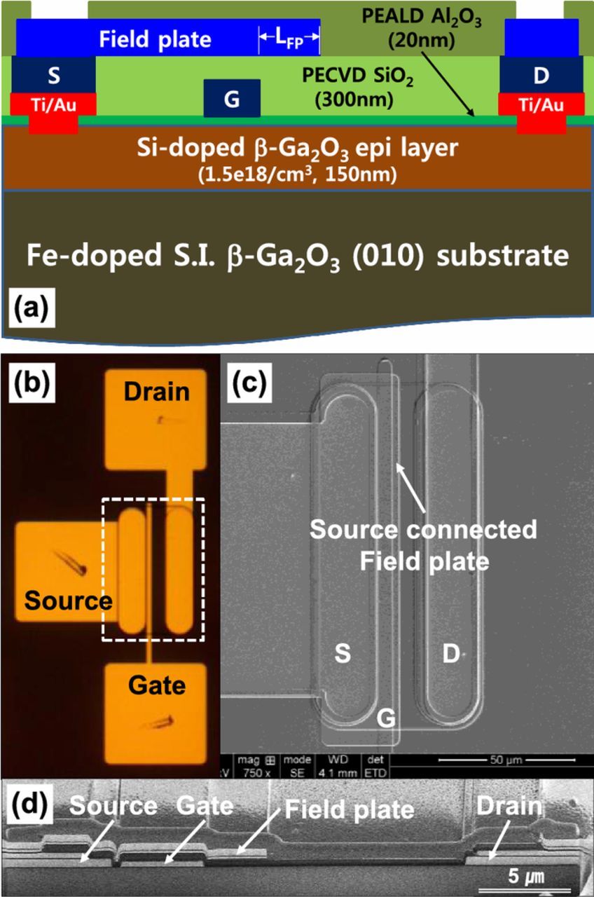
Figure 1. (a) Cross-section view of FP β-Ga2O3 MOSFET illustrating the structure of a source-connected FP. (b) Optical microscope of finger-type MOSFET taken after gate electrode formation and basic d.c. parameter measurements. (c) Top-down SEM image and (d) Cross-sectional SEM view of source-connected FP-MOSFET.
Results and Discussion
DC output current-voltage (I-V) characteristics of the fabricated source-connected FP-MOSFET with Lg = 3 μm, LFP = 3 μm, and Lgd = 25 μm were measured with an HP 4156B semiconductor parameter analyzer on a Cascade probe station at room temperature under air atmosphere conditions and shown in Fig. 2. Fig. 2a shows DC output family curves from Vgs = + 1 V to Vgs = −7 V with a gate voltage step of −1V. Fig. 2b and Fig. 2c show semi-log and linear scale transfer characteristics measured from Vgs = + 3 V to Vgs = −15 V with a gate voltage step of −0.05 V and at a constant VDS = 30 V, respectively. The Ion/Ioff ratio was estimated as high as 107. The pinch-off voltage, which is defined by a drain current density of 100 nA/mm,3 is typically observed around −4.6 V. The device shows a peak gm of 2.55 mS/mm at Vgs = + 1.3 V. The drain current density at Vgs = + 3 V and VDS = 30 V is typically around 10 mA/mm, as shown in Fig. 2b and Fig. 2c.
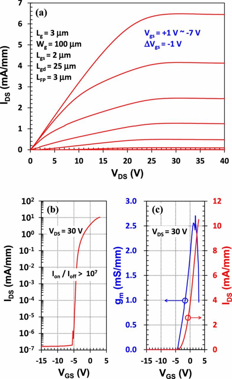
Figure 2. (a) DC Output current-voltage characteristics of the fabricated FP MOSFET with Lgd = 25 μm. (b) and (c) are semi-log and linear scale transfer characteristics measured at VDS = 30 V, along with the extracted Ion/Ioff ratio over 107.
The three-terminal off-state breakdown characteristics were measured with a Keithley Tektronix 371A High Power Curve Tracer. For the breakdown measurements, the devices were submerged in Fluorinert FC-770 to reduce air breakdown potential. Before breakdown test, we checked the leakage current level of the devices at VGS = −10V and VDS = + 30 V conditions. All leakage current levels of drain and gate were lower than 1.5 × 10⁻⁸ A. The system compliance was adjusted to 10 μA (∼ × 1000 higher than original leakage current) based on our own reference to protect the system during the catastrophic breakdown of the device and this value was used as a device breakdown criteria. The drain voltage was swept from 0 V to 3 kV with a voltage step of 2 V at a constant Vgs = −10 V. For a device with Lgd = 25 μm, the catastrophic breakdown was occurred at 2321 V as shown in Fig. 3a. This is the highest record of VBR measured in a lateral FP Ga2O3 MOSFET to date. The VBR for Lgd = 5 μm, 10 μm, and 20 μm were also measured with the same criteria of 10 μA and shown with Lgd = 25 μm in Fig. 3b.
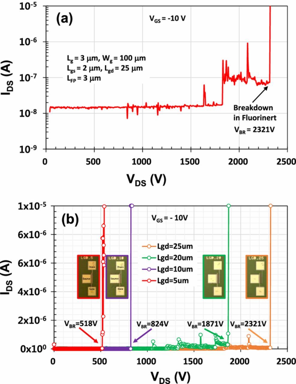
Figure 3. Three-terminal off-state breakdown characteristics of source-connected FP-MOSFETs (a) for Lgd = 25 μm in semi-log scale and (b) for Lgd = 5 μm, 10 μm, 20 μm, and 25 μm in linear-scale at a constant Vgs = −10 V. All breakdown voltages are measured in Fluorinert FC-770 with system compliance of 10 μA, defined as the catastrophic breakdown criteria in this work.
Figure 4 shows VBR and EBR vs. Lgd of the measured devices in this work. The experimental EBR is simply calculated by dividing VBR over Lgd as mentioned reason in previous experimental section. The VBR was monotonically increased with Lgd. The EBR for a device with Lgd = 25 μm was 0.93 MV/cm and other devices also have values near 1 MV/cm, which is similar with reported data by K. Zeng et al.20 However this is very low compared to the expected β-Ga2O3 EBR of 6 − 8 MV/cm,2 3.8 MV/cm for Lgd = 0.6 μm,3 and 5.2 MV/cm for 181 nm-thick β-Ga2O3.4 This means that as the Lgd increases, the breakdown occurs at weaker points such as the dielectric films and FP edge rather than the breakdown of the Ga2O3 itself. In order to utilize the intrinsic EBR of the Ga2O3 channel layer, the dielectric materials used below and above the FP should have large dielectric constant and/or enough thickness.
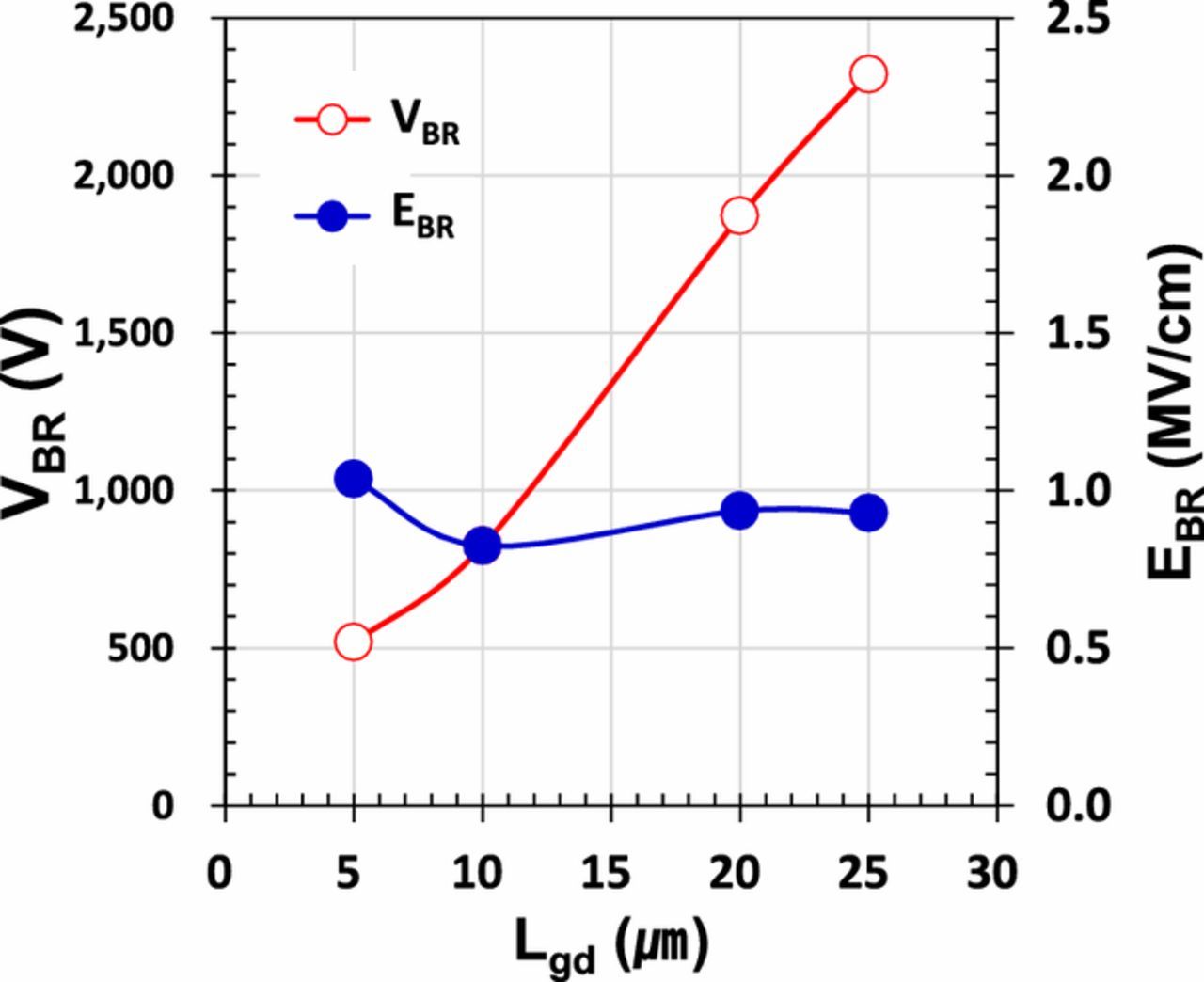
Figure 4. Breakdown voltage VBR and breakdown electric field EBR vs gate-drain spacing Lgd in measured devices. The EBR is simply calculated by dividing VBR (from measurement data shown in Fig. 3.) over Lgd.
Figure 5 shows a comparison of Ron,sp vs. VBR of device figure of merit (FOM) against previously reported lateral Ga2O3 MOSFETs relative to the theoretical limits of Si, GaN and Ga2O3. Developed a source-connected lateral β-Ga2O3 FP-MOSFET with Lgd = 25 μm showed a record high VBR of 2321 V and a Ron,sp of 959 Ω·cm2. This good result is attributed to the optimization of process conditions of plasma enhanced atomic layer deposition (PEALD) of Al2O3 gate dielectric21 and the passivation schemes with internal SiO2 and external Si3N4 dielectric films by PECVD in the device structure as shown in Fig. 1a. Another device with Lgd = 20 μm also showed a high VBR of 1871 V. Previous reported FP β-Ga2O3 MOSFET with same Lgd = 20 μm showed a high VBR of 1850 V and a Ron,sp of about 2100 Ω·cm2.20 Our device shows as high as VBR but very low Ron,sp. This is due to a high doping concentration (1.5 × 1018 cm−3) of the channel. It is noted that high performance power MOSFETs with low Ron,sp and high VBR could be implemented with increasing doping concentration of the thin channel and adopting source-connected FP structure described in this work. In addition to high electrical performances of the Ga2O3-based MOSFETs and SBDs and its excellent material properties, the promising low cost and large-size β-Ga2O3 substrates produced from melt-grown method as well as the high speed epitaxial layer growth techniques can reduce the whole cost of power devices and hence making it possible for commercial products in near future.13,22,23
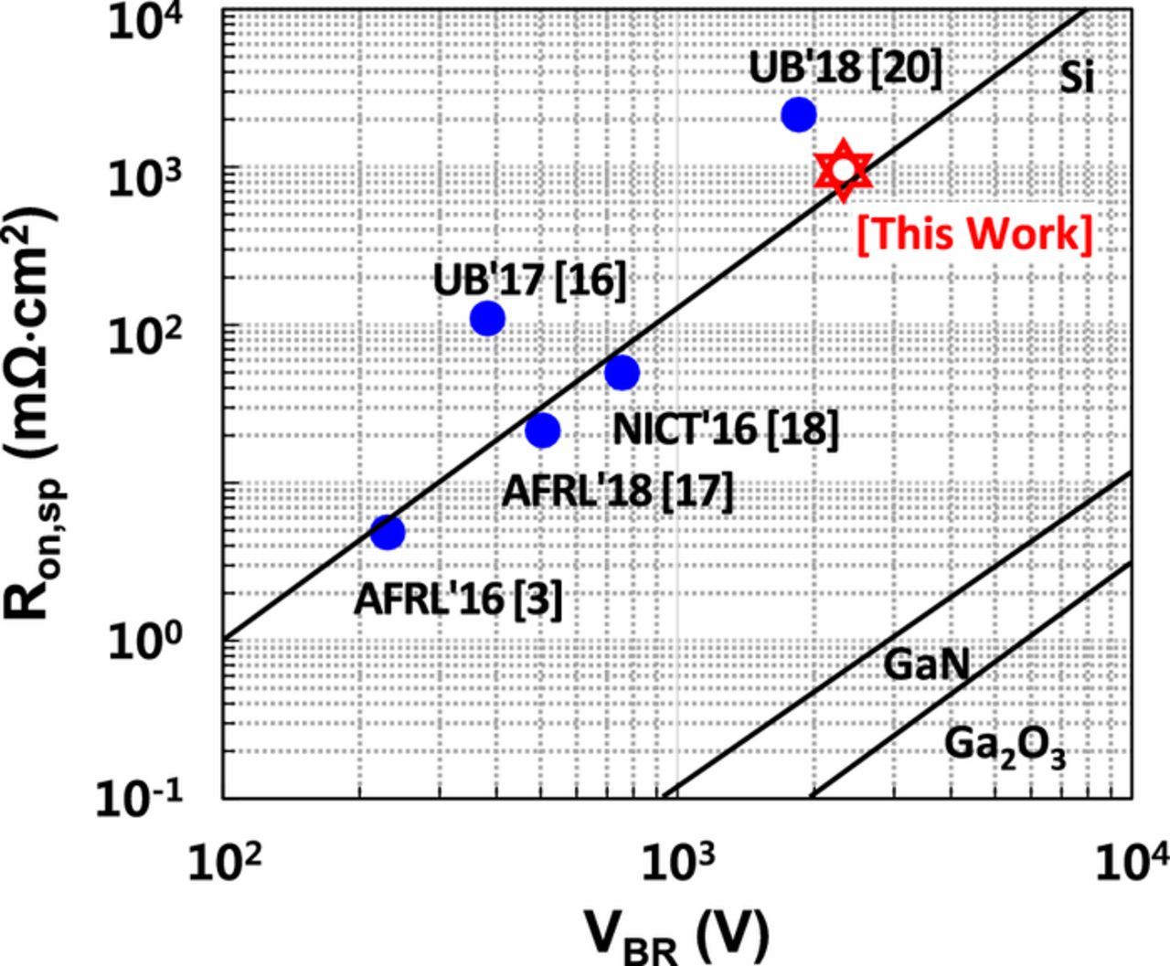
Figure 5. Plot of Ron,sp vs. VBR of device figure of merit (FOM) against previously reported lateral Ga2O3 MOSFETs relative to the theoretical limits of Si, GaN and Ga2O3. Ron,sp in this work is calculated by multiplying the active area to the on-resistance (Rds,on) of the test device (from the reciprocal slope of I-V curve at VGS = + 1.0 V and VDS = 7 V).
Conclusions
High performance lateral β-Ga2O3 MOSFETs with source-connected field plate are demonstrated on Si-doped thin channel layer grown by MBE on Fe-doped semi-insulating β-Ga2O3 bulk substrate. A record-high three-terminal off-state breakdown voltage of more than 2.32 kV is measured in source-connected FP lateral β-Ga2O3 MOSFETs with a gate-drain spacing Lgd = 25 μm and a field plate length LFP = 3 μm. The results indicate that source-connected FP lateral β-Ga2O3 MOSFETs are very promising candidates for next generation high-voltage and high-power switching devices applications above 2 kV. In conclusion, source-connected FP technology provides a stable, low cost and effective way to make high breakdown voltage in lateral β-Ga2O3 MOSFETs.
Acknowledgments
This work was supported by "The Strategic Core Material Development Program (No. 10080736)" of the Ministry of Trade, Industry & Energy (MOTIE), Korea. We thank Dr. In-ho Kang of Korea Electrotechnology Research Institute (KERI) for his support high voltage breakdown measurements.
ORCID
Jae Kyoung Mun 0000-0002-1849-2117
Hyun-Wook Jung 0000-0001-5770-6387