Abstract
Hydrogen (deuterium) absorption into sputter-coated titanium (Ti) film electrodes during cathodic polarization in heavy water (D2O) was monitored using in-situ neutron reflectometry (NR) and electrochemical impedance spectroscopy (EIS). The scattering length density (SLD) of Ti metal increased with increasing cathodic polarization, due to the penetration of deuterium through the surface oxide and into the underlying metal. The rate of D absorption estimated from the NR data showed a pattern with four distinctive regions separated by potential boundaries between −0.35 and −0.4 VSCE and around ∼−0.6 VSCE. EIS results support division of the behavior into these potential ranges. Hydrogen absorption by Ti was observed at potentials <∼−0.35 VSCE, where the capacitance and resistance of the TiO2 layer dramatically changed. At this point, the D content of the film quickly achieved a level of ∼900 ppm by weight (atom ratio D:Ti ∼ 0.04). Decreased absorption kinetics were observed over the potential region from ∼−0.40 VSCE to −0.6 VSCE, indicating that D absorption was controlled either by a diffusion process through the TiO2 layer or by the formation of blocking hydrides at the Ti/TiO2 interface, at the base of the defective locations in the oxide through which the hydrogen was entering. Significant increases in the current density and SLD of the Ti film at potentials more negative than −0.6 VSCE were assigned to widespread hydrogen absorption and TiHx growth within the metal. These observations are consistent with hydrogen ingress through the oxide film, probably via weak points containing electronic defects and disorder, such as grain boundaries and triple points, at potentials as mild as ∼−0.4 VSCE, and with hydrogen penetration through continuous, intact oxide via the previously published redox transformation mechanism, at potentials more negative than −0.6 VSCE.
Export citation and abstract BibTeX RIS
Titanium corrosion processes are often accompanied by hydrogen production. For example, 80% or more of the crevice corrosion process on Ti is driven by the reduction of protons inside the crevice:
![Equation ([1])](https://content.cld.iop.org/journals/1945-7111/160/9/C414/revision1/jes_160_9_C414eqn1.jpg)
This leads to the absorption of atomic hydrogen, and can result in extensive hydride formation.1,2 Cathodic polarization and galvanic coupling with active metals can also cause hydrogen evolution on the Ti surface and hydrogen penetration into the bulk metal. Since hydrogen absorption into Ti structures can lead to their failure by brittle cracking, once the hydrogen concentration achieves a critical level,3 safe operation of such structures requires a detailed knowledge of the mechanism of hydrogen entry into Ti so that exposure conditions that put the structure at risk of hydrogen-induced cracking can be avoided. A number of studies have been done on the physicochemical properties of Ti/H systems, as well as on hydrogen-induced cracking of Ti.3,4 Here we explore the role of the electrochemical potential in determining whether adsorbed hydrogen atoms generated by water reduction can penetrate the native oxide on Ti.
The surface oxide layer plays an important role in protecting the underlying metal from corrosion in an oxidative environment.2,5–7 It also provides a strong barrier to hydrogen entry into the metal phase.5,8–13 The oxide film on Ti is a semiconductor with a wide bandgap of 3.05 eV. Slight deviations from stoichiometry (TiO2−x) give the oxide film n-type characteristics.14 These n-type characteristics can be attributed to a combination of oxygen vacancies and interstitial TiIII ions, which lead to the trapping of electrons in an orbital band just below the conduction band edge.15,16 For hydrogen absorption to proceed, redox transformation (TiIV → TiIII) in the oxide film is necessary (e.g., TiO2 → TiOOH).13 When the oxide is cathodically polarized to potentials below the flatband potential (−0.54 V vs. the saturated calomel reference electrode (SCE)14), redox transformations within the passive oxide lead to the availability of multiple oxidation states of the cation and a consequent increase in the conductivity of the film. This facilitates electron transfer across the film/solution interface and allows the reduction of protons, an electrochemical process accompanied by absorption of H into the oxide.8,11 According to Ohtsuka et al.,13 this coupled redox transformation-hydrogen absorption process can be described by the reaction:
![Equation ([2])](https://content.cld.iop.org/journals/1945-7111/160/9/C414/revision1/jes_160_9_C414eqn2.jpg)
This requires significant cathodic polarization of the metal, generally only achievable by galvanic coupling to active materials, such as carbon steel, or the external application of a sufficiently negative potential.
Hydrogen permeability, as reported by Murai et al.,8 is only significant at potentials <−0.7 VSCE. An average threshold potential of −0.6 VSCE, positive of which no hydrogen absorption and hydride formation occurs, has been suggested,1,9 and several studies5,11 have claimed that hydrogen is not transported through the oxide film at any significant rate until a potential of ≤−1.0 VSCE is reached. In apparent contradiction of these previous works, Zeng et al.,12 using a Devanathan cell to monitor hydrogen transport across sputter deposited TiO2, detected hydrogen penetration through the oxide at potentials >−0.6 VSCE, and determined a threshold potential of only −0.37 VSCE for hydrogen ingress.
Recent studies by Zhu et al.17,18 on the properties of cathodically polarized Ti oxides showed that the hydrogen barrier properties of the oxide are strongly dependent on oxide composition and structure. These experiments demonstrated that grain boundaries and the locations of intermetallic particles in the Ti (from either alloying elements or impurities) tend to be more cathodically reactive than the α-titanium grains themselves, displaying local cathodic current and oxide reduction at more positive potentials than the surrounding regions of the surface. Given these complexities, it is difficult to predict the potential at which hydrogen will be transported through the oxide and what fraction of the hydrogen atoms generated on the oxide surface will actually reach the metal.
Neutron reflectometry (NR), amongst other techniques for detecting hydrogen, is the most powerful and perhaps the best method for studying hydrogen ingress into metals.19–30 This ability is empowered by the high contrast between hydrogen isotopes (hydrogen and deuterium) which can be used to precisely probe, non-destructively, the amount of hydrogen penetrating into the metal and any surface films. The fact that NR can be carried out in situ by applying a controlled electrochemical condition adds a new dimension to the study of hydrogen transport through the oxide and metal films, and of their corrosion resistance. We herein report a NR experiment in conjunction with electrochemical impedance spectroscopy (EIS) to address the aforementioned issues. In particular, we investigated potential-driven hydrogen absorption in titanium metal under a wide range of cathodic polarizations.
Sample and Equipment
The sample was a ∼50 nm thick Ti film, sputter-deposited on a Si(111) substrate in an Ar atmosphere. A sputtering target-grade Ti disk (American Elements, PN:TI-M-03-ST.2250, 99.9% Ti), pre-cleaned with Argon plasma, was the source of the metal. Upon removal of the substrate from the sputtering chamber and exposure to air, the native oxide grew on the Ti film. This sample preparation predated the NR experiment by ∼1 month; the oxide layer is expected to have grown to ∼4 nm in thickness by the time that we began the NR experiment.31 The cell, designed for performing NR and electrochemical measurements simultaneously on the same sample, has been fully described by Noël et al.11 When the cell was fully assembled and filled with electrolyte, the Ti thin-film became the working electrode. All aspects of the electrochemical measurements were performed via a potentiostat (Solartron 1287) and a frequency response analyzer (Solartron 1255B) controlled by a computer running CorrWare and ZPlot software (Scribner Associates).
NR was performed on the D3 reflectometer at the NRU Reactor, Chalk River, operating with a fixed neutron wavelength of 0.237 nm. Equipped with motorized high-precision slits, the reflectometer performed 2θ/θ scans while maintaining a constant beam footprint on the sample and a fixed step size of 0.01 nm−1 in the momentum transfer vector (Qz). The incident neutron flux on the sample, Bi, was measured by positioning the detector at 2θ = 0° while varying the slits exactly as in a scan. The Qz-dependent background was measured by offsetting the sample by 0.3° vs. the incident angle. Dividing the background-subtracted reflected intensity by Bi yielded the reflectivity on the absolute scale. The normalized data thus obtained were analyzed by least-squares fitting a layer profile model using the Parratt32 program.33
Measurement Procedure
Before initiating the electrochemistry part of the experiment, we performed NR scans on the as-prepared sample, with three different sample configurations. These were mainly done to verify that the reflectometer was functioning properly, but they also served to characterize and align the sample on the instrument. The configurations were as follows:
- (a)Sample clamped to a bracket with the incident (and the reflected) beam on the air-side of the thin-film.
- (b)Sample clamped to the same bracket but with the incident beam on the Si-side (substrate side) of the thin-film.
- (c)Sample mounted on the empty electrochemical cell (i.e., no electrolyte solution, but the cell was otherwise complete) with the incident beam on the Si-side. This geometry is necessary when the sample is mounted on the cell, since neutron access from the air-side is blocked by the cell body.
After the measurements taken with the sample in configuration (c), the cell was filled with a solution of 0.27 M NaCl (neutral pH, argon-deaerated) in heavy water (D2O). The area of the working electrode exposed to the solution was 62.5 cm2. For the entire experiment, the working electrode potential was measured vs. a saturated calomel electrode (SCE). In this paper we exclusively applied potentiostatic polarization, with cathodic currents conventionally expressed as negative numbers.
As soon as the cell was filled with electrolyte solution, we began monitoring the open circuit potential (EOC) of the working electrode. Subsequently, we applied a potentiostatic polarization and recorded the current through the working electrode during the first two hours, while we waited for the current to achieve a steady state. After that, we maintained the same potentiostatic bias and recorded the impedance spectra.
For electrochemical impedance spectroscopy (EIS) a sinusoidal input potential of 20 mV amplitude, scanned over a frequency range from 100 kHz to 1 mHz, was applied, in addition to a dc bias, while we recorded the complex impedance Z(ω) = Z'(ω) + jZ''(ω), at each angular frequency, ω, where j2 = −1, and Z' and Z'' are the real and imaginary components of the impedance, respectively. The first set of EIS scans was performed with the potential, E, set to 0 VSCE. The scans, each lasting 1.2 h, were repeated five times to see whether there was any trend in the run-to-run variations in the impedance data. If there was no systematic variation detected, all data collected at a single applied potential were combined (via point-by-point averaging of Z' and Z'' acquired at each frequency) for analysis and plotting.
The first set of NR scans in the presence of electrolyte solution was performed while the EIS scans at E = 0 VSCE were in progress. A total of eight identical NR scans were carried out. The purpose of repeating these NR scans, each performed within ∼1.2 h (i.e., relatively quickly), was again to see if there was a trend in the run-to-run variations in the NR data.
During the remainder of the experiment we probed the sample with EIS and NR as it underwent changes in response to increasingly cathodic polarization. Measurements were performed with E held at −0.25, −0.30, −0.40, −0.45, −0.50, −0.55, −0.60, −0.65, and −0.70 VSCE, in that sequence. The procedure during each polarization was as follows: we monitored the cell current beginning almost immediately after we set E, and started the NR scan (from high to low Qz) within a few minutes thereafter. The NR scan was repeated twice, taking a total of 10 h. Simultaneously, the cell current was monitored for the first 2 h and then EIS scans performed repeatedly for the remaining ∼8 h.
Because these experiments demand extensive allocation of precious neutron beam time, all of the measurements reported herein were performed once, on a single Ti thin film sample. We intend to repeat this work on another nominally identical film, using H2O solution in place of D2O as both a confirmation of full reproducibility and as a complement to the current measurements, due to the differences in the interactions of the neutrons with H and D.
Results
The reflectivity data obtained with all three sample configurations are of good quality, for instance, normalized reflectivity from configuration (a), shown in Figure 1 (circles), covers more than 6 orders of magnitude with little background at the high-Qz end. The quality and dynamic range of the data obtained with configurations (b) and (c) are similar to those obtained in configuration (a).
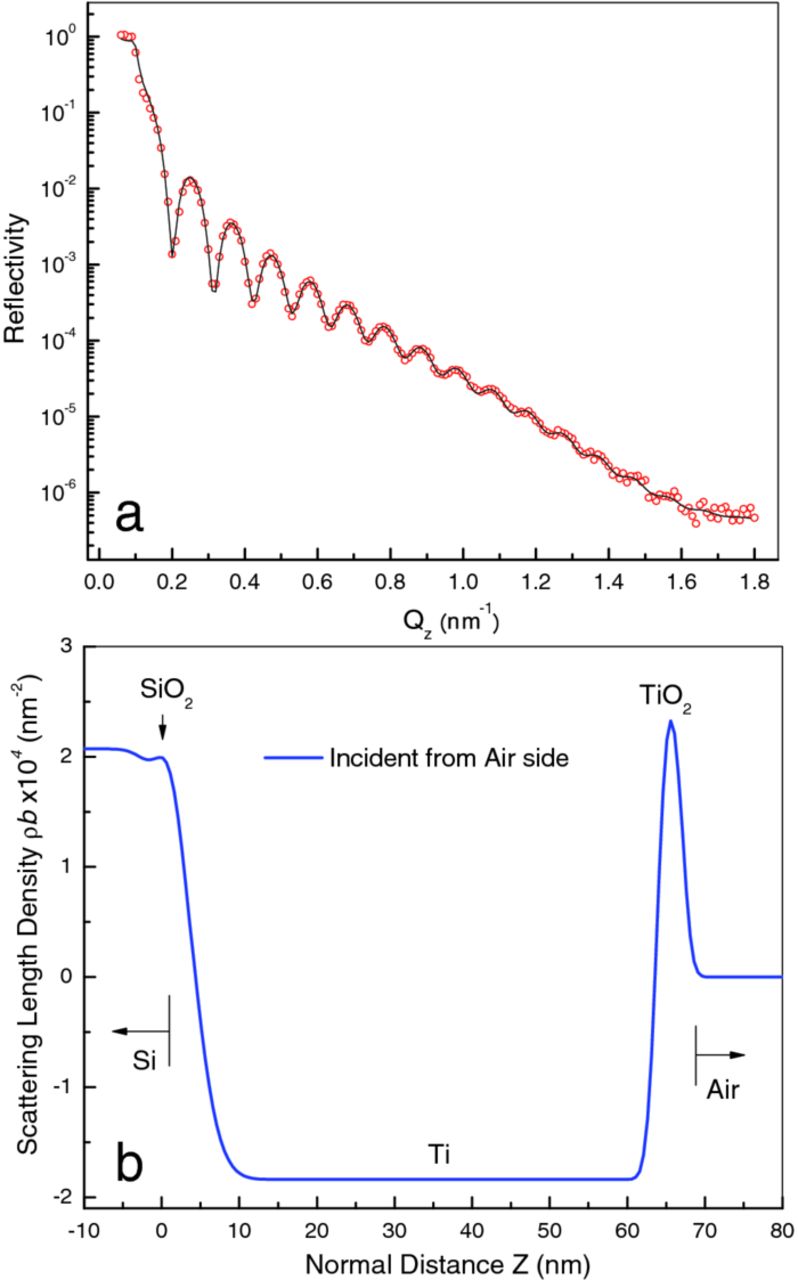
Figure 1. (a) Experimental NR data points (open circles) measured for a Ti thin film sputter coated on a Si wafer. This is for the stand-alone sample, with neutrons impinging from the air side. The fitted curve (black) corresponds to the model with the fitting parameters shown in Table I. (b) The real space layer profile of the model that best fit the data of panel (a), showing the SLD and layer structure of the sample surface.
Table I. Model parameters used to fit the data and obtain the real space profile shown in Figure 1.
| – | d (Å) | Re{ρb} (Å−2) | Im{ρb} (Å−2) | σ (Å) |
|---|---|---|---|---|
| Air | N/A | 0 | 0 | |
| TiO2 | 33.16 | 2.635 × 10⁻⁶ | 0 | 9.298 |
| Ti | 605.37 | −1.838 × 10⁻⁶ | 0 | 10.207 |
| SiO2 | 31.83 | 3.35 × 10⁻⁶ | 4.056 × 10⁻⁷ | 29.366 |
| Si | N/A | 2.073 × 10⁻⁶ | 2.376 × 10⁻¹¹ | 14.37 |
Open-circuit potential (EOC) monitoring began immediately after we filled the cell. The EOC initially read by the potentiostat was 0.035 VSCE, but drifted to 0.005 VSCE over the course of a few hours. Routinely observed, drifts in EOC are usually due to slow changes, either in the electrolyte or on the surface of the working electrode. After allowing the working electrode to be exposed to the solution for several hours at open circuit, we polarized it at a series of potentiostatic values while completing the rest of the experiment. Although the initial potential applied (0 VSCE) was slightly <EOC at the time it was applied (0.005 VSCE), ongoing minor changes resulted in small anodic currents being observed until the potentiostatically applied polarization was stepped to a sufficiently negative value that the current became cathodic.
The results of EIS scans, performed once the working electrode achieved a steady state, agreed with each other within experimental error, indicating that changes to the sample, if any, were too small or slow to be observed on the time scale of hours. An example of the combined EIS data collected at E = 0 VSCE is shown in Figure 2, along with the fitted impedance curve, to demonstrate the quality of the fit to the data. The equivalent circuit model that was used to fit the data is included as an inset within Figure 2.
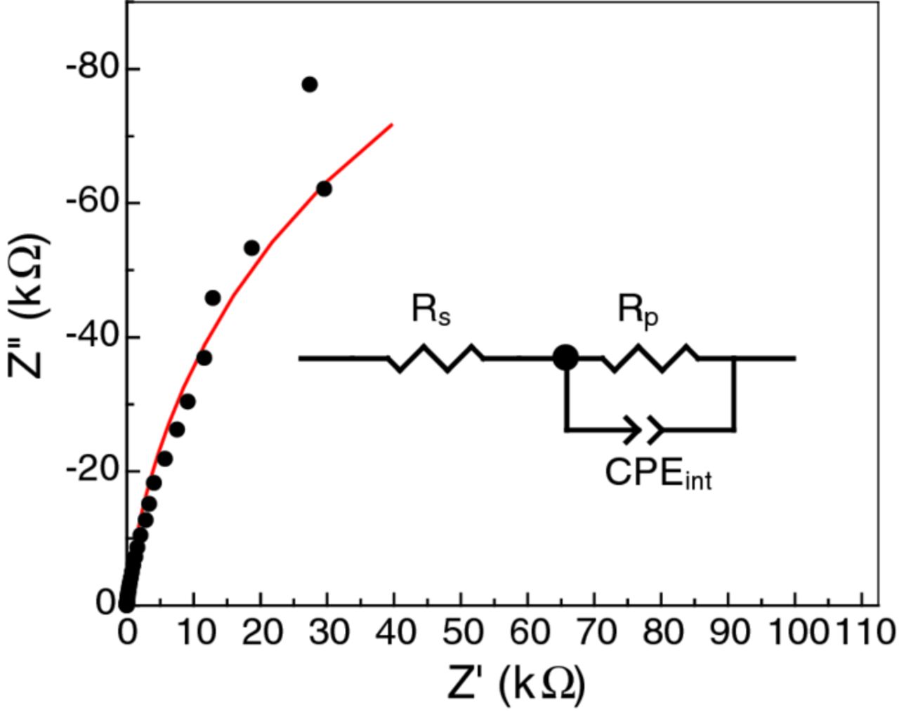
Figure 2. The average of five EIS measurements (black dots) at each frequency recorded in 0.27 M NaCl in D2O solution at E = 0 VSCE on the Ti thin film electrode that was sputter coated onto a Si wafer. The least-squares fitted curve (red) was obtained using the equivalent circuit model shown inset.
Since no systematic variation was found in the repeated NR scans under the same conditions, all NR data were combined and averaged, leading to the plot shown in Figure 3. Due to the superfluous neutron scattering from D2O, the background in the high-Qz region was significant and the dynamic range of the data reduced (compare to Figure 1).
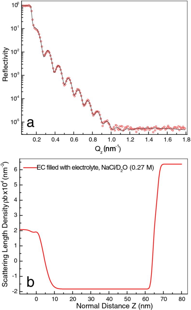
Figure 3. (a) The average of eight NR measurements (open circles) in 0.27 M NaCl/D2O solution for the Ti thin film sputter coated on a Si wafer. The fitted curve (black) corresponds to the model with the parameters shown in Table II. (b) The real space layer profile of the model that best fit the data of panel (a), showing the SLD and layer structure of the sample surface.
Table II. Model parameters used to fit the data and obtain the real space profile shown in Figure 3.
| – | d (Å) | Re{ρb} (Å−2) | Im{ρb} (Å−2) | σ (Å) |
|---|---|---|---|---|
| Si | N/A | 2.073 × 10⁻⁶ | 5.71 × 10⁻¹¹ | |
| SiO2 | 34.76 | 3.324 × 10⁻⁶ | 0 | 16.327 |
| Ti | 607.03 | −1.831 × 10⁻⁶ | 0 | 33.171 |
| TiO2 | 26.08 | 2.79 × 10⁻⁶ | 5.876 × 10⁻⁷ | 5.776 |
| D2O | N/A | 6.366 × 10⁻⁶ | 9.25 × 10⁻¹⁴ | 8.103 |
As shown in Figure 4 by the constancy of the current at each applied potential, the 2 h wait was long enough to stabilize the changes in the sample in all cases except at −0.65 VSCE and probably −0.60 VSCE. The observation that the impedance measured by all repeated EIS scans is constant within experimental error is further evidence of stability. Also, the reflectivities observed by the two NR scans at each potential are similar (within errors) suggesting that most of the changes to the sample took place during the time it took to record the background region (Qz > 0.1 Å−1 in Figure 3) of the first scan.
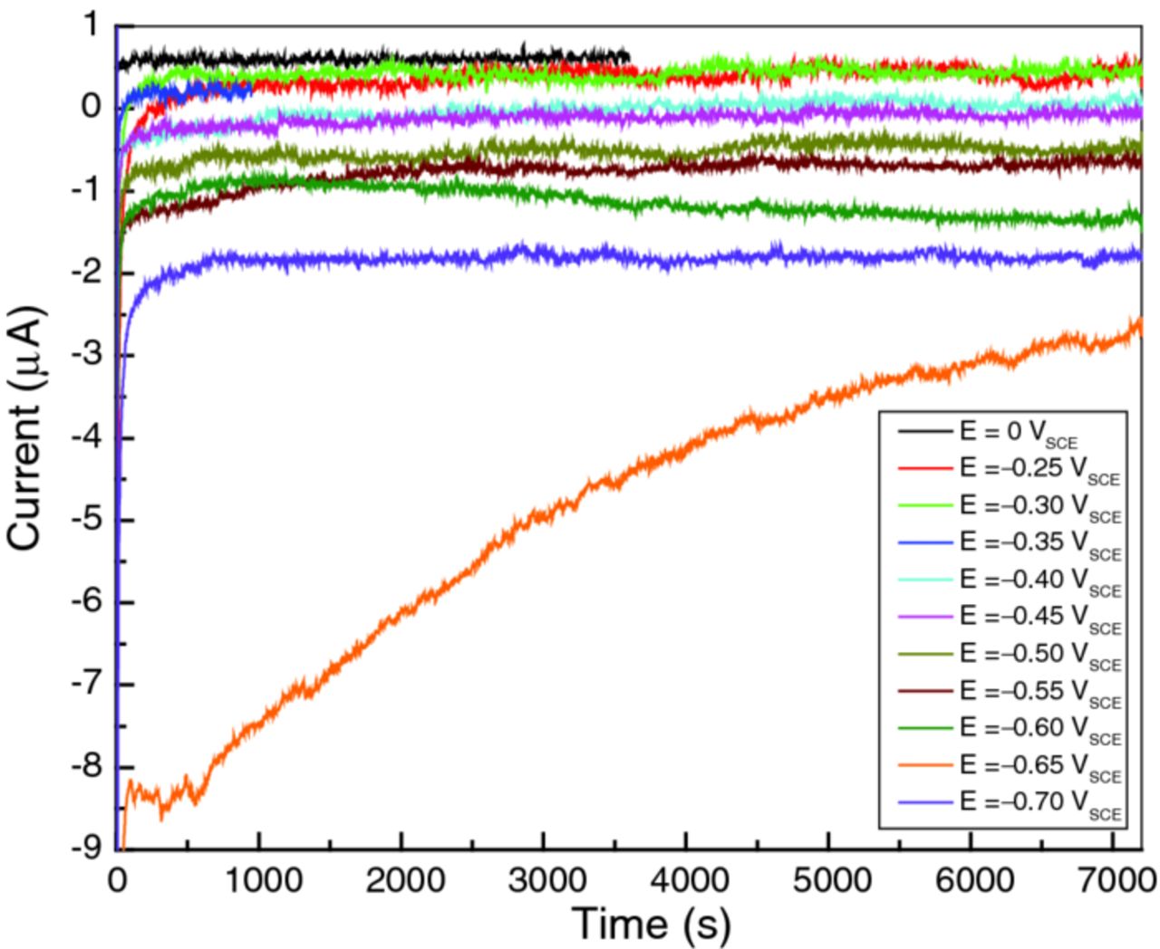
Figure 4. Current transients measured at different potentials, as indicated. The maximum current was seen at E = −0.65 VSCE.
Figure 4 shows current transients recorded within the first 2 h after we set the polarization E. As expected, decreasing the potential caused the cathodic current to increase momentarily, spiking to a more negative value, and then settling over time (typically within 10 minutes) to a new steady state. Remarkable deviation from the general trend occurred at −0.65 VSCE. Not only was the transient cathodic current much higher, but it also took a long time to stabilize: indeed, the cathodic current was still decreasing after 2 h. Closer inspection of the current transient data revealed that this behavioral change started at −0.60 VSCE. Approximately 1 h after we set E at −0.60 VSCE, the cell current started to rise (i.e., became more cathodic in Figure 4), and thereafter showed fluctuations larger than seen at all previous potentials. The consequences of this change are visible in the EIS results (Figure 5). The data at E = −0.55 VSCE (panel a) show a spread that is relatively small and random in sequence, whereas those at −0.60 VSCE (panel b) arc significantly more and exhibit a systematic trend. In fact, the trend to higher impedance over time at −0.60 VSCE indicates a reversal in the initial trend to higher cathodic currents observed during the first 2 h of the experiment (Figure 4). This change was nearly complete by the time EIS was performed at −0.65 VSCE (not shown), all the Nyquist plots (except the first) arcing less than those at −0.60 VSCE with a small and random distribution. Figure 6 is a summary of all the EIS results.
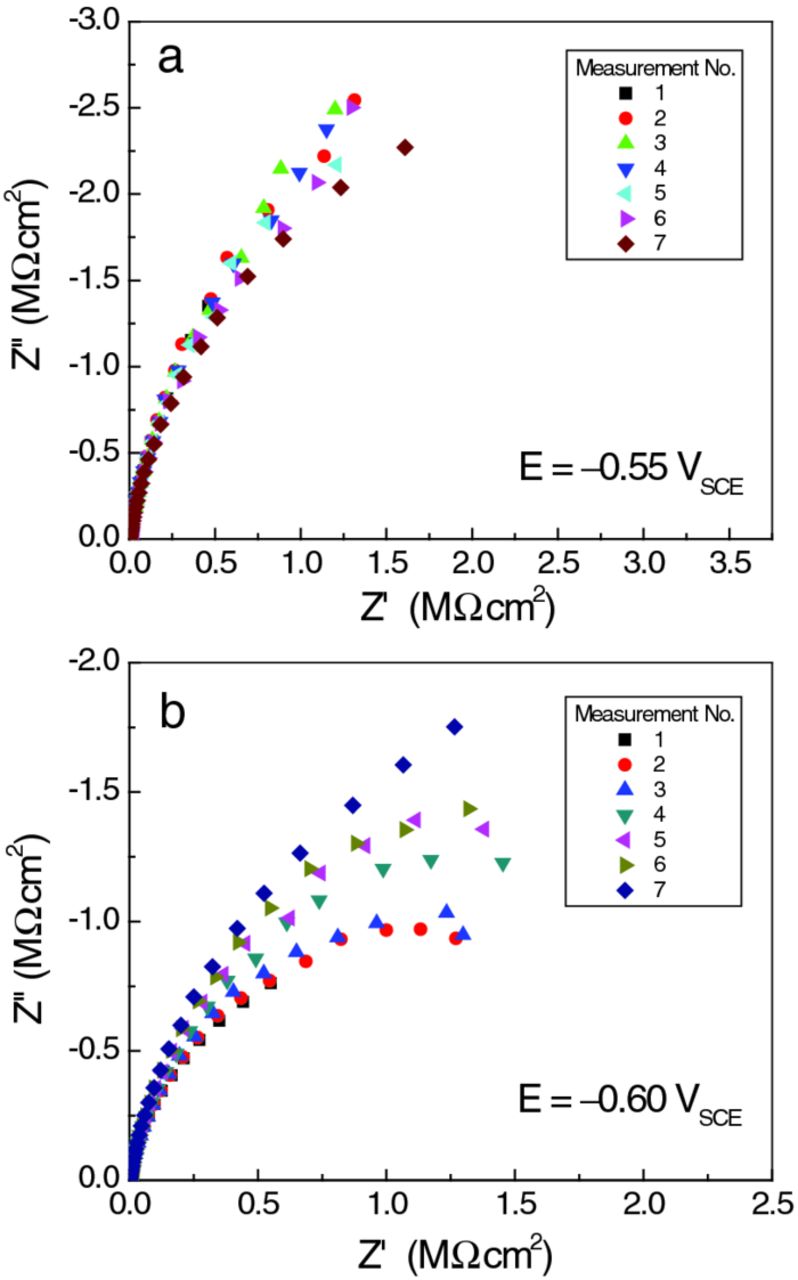
Figure 5. Nyquist plots for sets of consecutive EIS measurements during the NR scans at (a) E = −0.55 VSCE, and (b) E = −0.60 VSCE, showing that the electrode impedance at E = −0.60 VSCE changed much more than did that at −0.55 VSCE during the ∼12 hour duration of the NR scan.
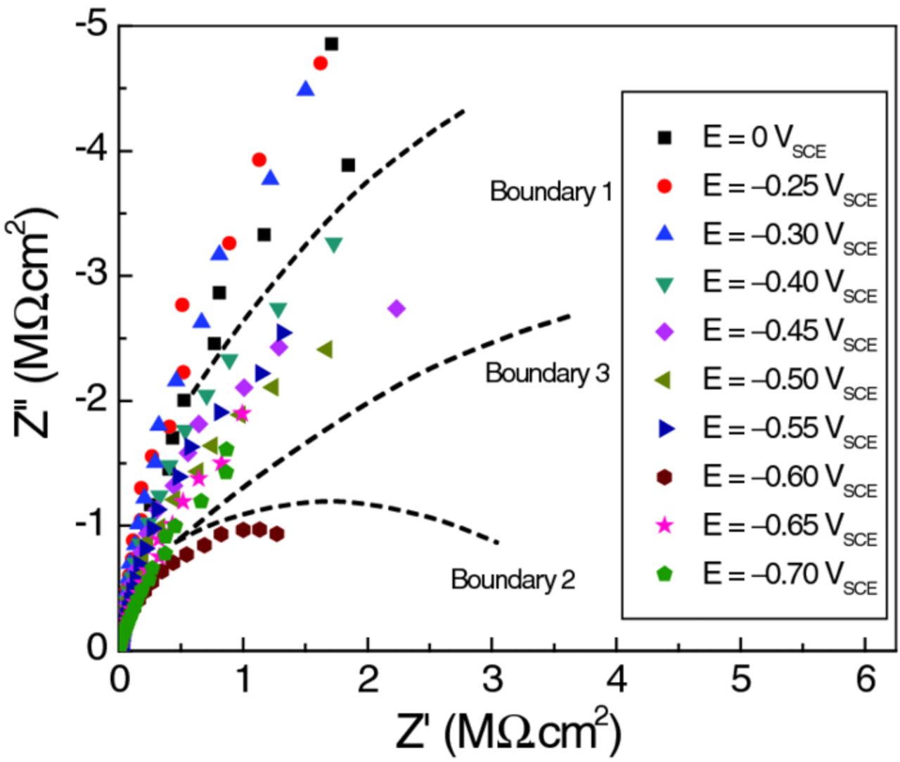
Figure 6. Nyquist plots of EIS data measured at ten different potentials, as indicated, overlaid for comparison. The data fall into four different groups separated by three different potential boundaries. The most significant changes were observed between potentials of E = −0.3 VSCE and −0.4 VSCE and at E = −0.60 VSCE.
Physical model for the NR data
Careful analysis of the NR data on the as-prepared sample (Figure 1) in terms of a model serves two purposes: 1) it characterizes the sample in its original state, and 2) it gives a measure of the uncertainty in the parameters obtained using the least-squares fitting procedure.
Ideally, a single model should fit all three sets of data acquired on the as-prepared sample in the three configurations employed. The model we chose after proposing and investigating numerous possibilities consists of five distinct media representing air, TiO2, Ti metal, SiO2 and Si substrate. Each medium is represented by a plateau, a region of constant scattering-length density (SLD or ρb, where ρ is the number density of the nuclei present and b their coherent neutron scattering length, a characteristic property of each element and isotope). The thickness, d, is infinite for the first and the last media but finite for the central media (e.g., d(Ti) for the Ti layer). The interface between two media is represented by a hyperbolic tangent function of width parameter σ. Our model is consistent with the axiom of "simplest possible," as no feature was included unless it led to a significantly better fit to the measured reflectivity.
The Parratt32 program33 used for model refinement can fit only to a single data set at a time (with no option for coupled refinement). Consequently, independent refinements were performed on the reflectivity data for the three different configurations of the as-prepared sample, and the refined parameters compared. The parameters and values for the as-prepared sample in configuration (a) are listed in Table I. The table shows the best fit values for the layer thicknesses (d), the real and imaginary components of the scattering length density (Re{ρb} and Im{ρb}, respectively), and the interfacial roughness parameter, (σ). The calculated reflectivity corresponding to the model is shown in Figure 1a, and the layer profile of the model is given in Figure 1b. The agreement between observed and calculated reflectivity is excellent in all cases.
Figure 7 is a plot of the models representing the as-prepared sample in the three measurement configurations on a common scale (the profiles for sample configurations (b) and (c) were reversed and the origins shifted to match that of configuration (a)). The agreement is good, except at the TiO2/air interface, which is much broader in configuration (c). In all cases, Ti is the only layer thick enough to exhibit a plateau in SLD, whereas the SiO2 and TiO2 layers are so thin that the interfaces on either side of the layer merge and no plateau is visible. The lower peak for TiO2 in configuration (c) is a consequence of the merging of the two closely spaced interfaces. The magnitude of ρb observed for Ti is significantly smaller (i.e., a less negative number) than that of bulk Ti (−1.95 × 10⁻⁴ nm−2). This is common for sputter-deposited films, and is most probably due to the formation of vacancies or incorporation of impurities, such as oxygen, during sputtering.32 The peak ρb values for the SiO2 and TiO2 layers (discounting the empty cell case, configuration (c), for the latter) are surprisingly close to the bulk phase values, 3.62 × 10⁻⁴ nm−2 and 2.63 × 10⁻⁴ nm−2, respectively, considering that these layers are too thin even to show a SLD plateau.
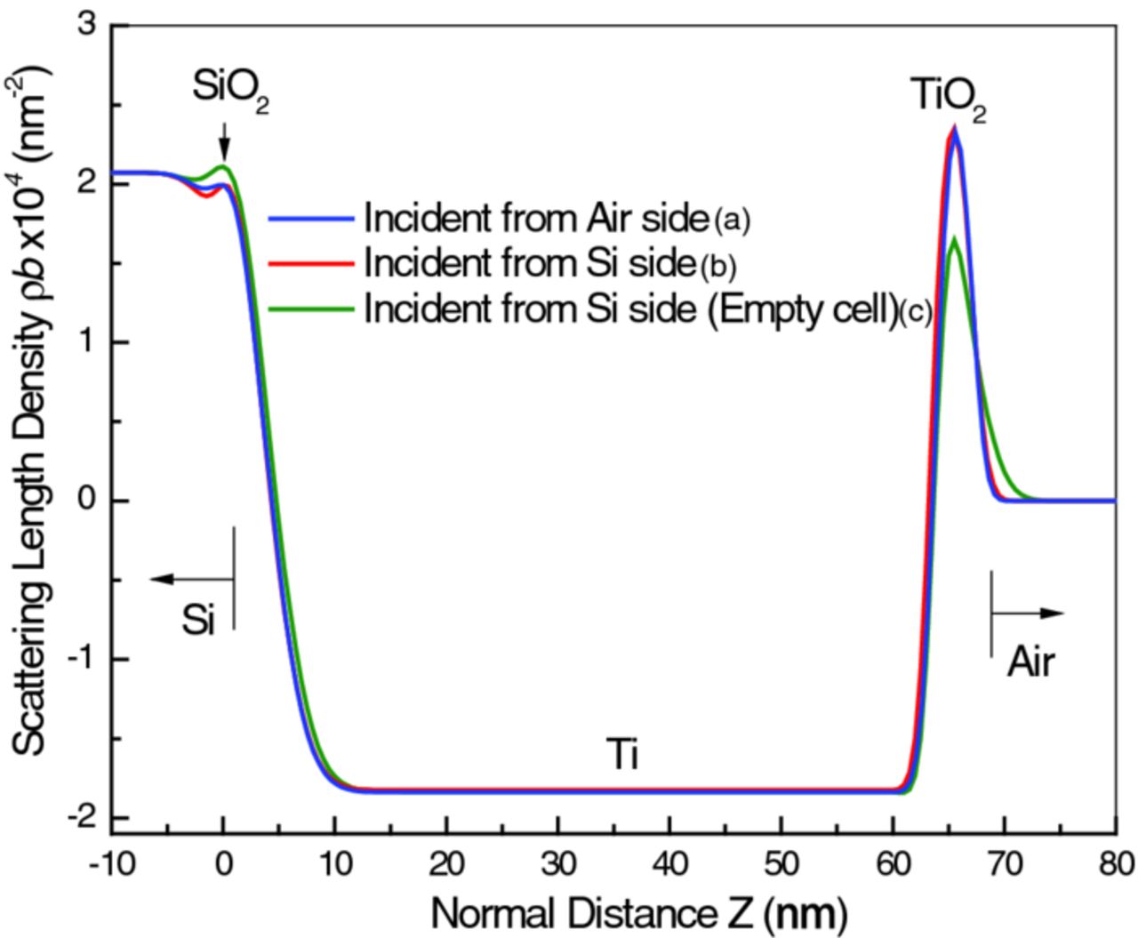
Figure 7. SLD profiles for the least-squares fitted models proposed for the same as-prepared sample in air, in three different configurations, as indicated, plotted together for comparison. The blue curve corresponds to the stand-alone sample measured in air with neutrons incident from the air side. The red curve is the profile for the stand-alone sample measured in air, but with neutrons incident on the film through the Si substrate, and the green curve corresponds to the sample mounted on the empty electrochemical cell (EEC). The latter two profiles have been reversed and the origin shifted for better comparison with the profile generated from the first configuration. As explained in the text, the difference between the profiles of the stand-alone and EEC-mounted sample could be due to either a slight deformation of the sample under the extra pressure applied by clamping or, more probably, the extra neutron background contributed by the electrochemical cell body components around the sample.
The change seen for the TiO2/air interface in configuration (c), while suggestive of either mechanical deformation of the sample during mounting on the cell or a compositional change, is actually an artifact. Sample deformation would affect all of the layers within the sample, not just the outermost, which was not the case, and compositional change is unlikely since the sample was not exposed to any different chemical environment. Instead, the change of the interface width and the TiO2 SLD is an erroneous result, probably due to incomplete handling of the increased background signal (not shown) that was observed in this configuration. However, this deficiency became almost irrelevant when the cell was filled with D2O solution, Figure 8, as discussed below.
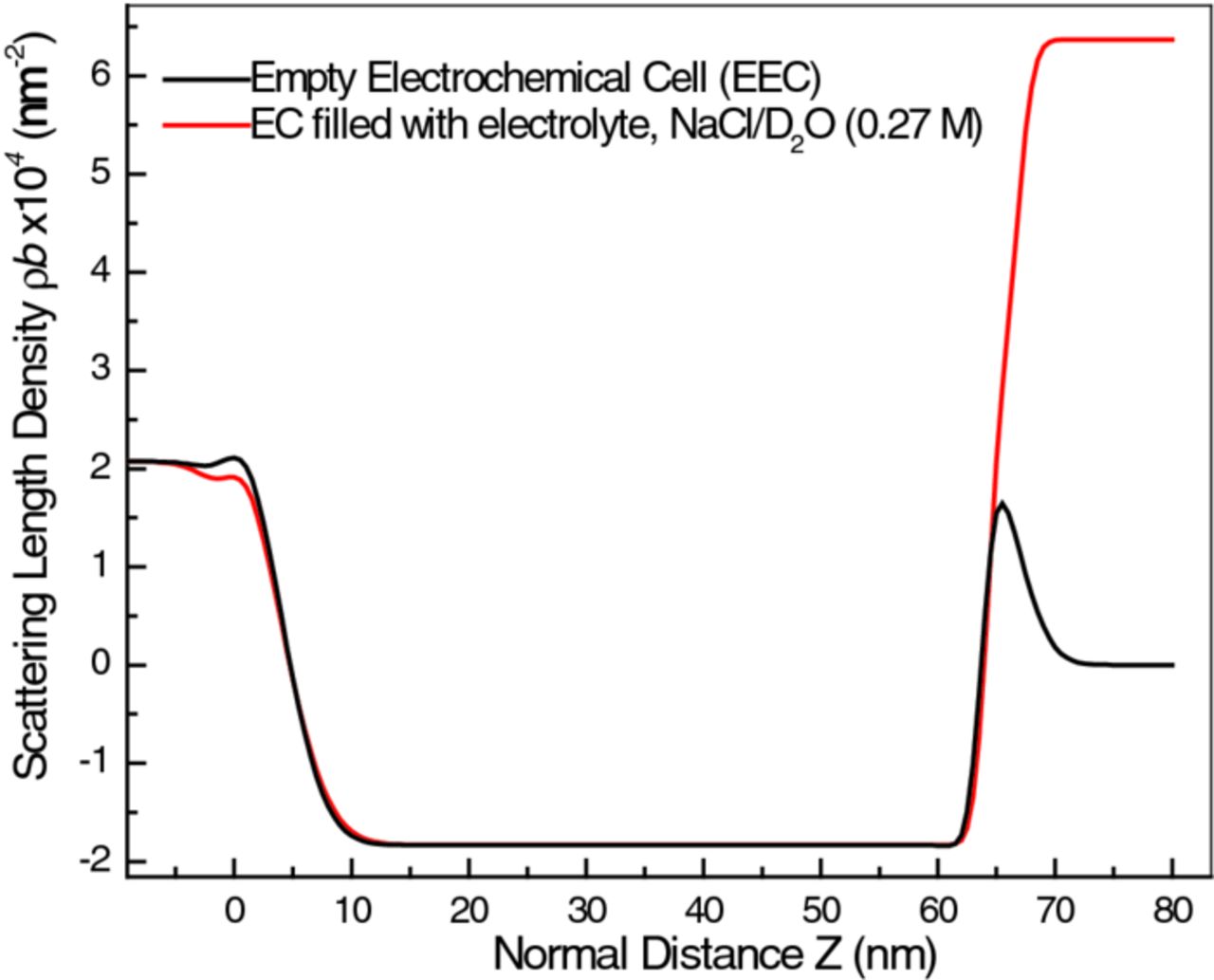
Figure 8. Overlay of the SLD profiles for the Ti thin film sample in the presence and absence of electrolyte solution. The significant contrast between the SLD of the electrolyte (NaCl in D2O) and Ti metal hides the contribution of the native TiO2 layer.
The same model, but with the air (SLD = 0) replaced with D2O (SLD = 6.37 × 10⁻⁴ nm−2) gives excellent fit to all the reflectivity measured subsequent to filling the cell. As noted above (Figure 3) the increase of background caused by D2O is very large. Nevertheless, thickness and SLD values of all the layers refined to sensible values (see Table II). In Figure 8, the black curve is the model used to fit the reflectivity data collected in configuration (c), while the red curve is the model obtained after filling the cell (at E = 0 VSCE). The rise in SLD from Ti (negative) to D2O (highly positive) is so large that one broad hyperbolic tangent function appears to mask the whole Ti/TiO2/D2O interface region (from position ∼60 to 70 nm). As the reflectometry model is not critically sensitive to the TiO2/D2O interface width, the sample's outer surface did not influence any of the subsequent analyzes. For the same reason, we lost the ability to follow with NR the changes occurring in the TiO2 layer as the cathodic polarization was applied.
Since we recorded multiple NR data sets on the same as-prepared sample (Figure 7), differences between least-squares fitted thickness, SLD, and interface width values allow estimation of the uncertainties associated with our analysis. Since parameters associated with well-resolved features should be more reliable, those associated with the Ti layer should show a higher degree of consistency. All the Ti layer thickness values, d(Ti), determined for the as-prepared sample agree to within ±0.2 nm, while the spread in SLD, ρb(Ti), is only ±2 × 10⁻⁶ nm−2. Similar consistencies are seen for the SiO2 layer, both in the thickness and in the SLD, but the spread in d(TiO2) is significantly larger, suggesting an uncertainty of ±0.4 nm. Values of the interfacial width parameter, σ, differ significantly, which is not surprising since σ values are generally more difficult to determine accurately. This prevents us from drawing conclusions that depend critically on interfacial widths.
The errors above are the upper limit for uncertainties, since the sample was physically removed and remounted in a different geometry between the three measurements. However, during in-situ NR and EIS measurements the sample was not physically disturbed. Consequently the precision (but not necessarily the accuracy) of results from successive NR scans should be significantly higher.
The data from two NR scans at −0.25 VSCE, and others at more negative potentials, were analyzed using the same 5-layer model. The fitted results from the two scans agreed very well, suggesting that steady-state was achieved promptly after we set the potential. The parameters presented here are exclusively from the second of the two NR scans.
EIS analysis
In the fitting and analysis of EIS results, the cell can be represented by a single time-constant equivalent circuit consisting of a parallel combination of a constant phase element, CPEint, and a leakage resistor, Rp, in series with the solution resistance, Rs. This circuit is shown inset in the Nyquist plot in Figure 2. All EIS data were analyzed by least-squares refinement of this circuit using ZView software (Scribner Associates). The good fit of model to data is evident in Figure 2.
Discussion
A unique feature of neutron reflectometry is that the experimentalist can sometimes control, at least in part, the sensitivity or contrast between different phases within a sample by changing their SLD, denoted ρb, where ρ is the number density (atoms per unit volume) and b the coherent neutron scattering-length of the isotope. For systems consisting of solids and liquids we usually have no means of affecting the density, ρ, but we can sometimes change the scattering length, b, by choosing the isotopes of the elements involved. The coherent neutron scattering lengths, b, for Ti and H are negative (respectively−0.344 fm and −0.374 fm), while that for D is positive, with a magnitude (+0.667 fm) approximately twice that of b(H). Since the SLD of a phase containing more than one type of nucleus is the weighted average of the ρb values for each type of nucleus present, a small amount of H, dissolved into Ti without causing the metal to swell significantly, will shift the overall ρb of the metal layer in the negative direction. On the other hand, D in Ti will cause the overall ρb to shift in the positive direction and the magnitude of the shift will be twice as large as that observed for an equal amount of H. This is why we used D2O instead of H2O as the electrolyte. However, this advantage comes at a cost; as seen in Figure 8, filling the cell made the SLD profile of the TiO2 layer and the adjacent interfaces all blend into a single step. This made the parameters for the TiO2 layer that were measured by NR after the cell was filled with heavy water untrustworthy, even though they may seem reasonable. This is not the case when the cell is filled with H2O.32
In contrast to NR, EIS results are isotope-independent, since even at the highest frequency measured, 100 kHz, molecular vibrational or rotational responses are undetectable. Given that the Ti layer is metallic, the resistance and capacitance probed by EIS are exclusively from the TiO2 layer, the oxide/solution interface, and the electrolyte solution; i.e., the regions NR cannot "see". Thus, NR and EIS play complementary roles in our experiment.
The EIS data presented in Figure 6 give the overall picture of the stages the sample went through as the potential was decreased. The data fall into four groups as demarcated by the dashed boundary lines in the figure:
- Group 1: Data collected at E = 0, −0.25, and −0.30 VSCE: These data lie above Boundary 1. No EIS measurement was made at −0.35 VSCE, but the cell current (Figure 4) suggests that −0.35 VSCE belongs to this group.
- Group 2: Data collected at E = −0.40, −0.45, −0.50, −0.55 VSCE: These data lie below Boundary 1 but not far from it.
- Group 3: Not really a group since it consists of only one data set, E = −0.60 VSCE, but treated on its own since it is unique. Having a uniquely small low-frequency impedance, these data lie below Boundary 2.
- Group 4: Data collected at E = −0.65 VSCE and −0.70 VSCE: The impedance measured at low frequencies increased over that seen at E = −0.60 VSCE, but remained lower than the low-frequency impedance at less cathodic polarizations. All of these data lie above Boundary 3 but not very far from it. The cell current was high during the first 2 h at E = −0.65 VSCE (Figure 4), but by the time of the last EIS scan the current had settled down to a lower value (as signaled by the increased impedance at the low-frequency end of the EIS scan).
The results in Figure 6, analyzed in terms of the one time-constant equivalent circuit, lead to Figure 9. As Figure 9 was derived from the data in Figure 6, it is not surprising that it shows the same groupings; however, because it emphasizes different aspects of the data than do the Nyquist plots of Figure 6, Figure 9 makes the behavioral differences that led to the group assignments much more clear. Further support for the assignments of Groups 3 and 4 is evident in the different time trends in the currents, visible in Figure 4.
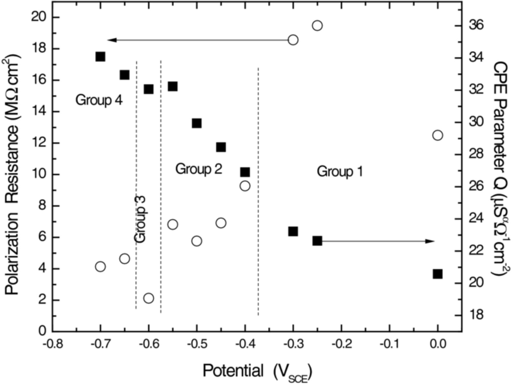
Figure 9. Variation in the resistance and capacitive behavior (as represented by the constant phase element parameter, Q) of the Ti thin film electrode as a function of applied potential, measured in 0.27 M NaCl/D2O solution. Values were extracted from the least-squares fitted electrical equivalent circuit model shown in Figure 2. All of the data have been area normalized.
At small cathodic polarizations (up to about −0.35 VSCE) the cell was characterized by high resistance and low capacitance, as represented by the CPE parameter, Q (Figure 9). A notable decrease of resistance and increase of Q took place between −0.3 VSCE and −0.4 VSCE. At −0.6 VSCE, the resistance fell to a sharp minimum, while Q experienced an inflection in the trend to that point. At E = −0.65 VSCE, the resistance increased a little and Q resumed an increasing trend. We can identify two potentials where significant changes took place, the first critical potential somewhere between −0.35 and −0.40 VSCE, and another at approximately −0.60 VSCE.
The use of a constant phase element rather than a capacitor in the equivalent circuit was necessitated by the non-ideal capacitive behavior of the electrode surface, as is commonly observed in electrochemical systems. The impedance of the constant phase element can be expressed by the equation,
![Equation ([3])](https://content.cld.iop.org/journals/1945-7111/160/9/C414/revision1/jes_160_9_C414eqn3.jpg)
where Q is the CPE parameter, ω the angular frequency, and α the CPE exponent. In this case, the CPE exponent, α, was found to be 0.958 ± 0.005. Given that in our system the observed capacitive behavior arises from the space charge layer developed in and on the very thin, flat titanium oxide layer on the sample surface, the non-idealities that necessitate the use of the CPE are most probably edge effects and oxide film defects distributed laterally across the sample surface.34 It is often possible to derive an equivalent capacitance from the CPE parameter using either the two-dimensional method of Brug et al.35 or the one-dimensional method of Hsu and Mansfeld36 to convert the measured CPE parameter into an equivalent capacitance value Ceff; however, neither method can be properly applied to the data acquired in these experiments for reasons described below.
Our analysis was performed using the simplest circuit model that yields a good fit to the data. At potentials at which no water reduction occurs, one might expect the CPE element to correspond to the capacitance of the oxide film, and the parallel resistive element to the surface oxide film resistance. Likewise, one can easily infer that once the water reduction reaction begins there should be, in series with the oxide film resistance and capacitance, a second parallel R-CPE pair in the equivalent circuit to account for the capacitance of the electrical double layer and the kinetics of the water reduction reaction. In these experiments, however, the two R-CPE pairs cannot be observed as distinct from one another. This is not an experimental measurement quality issue, but rather a consequence of the relative values of the equivalent circuit element parameters; both the circuit employed here and a circuit with a second R-CPE pair in series can generate impedance responses that are nearly equivalent to each other and to the measured data, depending on the relative values of the circuit elements. Without independent data to help reveal the values any of the separate R or CPE parameters we cannot justify modeling the EIS results with any but the simplest equivalent circuit. Therefore the one R-CPE circuit has been used for modeling the EIS data, with the acknowledgement that the derived element values may correspond to combined parameters. The leakage resistance has been termed Rp for "polarization resistance" and the CPE termed CPEint to denote that it corresponds to the combined space-charge response of both the oxide film and the electrical double layer at the electrode/solution interface.
The NR data, measured under cathodic polarization and analyzed by least-squares fitting the five-media model, lead to Figure 10. The most pronounced effect of the cathodic polarization is the increase of SLD of the Ti layer without significantly affecting the thickness. The expanded vertical scale of the inset shows that the SLD increased monotonically as the potential became more negative. This increase is most certainly due to absorption of D into the Ti layer. Horizontal dashed lines in the inset show that the Ti SLD demarcates cathodic polarization into the same four groups indicated by the EIS (Figures 6 and 9). This consistency between independent techniques confirms that the changes observed for the sample are real even though some are not much larger than estimated uncertainties.
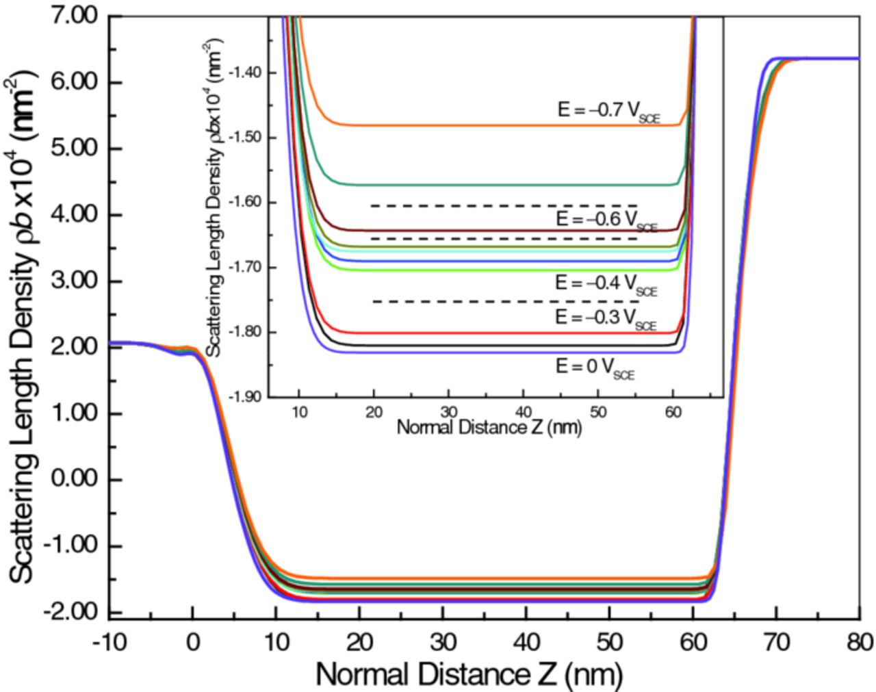
Figure 10. Overlay of the SLD profiles for the Ti thin film electrode at a series of different potentials. The middle region of the SLD profiles, corresponding to the Ti metal layer, is expanded in the inset to highlight changes in the SLD of the metal under cathodic polarization. The dashed horizontal lines indicate the boundaries between regions of behavioral differences.
Figures 11 and 12 plot ρb(Ti) and d(Ti), respectively, as functions of polarization E. Error bars in both are given according to the uncertainties estimated by comparing the models obtained for the as-prepared sample as it was investigated in various geometries (Figure 7). The lack of random fluctuations suggests that the precision (but not necessarily the accuracy) in determining ρb and d is significantly better than indicated by the size of the error bars. These figures, together with Figures 4 and 9, form the basis for our discussion and conclusions.
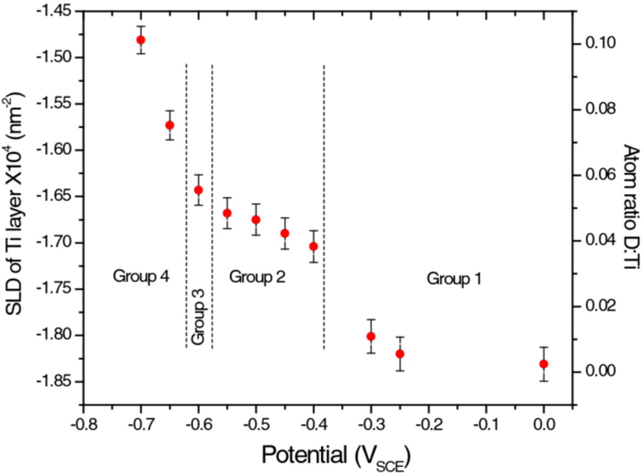
Figure 11. Variations in the SLD of Ti metal together with the ratio of the number of deuterium atoms to the number of Ti atoms in the film as a function of applied potential. As the atomic ratio of D:Ti is calculated based on the SLD change for Ti metal, these values are related by a constant factor. The error bars are based on the maximum experimental error, ±2 × 10⁻⁶ nm−2, as explained in the text. Dashed vertical lines indicate the boundaries between regions of behavioral differences.
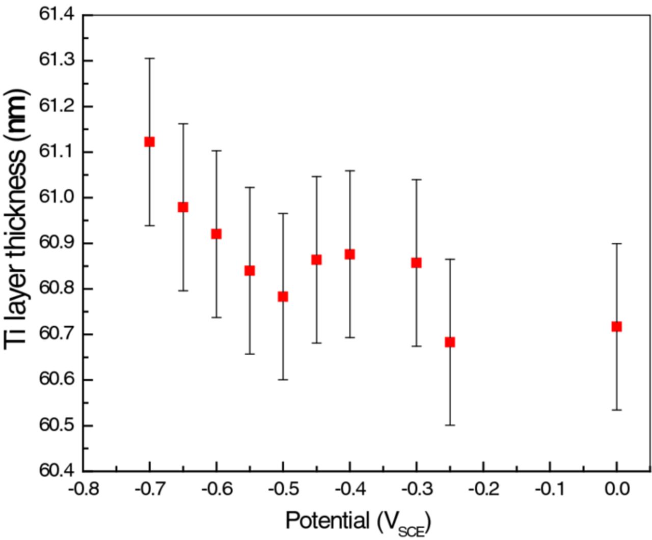
Figure 12. Ti metal layer thickness change as a function of applied potential. The error bars are based on the maximum experimental error, ±0.2 nm, as explained in the text.
Taken together, EIS and NR show the following sequence of changes to the sample:
- (1)For the potentials in Group 1, no significant change is observed. The cell current remained low and was always anodic, if we discount the cathodic spike that occurred immediately after we set the potential (Figure 4). The cell resistance was high and the capacitance low (Figure 9). There is no sign of D infusion to the Ti metal (Figure 11).
- (2)As the potential was set to more negative values (Group 2), the general trend was that the cell resistance decreased while the capacitance increased (Figure 9). At potentials of −0.40 and −0.45 VSCE, the cell current remained cathodic for ∼1000 s after the spike (see Figure 4) before dropping to ∼ zero. For more negative potentials the current was persistently cathodic. The D content in the Ti increased in a step at −0.40 VSCE, and then in smaller increments at the remainder of the Group 2 potentials (Figure 11).
- (3)At −0.60 VSCE the sample went through another abrupt change, marked by a very low cell resistance and a high capacitance (Figure 9). This is the onset of the sharp rise of the D content in the Ti (Figure 11). There is evidence that the Ti layer swelled slightly with the influx of D, but this is based on a trend, instead of the change being larger than the errors (Figure 12).
Based on these results a mechanism to explain the overall behavior of the sample can be proposed. First, we identify the reason for the sharp onset for D ingress at a specific potential (between −0.35 to −0.4 VSCE). For our electrolyte (pH ∼ 6), the equilibrium potential for water reduction to form hydrogen gas and hydroxide ions is about −0.6 VSCE, significantly more negative than −0.4 VSCE. We propose that the underpotential deposition of deuterium occurs in the −0.3 to −0.4 VSCE potential range under these conditions:
![Equation ([4])](https://content.cld.iop.org/journals/1945-7111/160/9/C414/revision1/jes_160_9_C414eqn4.jpg)
where Dads is a surface-adsorbed D atom.37
Existence of a range of potentials where the cathodic polarization is sufficient to reduce H+ to Hads but not for H2 evolution is well documented for Pt and Pd.38 For Pt, underpotential-deposited Hads atoms eventually cover the whole electrode surface, and the cell current falls to zero. On an oxide-covered Ti electrode, however, the Dads atoms may be transported across the oxide if the layer is permeable. Whether transport occurs, and at what rate, will depend largely on the integrity of the oxide layer. To a certain extent, TiO2 layers on regular bulk Ti are highly effective barriers against H ingress. In our case, however, since the underlying Ti is a deposited thin-film containing a high density of grain boundaries and many defects and voids (its SLD is lower than that of bulk Ti), it is conceivable that the oxide is also defective and less effective as a barrier. Consequently, D ingress into the metal may be initiated as soon as Dads atoms are present at the surface.
Close inspection of Figure 4 supports this proposed mechanism. The current spike immediately after we increased the cathodic polarization (Figure 4) is expected, and can be attributed to interfacial capacitative charging. Ignoring surface charging, the cell current observed was exclusively anodic for the potentials in the range from 0 VSCE to −0.3 VSCE. By contrast, at −0.40 and −0.45 VSCE, the current remained cathodic for ∼1000s after the spike, underwent a small jump toward zero, and then fluctuated around zero as a residual current. The residual current is leakage current or due to an electrochemical process that does not involve further loading of D into the underlying metal: otherwise, the D content in Ti would not achieve a steady state. We conjecture that loading of D into the Ti metal takes place within the first 1000s, while the current is cathodic. The two NR scans successively carried out at each potential gave similar results, indicating that the arrival of D within the metallic Ti layer is prompt (i.e., on the order of minutes, not hours) and supporting this proposal.
Additional support for the proposed mechanism, and a more accurate determination of the onset potential, comes from recent work by Zeng et al.12,39 Samples used in that study were 20–30 nm thick TiO2 layers directly deposited onto a Pd substrate (no metallic Ti between the oxide and the substrate). Galvanostatic measurements using a Devanathan cell showed that the H-charging current through the oxide extrapolates to zero at −0.37 VSCE in a plot of potential vs. charging current (Figure 10 in ref. 12). The authors concluded that −0.37 VSCE is the potential where TiO2 becomes transparent to H.
The availability of active electronic current pathways across the TiO2 oxide, which is normally considered an insulator at potentials positive of ∼−0.6 VSCE, has been demonstrated at potentials more positive than ∼−0.6 VSCE by Zhu et al.,17,18 who used scanning electrochemical microscopy to observe the activation of localized electronically conducting sites at which cathodic current could be passed at potentials as mild as −0.04 VSCE. The number and activity of such sites increased as the potential was made more negative. The locations of the active sites were mapped on the surface to demonstrate that they were associated with grain boundaries and triple points in the underlying metal alloys. An influence of alloying element enrichment at grain boundaries, β-phase regions, and intermetallic precipitates on the local oxide conductivity was suggested.
In our case, and in that of Zeng et al.,12,39 the Ti material used to prepare the thin film was high purity Ti, rather than alloy material as used by Zhu et al.,17,18 so we cannot attribute any local activity to the effects of alloying elements or impurities. That may be why we do not observe cathodic currents at potentials positive of −0.4 VSCE, but the fact that we and Zeng et al.,12,39 did observe cathodic currents at potentials more positive than −0.6 VSCE suggests that even without impurities and alloying additions, the presence in the oxide film of electronic defects, vacancies, and disorder at grain boundaries can render the oxide more readily conductive locally.
Taking these observations into account, we suggest that the onset of hydrogen penetration through the oxide and into the metal is controlled by the appearance of surface-adsorbed H (D) on the oxide. The Hads cannot be produced in significant quantities on the oxide surface unless and until the oxide becomes conductive and able to supply the electrons required to reduce water or hydrogen ions to adsorbed atoms (Reaction 5). The development of conductivity, conversion of the TiIV oxide to a mixed TiIII/TiIV oxide, and absorption of hydrogen seem to be all simultaneous consequences of the same conversion process.13 Therefore, once the oxide becomes conductive, at least locally, H atoms can be produced on its surface, then incorporated into the oxide, resulting in its conversion (Reaction 2), followed by H ingress into the underlying metal.
The D content of the Ti metal layer can be determined from the layer SLD, which is a weighted average of the ρb values for the Ti and the D atoms present. At the onset of D uptake, the content of D in Ti reached an atomic ratio of ∼0.04, according to Figure 11, where the atomic ratio, is defined as (number of D atoms)/(number of Ti atoms) in the metal film. From thereon, the D content increased gradually for the remainder of the Group 2 potentials (down to −0.55 VSCE). Since the conditions for reduction of D+ to Dads exist over this entire potential range, this slowdown in D uptake needs an explanation. The critical solubility of H in Ti for hydride formation at room-temperature ranges from 0.002 to 0.004 in atomic ratio H:Ti for bulk metal,40–42 and from 0.06 to 0.07 for evaporated Ti films.43,44 The marked difference between bulk and thin-film is undoubtedly due to morphology: bulk metal grains are tightly packed whereas evaporated thin-films contain substantial voids and cracks. Presumably, as D reaches the metal, hydrides form readily provided the local concentration is above the solubility limit. Subsequently, already formed hydrides separate additional D from the metal surface, leading to a slowdown in further hydride formation: the hydrides formed locally at the base of the D-entry windows provided by defects in the native oxide act as diffusion barriers, effectively blocking the windows and retarding further transport of D atoms into the metal.
This behavior may also account for the discrepancy between the notion that potentials negative of ∼−0.6 VSCE are required for significant and damaging amounts of hydrogen ingress1,5,8,9,11 and the observation of hydrogen penetration at much more positive potentials in this work and recent others.12,17,18,39 If local hydrogen absorption windows at grain boundaries become active, but hydrogen ingress is retarded by hydride "plugs" at their base, then the amount of hydrogen absorbed may appear to be inconsequential (e.g., below detection limit) on a bulk Ti material.
According to Figure 11, a sudden increase in hydrogen content in the Ti film begins at ∼−0.6 VSCE. Ohtsuka et al.13 showed that in neutral solution, cathodic reduction of a TiO2 film does not cause it to dissolve, but induces a change in film composition due to hydrogen absorption (Reaction 2). The amount of hydrogen absorbed is a function of the cathodic potential applied. The redox transformation within the passive oxide (TiIV→TiIII) leads to the availability of multiple oxidation states and a consequent increase in the conductivity of the film. As explained by Nowierski et al.,45 at ∼−0.6 VSCE the oxide film on Ti acts as a wide bandgap semiconductor (with a 3.05 eV bandgap), and a slight deviation from stoichiometry (TiO2−x) transforms the oxide layer into an n-type semiconductor. The combination of oxygen vacancies and interstitial TiIII ions leads to trapping of electrons in an orbital band just below the conduction band edge.14–16 When the TiO2 is polarized to potentials below the flatband potential (∼−0.55 VSCE), redox transformations within the passive oxide (TiIV→TiIII) facilitate electron transfer across the film/solution interface and allow the reduction of protons, an electrochemical process accompanied by absorption of H into the oxide.8,11
Conclusions
The combined use of EIS and in-situ NR techniques has enabled us to reconcile seemingly conflicting literature reports of two key potentials, −0.37 VSCE12 and −0.6 VSCE,13 important in the behavior of a thin-film Ti electrode under cathodic polarization. At the first potential, significant changes in current density, oxide resistivity and capacitance, and the SLD of the Ti are observed. These changes can be attributed to the onset of local oxide conductivity and the underpotential deposition of Dads atoms on the electrode and their entry into the metal through conductive, defective pathways in the oxide. At the second potential, −0.6 VSCE, a marked increase in current density and the D content in the Ti film are observed. The latter potential is recognized as the potential that can render the protective oxide ineffective as a barrier by reducing it from the original TiO2 to TiOOH.13 This is considered the threshold for general hydrogen uptake, which leads to significant hydrogen absorption and embrittlement of industrial Ti structures at potentials negative of −1 VSCE. The former potential, −0.37 VSCE, has not previously been generally recognized as a hydrogen ingress threshold in bulk Ti materials, possibly because it has not led to hydrogen uptake that is sufficient to affect bulk Ti materials.
Acknowledgment
The research presented herein is made possible by a reflectometer jointly funded by Canada Foundation for Innovation (CFI), Ontario Innovation Trust (OIT), Ontario Research Fund (ORF), and the National Research Council Canada (NRC). The Canadian Natural Sciences and Engineering Research Council (NSERC) is acknowledged for additional research support.