Abstract
Previous studies have shown that the electrical activation of a given implanted Al concentration in 4H-SiC increases with the increasing of the post implantation annealing temperature up to 1950–2100°C and different annealing times in the range 0.5–5 min. This study shows that, at 1950°C, the electrical activation of Al implanted in 4H-SiC increases with the increase of the annealing time up to attain saturation for annealing times longer than 22 min. Samples were obtained from the same Al implanted HPSI 4H-SiC wafer with an implanted Al concentration lower than the Al solubility limit in 4H-SiC at the annealing temperature of 1950°C. The annealing time was varied in the range 5–40 min.
Export citation and abstract BibTeX RIS

This is an open access article distributed under the terms of the Creative Commons Attribution Non-Commercial No Derivatives 4.0 License (CC BY-NC-ND, http://creativecommons.org/licenses/by-nc-nd/4.0/), which permits non-commercial reuse, distribution, and reproduction in any medium, provided the original work is not changed in any way and is properly cited. For permission for commercial reuse, please email: oa@electrochem.org.
Nowadays, silicon carbide (SiC) components have gained a significant position in the power electronic market among the low-loss, high-power and high-frequency devices capable of operating in harsh conditions.1–4 Large area 4H-SiC epitaxial wafers, from 4 to 6 inches diameter, are commercial available3 and foundries offering SiC wafer processing can be found.5 Nevertheless, industrial and academic research are still very active both on the side of the SiC material growth and on that of the SiC wafer processing. This study deals with the SiC processing and in particular with the electrical doping of SiC by ion implantation.
Ion implantation is a consolidated technology for obtaining a desired doping depth profile in selected regions of a semiconductor wafer during the fabrication of planar electronic devices. In the case of SiC devices, an alternative technology has been developed for obtaining the doping of selected regions while preserving a planar wafer surface. Such a technology is the embedded epitaxial growth.6 Anyway, the cost of this technology and the difficulty of its control are so high that embedded epitaxial growth is limited to the fabrication of device channel regions while for the device termination regions or for the test of new doping profiles, ion implantation remains the preferred technology.
The electrical doping of a crystalline semiconductor by ion implantation requires a mandatory post implantation thermal treatment. This treatment aims to recover the disorder in the semiconductor lattice produced by the ion bombardment and to favor the contemporaneous allocation of the implanted atoms in substitutional lattice sites where they act as electrically active dopant. In the case of SiC, in particular for implanted Al in 4H-SiC, there are still open issues related to the understanding of the post implantation annealing effects on both implanted and unimplanted SiC materials. As an example, it can be mentioned the fact that by increasing the post implantation annealing temperature up to 1950–2100°C, with different annealing times in the range 0.5 −5 min, the electrical activation of Al implanted in 4H-SiC is improved,7–9 but, the role of the annealing duration at such high temperatures has never been studied. While for annealing temperatures below 1800°C, such a role has been studied and contradictory results have been obtained.10–13 Therefore, further investigations appear as necessary for understanding the effect of the duration of the post implantation annealing on SiC.
It is worthwhile to recall that, in principle, the maximum expected electrical activation for a given implanted species in a semiconductor material cannot exceed the value corresponding to the solid solubility of the implanted species in the semiconductor lattice at the temperature of post implantation annealing. Generally, solid solubility increases with the increase of the processing temperature. This explains the improving of the electrical activation of a given implanted dopant species in SiC with the increase of the post implantation annealing temperature. Nevertheless, to the best of these authors knowledge, the concentration of the implanted dopant species in 4H-SiC has often overcome their solid solubility values at the used annealing temperature; examples can be found in Refs. 9 and 13. This is an experimental configuration that should be avoided because it favors the formations of both dopant precipitates and structural extended defects14–16 that may affect the carrier transport in the implanted layer.16 The solid solubility limits of the p-type doping species B and Al in 4H-SiC have been measured in the temperature range 1700–2000°C and they are published in Ref. 17 and in Ref. 18, respectively.
Al is generally preferred to B when elevated p-type doping levels are desired. In fact, Al has an higher solid solubility in 4H-SiC at the temperatures necessary to obtain a significant electrical activation. For example, the Al solubility in 4H-SiC at 1900°C is 2 × 1020 cm−318 while that of B is 5 × 1019 cm−3.17 Al has also a lower thermal ionization energy in 4H-SiC than B, about 200 meV19 against about 600 meV.20 Moreover, the Al ionization energy shows an important dependence on the Al acceptor concentration.21 In the case of identical B and Al acceptor concentrations, such differences favor a higher p-type conductivity in the Al case because of its lower partial ionization at any sample temperature. Last but not least, a reason for preferring Al to B, is that Al is almost immobile during post implantation annealing while B not at all.22
This works is a study on the relevance of the annealing time during the electrical activation of Al implanted in 4H-SiC at 1950°C annealing temperature. In this study the implanted Al concentration has been kept almost equal to 1 × 1020 cm−3 that is lower than the Al solubility in 4H-SiC at the annealing temperature of 1950°C.18 Moreover, to avoid the activation of phenomena favored by temperatures lower than 1950°C, a fast heating rate has been used. At the same time, for quenching the annealing process at the end of the time spent at 1950°C, a fast cooling rate has been used too.
Experimental
A High Purity Semi-Insulating (HPSI) 8° off-axis <0001> 4H-SiC wafer was Al+ implanted at 400°C with various doses and energy to obtain an almost box shaped Al depth profile, 1 × 1020 cm−3 high and about 1.3 μm thick next to the wafer surface. Ion implantation was performed by using a Tandentron 1.7 MV accelerator (High Voltage Engineering Europa B.V.), equipped with a 4 inches wafer holder. A thick SiO2 film was deposited on the wafer before implantation. This film has the function to decrease the ion kinetic energy so that a flat Al depth profile next to the wafer surface can be obtained. After the implantation, the wafer was diced in 5 mm × 5 mm pieces. The SiO2 film was accurately removed in a hydrofluoric bath. Immediately after, a resist film was spun on the implanted surface of each sample. This film was transformed in a carbon layer (C-cap) by a pyrolysis at 900°C for 2 min in forming gas.23
Post implantation annealing processes were performed in high purity Ar ambient. The samples were inside an inductively heated graphite box (crucible). In such a system, crucible heating and cooling are controlled by regulating the power of the radio frequency generator. The maximum heating rate of our setup is 40°C/s, while the faster cooling transient is determined by the thermal inertia of the crucible once the generator is switched off. The temperature of the crucible is measured by an optical pyrometer. All the samples of this study were treated with annealing temperature, heating rate and cooling cycle constant and equal to 1950°C, 38°C/s, exponential with 65 s time constant, respectively. The latter corresponds to a time t dependence of the cooling temperature T given by the equation T = 1950 exp[(t0-t)/65] with t0 (time at which T starts to decrease) and t expressed by "second" unit. All that corresponds to about 1 min (0.1 min spent above 1600°C) to reach the annealing temperature, and to about 5 min (0.2 min spent above 1600°C) to cool down to RT after annealing. To the best of these authors experience, 1600°C is the minimum annealing temperature for measuring a significant electrical activation of implanted Al in 4H-SiC. Moreover, temperature overshoot and time to reach temperature stationarity were 15°C and 20 s, respectively. Four samples with different annealing times of 5–10–25–40 min were processed. After annealing, the C-cap was removed by a 850°C/15 min dry oxidation process.
van der Pauw (vdP) devices were obtained by forming triangular Ti(80 nm)/Al(350 nm) ohmic contacts on the four corners of the annealed specimens. These contacts were alloyed 1000°C/2 min in vacuum.
The root mean square (rms) surface roughness, not shown in this work, was measured on virgin and annealed materials, the latter after C-cap removal. This parameter was found 0.2 nm and ≤ 5 nm for the virgin sample and the sample of longer annealing time, respectively. This is an expected trend.
The Al depth profiles after annealing were measured by Secondary Ion Mass Spectrometry (SIMS) by using a Cameca IMS-4f spectrometer with an 8 keV O2+ primary ion beam.
Four point sheet resistance and Hall effect measurements on the van der Pauw devices were performed in vacuum at different temperatures in the range 30–680 K. Two different set-ups, equipped with magnets of different intensity, were used for measurements above (1 T magnet) and below (0.8 T magnet) room temperature (RT). Measurements of the same sample were taken during heating and during cooling, moreover they were repeated at distance of time. The spread of all the data at a given temperature was less than one percent. Due to the non-negligible dimensions of the contacts with respect to the device size, proper correction factors were applied to the results of both sheet resistance and Hall coefficient measurements.24 To convert the Hall data in drift data the Hall factor rH of Ref. 25 for holes in 4H-SiC has been used. It is worthwhile to remember that this factor is temperature dependent rH(T). In Ref. 26 it has been shown that this rH25 is valid for Al acceptor densities in 4H-SiC going from 1.8 × 1015 cm−3 to 1.1 × 1020 cm−3.
Results
Fig. 1a shows the SIMS Al depth profiles of the 5 min and 40 min annealed specimens. The differences between these two Al depth profiles are consistent both with the uncertainty of the SIMS measurements and with differences in the thickness of the SiO2 film used as stopping power of the ion energy during the implantation process. Every other sample of this study had an Al depth profile overlapping with those of Fig. 1a. Fig. 1b is a schematic drawing of the Al depth profiles of Fig. 1a. The Al depth profiles show the scheduled 1.1 × 1020 cm−3 plateau about 1250 nm thick but with a significant depletion around 700 nm. Such a depletion is the consequence of an error in the performed implantation process. Fortunately, such an error does not hamper the possibility to perform the desired study (see the Discussion section).
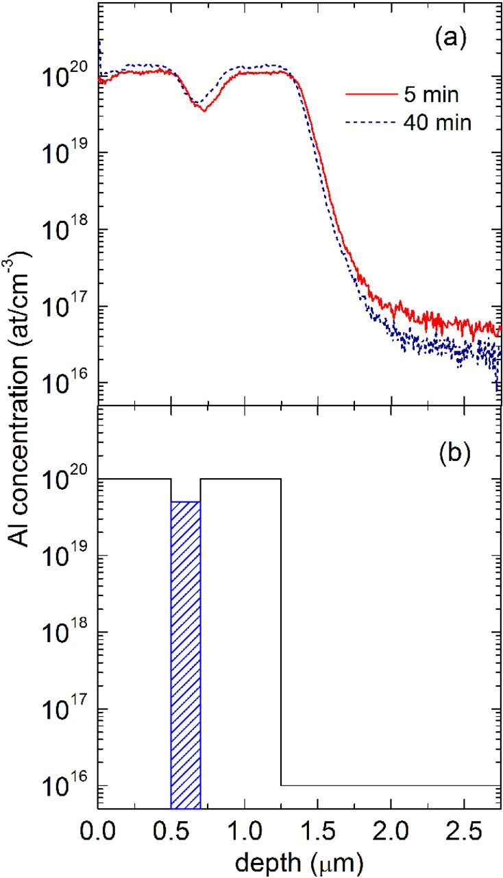
Figure 1. (a) SIMS Al depth profiles of the 5 min and 40 min annealed 4H-SiC samples. (b) Schematic representation of the Al depth profiles of (a).
Fig. 2a shows the Arrhenius plot of the temperature dependence of the sheet resistance of all the samples of this study. Fig. 2b is the enlarged view of the high temperature region of Fig. 2a. This figure shows that at high T the sheet resistance values of the Al implanted layer of this study decreases with the increasing of the annealing time and attains saturation for annealing times longer than 25 min. No dependence of the sheet resistance curves on the annealing time is evident at low T. Each curve of Fig. 2a features two almost exponential trends, at low and at high temperatures, as for a carrier transport that is thermally activated over the whole T interval, but with two different thermal activation energies, and thus two different mechanisms involved, depending on T. Thermal activation energy values in the high T region attain hundreds of meV while those in the low T region, tens of meV. Moreover, at high T, these values decrease with the increasing of the annealing time, varying from 116 meV for 5 min annealing to 107 meV for 25–40 min annealing. At low T a single thermal activation energy of about 20 meV accounts for all the curves.
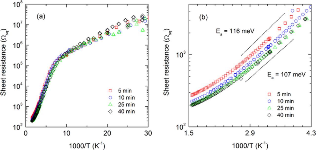
Figure 2. (a) Temperature dependence of the sheet resistance of the Al implanted HPSI 4H-SiC samples of this study after 1950°C annealing, 5−10−25−40 min long (see inset). (b) Enlarged view of the high temperature region of (a). The dimension of symbols includes the measurement error bars.
The RT sheet resistance values of Fig. 2 are plotted versus the annealing time in Fig. 3. Two straight lines interpolate the 5 min and 10 min data, and the 25 min and 40 min ones. The cross point between these straight lines falls at ≈ 12 min. This value is an estimation of the minimum time spent at 1950°C for achieving the lowest p-type sheet resistance for the Al implanted layer of this study.
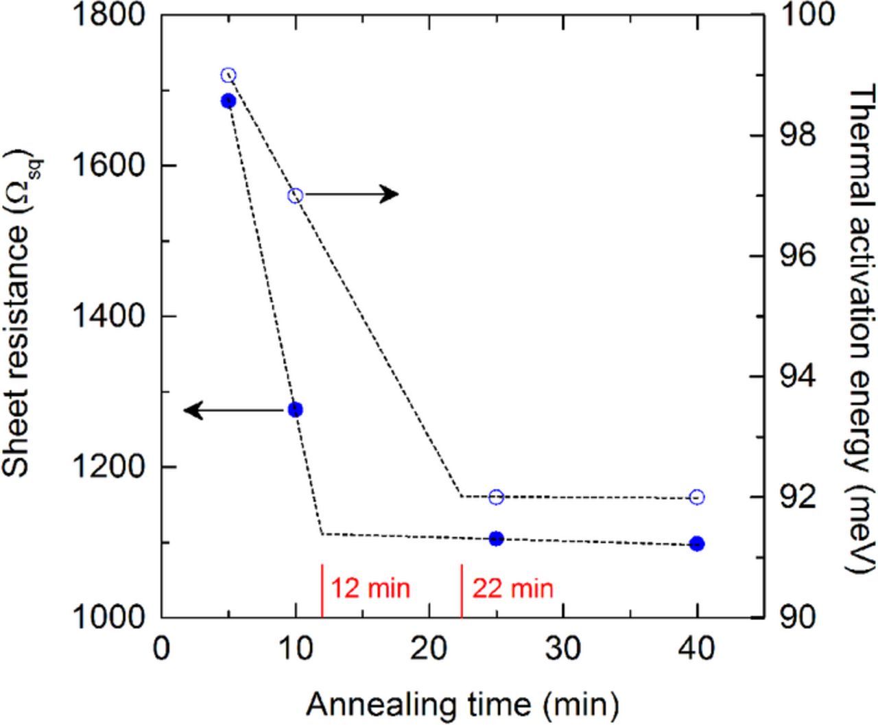
Figure 3. Room temperature values of sheet resistance (●) and acceptor ionization energy (◯) of the samples of this study after post implantation annealing at 1950°C (see text) and different annealing times. Dashed straight lines interpolates the decreasing and the saturated data (see text). The cross point between these two trends is 12 min and 22 min for sheet resistance (●) and acceptor ionization energy (◯), respectively.
Fig. 4a shows the temperature dependence of the ratio rH(T)/[e RH(T)], i.e. the ratio between the Hall factor rH(T) and the product of the measured Hall coefficient RH(T) times the elementary charge e. This quantity, that has the dimension "cm−2", in the case of homogeneously doped layers, is the drift hole area density of the measured layers. In the Discussion section it will be explained why, in the case of the Al implanted layers of this study, the quantity plotted in Fig. 4a can be equal to the effective carrier area density in the layer. Fig. 4b is an enlarged view of the high temperature region of Fig. 4a. With the increase of the annealing time, the curves of Fig. 4a attain higher values, up to reach saturation values for annealing time above 25 min. In the low T region, the temperature dependence of the curves of the10–25–40 min samples of Fig. 4a show a minimum, while in the high T region all the curves of Fig. 4a show an exponential trend. These latter have activation energies that decrease from 99 meV down to 92 meV with the increasing of the annealing time from 5 min to 25 min (see Fig. 4b). Above 25 min, thermal activation energies equal that of the 25 min specimen. These values have been plotted in Fig. 3 as a function of the annealing time. The cross-point between the two straight lines that interpolate the 5–10 min data and the 25–40 min ones falls at ≈22 min. This time is the minimum time spent at 1950°C for achieving the lowest activation energy in the high T region of the temperature dependence of the carrier area density in the samples of this study.
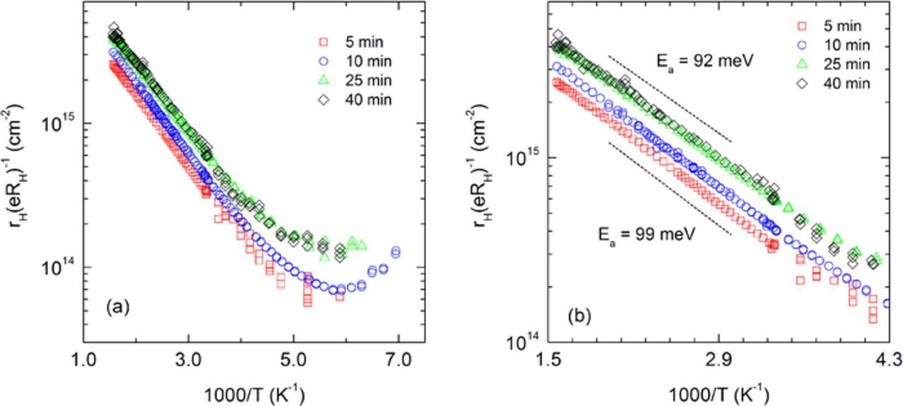
Figure 4. (a) Temperature dependence of the drift hole area density of the Al implanted layer of the 4H-SiC samples of this study (see text). (b) Enlarged view of the high temperature region of (a). The dimension of symbols includes the measurement error bars.
The drift carrier mobility in the Al implanted layers of the samples of this study has been obtained as the ratio between the Hall coefficient RH(T) corrected by the Hall factor rH(T)25 and the measured sheet resistance. The computed curves are shows in Fig. 5, where, for comparison, straight lines with T 3/2 and T−3/2 dependences are also shown in Fig. 5. The former is the expected trend when the carrier mobility is dominated by the Coulomb interaction of carriers with ionized impurities. The latter is the expected trend when carrier mobility is dominated by lattice phonons scattering. All the experimental curves of Fig. 5 exhibit a broaden maximum around 350 K, and decrease abruptly than T3/2 and smoothly than T−3/2 below and above 350 K, respectively. Fig. 5 shows also that the mobility curves of the 5 min and 10 min samples almost overlap, and that the same is true for the curves of the 25 min and 40 min samples; at the same time, the values of the former curves are higher than those of the latter.
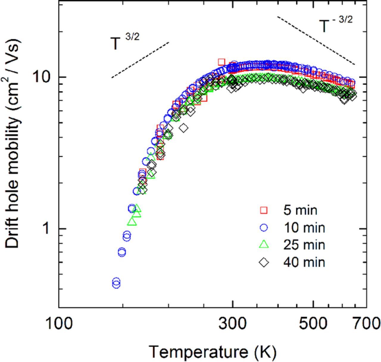
Figure 5. Temperature dependence of the drift hole mobility in the Al implanted layer of the 4H-SiC samples of this study (see text). For comparison, dashed lines show the T3/2 and T−3/2 trends that correspond to the expected temperature dependence for mere ionized impurity scattering and mere phonon scattering, respectively.
Discussion
The differences in the Al depth profiles of the SIMS spectra of Fig. 1 can be attributed to the poor homogeneity of the processed samples as said in the Experimental part. Moreover, till present we have measured neither a profile shift nor a dopant in/out diffusion for implanted Al in 4H-SiC. Based on all that, we say that the SIMS measurements of the Al implanted 4H-SiC samples of this study (see Fig. 1a) point out that the Al depth distribution is not significantly affected by the duration of the annealing time.
The SIMS measurements show also that the performed implantation process was not the scheduled one because the desired Al plateau has a deep at about half of its thickness. This dopant distribution results in a non-uniform carrier density that prevents the possibility to derive the material resistivity and the drift carrier density of the implanted layer from a simple multiplication of the implanted layer thickness times the measured sheet resistance and times the measured Hall coefficient (once corrected by the Hall factor), respectively. Nevertheless, a comparative study on the effect of the post implantation annealing time is still possible and reliable as far as the mere sheet resistance and the Hall coefficient data are compared because identically implanted samples have been used for each annealing time experiment. Moreover, the measured Hall coefficients RH are still indicative of the integral of the free carriers in the corresponding implanted layers, like in homogeneously doped layer because it is the result of parallel electrical conductions. In fact, in the samples of this study the carrier transport takes place through the parallel channels, made of the SiC material with different dopant concentrations (see Fig. 1b), each channel having its own carrier density and carrier mobility. However, being the doping fluctuations across the layer thicknesses quite limited, 1 × 1020 cm−3 against 5 × 1019 cm−3 (see Fig. 1b) the corrections to hole density and mobility due to the mixed conduction effects are expected to be not very significant and in practice independent on the temperature. Therefore, the values of the reciprocal of RH divided by the elementary charge taken as a function of the temperature are still indicative of the Hall carrier density in the implanted and annealed layer, and can be treated as an effective Hall area density having the same temperature dependence of the real one. In addition, such effective Hall data can be converted to drift data using the Hall factor curve rH (T) of Ref. 25, as mentioned in the Experimental section. Soon after, it will be shown that the carrier transport in the Al implanted layers of this study features two different mechanisms, one dominant over the other depending on the temperature region. It is worthwhile to recall that the use of the Hall factor rH has been proved necessary for the analysis of data relative to the transport into valence band states, whereas it is questionable for data relative to transport between impurity states.27 Nevertheless, in this study, the Hall factor rH has been applied to all the our data because, as it will become evident in the following, the main quantitative remarks will concern the temperature range where the transport takes place through valence band states.
The temperature dependencies of the sheet resistance (Fig. 2a), of the drift hole area density (Fig. 4a) and of the mobility (Fig. 5) for every annealing time feature a carrier transport dominated by extended states in the valence band at high T and by localized states in an impurity band at low T. The interpretation of the different exponential regions of the sheet resistance curves (see Fig. 2a) in the frame of the Miller and Abrahams model28 supports the previous statement. The fact the curves of the drift carrier density (see Fig. 4a) show a minimum while the corresponding carrier mobility curves decrease with a trend steeper than that of the carrier freeze-out into the Al acceptors (see Fig. 5), points out the formation of a dopant impurity band. The exponential trends of the high T region of the sheet resistance (Fig. 2a) and of the drift hole area density (Fig. 4a) curves, together with their thermal activation energies, supports the statement that at high T the carrier transport takes place in the extended states of the valence band. In fact, the thermal activation energies are of the order of 100 meV. This value is very close to the thermal ionization energy of Al in 4H-SiC when the acceptor concentrations is in the range 1018–1020 cm−3.21,26 The transition from a dominant valence band carrier transport to a dominant impurity band carrier transport takes place in a broad temperature region around 150 K. This can be deduced from the broad minimum of each curve of drift area density (Fig. 4a) and the smooth change of slope in each curve of sheet resistance (Fig. 2a).
The thermal activation energy for carrier transport into the impurity band has been obtained by the sheet resistance data at low T (Fig. 2a) and it amounts to about 20 meV. This value is congruent with a transport mechanism through a nearest neighbor hopping between occupied and unoccupied Al acceptor sites.29–31 The formation of an impurity band for every annealing time in the range 5–40 min confirms the high efficiency of the post implantation annealing at 1950°C in the case of Al implanted in 4H-SiC but it does not answer to the question how relevant is the annealing duration at such a high annealing temperature. This answer can be found by considering the high T region of both the sheet resistance (Fig. 2b) and the drift hole area density (Fig. 4b) curves. This high T region goes from 230 K to 680 K.
Above 230 K and up to the maximum temperature of measurements of 680 K, all the drift hole area density curves (Fig. 4b) are exponential while the sheet resistance ones (Fig. 2b) are exponential up to 500 K and show a smother temperature dependence above this temperature. It is worthwhile to recall here that the temperature dependence of the of the drift hole area density is determined only by the temperature dependence of the partial ionization of the Al acceptor, while the temperature dependence of the sheet resistance is due to both to this latter and the temperature dependence of the mobility (Fig. 5). The sheet resistance curves show that 500 K is the temperature limit above which the sheet resistance trend is dominated by the partial ionization of the Al acceptors. In such a case it may be expected that the exponential regions of corresponding sheet resistance and drift hole area density data, i.e. of curves of equal annealing time, had identical thermal activation energies, and that these values were equal to the Al thermal ionization energies in 4H-SiC. All that has been found only partially true. In fact, the thermal activation energies of the sheet resistance curves are always lower than those of the corresponding drift hole area density curves. The former are in the range 107–116 meV and the latter in the 92–99 meV one. All these values are reasonable as Al thermal ionization energies in 4H-SiC, but those obtained from the drift hole area density data have to be selected as the proper ones because the temperature dependence of this parameter is affected only by Al partial ionization. A common feature to both the families of the thermal ionization energies is a decrease of their values with the increasing of the annealing time down to saturation for times longer than 25 min.
The absence of a homogeneous Al dopant distribution in the implanted layer (see Fig. 1) hampers the possibility to use the simulation tools previously developed in Ref. 26 to derive the Al thermal ionization energy, the Al substitutional fraction and the compensation level in each sample of this study, i.e. for each annealing duration. In spite of that, the thermal activation energy of the 5 min curve of Fig. 4b is very close to that obtained in previous studies for 1.1 × 1020 cm−3 Al implanted 4H-SiC after 1950°C/5 min annealing,26 more precisely 99 meV in this study against 102 meV previously published.26 The parallel conduction in adjacent layers of almost homogeneous dopant concentration (see schematic Al depth profile of Fig. 1b) or a different compensation level may account for such difference. As the variations in the slopes of the curves of Fig. 4b significantly overcome such a difference we say that the obtained values are reliable and not significantly affected by errors due to the not homogeneous dopant depth profile.
Semiconductor materials doped by ion implantation are always compensated semiconductor. In such materials, the dopant effective ionization energy decreases with the increasing of the doping level and/or the increasing of the compensation level,21,29 whereas the resistivity decreases and the drift carrier density increases with the increasing of doping level and/or the decreasing of the compensation ratio. While keeping in mind that sheet resistance and carrier area density differ from resistivity and carrier density only for a constant multiplying factor given by the thickness of the implanted layer, we can interpret the results of our study in the light of the recalled knowledge about compensated semiconductors. In the samples of this study, with the increasing of the annealing time, the sheet resistance curves gain lower values down to saturation while the corresponding drift area density curves gain higher values up to saturation and the Al thermal ionization energy decreases down to saturation. All that agrees with the hypothesis of an increasing of the Al acceptor concentration up to saturation with the increase of the annealing time.
Also the high T region of the mobility curves of Fig. 5 can be used to perform hypotheses about the effect of the increasing of the annealing time on the electrical activation and on the compensation in the samples of this study. In this region the hole mobility curves have values that decrease going from 5–10 min annealing time to 25–45 min. This latter may indicate an increased scattering by charged or neutral centers.26,32 Al acceptors and carrier traps may be charged scattering centers while the not substitutional Al atoms may be neutral scattering centers.32 Our previous studies have shown that with the Al implanted concentration and the annealing temperature used in this study, a neutral scattering contribution to the hole mobility is negligible.26 Thus the decrease of the mobility values with the increase of the annealing time can be attributed to an increased scattering by charged centers. With the increasing of the annealing time the density of the Al atoms in substitutional position may increase or remain constant. Supposing fixed the compensation level, this would correspond to an increasing or to a stable value of charged scattering centers with the increasing of the annealing time. The compensation levels may decrease or remain constant with the increasing of the annealing time. Supposing a fixed Al acceptor concentration and compensation performed by all occupied traps, this would correspond to decreasing or stable value of charged scattering centers with the increasing of the annealing time for acceptor like traps, while to a stable value of charged scattering centers for donor like traps. Thus only an increasing of the Al acceptor concentration with the increasing of the annealing time accounts for the mobility decrease with the increasing of the annealing time. This conclusion agrees with that obtained through the analyses of the sheet resistance and drift hole area density data.
The saturation of the values of the transport data with the increasing of the annealing time shows that it exists a minimum annealing time at 1950°C for obtaining the higher Al electrical activation in the samples of this study. This time has been obtained by the interpolations of the Al thermal ionization energies of the samples of this study that are shown in Fig. 3. The cross point between these two lines allow us to say that this minimum time is about 22 min.
Fig. 3 shows also that the minimum time for obtaining the better Al electrical activation is longer than the minimum time necessary to obtain the lower sheet resistance value for the same Al implanted 4H-SiC layer, i.e. 22 min against 12 min. Such a difference may show the way for a reasonable trade-off aimed to reducing the thermal budget of SiC device manufacturing, that is the minimization of the sheet resistance instead of the maximization of the electrical activation of the implanted dopant.
Conclusions
This study shows that the electrical activation of Al implanted in 4H-SiC with concentrations lower than its solubility values at the annealing temperature increases with the increasing of the annealing time up to saturation. In the particular case of this study, 1 × 1020 cm−3 Al implanted HPSI 4H-SiC, 400°C implantation temperature, and 1950°C post implantation annealing temperature, the minimum time to obtain the maximum Al electrical activation is about 22 min.
Acknowledgments
Michele Sanmartin, Michele Bellettato, Filippo Bonafè, Dr. Emanuele Centurioni, Dr. Ivan Elmi, and Dr. Pietro De Nicola, are warmly acknowledged for their support during sample processing. Salvatore Vantaggio and Maurizio Puzzanghera are warmly acknowledged for their support during electrical measurements.