Abstract
Rapid decay of silicon anodes during lithiation poses a significant challenge in application of silicon as an anode material in lithium ion batteries. In situ Raman spectroscopy is a powerful method to study the relationship between structural and electrochemical data during electrode cycling and to allow the observation of amorphous as well as liquid and transient species in a battery cell. Herein, we present in situ Raman spectroscopy on high capacity electrode using uncoated and carbon-coated silicon nanowires during first lithiation and delithiation cycle in an optimized lithium ion battery setup and complement the results with operando X-ray reflection diffraction measurements. During lithiation, we were able to detect a new Raman signal at 1859 cm−1 especially on uncoated silicon nanowires. The detailed in situ Raman measurement of the first lithiation/delithiation cycle allowed to differentiate between morphology changes of the electrode as well as interphase formation from electrolyte components.
Export citation and abstract BibTeX RIS

This is an open access article distributed under the terms of the Creative Commons Attribution 4.0 License (CC BY, http://creativecommons.org/licenses/by/4.0/), which permits unrestricted reuse of the work in any medium, provided the original work is properly cited.
Lithium ion batteries (LIBs) have been a subject of intense research since its first conception more than 25 years ago.1 In a path to establish a fully electric car comparable to combustion engine-powered vehicles, LIBs continue to be the most advanced and the most promising option.2–4 The development of high capacity electrode materials is among the most critical limiting factor to the progress of the next generation LIBs for electric vehicles. In the case of anode material, silicon has the highest theoretical capacity (4200 mAh/g), which is ten times more than the capacity of currently used graphite (370 mAh/g).5,6 However, silicon anodes show dramatic volume change during lithiation and delithiation, which leads to pulverization of anode material, unstable solid electrolyte interphase (SEI) formation and subsequent battery failure.7–10 In order to solve these problems, nanostructured anode materials (e.g. nanoparticles, porous nanoparticles, nanowires, double-walled nanotubes) have been extensively studied.11–15
A lot of experimental research techniques have been developed in order to better understand and further improve electrochemical performance of electrode materials in rechargeable lithium batteries. In situ Raman spectroscopy is one of the most advanced methods for studying structure-property relationships during battery operation.16–18 It has been widely used to study LIBs with graphite anodes.19–21 However this technique is challenging for silicon anodes due to the formation of a thick SEI layer on the active material surface, which tremendously decreases the desired information depth and results in a significant contribution of the background fluorescence. This issue additionally coincides with a reduced intensity of the Raman signal due to the amorphous nature of silicon lately at low states of discharge or higher cycling numbers where highest amorphization rates are observed. Higher laser power and longer exposure times are required to obtain the necessary signal quality, which may lead to sample irradiation damages and the unwanted evaporation of the electrolyte solvents with pressure increase inside the cell.
Despite these difficulties, in situ Raman spectroscopy for silicon anodes has been attempted by some research groups. Holzapfel et al. reported in situ Raman microscopy on a composite electrode based on the mixture of nano silicon and small graphite particles.22 They observed a complete disappearance of the crystalline silicon signal upon the first lithiation, which was attributed to the silicon amorphization. The main graphite bands were detected with spectral characteristics of an intercalation reaction. Nanda et al. also reported the complete disappearance of the crystalline silicon signal upon the first lithiation of a Si/C composite anode based on microcrystalline silicon homogeneously dispersed on a carbon matrix.23 However, the amorphous silicon signal was not detected during the first delithiation due to a low signal-to-noise ratio. Moreover, neither study provided any observations of electrolyte decomposition, SEI or Li-Si alloy formation in the Raman signals. Hy et al. performed the first in situ surface enhanced Raman spectroscopy (SERS) study of a silicon dioxide layer on a gold nanoparticle anode.24 They observed a drop in the intensity of the signal at the position of crystalline silicon with decreasing voltage, but not its complete disappearance. An amorphous silicon band and SEI species formation were also detected. Zeng et al. used in situ Raman microscopy to investigate the lithiation-induced stress in silicon nanoparticle anodes.25 They reported on a high remaining intensity of the first-order crystalline silicon peak in the first four hours of investigation during initial lithiation followed by a sharp decrease in the sequel. This result is consistent with the typical electrochemical behavior of silicon at the beginning of the lithiation where almost no structural change is observed. Therefore, the previously observed quick and complete disappearance of the crystalline silicon signal could be due to the formation of the thick SEI film blocking the silicon signal and not due to the amorphization.25 Zeng et al. also detected a nearly constant Raman signal mainly induced by the electrolyte, but no further details were provided on the formation of SEI species, Li-Si alloys or on the first delithiation reactions.25
Although in situ Raman spectroscopy has been previously performed for the silicon anodes, no study is known which has shown full high intensity Raman spectra with detailed interpretation of the structural and electrochemical changes during the first cycle of the battery. In this study, we present in situ Raman spectroscopic experiments on a silicon nanowire (SiNW) anode material and compare the results to the same structure with carbon-coated SiNWs. We prove that the reduction of the crystalline Si Raman signal is attributed to the formation of a thick SEI layer on the nanowire surface. Additionally a previously unknown Raman signal at 1859 cm−1 is measured which is assigned to a compound of the SEI especially on the uncoated SiNW surface. The Raman experiments are supported by operando synchrotron X-ray transmission diffraction measurements of similar samples to clearly separate structural changes in the silicon nanowires from the observed Raman results.
Experimental Methods
Electrode preparation
Carbon fiber networks (Sigracet GDL 25AA, SGL Carbon) were used as a three-dimensional conducting substrate and current collector for the SiNW growth (Figure 1). Thereon Au nanoparticles were deposited as catalyst seeds by an adapted galvanic pulse plating process. The gold deposition was carried out in a three-electrode setup, consisting of the carbon fiber network as working electrode, a platinum-coated titanium mesh (METAKEM) as counter electrode and a saturated silver-silver chloride electrode (SSE) as reference electrode (SE11, Sensortechnik Meinsberg). The electrolyte consisted of 1 mM tetrachloroauric acid HAuCl4 (99.99%, Alfa Aesar) in 0.5 M sulfuric acid (98%, Carl Roth) and 1 g/L ammonium dodecyl sulfate ADS (30% solution, Fluka). For pulse plating, a potentiostat / galvanostat IMP 83 PC – 10 (Jaissle Elektronik GmbH) in combination with a waveform generator AFG 3251 (Tektronix) was used. For deposition, cathodic pulses of φ = −0.7 VSSE and t = 10 ms and anodic pulses of φ = 0.9 VSSE and t = 90 ms were repeated alternatingly for ttotal = 10 s.
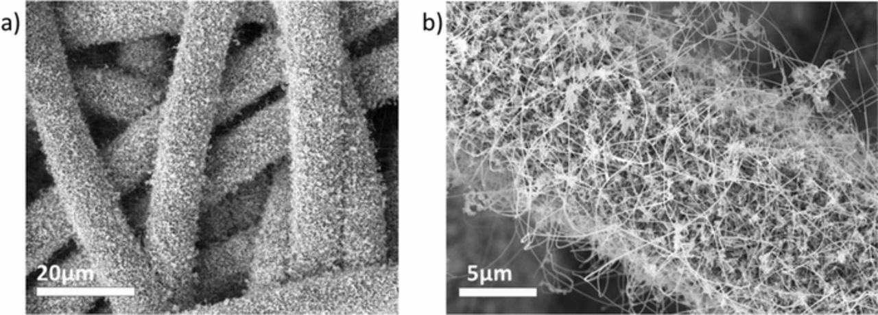
Figure 1. SEM (in-lens detector) images for silicon nanowires on carbon fiber network. a) Low magnification image of the mesh which is made of fibers with 10 μm diameter. b) The (carbon-coated) SiNWs are uniformly grown on the fibers.
The SiNWs were conformally and densely grown on the as prepared Au nanoparticle covered fiber substrate (Figure 1b) via the vapor liquid-solid (VLS) mechanism.26 The SiNWs were grown in a chemical vapor deposition (CVD) vacuum furnace (LPCVD PEO603, ATV GmbH) at 430°C with diluted SiH4 (process pressure 150 mbar, 60 min growth time, precursor gas H2:SiH4; 200:40 sccm).27 Some of the samples were subsequently coated with conductive pyrolytic carbon in the same furnace at 820°C (process pressure 100 mbar, precursor gas C2H4:N2 60:200 sccm) and a deposition time of 20 min, corresponding to a thickness of approximately 20 nm. Similarly prepared carbon layers showed an extremely homogenous deposition at aspect ratios of more than 1:430 in deep trench capacitors.28 The gas purities of H2, N2, SiH4 and C2H4 (Air Liquid) are 6N, 6N, 4N and 4N5 respectively. The thickness of the carbon layer was measured using deep ultraviolet spectroscopic ellipsometry (SENTECH SE 800 DUV 190–980 nm, 1 mm spot size) on a Si wafer piece simultaneously coated together with the SiNWs. The resistivity of the pyrolytic carbon layer was 3mΩcm.
Battery assembly and in situ Raman measurement setup
In situ coin cells were used to perform the spectro-electrochemical investigation of the carbon-coated and uncoated SiNW anodes without any binder polymer and conductive additive. Figure 2a shows a schematic setup of the half-cell setup and Figure 2b the assembled SiNW/Li coin cell. Figure 2c shows an optical image taken from the Raman microscope into the battery cell. The cell was assembled in an Argon filled glove box using LP30 electrolyte with ethylene carbonate (EC) and dimethyl carbonate (DMC) as solvent in the ratio 1:1 (v/v) and 1M Lithium hexafluoro-phosphate (LiPF6) as conducting salt. The separator was a highly porous glass fiber nonwoven (Whatman, Ø 1.27 cm, thickness 180 μm), also soaked with LP30 electrolyte (EC/DMC 1:1 (v/v), 1M LiPF6, Merck) as electrolyte. The battery housing consisted of a modified coin cell with a quartz window (60 μm thickness) allowing a spectroscopic observation from the back side of the fiber based SiNW electrode. A perforated copper foil was added as current collector to ensure a stable electrical contact to the back frame.

Figure 2. In situ test cell for Raman investigation. a) The setup of the SiNW electrode for the Raman measurement allows an observation of the electrode from the back side. b) The quartz window of the assembled coin cell. c) View from the Raman microscope into the cell. The fiber network is visible, brighter parts are deeper fibers within the electrolyte. For optimal signal with less noise and electrolyte signal, an electrolyte covered fiber with nanowires touching the quartz window is used for in situ characterization.
The batteries were cycled during Raman measurement using a Biologic SP50 potentiostat. Galvanostatic cycling with potential limitation (GCPL) was performed between 1.2 V and 0.01 V with 0.2 mA constant current. During cycling the continuous in situ Raman measurements were done with an excitation wavelength of 514 nm using an Ar ion laser (Reliant 150 Select, Laser Physics) within a Raman scattering microscope (Renishaw Invia) and a nominal power of 2 mW at the illuminated battery area, 20 s exposure time and 4 and 8 accumulations for each spectrum for uncoated and carbon-coated SiNW electrodes respectively. The battery was continuously illuminated with the laser light for true in situ characterization. No change of the focus was done to compensate drift related position changes during lithiation and delithiation. At full lithiation/delithation, the potential was held at a constant value and the focus of the setup was adjusted for further measurement. Precise high intensity measurements were performed at fixed potentials. For delithiation, the position of the laser spot was optimized for the best signal-to-noise ratio. Drift and fluorescence related background signals as well as cosmic ray artifacts were subtracted after measurement.
Operando synchrotron XRD
Operando X-ray transmission diffraction (XRD) measurements of the uncoated and carbon-coated SiNWs were performed at the BL04-MSPD beamline at the ALBA synchrotron light source in Barcelona/Spain. An 8-fold coin cell holder mounted onto a rotatable frame was used for sequential measurements. To reduce the effect of the preferred orientation of crystallites on the diffracted intensities a concentric rocking of ±15° of the whole setup within the Eulerian cradle was realized. A Dectris Mythen 6K detector was used to record the diffraction data with an exposure time of 1 min per measurement, and each cell was measured approximately every 10 min. CR2025 coin cells modified with Kapton windows on both sides were used for the measurements. In addition, holed stainless steel spacers were used to avoid the very strong reflections of the steel. Detector calibration and reference measurements were operated using a LaB6 NIST standard (SRM 660b). Further details of the setup, the beam optics, the monochromators and the experimental possibilities at the MSPD beamline are reported elsewhere.29,30
The electrochemical test conditions were selected to j = 0.5 mA/cm2, 0.01 – 1.2 V vs. Li/Li+, in 120 μl 1 M LiPF6 in EC/DMC (1:1 v/v) electrolyte (BASF Selectilyte) with a glass fiber separator. SiNW electrodes with an average loading of mSi = 1.2 mgSi/cm2 were examined.
Results
The three dimensional substrate is advantageous for three dimensional Au NP deposition and a three dimensional setup allows a unique observation using a standard Raman measurement setup during battery cycling. This setup has several advantages compared to most experiments in literature, e.g. the laser light is not weakened by a long path through the battery from the top. No modifications to the battery system or in particular to the electrode are required, instead of e.g. surface enhanced Raman spectroscopy often using SERS-featuring nanoparticles. With the presented method, detailed observation of uncoated and carbon-coated Si nanowires as well as SEI layer formation is possible. First, preliminary measurements are recorded to evaluate the capability of signal extraction and the detectability of reaction-related species during the in situ measurements. The resulting spectra are displayed in Figure 3. Figure 3a depicts measured spectra on the uncoated and carbon-coated SiNW electrodes between 200 and 3200 cm−1. Si shows a strong signal at 520 cm−1 and a weaker signal at ∼900 cm−1 indicating the 1st and 2nd order transversal optical (TO) mode. Pyrolytic carbon shows a typical carbon spectrum with the relevant D and G modes.31 The position of the G peak at 1600 cm−1 indicates sp2 vibrational modes from nanocrystalline carbon or glassy graphite.32 Figure 3b shows the Raman measurement of the SiNW electrode before and after assembly in a coin cell with transparent quartz window. As expected, the background signal is intensified distinctly compared to the pristine sample reducing the signal-to-noise ratio tenfold. That means, low intensity signals from the amorphous components or present in low content might be hardly detectable in this setup, although they can be measured in a disassembled battery. An amorphous Si peak at 480 cm−1 and the ω1 and ω3 network modes of quartz at 440 cm−1 and 800 cm−1 from the cell window cannot be detected in the assembled cell.33 To identify the Raman signals originating from other components than Si and carbon, reference measurements of possible compounds of the formed SEI are done from powders and are plotted in Figure 3c. The vibrational modes of the different chemicals are easily separable. Li2O shows a feature at the same wave number as the Si 1TO mode signal at 520 cm−1. No signal of any of the selected components is measured in the range between 2000 and 3200 cm−1.

Figure 3. Preliminary Raman evaluation of used electrodes and possible SEI components. a) Si and carbon features can be easily separated in the spectral range from 200–3200 cm−1. b) Raman measurement of uncoated SiNW electrode before and after assembly in the battery. Due to the quartz window and electrolyte, the background signal increases tenfold. c) Raman measurement of possible SEI components as powders.
Waterfall charts of the Raman spectra measured in situ during the first lithiation cycle of an uncoated and carbon-coated SiNW electrode in the range from 200–2000 cm−1 are shown in Figure 4. In case of the uncoated SiNWs (Figure 4a), the Si 1TO mode at 520 cm−1 diminishes rapidly with decreasing voltage. Interestingly, this reduction in intensity of Si 1TO mode starts already at 0.8 V and at 0.2 V almost no more crystalline Si is observed. As the lithiation of silicon takes place below 0.2 V, the Si signal drop is attributed to the formation of a thick SEI layer instead of the reaction of silicon with lithium. As the lithiation proceeds, a signal at 1859 cm−1 appears almost simultaneously with the drop of Si signal, which is assigned to a component as part of the SEI. No reference in literature could be found to identify this specific feature. Figure 4b shows the in situ Raman measurement of the carbon-coated SiNW for the first lithiation cycle. Both the Si as well as the D and G bands of the pyrolytic carbon are observed at the starting voltage. Additionally several components of the electrolyte are also visualized with respect to the cell without carbon as the position of the laser spot is different for this cell. The DMC/EC feature at ∼900 cm−1 hides the Si 2TO mode.34 The intensity of the electrolyte features does not change during measurement. The double feature at approximately 800 cm−1 is also attributed to EC and DMC as shown in Aroca et al.34 The Si 1TO peak is visible for longer time until 0.085 V. With further lithiation, a small peak at 520 cm−1 remains and is attributed to a feature of the electrolyte (shown in Figure 6). A detailed intensity profile of uncoated and carbon-coated Si is shown later in Figure 7 and compared to operando synchrotron XRD in Figure 8 to enable a better differentiation between Si and electrolyte contributions.
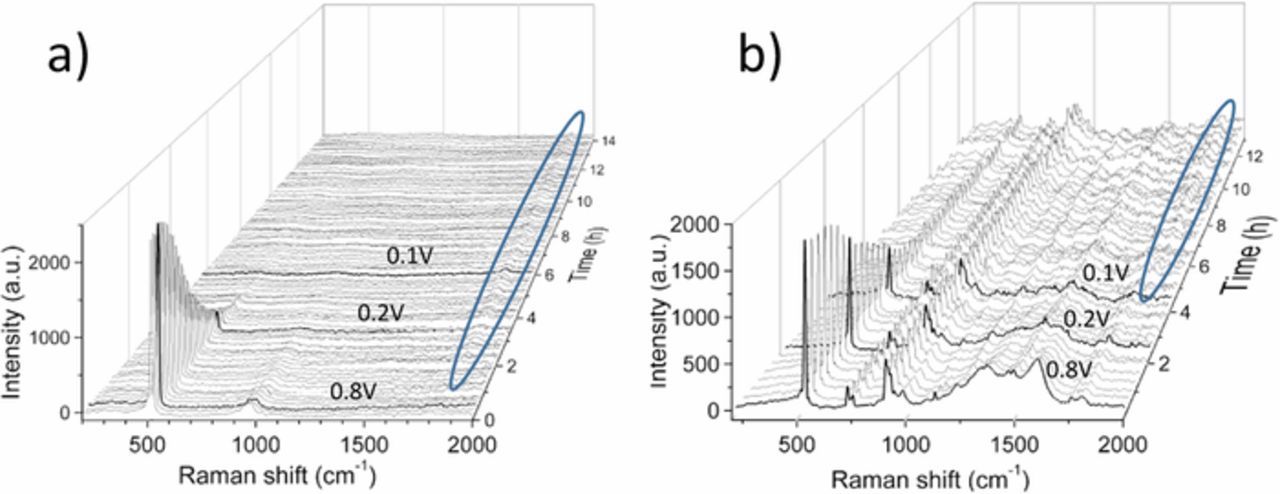
Figure 4. Waterfall charts of the Raman spectra during the first lithiation cycle of uncoated and coated SiNWs. a) Uncoated SiNWs: The initial measurement shows the 1TO and 2TO mode of Si. During lithiation, a strong decrease of the Si 1TO mode is visible at a voltage larger than 0.2V. With the decrease of the Si modes, an increase of an unassigned peak at 1859 cm−1 appears (marked as ellipse). b) Carbon-coated SiNWs: Strong Si and C vibrational modes as well as components of the electrolyte are measured in the initial Raman spectrum. Both Si and C signals decrease with ongoing lithiation. The electrolyte signals remain nearly constant over the whole measurement time.

Figure 6. High intensity Raman measurements of the initial (black), lithiated (red) and delithiated (blue) electrode with a) uncoated SiNWs and b) carbon-coated SiNWs. Spectra for both electrodes are comparable except for the D and G band of carbon and the new feature for uncoated SiNWs at 1859 cm−1.
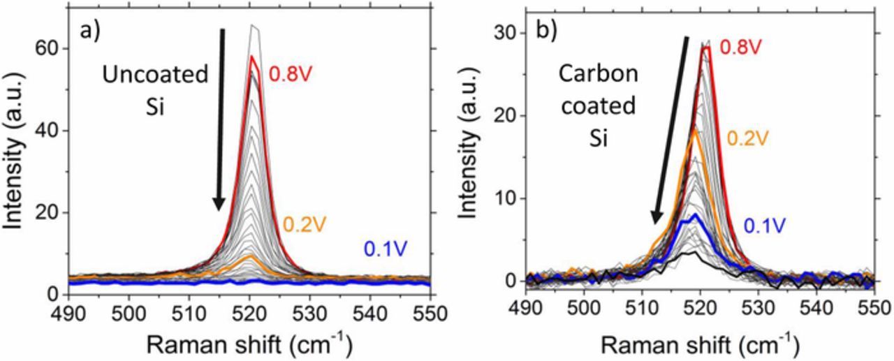
Figure 7. Signal development of the 1TO mode of Si during in situ Raman measurements for a) uncoated and b) carbon-coated SiNWs. The observed intensity drop of uncoated SiNWs occurs above 0.2 V, where Li should not react with Si. In comparison, for the carbon-coated SiNWs the 1TO intensity is distinctly larger at 0.2 V and vanishes with subsequent potential decrease to 0.085 V (black). Between 0.8 V (red) to 0.2 V (orange), a shift of ∼ 2 cm−1 toward smaller wavenumbers occurs. No shift is observed for voltages below 0.2 V.
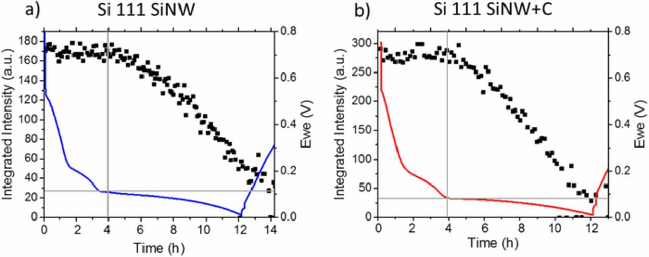
Figure 8. Operando XRD measurement of a Li battery containing a) SiNWs and b) carbon-coated SiNWs as electrodes. The integrated peak intensity of the Si 111 reflection of both samples is shown and compared to the voltage profile of the first lithiation cycle. The Si 111 intensity reduces at a measured potential Ewe of approx. 0.1 V indicating a reaction of Si with Li. The corresponding Si cell parameter changes of both samples are shown in Figure S1, Suppl. Info.
Figure 5 shows the intensity profile as contour plots for the in situ Raman measurements of the uncoated as well as carbon-coated SiNW electrode during the first lithiation and delithiation cycle. In Figure 5a as the Si 1TO and 2TO modes vanish, the new feature at 1859 cm−1 appears simultaneously. It remains constant for the continuing lithiation (red line) and the later delithiation (blue line). No other features are clearly observable. In the delithiation part, distinctly more electrolyte features are visible due to refocusing of the laser spot. They remain constant in the full voltage range up to the final depth of discharge (blue line). A broader signal at approximately 1500 cm−1 is already observed in the fully lithiated state (red line) but gets more pronounced with increasing potential to the complete delithiation state.
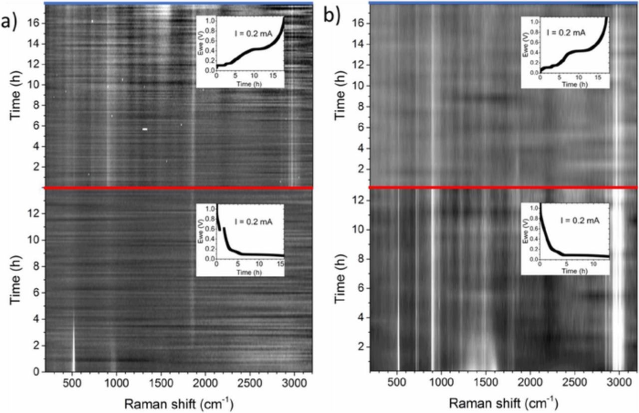
Figure 5. Contour plots of a full lithiation/delithiation cycle of in situ Raman measurements for a) uncoated SiNWs and b) carbon-coated SiNWs. Features which do not change over long time are attributed to the electrolyte. The Si signal diminishes already at high voltages vs Li/Li+. An unknown signal at 1859 cm−1 appears together with the intensity drop of Si. As inset, the voltage profile of the lithiation/delithiation reaction is shown.
Figure 5b shows the comparable development of peak intensities for the carbon-coated SiNWs. The carbon coating can be observed as the typical D and G features. During the lithiation, the carbon signal vanishes earlier at a higher voltage than the Si 1 TO mode, indicating a starting lithiation, as carbon starts to react at a voltage higher than 0.5 V. The typical D and G peaks of carbon are transformed to broadened carbon signal of LiC6 morphology in the lithiated state.35 The carbon coating reduces the maximum intensity of the underlying Si, therefore more features of the electrolyte can be measured. Similar to the uncoated SiNW electrode, a weak signal at 1859 cm−1 arises with diminishing Si signal. It is not as pronounced as the peak observed for the uncoated SiNWs and is only resolved in the low battery potential range.
Detailed high intensity Raman measurements were performed at three stages: before electrochemical cycling, at a voltage of 0.05 V for the lithiated state and at 1.0 V for the delithiated state in the first full cycle. The voltage of both measurements were kept constant during the complete measurement times. The results are shown in Figure 6 for both the uncoated as well as the carbon-coated SiNWs. As shown earlier in Figures 4 and 5, Si, carbon and the electrolyte components are observable. The strong vibrational modes of EC/DMC34,36 in the fingerprint region between 700–1050 cm−1 as well as resulting from the C-H bonds at 2800–3200 cm−1 are visible.36 At 0.05 V in the lithiated and 1.0 V in the delithiated state, the features of the electrolyte remain stable. Interestingly, DMC has a vibrational mode at the Si 1TO position of 520 cm−1, which can only be identified when all the crystalline Si is lithiated and changes to an amorphous state when the intensity of Si modes decreases until becoming almost Raman-invisible. This DMC signal might influence the results of possible Si 1TO mode changes.
As per the reference Raman measurements of several established SEI components recognized by X-ray photoelectron spectroscopy (XPS) in the different charging states,37 broad signals appear between 200–500 cm−1 as well as in the range of 1100–1700 cm−1. Those contributions likely originate from the formation of a stable SEI composed of the above-mentioned reference components. Additionally in the lithiated state of the uncoated SiNW electrode, the feature at 1859 cm−1 is clearly visible, which has not been attributed to a distinct compound of the SEI yet. Strong fluorescence in the battery cell resulted in an increased noise in the Raman spectra, making a high intensity measurement challenging in the desired spectral range, especially in the lithiated state. As a side note, the electrolyte itself turns from transparent in the initial state into milky with subsequent lithiation/delithiation and is attributed to additional fluorescence, making a correct focusing of the laser increasingly difficult.
Figure 7 focuses on the Raman signal of the Si 1TO mode of the uncoated SiNWs and carbon-coated SiNWs during the first lithiation. Possible stress in the crystalline silicon due to lithiation, e.g. as reported by Zeng et al.25 or amorphization of crystalline silicon38,39 should result in a signal shift and/or broadening of the Si 1TO mode. Spectra at certain voltages of 0.8 V, 0.2 V and 0.1 V are labeled in order to highlight the difference between the two samples. For the uncoated SiNW sample, the intensity of the 1TO mode decreased linearly starting at a potential of 0.8 V. In contrast to the literature, no distinct peak shift is observed in the measured voltage range. With the start of lithiation of Si below 0.2 V until vanishing no peak shift can be resolved, therefore it is rather difficult to comment on the stress in SiNWs based on our Raman measurements. The decrease of the Si signal is attributed to the growth of SEI that blocks the Raman signal instead of Si amorphization.
The intensity of the 1TO mode for the carbon-coated Si reduces at a distinctly slower rate. Additionally, a Si peak shift from 520.7 cm−1 to 518.8 cm−1 is observed in the voltage range between 0.8 V to 0.2 V, which is related to a possible lithiation of the carbon coating coinciding with strain toward the underlying Si.40 Again, no signal shift is observed from 0.2 V until the signal is not resolvable from the electrolyte at approximately 0.085 V. The overall decrease of the signal attributed to Si is more likely due to an intensified growth of the SEI that weakens the impinging light intensity on the Si surface by absorbance and in turn reduces the Raman intensity scattered from the sample. Therefore, this behavior may not be associated with an amorphization process.
Interestingly as observed in Figure 4, the signal intensity reduction of the carbon-coated SiNWs is smaller as compared to the uncoated SiNW with decreasing potential, especially in the voltage range between 0.8 V and 0.2 V. The higher intensity at 0.2 V is most likely caused by a weaker reduction of the impinging light due to a thinner SEI.41 The carbon coating might provide besides a more inert surface chemistry a more stable coverage for silicon during lithiation and delithiation buffering the volume changing effects. Without the carbon cover, a notable amount of cracks or new surfaces is formed during repeated cycling often found for silicon anodes.42–44 This reactive surface of uncoated Si results in the increased generation of electrolyte decomposition products leading to a thicker SEI layer followed by a decrease of the Raman signal.
To support the in situ Raman data, similar units of uncoated SiNWs and carbon-coated SiNW electrodes were analyzed using operando XRD especially to better evaluate the Si amorphization during first lithiation cycle. In order to study the structural changes in silicon, the Si 111 reflection was selected and detailed curve fitting and analysis were performed. The integrated intensities of the Si 111 reflection along with the corresponding electrochemistry data was plotted in Figure 8. Initially, the integrated intensities are relatively constant for both materials. An intensity decrease is observed starting at a potential of 0.12 V for the uncoated SiNW and at 0.08 V for the carbon-coated SiNW electrode. The decrease is rather linear, until a minimum intensity is reached. As it has been discussed earlier, silicon does not start to lithiate until a low potential which at least reached 0.2 V. Electrolyte decomposition and SEI formation take place in addition to the lithiation of the underlying carbon fiber substrate as well as the carbon coating on coated SiNWs. Thus, the reduction in reflection intensity of the Si 1TO mode previously shown in Raman measurements at higher potentials than 0.2 V are predominately associated with the reduction of the Raman signal by the reduced amount of impinging light due to the SEI formation on the surface of both the coated and uncoated SiNW instead of amorphization.
Discussion
As shown from the in situ Raman results, the decrease of the Raman signal intensity above a potential of 0.2 V is attributed to the SEI formation accompanied by the increased absorbance of the scattered light. Contrary to literature on Raman measurements, no signal shift is detected normally indicating strain in Si during lithiation of the uncoated SiNWs. Operando XRD measurements show no decrease of integrated intensity at voltages higher than 0.12 V in Figure 8a. The observed drop in Raman signal intensity is mainly traced back to the increased absorbance of the scattered signal by the electrolyte as well as its decomposition products as DMC and EC start to decompose at potentials of approximately 0.8 V.45,46 Nevertheless, as per the operando XRD measurements, a position shift of the Si 111 reflection is observed (Figure S1a, Suppl. Info) at potentials larger than 0.12 V in the range, where no intensity change appears indicating Si lattice relaxation (Figure S1c, Suppl. Info).47
In contrast to the uncoated SiNW, a Raman signal shift is observed between a potential of 0.8 V to 0.2 V of the carbon-coated SiNWs, which was taken as an indication for tensile strain by Zeng et al.40 Operando XRD shows a shift of the Si 111 reflection to lower 2⊖ angles in the same potential range which has been attributed to a lattice relaxation of Si in the Figures S1b and S1d (Suppl. Info) and in literature.47 The strain might be induced by the carbon coating on the SiNW as the lithiation of carbon starts at a higher potential. At a potential below 0.2 V no peak shift is derived from the measurements, while operando XRD visualize a drop of the integrated intensity of the Si 111 reflection related to the beginning of the lithiation (Figure 8b). Nevertheless, it cannot be excluded, that there is a convolution of positive and negative influences by additional aspects e.g. high conductivity due to carbon coating vs. strain related inhibition of lithiation leading to alternative outcomes and may require further study.
In addition to the Si and C signals, the electrolyte shows distinct features at various positions, which are directly attributed to EC and DMC in LiPF6 as reported in literature (overview in Table I). This behavior is also indicated by a permanent presence of the signal independent of the battery potential. A novel feature is found during the lithiation especially for the uncoated SiNW electrode. A singular signal at ∼1859 cm−1 occurs coinciding with a vanishing Si signal. So far, no Raman measurement of SEI species have been presented in literature which allows to assign this signal to a specific compound. From XPS results in literature, an SEI layer composition is derived which consists of hydrocarbons, polyethylene oxide (PEO)-type oligomers, LixPFy, LiF, and LixPFyOz products (0.5 V), hydrocarbons and PEO-oligomers (0.1 V), Li2CO3 and LiF (0.01 V), respectively, with Li2CO3 as a major constituent.48,49 EC-containing solutions contain contributions from Li2CO3 and ROCO2Li species (resulting from EC and DMC reduction).41,48 Other than those, such as Li carbonates and fluorides already known as SEI components on graphite, significant amounts of Si electrode-unique SEI species were detected.50 On an uncoated Si electrode, high concentrations of C and Si fluorides, like SiOxFy, appear after long cycling. Characteristic for the constitution of the SEI of carbon-coated silicon nanoparticles cycled vs. Li/Li+ was the absence of Si and C fluorides but the presence of siloxane species.50 Table I summarizes possible components of the SEI from XPS and Raman measurements. Compared to literature on electrolyte components and electrode materials, we suggest that this contribution may originate from signals of carboxylic anhydrides or diacyl peroxide compounds. Alternatively, phosphines with P-H bonds from the conductive salt are possible after distinct shift to lower wavenumbers. Nevertheless, no clear data has been found for the observed signal, therefore this SEI component remains unassigned.
Table I. Different battery constituent species and possible SEI components as observed in the Raman measurements in correlation with literature.
| SEI component | Raman signals | Ref |
|---|---|---|
| c-Si peaks | 2TA: 306 cm−1 | 51 |
| 1TO: 520 cm−1 | ||
| TO+TA: 618 cm−1 | ||
| 2TO: 963 cm−1 | ||
| Electrolyte | 510 cm−1 | 34,36 |
| LP30 electrolyte | 739 (two) cm−1 | |
| 900 (two) cm−1 | ||
| 2800–3200 cm−1 (multiple) | ||
| Li2CO3 | 95, 123, 156, 192, 711, 748, 1091, 1459 cm−1 | 52,53 |
| LiF | 210, 263, 384, 417, 435, 508 cm−1 | 54 |
| Li2O, LixSiOy (Li4SiO4): formed by reaction with surface SiO2 layer | Li2O Raman signal: 523 cm−1 | 55,56 |
| Carbon fluorides: | 57 | |
| ○ graphite powder two Raman modes at 1580 (E2g2) and 1360 (A1g) | ○ 1583–1593 cm−1 | |
| ○ Mode at 1580 splits into two modes after fluorination | ○ 1542–1555 cm−1 | |
| ○ Mode D shifted for fluorinated graphite | ○ 1360 cm−1 shifted to 1356−1337 cm−1 in fluorinated state | |
| LiOH: | • 287, 299, 329 (strong), 519, | 58 |
| ○ present after lithiation (10 mV) | 620, 3663 (very strong) cm−1 |
The in situ Raman results demonstrate the advantage compared to operando XRD toward revealing the changes in amorphous as well as liquid components and is a very helpful and necessary complementary tool to support the results of morphology changes typically observed by XRD. In situ Raman spectroscopy may be also more sensitive to transient species than XPS in this case. XPS as a high vacuum technique can change the surface composition and may not give suitable results at a certain SEI thickness, as only the SEI is detected. This hindrance is often eliminated with a washing and sonication step in literature. The in situ analysis also reveals a previously unknown signal of SEI formation for uncoated Si at 1859 cm−1, likely an SEI component which has not been observed for the carbon-coated SiNW. As this signal increase correlates well with the intensity reduction of the signal attributed to Si, this reaction might be caused by the uncoated Si surface exclusively. The carbon coated SiNWs do not expose much Si to the electrolyte, therefore the overall amount of this component is lower.
Conclusions
We have successfully shown in situ Raman spectroscopy measurements on a silicon nanowire anode material and compared the results to the same structure with carbon-coated silicon nanowires. We used an advantageous setup of a three dimensional substrate uniformly covered with silicon nanowires in three dimensions. This electrode design allows a unique spectro-chemical observation of a battery cell keeping the modification to the structure to a minimum. We observed differences in the decrease of the Si 1TO mode for the uncoated SiNWs versus the carbon-coated SiNWs. Strong electrolyte signals are visible during the full cycle. A so far unassigned peak appears at 1859 cm−1 with the decrease of the Si signal for both samples and can be correlated to a currently unknown SEI species on the surface of the nanowires. The presented results are further supported by operando XRD measurements of similar samples which helped us to identify differences caused by structural changes in the silicon nanowires themselves.
Acknowledgments
We gratefully thank Anne Baasner (Fraunhofer IWS) for providing various chemicals as well as Tony Jaumann (IFW Dresden) for support with the synchrotron XRD measurements. Beamtime allocation at the BL04-MSPD beamline at the ALBA Synchrotron in Barcelona, Spain, is gratefully acknowledged. We also highly appreciate the financial support by the German Federal Ministry of Education and Research (BMBF) through the Excellent Battery – WING center "Batteries - Mobility in Saxony" (grant no. 03X4637).
ORCID
Andreas Krause 0000-0002-2866-8462