

Abstract
Device degradation due to hot carrier injection (HCI) in multi-fin 20 nm and 10 nm N- and P-type FinFET devices are thoroughly analyzed. To further understand the HCI reliability of the four FinFET devices, the device is fabricated with a standard Vt base and low Vt base gate stacks with different work functions. It is evident that: (i) The standard Vt device sustains lower effective stress bias due to the difference in threshold voltage, resulting in a more stable threshold voltage than the low Vt base device, and (ii) the transconductance of the single N- and P-type FinFET is more severely degraded than the multi-fin N- and P-type FinFET, mainly because multi N- and P-type Finfet has coupe effect, which effectively reduces the impact of HCI.
Export citation and abstract BibTeX RIS
Technological development in the semiconductor industry and the feature size of transistors have followed Moore's law for constant scaling of the device. Increasing the operating speed to reduce manufacturing costs, enhancing device performances, engineering various threshold voltages (Vt) to lower power consumption, and fabricating high-speed devices are performed by different researchers. 1–3 To achieve the speed and power of the device, the device scaling moves from submicron to deep submicron. Starting towards the three-dimensional structure (3D) development, among all transistors, the fin-type developed by ChengMing Hu's team field effect transistor (FinFET) is the promising transistor architecture at the moment. 4–6 The primary challenge device faces at the deep submicron level is short channel effects (SCE). Effects cause drain-induced barrier lowering (DIBL), current collapse (breakdown), the penetration phenomenon (punch-through), gate leakage current, and quantum tunneling occurs, which will affect the electrical characteristics of devices and limit further development. 7–9 Multigate FET structures can reduce the short channel effect as it controls the channel from many directions. Therefore, researchers exploited the available space in device structure techniques and their physics to enhance performances. 10,11 Doping concentration variation in source/drain is the other technique, but the leakage becomes inevitable because of direct tunneling. 12 Thus, a high-k dielectric layer (HfO2) with a metal gate is introduced to replace the silicon dioxide (SiO2). 13 Hafnium oxide (HfO2) high-k dielectric material needs to be stacked with the effective work function (EWF) metal gate. Introducing the intermediate energy level (Mid-Gap) metals such as titanium nitride (TiN, pWFM) or aluminum tantalum (TiAl, nWFM) which modulates the work function of the metal gate. 14–16 This material suppresses the gate leakage current while improving the device's characteristics. However, high dielectric constant materials and metal gates are also accompanied by higher interface density, charge trapping (interface/oxide trapped charge (Qit, Qot), Mobile ion charge (Qm) and fixed charge (Qf), charge trapping/de-trapping, low drift rate (low mobility) and other disadvantages. 13,17,18 The HCI also degrades the device's reliability through physical deformation or defects. 19
Hot carrier effect is a phenomenon that causes carriers to deorbit when the drain terminal is subjected to a transverse electric field (EDS = (VDS/Lg) effect, gaining energy and deviating from the intended path, generating numerous electron-hole pairs at once and subsequently affecting itself, colliding and dissociating (impact ionization). 20,21 Some of these electron-hole pairs will be affected by gate terminal voltage. In contrast, others tunnel into the gate oxide layer (interface, SiO2, high-k), and it becomes trapped charges or fixed charges or break bonds at the oxide/silicon interface (Si–H), forming an interface state. 22 Some of these EHP will move into the substrate and constitute the substrate current, resulting in device performance degradation in switching characteristics of the fin field effect transistor. Hot carrier effects are often the cause of device and circuit failure. In this paper, as traps stem from HCI, the effect of HCI on the performance for HCI stress time from 0 s to 3000 s was investigated for reliability. 23–26 This paper will study the fabricated three-dimensional structure of the fin field effect transistor for multiple fin structures, P-type work function metal TiN thickness (pWFM) named as low Vt Device and N-type work function metal TiAl thickness (nWFM) named as standard Vt device, the difference in the thickness of the material on the gate stack to change Vt, in line with the needs of single to multi-FinFET design. The multi-FinFET device with a standard Vt base and low Vt base was used to measure the device's electrical characteristics. Furthermore, the effect of HCI on the performance for different stress times HCI stress time from 0 s to 3000 s was investigated for reliability. The detailed reliability analysis of the device is the main finding of this research work. The high voltage stress of 1.25 V and 1.45 V applied to the gate and drain for N-type devices and −1.25 V and −1.45 V for P-type devices can be utilized in various circuits to assess the reliability, performance characteristics, optimize the operating range and stability of the circuits.
Experiment
Figure 1a shows the device schematic fabricated in this work, while Fig. 1b shows the detailed gate stack layers of the devices, namely, N-type low Vt FinFET device, N-type standard Vt FinFET device, P-type low Vt FinFET device, P-type standard Vt FinFET device. MOCVD is used to grow the channel over the substrate.
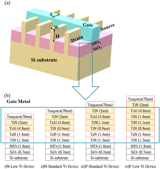
Figure 1. (a) Schematic of Fabricated Multi-FinFET, (b)The stack of Low Vt and Standard Vt N- and P-type FinFET.
Download figure:
Standard image High-resolution imageSpacer lithography and dry, wet etching are used to create the Fin design. The defined etching technique well regulates in fabricating Fin's dimension. The Transmission Electron Microscope (TEM) image of the fin is evident that the multi-Fin is properly formed and not flatulated, which is shown in Fig. 2. To accelerate carrier transport through the channel region, a high tensile stressor SiN is incorporated as the contact etch stop layer (CESL). The gate metal stacks of the N- and P-type standard Vt FinFET devices consist of an additional TiN layer than the N- and P-type low Vt FinFET devices.
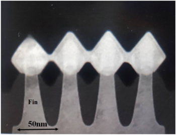
Figure 2. Transmission Electron Microscope (TEM) image of multi-Fin in fabricated FinFET device before gate metal deposition.
Download figure:
Standard image High-resolution imageFigure 3 shows an energy diagram of an unbiased MOSFET with multi-threshold voltage (Vt) resulting from a difference in the gate's work function. It is desirable for the WFM in n-channel and p-channel MOSFETs to have a low work function, around 4.1 and 5.1 electron volts (eV) respectively. The additional TiN layer is mainly due to the work function engineering. When a positive voltage is supplied to the gate electrode, band bending occurs and confines electrons at the oxide/semiconductor junction. As a result, the standard device exhibits more reverse mode behavior, leading to a higher Vth due to its higher inversion level or work function. In addition, compared to the N-doped FinFET devices, the P-doped FinFET devices feature two more TiN layers, also owing to the work function engineering of different dopants.
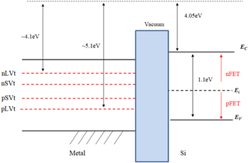
Figure 3. Energy diagram of unbiased N- and P-type FETs that use a WFM gate to adjust the threshold voltages.
Download figure:
Standard image High-resolution imageResults and Discussion
The electrical characteristics of single- and multi-FinFET devices are measured using a semiconductor parameter analyzer (Agilent-B1500A). To accelerate the degradation due to HCI and to better understand the electrical characteristics under harsh conditions, high voltage stress of 1.25 V and 1.45 V was applied to the gate and drain for N-type devices, high voltage stress of −1.25 V and −1.45 V was applied to the gate and drain for P-type devices, for a period ranging from 0 to 3000 s.
The N-type FinFET hot carrier injection reliability
N-type low and standard Vt FinFET's ID-VG characteristics are depicted in Fig. 4. At the same time, Fig. 4a shows the ID-VG characteristics of the N-type low and standard Vt FinFET device with single fin, and Fig. 4b shows the ID-VG characteristics of the N-type low and standard Vt FinFET device with four fins. In Fig. 4a, The Vth variation percentages under a stress time of 3000 s were 40.69% and 20.3% for low Vt and standard Vt single fin FinFET devices, respectively. Due to the difference in threshold voltage, the stress voltage on the gate, even though it is the same condition, the bias creates a difference in effective stress bias, as Fig. 5 shows. Thus, despite showing lower operating bias and better transconductance, the low Vt FinFET device has demonstrated worse reliability characteristics. In result of withstanding a larger effective stress bias than the standard Vt FinFET device.
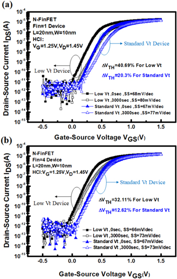
Figure 4. Transfer characteristics of Low and Standard Vt for N-type FinFET. (a) Fin = 1, and (b) Fin = 4.
Download figure:
Standard image High-resolution image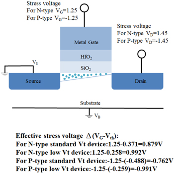
Figure 5. An schematic illustration of effective stress on oxide.
Download figure:
Standard image High-resolution imageIn Fig. 4b, the Vth variation percentages under stress time of 3000 s were 32.11% and 12.62% for low Vt and standard Vt four-fin FinFET devices, respectively. From Figs. 4a and 4b, regardless of the fin number, the trend is the same; the degradation of the low Vt devices is more severe than that of the standard Vt devices. The single-fin and four-fin low Vt FinFET devices show a 20% increase in Vth degradation. However, it has been observed that four-fin FinFET devices show overall less Vth degradation due to the coupe effect of multi-fin FinFETs.
Figure 6 shows the Gm-VG of the N low and standard Vt FinFET devices with fin numbers one and four. The transconductance degradation percentages under a stress time of 3000 s were 21.6% and 11%, for low Vt and standard Vt single-fin FinFET devices, 8.9%, and 8.2%, for low Vt and standard Vt four-fin FinFET devices, respectively. The low Vt FinFET devices exhibit better transconductance. However, before and after the HCI test, the transconductance characteristics behave similarly to the Vth variations, in which low Vt FinFET devices show more severe transconductance degradation than the N standard Vt device.

Figure 6. (a) Low and Standard Vt Transconductance for Fin = 1 N-type FinFET. (b) The transconductance of Low and Standard Vt for Fin = 4 N-type FinFET.
Download figure:
Standard image High-resolution imageFigure 7 demonstrates a charge density model, an explanation of the mechanism of the HCI reliability improvement of the four-fin FinFET device. As the distance between fins decreases and fin number increases, such as in the case of the four-fin FinFET device, due to the interaction between the electrons in the fins, the density of electrons will decrease. This is the so-called "coupling effect" between neighboring fins. As a result of the coupling effect between adjacent fins in multi-fin structures, the inversion charge density in the fin channel reduces, lowering the drain current per fin (normalized ID) and affecting ionization during HCI stress. For multi-fin FinFETs, HCI reliability enhances with increasing fin numbers. The coupe effect of the four-fin FinFET device during the HCI test (Fig. 4b) could effectively reduce the impact of hot carrier injection by mitigating the ionization caused by the high voltage bias applied to the device during the HCI test. 20,21 Low Vt and standard Vt four-fin FinFET devices displayed an 8% decrease in Vth degradation than those with single fin.

Figure 7. Coupling Effect for Single and Multi FinFET.
Download figure:
Standard image High-resolution imageThe P-type FinFET hot carrier injection reliability
To comprehensively analyze the HCI effects on FinFET variation, P-type FinFETs are also measured and discussed in this section. Due to the different operations, one being positively switched and one being negatively switched, analyzing both N-type and P-type could benefit understanding fin variations on the impact of HCI reliability issues. Figure 8 shows the ID-VG characteristics of the low and standard Vt pFinFET devices with different fin variations (single and four). In Fig. 8a, The Vth variation percentages under a stress time of 3000 s were 25.54% and 12.71% for low Vt and standard Vt single-fin FinFET devices, respectively. The result of the minor Vth degradation in the P standard Vt device is the same main reason as the N standard Vt device; a lower effective stress bias was applied to the gate. In Fig. 8b, the Vth variation percentages under stress time of 3000 s were 18.1% and 7.13% for low Vt and standard Vt four-fin FinFET devices, respectively. Four fin standard Vt FinFET devices displayed consistent N- and P-type results, showing the least Vth degradation. Multi FinFET, with the help of the coupling effect, demonstrates inhibition on the HCI reliability issues.
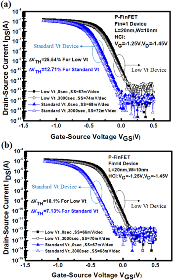
Figure 8. Transfer characteristics of Low and Standard Vt for P-type FinFET. (a) Fin = 1, and (b) Fin = 4.
Download figure:
Standard image High-resolution imageFigures 9 and 10 are combined graphs of the Vth variation of single-fin and four–fin N- and P-type FinFET devices. The charts pinpoint the Vth degradation at each time interval. P-type FinFETs show less Vth degradation due to the additional TiN layer, both low Vt and standard Vt devices.
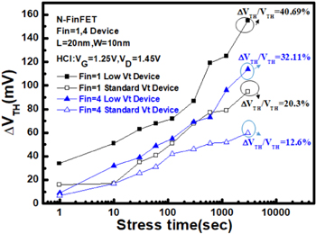
Figure 9. Low and Standard Vt shift concerning stress time in N-type FinFET in the different stress time domains.
Download figure:
Standard image High-resolution image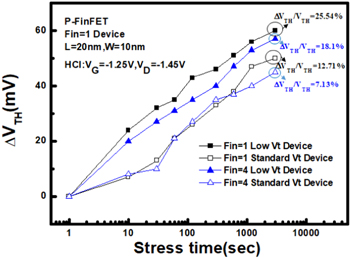
Figure 10. Low and Standard Vt shift concerning stress time in P-type FinFET in the different stress time domains.
Download figure:
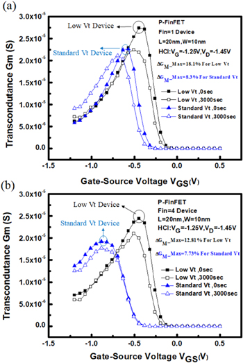
Standard image High-resolution imageFigure 11 shows the Gm-VG of the N low and standard Vt FinFET devices with fin numbers single and four. The transconductance degradation percentages under a stress time of 3000 s were 18.1% and 8.3%, for low Vt and standard Vt single-fin FinFET devices, 12.81%, and 7.73%, for low Vt and standard Vt four-fin FinFET devices, respectively. Table I shows the list of the complete comparison of the Vth degradation and transconductance degradation after the HCI test. The four-fin P-type standard Vt FinFET device shows minor transconductance degradation (7.73%), lower than the four-fin N-type standard Vt FinFET device (8.2%). N-type standard Vt FinFET device, doped with As, could potentially create AlAs alloy, causing further lattice mismatch and the generation of external deep traps. The more considerable transconductance degradation of the N-type standard Vt FinFET device could prove the existence of more trapping sites.
Figure 11. Transconductance of Low and Standard Vt for P-type FinFET. (a) Fin = 1, and (b) Fin = 4 Device.
Download figure:
Standard image High-resolution image
Table I. Impact of Fin number variation (Fin = 1 and Fin = 4) on HCI-induced performance degradation.
| Variation in Fin number | Device | Initial transconductance | Initial threshold voltage |
|---|---|---|---|
| Fin = 1 | P-type Standard Vt Device | 0.027 mS | −0.488 V |
| N-type Standard Vt Device | 0.026 mS | 0.371 V | |
| P-type Low Vt Device | 0.023 mS | −0.259 V | |
| N-type Low Vt Device | 0.028 mS | 0.258 V | |
| Fin = 4 | P-type Standard Vt Device | 0.076 mS | −0.431 V |
| N-type Standard Vt Device | 0.101 mS | 0.360 V | |
| P-type Low Vt Device | 0.096 mS | −0.249 V | |
| N-type Low Vt Device | 0.107 mS | 0.241 V | |
| Variation in Fin number | Device | Variation in transconductance degradation | Variation in threshold voltage degradation |
| Fin = 1 | P-type Standard Vt Device | 8.3% | 12.71% |
| N-type Standard Vt Device | 11% | 20.3% | |
| P-type Low Vt Device | 18.1% | 25.54% | |
| N-type Low Vt Device | 21.6% | 40.69% | |
| Fin = 4 | P-type Standard Vt Device | 7.73% | 7.13% |
| N-type Standard Vt Device | 12.81% | 18.1% | |
| P-type Low Vt Device | 8.2% | 12.62% | |
| N-type Low Vt Device | 8.9% | 32.11% |
Conclusions
This research paper discusses two main research aspects, the variation of the number of fins from 1 to 4 and the thickness of the TiN regarding work function engineering as standard Vt and low Vt N- and P-type FinFET. High voltage stress is applied to the gate and drain terminals to understand hot carrier injection reliability issues. HCI stress time substantially impact the subthreshold region of drain current in both low Vt and standard devices. The fin field effect transistor's electrical characteristic analysis and reliability research with the metal gate structure is also analyzed. In the multi-gate, the reduced equivalent fin height coupled with the coupling effect of multiple fin structures results in a drop in the equivalent electric field. Due to this phenomenon, the electrical characteristic analysis threshold voltage shift (ΔVt), transconductance (gm) of multi-FinFET shows good performance compared to single fin channel structure, both N- and P-type FinFETs. From the good reliability result, the multi-fin channel standard FinFET device is a suitable structure since it is more resistant to the HCI effect.
Acknowledgments
This work was supported by the Ministry of Science and Technology Taiwan under Contract MOST 108–2923-E-492-002 -MY3 and 108–2221-E-492-029 -MY3, and the authors would like to thank the staff of Taiwan Semiconductor Research Institute (TSRI) for their commendable support. Availability of Data and Materials. All device data are included in this manuscript. Declaration of competing interests. The authors declare no competing financial interests or personal relationships that could have appeared to influence the research work reported in this paper. Authors' contributions. First Author has carried out the Research work. All other authors have an equal contribution to supporting the research work.