
Abstract
This study presents a stacked process of thermal and atomic layer deposition (ALD) SiO2 that reduces the interface trap density of 4H-SiC metal-oxide-semiconductor (MOS) capacitors. The channel mobility of metal-oxide-semiconductor field effect transistors (MOSFETS) are reduced due to the high interface trap density as well as coulomb scattering mechanism. Herein, we investigate SiO2/SiC interface properties of a stacked process, which is accomplished via reducing the thickness of thermal oxidation film. Notably, MOS capacitors fabricated with thermal and ALD SiO2 stacked structures can reduce the interface states density (Dit) by twofold at 0.2 eV below the conduction band energy compared with thermally grown SiO2. Additionally, the leakage current increases at a relatively slow rate in the electric field of 5–10 MV cm−1, whereas the leakage current increases sharply when the electric field is higher than 10 MV cm−1. The resultant ALD SiO2 stacked structure provides a new approach to improving interface quality, which allows a reduction in the thermal budget involved in the fabrication of devices.
Export citation and abstract BibTeX RIS

This is an open access article distributed under the terms of the Creative Commons Attribution Non-Commercial No Derivatives 4.0 License (CC BY-NC-ND, http://creativecommons.org/licenses/by-nc-nd/4.0/), which permits non-commercial reuse, distribution, and reproduction in any medium, provided the original work is not changed in any way and is properly cited. For permission for commercial reuse, please email: permissions@ioppublishing.org.
4H-SiC has received considerable attention owing to its high thermal conductivity, high carriers saturation drift rate, and high breakdown electric field. Moreover, power devices made of SiC materials are commonly used in the field of power electronics. The primary cause of restricted performance in 4H-SiC MOSFET power devices is high on-resistance, which decreases device mobility and, consequently, device performance. Moreover, the interface defects between SiO2 and SiC trap carriers and reduce the number of carriers during device conduction. Therefore, the device performance should be enhanced by improving the interface quality. 1 Meanwhile, the coulomb scattering mechanism of carriers near the interface can also decrease mobility. One study reported that the inversion layer carrier mobility of 4H-SiC is significantly lower than its bulk mobility. 2 The low mobility of channel has long been the subject of extensive studies. These studies have often linked the low mobility to investigations on the SiO2/Si interface of Si devices. 3,4 At the same time, high Dit exists at the interface between SiC and thermally grown SiO2, consisting of Si dangling bonds, C dangling bonds, or "C-C" bonds at the interface. 5 In addition, defects in the oxide layer near the interface and some substrate defects had also been considered major contributions to low channel mobility. 6,7 NO annealing after oxidation is the most established process for forming high quality oxidation film with low interface traps on 4H-SiC and N elements can passivate the SiO2/SiC interface and decomposed carbon clusters. 8 Other process gases, such as a mixture of two gases 9 or P-element gases, had also been employed to passivate the SiO2/SiC interface. However, passivating the interface with P-element can result in a significant threshold voltage drift. 10 Some studies had also adopted methods involving element doping or chemical vapor deposition process to improve interface quality. 11–13 In summary, high temperature thermal oxidation process is the most established technology for forming SiC MOSFET gate dielectric. The thickness of dielectric film in the actual MOSFET device is around 50 nm, and this requires a longer oxidation time. At the same time, the growth rate has also decreased and there are more defects in the interface. The atomic layer deposition (ALD) process is extensively used for its precise control of film thickness and roughness. Methods of growing high dielectric constant insulation layers or combining thermal oxidation film with ALD has been widely discussed in previous studies, which can reduce interface defects; 14–16 however, high dielectric constant films produce more defects within the oxidation layer. Therefore, we propose a new structure that can reduce interface defects and close to the needs of actual device. In this study, a new stacked structure of both thermal and ALD SiO2 is proposed to improve interface quality. The gate dielectric film is formed by thermal oxidation process and ALD deposition process. Further, the interface characteristics and leakage characteristics of the prepared MOS capacitors are analyzed in detail.
Experimental
We fabricated MOS capacitors to study SiO2/4H-SiC interface properties. Samples used in the experiments were commercially available n-type epitaxial 4° off-axis oriented 〈11–20〉 SiC wafers with Si-plane (0001) orientation, an epitaxial layer thickness of 10 um, and a doping concentration of 8 e15 cm−3. First, the samples were cleaned using the Radio Corporation of America process. Then, the sacrificial oxide layer was grown and rinsed off with 10% HF to remove contaminants and the nature oxide layer while simultaneously reducing the surface roughness of the wafers. Second, some samples were oxidized in an O2 atmosphere at 1400 °C for 2 min, followed by a NO annealing process at 1200 °C for 70 min. After thermal oxidation, the sample underwent NO annealing and underwent reoxidation phenomenon, so the thickness of thermal SiO2 was thick. The average thickness of SiO2 was measured to be 15 nm using ellipsometry, followed by ALD SiO2 deposition process, resulting in a final total SiO2 thickness of 48 nm, the temperature of the ALD process was 300 °C, the precursor used was ozone and di-isopropylaminosilane (DIPAS, C6H17NSi), with N2 gas used as a carrier gas. The remaining samples underwent a process of dry oxygen oxidation at 1400 °C for 13 min and annealed at 1200 °C for 70 min; SiO2 thickness was measured to be approximately 55 nm. Both samples underwent NO annealing process. Third, aluminum electrodes and backside electrodes were grown using a sputtering process. The measurement pattern was made through photolithographic process with an electrode thickness of 1 μm, the area of metal electrode was 2.54 × 10⁻⁴ cm2, all electrical characteristics were obtained using Keysight B1505 measurement analyzer, and we measured capacitance-voltage (C–V) and current-voltage (I-V) electrical characteristics.
Results and Discussion
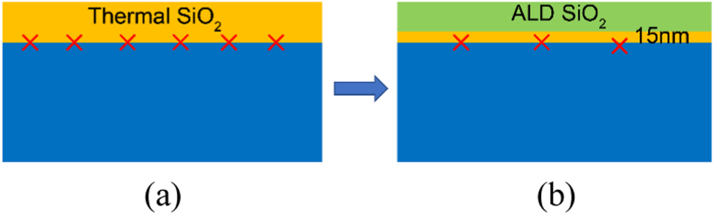
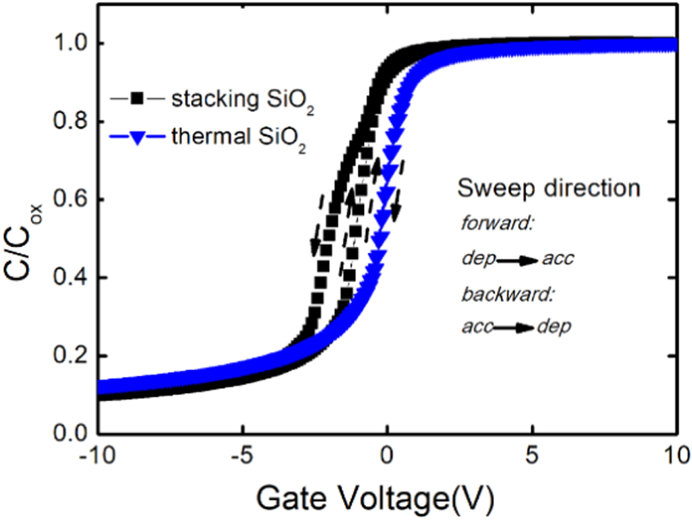
The schematics of the stacked and thermal SiO2 structures are shown in Fig. 1. There are no voids between the ALD stacking SiO2 and thermal SiO2. Owing to the high oxidation temperature, excessively short oxidation times can result in uneven distribution of oxygen gas in the reaction chamber, resulting in poor uniformity of oxidation film; therefore, a 2 min oxidation condition is reasonable, with the final oxidation film thickness being approximately 15 nm. The oxidation rate of thermal SiO2 gradually decreases with the increase of oxide film thickness. For a thin thermal oxidation layer, the oxidation reaction rate is higher, which can effectively reduce the interface defects between SiO2 and SiC. Oxygen gas in the reaction chamber should be uniformly distributed, and the oxidation time should be as short as possible, and the thickness of the thermal oxidation film should be as thin as possible. Moreover, the thickness of SiO2 is strongly correlated with the interface states density. 17 Therefore, when the thermal SiO2 film is relatively thin, the oxidation reaction rate can be increased to reduce interface defects. The high-frequency C–V curves of the two MOS capacitor samples are shown in Fig. 2. The theoretical curves of the MOS capacitors are also added for comparison, and the C–V characteristics were obtained at 1 MHz with a voltage sweep step of 0.1 V in the scanning from −10 V (deep depletion region) to 10 V (the accumulation region). Figure 2 shows that the flatband voltage of the stacked structure tends to drift slightly to the left compared with the theoretical curve, indicating that positive charges are trapped by the donor-like oxide film defects, resulting in the hole injection phenomenon. In contrast to high temperature thermal oxidation reaction, ALD has a low process temperature. Further, silicon and oxygen elements generated by the decomposition of precursor are adsorbed onto the thermal oxidation film, which reacts to generate silicon oxide. Simultaneously, the products of precursor decomposition also generate hydroxide radical. At the same time, under similar ALD process conditions with the same precursor, oxygen vacancies have been detected via X-ray photoelectron spectroscopy. 18,19 Herein, oxygen vacancies exhibit donor like traps, capturing positive charges. Consequently, the flatband voltage of a stacked structure is more negative than that of thermal oxidation structure. The C–V frequency dispersion characteristics of the thermal SiO2 structure and ALD stacked structure at the measurement frequencies of 1, 10, 100, and 1 MHz are shown in Figs. 3a and 3b. Figure 3 shows that the frequency dispersion characteristics of the stacked structure are not significantly different from that of the thermal SiO2 structure, indicating that the interface quality of the stacked structure has not been compromised. Meanwhile, a bulging phenomenon, which is the result for appearance of deep energy level traps in the oxide film, was observed. According to the relationship between surface potential and SiC energy level, the bulge was approximately 1–2 eV below the SiC conduction band energy. However, no bulging was observed in the C–V curve of thermal oxidation structure. We believe that bulging is caused by oxygen vacancy defects in the ALD film, oxygen vacancy defects capture hole carriers and causing abnormal changes in the multi frequency C–V curve. The essence of bulging phenomenon has also been mentioned in other studies. 20 The following section presents a further discussion on oxidation film defects. Figure 4 shows the C–V hysteresis characteristics curves of two structures, the C–V curves scans from the negative voltage depletion state to the positive voltage accumulation state and vice-versa. The C–V characteristic of the stacked structure shifted significantly to the left during the reverse scanning process, whereas the C–V characteristic of the thermal oxidation film shifted slightly to the right. This also proves that the defect type of the two oxidation films were different.

Figure 1. (a) Schematic of thermal SiO2 structure and 1(b) Schematic of ALD process stacked structure.
Download figure:
Standard image High-resolution image
Figure 2. C–V curve of MOS capacitor with thermal SiO2 and stacked SiO2 structure at 1 MHz frequency.
Download figure:
Standard image High-resolution image
Figure 3. (a) C–V dispersion characteristics of thermal SiO2 structure. (b) C–V frequency dispersion characteristics of stacked structure.
Download figure:
Standard image High-resolution image
Figure 4. C–V hysteresis characteristic curves of two types of capacitor structures.
Download figure:
Standard image High-resolution imageThe distribution of the interface states density along the conduction band energy level extracted using a high-frequency and quasi-static method is shown in Fig. 5. Quasi-static C–V characteristic measurement involves the application of a very slow (<0.1 V S−1) time-varying voltage signal linearly increasing over time to the gate electrode, simultaneously using a sensitive ammeter to measure the current flowing through the MOS capacitor. Based on the amplitude of changes in gate current and gate voltage, the quasi-static capacitance can be obtained, which is calculated using Eq. 1.

Figure 5. Distribution of interface states density along the energy level for MOS capacitors with stacked structures and thermal SiO2 structures.
Download figure:
Standard image High-resolution imageHerein, the interface states density of the stacked structure is further reduced compared with the thermal SiO2 structure at 0.2 eV below the conduction band energy level. In contrast to the thermal SiO2 structure, the stacked structure can reduce the interface states density by two times. Moreover, a steeper decreasing trend of Dit along the energy level is observed, which is consistent with the theory that reducing SiO2 film thickness can increase the thermal oxidation rate. Therefore, this approach can be considered for device fabrication to reduce the thermal budget while reducing interface defects. This stacked structure provides a new method for replacing the thermally oxidized gate dielectric film of SiC MOSFET and may improve power device performance.
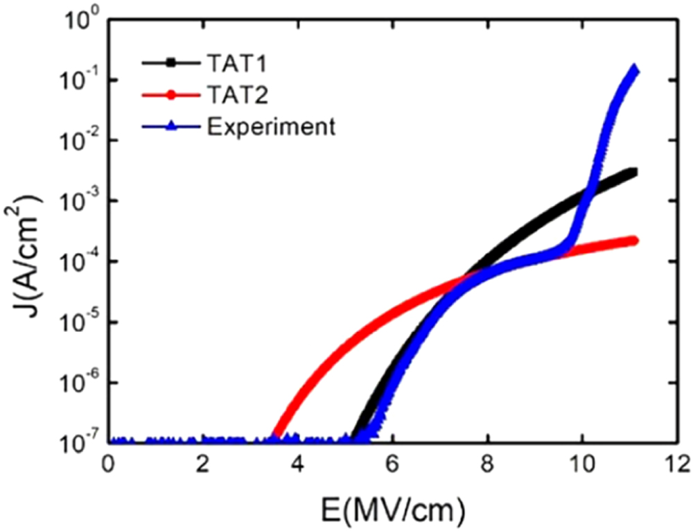
The leakage characteristics of the two samples were also analyzed by continuously applying a gradually increasing gate voltage to the samples until their breakdown. Moreover, the relationship between the current density and electric field is shown in Fig. 6.

Figure 6. Leakage current-electric field characteristic curve of stacked structure and thermal SiO2 structure.
Download figure:
Standard image High-resolution imageThe electric field is obtained using Eq. 2:

where  is the gate voltage,
  is the flatband voltage, and
  is the thickness of the oxide film. The Fowler–Nordheim current is defined using Eq. 3, where
  is the gate area, and
  is the gate electric field. A and B are the coefficients, obtained using Eqs. 4 and 5.


Figure 6 shows the I–V curves of the stacked SiO2 structure and thermal oxidized sample measured at room temperature 25 °C. For thermal oxidized sample, electrons would accumulate at the SiO2/4H-SiC interface because of a positive bias. Moreover, electrons cross barrier height through Fowler–Nordheim tunneling. The barrier height of SiO2/SiC obtained through the F–N current formula is 3.05 eV. For stacking SiO2 sample, a faster increase in current can be observed starting from 5 MV cm−1, the oxidation film grown by ALD produced different types of defects, which results in a differently shaped I-V curve compared to the thermal oxidation structure I-V curve. We used model parameter fitting methods to determine the current conduction mechanism in different electric field. The leakage current in the low electric field range included trap assisted tunneling (TAT),
21,22
hopping conduction.
23,24
Fowler Nordheim (F–N) tunneling, and Poole Frenkel (P–F) effect, which are the leakage mechanisms observed in the high electric field range.
25,26
We confirmed that in the low electric field range, TAT and hopping conduction were the current conduction mechanisms, whereas in the high electric field range, the hopping conduction and P–F emission were dominant. The specific current fitting process can be found in the literature.
27
Table I, Table II and Table III list the fitted parameters, where  is the trap energy level relative to the oxidation film conduction band, a is hopping distance, Ea is activation energy, and R2 is a fitting linear correlation parameter.
Table I. TAT fitting parameters.
| Electric field |

| R2 |
|---|---|---|
| (MV cm−1) | (eV) | |
| 6–7.5 | 1.67 | 0.99948 |
| 7.5–9.5 | 0.93 | 0.99999 |
Table II. Hopping conduction fitting parameters.
| Electric field | a | Ea | R2 |
|---|---|---|---|
| (MV cm−1) | (nm) | (eV) | |
| 6.5–7.5 | 0.63 | 0.26 | 0.99833 |
| 7.5–9.7 | 0.2 | 0.16 | 0.99957 |
| 9.7–10.5 | 1.18 | 1.16 | 0.99933 |
Table III. Poole-Frenkel current fitting parameters.
| Electric field |

| R2 |
|---|---|---|
| (MV cm−1) | (eV) | |
| 10.5–11 | 1.53 | 0.99996 |
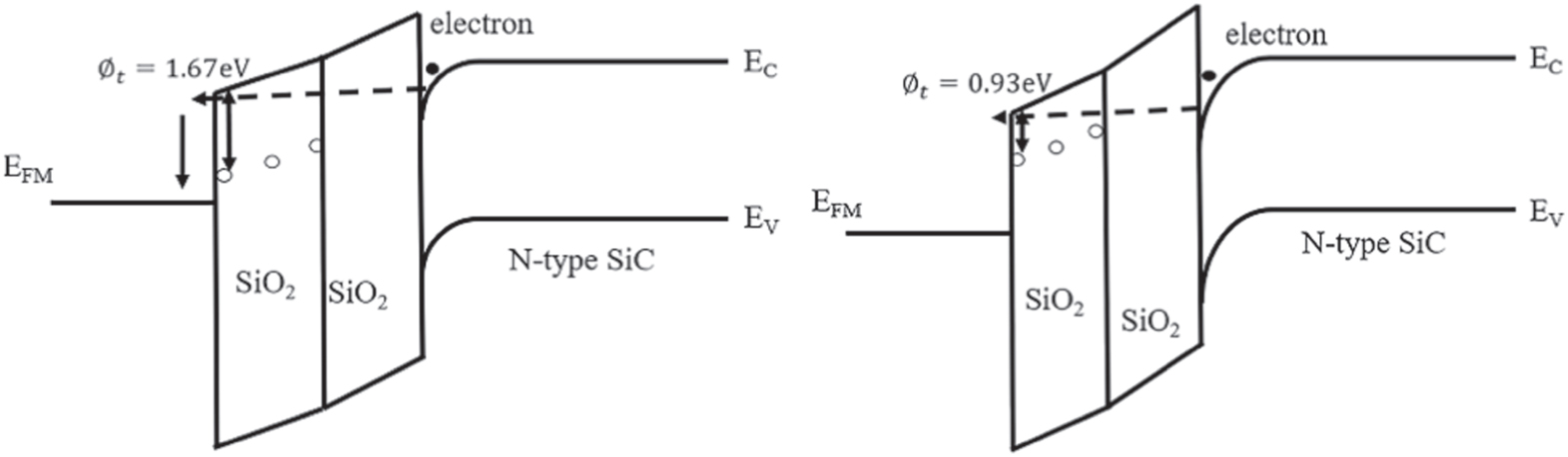
Figures 7–9 show the results of fitting the measured current using the table parameters. The energy band diagrams of the two structures are also shown in Figs. 10–13, where Figs. 10–12 are energy band diagrams of the stacked structures, and Fig. 13 is energy band diagram of the thermal oxidation layer structure. F–N tunneling is the main conduction current of thermally oxidized samples; however, the conduction current mechanism of the stacked structure is more complex. Simultaneously, the location of defects below the SiC conduction band energy level was also verified, and this also corresponded to the bulging shown in Fig. 3b.

Figure 7. Comparison between measured current density and TAT theoretical current.
Download figure:
Standard image High-resolution image
Figure 8. Comparison between measured current density and theoretical hopping conduction current.
Download figure:
Standard image High-resolution image
Figure 9. Comparison between measured current density and theoretical Poole Frenkel current.
Download figure:
Standard image High-resolution image
Figure 10. Schematic of energy band under trap assisted tunneling mechanism.
Download figure:
Standard image High-resolution image
Figure 11. Schematic of energy band under hopping conduction mechanism.
Download figure:
Standard image High-resolution image
Figure 12. Schematic of energy band under Poole-Frenkel mechanism.
Download figure:
Standard image High-resolution image
Figure 13. Schematic of energy band under Fowler-Nordheim mechanism.
Download figure:
Standard image High-resolution image
Notably, Frankel–Poole emission is also involved in the breakdown, as observed in the increased current between the electric fields within the range of 10–11 MV cm−1, as shown in the I-V curve of the stacked SiO2 in Fig. 6. A lower energy band offset might have been presented between the stacked SiO2 and 4H-SiC compared with that between thermally grown SiO2 and 4H-SiC, possibly limiting the direct usage of stacked SiO2 on the 4H-SiC surface. Summarily, the quality of the SiO2/SiC interface has been significantly improved, and the output characteristics of the device will be enhanced if the stacked SiO2 structure is applied to the device; moreover, the device threshold voltage may be small. It is a problem that complex conduction mechanisms cause current leakage. Although more complex mechanisms occur in the stacked structure, the device threshold voltage may be comparable to that of the thermal SiO2 structure.
Conclusions
In this study, a new process of thermal SiO2 and ALD SiO2 stacking structures was proposed for the first time and MOS capacitors were prepared. This process effectively reduced the interface state density at the SiO2/SiC interface compared with the process of thermal oxidation only. This stacked structure may be applicable in actual MOSFET power devices. Moreover, deep energy level traps were found in the stacked structure different from those in the thermal SiO2 structure. However, more complex conduction current mechanisms were found in the stacked structure compared with the thermal SiO2 structure. The leakage problem was perhaps the dominant issue for applications of this structure in SiC devices for high-voltage situations. Therefore, future studies should focus on methods to improve gate voltage breakdown characteristics.
Acknowledgments
This work was supported in part by the Youth Innovation Promotion Association of CAS under Grant Y201926. And we would like to thank Editage (www.editage.cn) for English language editing.