


Abstract
Polycrystalline Sb2Te3−xSex  samples were synthesized by the solid-state reaction method. The structural analysis showed that up to the maximal concentration of Se, the samples possess rhombohedral crystal symmetry (space group
  ). The increase of Se content increases the resistivity of the samples. The variation of phonon frequencies, observed from the Raman spectroscopic study, depicts an anomalous behaviour around
  . The sample Sb2Te2.8Se0.2 also shows maximum Seebeck coefficient, carrier concentration and thermoelectric power factor. The nature of the scattering mechanism controlling the thermopower data has been explored. The thermoelectric properties of the synthesized materials have been analyzed theoretically in the frame of the Boltzmann equation approach.
Export citation and abstract BibTeX RIS
Introduction
The thermoelectric (TE) effect refers to the phenomenon of direct conversion of heat to electric voltage and vice versa [1,2]. The efficiency of a TE material can be quantitatively expressed by the dimensionless term figure of merit,  , where S, ρ and κ, are, respectively, the Seebeck coefficient, the electrical resistivity and the thermal conductivity of the TE material and T is the absolute temperature. By maximizing the power factor
  and/or lowering the thermal conductivity, ZT can be improved [3,4]. Antimony telluride (Sb2Te3) is a well-known p-type TE material for near room temperature applications [5–8]. The incorporation of Se atoms into a Sb2Te3 lattice modifies the nature of defect states, which, in principle, should lead to interesting changes in its TE properties. Efforts were thus devoted to study the effect of Se doping on the structural [9], transport [10], electronic band structure [5] and TE [11] properties of Sb2Te3 alloys. Some anomalous behaviour was reported in the range
  for the Sb2Te3−xSex system, which needs further attention. On the contrary, Bi2Te3-based chalcogenides, viz., Bi2Te3−xSex, including the most compensated compound Bi2Te2Se, are well explored [12,13].
Here we investigate different compositions of the Sb2Te3−xSex  alloy. Room temperature powder X-ray diffraction (XRD) and thermal variation of resistivity,
  data show a systematic variation with the Se content. However, the S, PF, Hall carrier concentration of the charge carriers
  , and the Raman spectroscopic study show some anomalous behaviour around
  . In this report, an attempt has been made to elucidate the origin of this anomalous behaviour. In addition, the S(T),
  ,
,  and PF data have also been theoretically simulated. The evaluation of the band energy spectrum with the Se content is predicted.
Experimental
Polycrystalline Sb2Te3−xSex ( , 0.2, 0.6, 1.0) samples were synthesized by the solid-state reaction method [6]. The details of the structural characterization, the
  , S(T) measurements and room temperature Raman spectroscopic studies can be found elsewhere [6]. The temperature-dependent Hall coefficient
  measurements were performed by the van der Pauw method on similar bar samples in a closed cycle refrigerator (CCR)-based 15 T magnet supplied by Cryogenic Ltd., UK.
Results and discussion
Phase purity and structure of the Sb2Te3−xSex  mixed crystals have been identified by XRD and the corresponding spectra are shown in fig. 1(a). We have performed Rietveld refinement (utilizing the Materials Analysis Using Diffraction (MAUD) program) using atomic positions and substitutions of all the synthesized Sb2Te3−xSex (
 , 0.2, 0.6, 1.0) samples. The space group
  and point group D3d were used for the refinement [14–16]. The refinement parameters are provided in table 1. Figure 1(b) shows a typical refinement result for the Sb2Te2.8Se0.2 sample. The variation of the lattice constant with the Se content for the samples are shown in the inset. The linear contraction of the lattice parameters with increased Se concentration closely follows Vegard's law. The atomic radii of Te and Se are 142 pm and 100 pm, respectively [17]. Thus, substitution of Se at the Te position should lead to a decrease in the lattice parameter and hence the cell volume (table 1). According to Vegard's law, the crystallographic parameters of a continuous substitutional solid solution vary linearly with the concentration when the nature of the bonding is similar in the constituent phases. The XRD results thus confirm that synthesized Sb2Te3−xSex alloys are single phase in nature and a complete solid solution has been formed with Se, substituting Te. However, a close observation reveals that the variation of the lattice parameter a with the Se concentration is exactly linear, i.e., strictly following Vegard's law. However, the variation of the lattice parameter c with the Se content shows a little deviation from linearity around
  . This might be related to the anomaly observed in S(T),
  or
or  and PF data of the Sb2Te2.8Se0.2 sample discussed later.
Table 1:.
Rietveld refinement parameters, viz., lattice parameters, unit cell volume, position coordinates, site occupancy, Debye-Waller factor  , reliability parameters (
 ,
,  , and Rexp(%)), and goodness of fit (Gof or χ2) value, as obtained using MAUD software for the samples Sb2Te3−xSex (
 , 0.2, 0.6, and 1.0). The corresponding values of the estimated errors are also provided.
| Phase | Sb2Te3 [ ] ] |
Sb2Te2.8Se0.2 [ ] ] |
Sb2Te2.4Se0.6 [ ] ] |
Sb2Te2Se [ ] ] |
|---|---|---|---|---|
| Cell (Å) |  |
 |
 |
 |
 |
 |
 |
 |
|
| Cell volume | 476.25 | 472.02 | 462.36 | 451.97 |
 |
0.0 / 0.0/ 0.3994 | 0.0 / 0.0/ 0.6027 | 0.0 / 0.0/ 0.3962 | 0.0 / 0.0/ 0.3943 |
 |
 |
 |
 |
|
| Te1x/Te1y/ | 0.0 /0.0/ | 0.0 /0.0/ | 0.0 /0.0/ | 0.0 /0.0/ |
| Te1z | 0.7874(2.4 × 10⁻⁵) | 0.7879(4.0 × 10⁻⁵) | 0.7867(2.9 × 10⁻⁵) | 0.7860(3.5 × 10⁻⁵) |
| Se1x/ Se1y/ | – | Te2/ Se1: 0.0/ 0.0/ 0.0 | Te2/ Se1: 0.0/ 0.0/ 0.0 | 0.0/ 0.0/ 0.0 |
| Se1z | ||||
 |
Sb: 2.619 (0.026) | Sb: 1.1917 (0.021) | Sb: 1.8722 (0.020) | Sb: 1.544 (0.024) |
| Te1: 1.522 (0.032) | Te1: 1. 1917 (equal), | Te1: 1.8722 (equal), | Te1: 1.544 (equal), | |
| Te2: 0.147 (0.029) | Te2/Se1: 1.1917 (equal) | Te2/Se1: 1.8722 (equal) | Se1: 1.544 (equal) | |
 (%) (%) |
3.941 | 5.967 | 5.171 | 4.814 |
 (%) (%) |
3.091 | 4.617 | 4.089 | 3.819 |
 (%) (%) |
2.104 | 4.602 | 4.115 | 3.886 |
Gof or  |
1.873 | 1.296 | 1.257 | 1.239 |
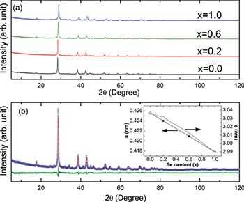
Fig. 1: (Color online) (a) X-ray diffraction patterns of the samples Sb2Te3−xSex ( , 0.2, 0.6, and 1.0). (b) X-ray diffraction pattern of the sample Sb2Te2.8Se0.2 after Rietveld refinement. The inset shows the variation of the lattice constants, a and c, with the Se composition for all the samples.
Download figure:
Standard imageFigure 2 shows room temperature Raman spectra (RS) for all the synthesized samples. The Sb2Te3 alloy exhibits four Raman active modes:  ,
,  ,
,  and
and  [18–20]. The RS (fig. 2) for Se-doped Sb2Te3 alloys depict three peaks at around
  ,
,  and
and  , that can be attributed to Raman active
  ,
,  , and
, and  vibrational modes, respectively. The active Raman mode
  (around
  ) is out of the range measured in this work [6].
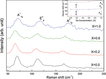
Fig. 2: (Color online) Room temperature Raman spectra of the samples Sb2Te3−xSex ( , 0.2, 0.6, and 1.0) recorded under excitation at
  , indicating the presence of Raman active
  modes. The inset summarizes the observed Raman shifts of different vibrational modes with the
  content for the synthesized Sb2Te3−xSex
  samples.
Download figure:
Standard imageAlthough the Se atom is iso-electronic with Te, it is more electro-negative than Te. The incorporation of Se atoms in the Sb2Te3 lattice will change its lattice dynamics. The inset in fig. 2 summarizes the observed Raman shifts of different vibrational modes with the Se content and reveals that all the observed Raman active modes have a very small shift with the Se doping. Since the atomic masses of Sb and Te are comparable, the observed slight variation in  ,
,  and
and  modes with the
  content is anticipated for Sb2Te3−xSex
  mixed crystals, where the Se concentration is not significantly higher. However, a close observation of fig. 2 (inset) divulges that, initially, for low Se content
  , the phonon frequencies shift to the lower wave number side. But with a further increase of Se, i.e., for
  and 1.0, the observed phonon frequencies gradually shift to the higher wave number side. The unit cell of Sb2Te3-like compounds has five quintuple layers (Te1-Sb-Te2-Sb-Te1) weakly bound by the van der Waals force in which Te atoms exhibit two different environments, i.e.,
  and
and  .
.  atoms are the centre of mass of the lattice vibration [12] and the Raman active modes directly manifest the vibrational properties of the Sb-Te(2)/Te(1) bonds. The Sb-Te2 bond is more polar than the Sb-Te1 bond. Initially for a low concentration
  , Se preferentially replaces Te at the
  site, and, subsequently, for a higher concentration (
 , 1.0) the Se atoms continue to replace Te at
  sites in a random manner [21]. This might lead to the observed anomaly in phonon frequency for the Sb2Te2.8Se0.2 sample (inset in fig. 2, marked with an arrow).
The  data of the polycrystalline Sb2Te3−xSex samples depict that ρ increases with increasing Se concentration (fig. 3(a)). Pristine Sb2Te3 always possesses over-stoichiometric Sb atoms along with native point defects, viz.,
  and segregated Te [6,22,23]. The over-stoichiometric Sb atoms occupy prevailingly the
  sites in the Te sublattice, giving rise to antisite (AS) defects of
  type. Due to such AS defects, Sb2Te3 always shows a p-type conductivity with hole concentration around
  [9]. With increasing Se concentration, the formation energy of these AS defects increases. As a consequence the formation probability of AS defects decreases, which, in turn, leads to the decrease of the carrier (hole) concentration in Sb2Te3−xSex samples with increasing x. Thus, ρ increases with increasing Se content for the reported Sb2Te3−xSex alloys.
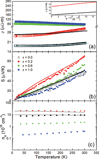
Fig. 3: (Color online) Experimental (points) and simulated (solid lines) temperature dependences of (a) the electrical resistivity ρ, (b) the Seebeck coefficient S, and (c) the Hall carrier concentration  for the Sb2Te3−xSex (
 , 0.2, 0.6, and 1.0) samples. The simulation was performed simultaneously (with the same parameters) in the frame of the Boltzmann equation approach for the samples with the
  and 0.2 Se content. The inset in (a) demonstrates the power-law fit,
  with
with  to the
  data for the Sb2Te3 and Sb2Te2.8Se0.2 samples.
Download figure:
Standard imageFigure 3(a) further depicts that while Sb2Te3 and Sb2Te2.8Se0.2 samples exhibit weakly metallic ρ, but an activated  behaviour is observed for higher-Se-content samples. The observed metallic
  data, arising due to the increase of the intrinsic carrier concentration at high temperatures, are typical for these heavily doped narrow band semiconductors [24]. In order to extract the nature of carrier scattering in Sb2Te3−xSex (
 , 0.2) samples, the
  curve is fitted with the power-law expression
  . For both the samples, the obtained best-fit value of n is 1.66. Recently Dutta et al. reported the same n value for Sb2Te3 crystals [8]. On the other hand, a similar value of
  for the Sb2Te3−xSex system was also reported earlier by Kulbachiniskii et al. [5]. For bulk Sb2Te3 and the related TI systems, the transport properties of the surface state are often mixed with the bulk state, which probably gives rise to the unusual value of the exponent in the low-Se-content Sb2Te3−xSex samples [6,8].
The S(T) data depict that all the reported samples are of p-type in nature (fig. 3(b)). S(T) initially increases with increasing x from  to 0.2. But for
  , S(T) decreases. The compositional dependence of the scattering parameter
  is estimated from the S(T) data. For a heavily doped semiconductor (for a single valley in the isotropic case), S is given by [13]

Here  is the reduced Fermi energy; the parameter r describes the energy dependence of the scattering time, and
is the Fermi integral. Now,  corresponds to the acoustic phonon scattering,
  is the scattering due to optical phonons and
  denotes the scattering by ionized impurities. We estimate the Fermi energy
  in two samples, viz., Sb2Te3 and Sb2Te2.8Se0.2, exhibiting metallic behaviour by a simple model,

where  is the carrier concentration (fig. 3(c)). Reasonable values of
  and 120 meV are obtained, respectively, for
  and 0.2 samples [25,26]. Using these Fermi energies and formulae (1) and (2) we may estimate the scattering parameter r. Such procedure yields
  and
and  , respectively for
  and
and  alloys. The obtained best-fit value of
  for Sb2Te3 alloy (i.e.,
  ) corroborates the reported results [13]. The S(T) data thus reveal that in SbTeSe-based degenerated semiconductors, the increase of the Se content shifts the scattering from the preferentially acoustic phonon closer to impurity scattering.
For the Sb2Te2.4Se0.6 and Sb2Te2Se samples, the activation energy  is estimated from the
  data using the relation
where  is a constant. The estimated
  values, 9.24 meV and 12.30 meV respectively for Sb2Te2.4Se0.6 and Sb2Te2Se, indicate that the estimated transport gap
  is much smaller than the reported band gap
  [27].
[27].  arises due to the difference between the lower conduction band (LCB) and the upper valence band (UVB) [22]. However, according to Akrap et al., while
  is determined by the band structure,
  is actually linked to the presence of point defects [13]. Sb2Te3 hosts various kinds of defects, viz., AS defects of
  type,
type,  and segregated Te. Increasing the Se content in the Sb2Te3 matrix enhances the interplay between these defects with Se atoms initially replace
  atoms, but for a higher concentration it continues to replace
  atoms randomly. This might lead to the observed change from a metallic to an activated behaviour in the
  data for x > 0.2. The energy state due to the native defects in the Sb2Te3−xSex system probably lies between LCB and UVB and leads to a smaller
  in the activated samples. Further, when the composition is tuned from Sb2Te3 to Sb2Te2Se, the concentration of holes in the system decreases. Around the composition x = 1 (Sb2Te2Se), the Se/Te sublattice is expected to be ordered with an almost complete compensation of donor and acceptor impurities [13]. Therefore, around x = 1 the bulk conductivity should be minimum, which is correctly reflected in our
  data (see fig. 3(a)).
Figure 3(c) represents the thermal variation of  data for all the Sb2Te3−xSex samples, measured in a magnetic field of 12 T. Like the S(T) data initially with increasing x,
  increases for Sb2Te3 and Sb2Te2.8Se0.2, but for
  , it decreases, indicating that the apparent hole concentration is highest in Sb2Te2.8Se0.2. Here we would like to present a plausible explanation for such anomalous behaviour of
  in Sb2Te3−xSex. The band structure calculation indicates that the UVB of Sb2Te3 consists of six ellipsoids and the lower valence band (LVB) is known to be multivalleyed [5,24]. While explaining the Shubnikov-de Haas (SdH) and transient thermoelectric effect (TTE) data for the Sb2Te3−xSex
  system Kulbachinskii et al. indicate the presence of another valence band (NVB) for
  and clearly predict two different regions, viz.,
  and
and  in the band structure [5]. In the first region
  , only UVB and LVB contribute. But in the second region
  the contribution comes from UVB, LVB and NVB, where NVB moves up and UVB moves down due to Se doping. It should be mentioned that UVB and LVB are not equally populated, the ratio of the density of holes in LVB to that of UVB is around 390 [28]. In view of this large ratio, LVB contributes mostly in the conduction mechanism. The evaluation of the band structure with the Se content in the Sb2Te3−xSex
  alloy as predicted by Kulbachinskii et al. [5], and correspondingly the net contribution of the carrier from UVB, LVB and NVB might be related to the experimentally observed
  behaviour.
In the framework of the Boltzmann equation approach, we simulated simultaneously (with the same parameters)  (see fig. 3(a)), S(T) (see fig. 3(b)), and
  (see fig. 3(c)) for the samples with
  and 0.2. Theoretical dependences are shown in fig. 3(a)–(c) by solid lines. However, we were unable to reproduce a small value of the Seebeck coefficient in samples with
  and
and  Se content without an unrealistic change of the band parameters. We suggest that part of holes in the material is localized and to fit data for samples with high Se content the localization of part of the holes should be taken into account. The theoretical model and the method of calculation are described in ref. [5]. In the fitting following scattering mechanisms were taken into account: acoustic phonon scattering, ionized acceptors scattering, grain boundary scattering. All acceptors were assumed to be ionized. Other parameters, viz., effective masses, band edges, deformation potential, acceptor concentration, etc., are taken from the literature. For the fitting of the sample with
  Se content, only the position of the second valence band, grain size and acceptor concentration were changed with respect to Sb2Te3. The details of the simulated parameters are provided in table 2. The optimal fitting value for the distance between valence bands is larger than the one that was experimentally obtained earlier [28]. This is probably due to the localization of the part of the holes in the investigated samples. This could be also origin of the very small Seebeck coefficient in the samples with
  and
and  . For these samples (
 , 1.0) the localization of the part of the holes can explain the
  data, which has an activated character (see fig. 3(a)). These samples have too large value of the Hall coefficient and a small value of the Seebeck coefficient. One of the reasons may be (probably) due to modification of the band structure with high Se content [5] and localization of the part of the holes.
Table 2:. The simulated parameters of the investigated Sb2Te3 and Sb2Te2.8Se0.2 alloys obtained by fitting the experimental temperature dependences of the Seebeck coefficient, the resistivity, and the Hall carrier concentration.
Sb2Te3 [ ] ] |
Sb2Te2.8Se0.2 [ ] ] |
|||
|---|---|---|---|---|
| Bandgap (eV) | 0.25 | 0.25 | ||
| Second valance band (eV) | 0.19 | 0.08 | ||
Effective masses  |
Light Holes | 0.043 | 0.043 | |
| Heavy Holes | 0.15 | 0.15 | ||
| b1 | 0.705 | 0.705 | ||
| Light Holes | b2 | 0.615 | 0.615 | |
| Band extrema positions (b) | b3 | 0.615 | 0.615 | |
| b1 | 0.534 | 0.534 | ||
| Heavy Holes | b2 | 0.341 | 0.341 | |
| b3 | 0.341 | 0.341 | ||
Acceptor concentration  |
 |
 |
||
| Scattering parameters | Density (kg/m3) | 6500 | 6500 | |
| Sound velocity (m/s) | 1780 | 1780 | ||
| Deformation potential (eV) | 3 | 3 | ||
| Grain boundaries | Grain size (nm) | 15.3 | 10 | |
| Scattering constant | 0.3 | 0.3 | ||
| Dielectric constant | 101 | 101 |
Figure 4 shows the compositional dependence of PF for the Sb2Te3−xSex samples estimated from the measured quantities. The theoretical values of PF for the Sb2Te3 and Sb2Te2.8Se0.2 alloys, calculated from the simulated S(T) and  data, are also plotted in fig. 4. The PF increases with increasing temperature and reveals a non-saturating behaviour around room temperature. Similar to the behaviour observed for the S(T) and
  data, the maximum value of PF is also observed for the Sb2Te2.8Se0.2 alloy. This further indicates that increasing the Se content in Sb2Te3 does not always contribute a positive role in increasing the thermoelectric performances of Sb2Te3−xSex samples. However, conclusive evidence can be drawn only after estimating ZT. It should be recalled that Sb2Te2.8Se0.2 possess the highest
  . It is thus quite justified to assume that tuning of the carrier concentration as well as band structure engineering including the optimization of the band parameters in the Sb2Te3−xSex system should play a crucial role in obtaining a good TE material.
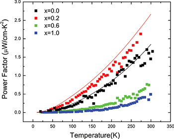
Fig. 4: (Color online) Thermal variation of thermoelectric power factor for the Sb2Te3−xSex ( , 0.2, 0.6, and 1.0) samples. Points denote experimental data and solid lines represent the theoretical fit.
Download figure:
Standard imageConclusion
XRD data and Raman spectra confirm that all the synthesized Sb2Te3−xSex samples exhibit rhombohedral crystal geometry. It has been realized that the surface states are often mixed with the bulk state, giving rise to the observed metallicity in the Sb2Te3 and Sb2Te2.8Se0.2 samples. The transport gap  , estimated in high-Se-content samples showing an activated behavior, is smaller than the reported band gap
  probably due to the presence of point defects and of the tail of the density of state. Acoustic phonon scattering dominates the S(T) data for the synthesized host Sb2Te3. However, with increasing Se concentration, impurity scattering gradually dominates the S(T) data. The theoretical calculation, based on a four-band model, demonstrates that the position of the second valance band as well as the acceptor concentration are sensitive to the Se concentration and to the part of the holes in high-Se-content samples is localized.
Acknowledgments
The work is supported by DST, Government of India-RFBR, Government of Russia (DST reference No.: INT/RUS/RFBR/P-183; RFBR grant: IND-a 15-52-45037). The financial grant, including the fellowship of the first author DD, received from the UGC-DAE Consortium for Scientific Research, Kalpakkam node (Project reference No.: CSR-KN/CRS-65/2014-15/505) is also gratefully acknowledged. The authors would also like to thank the DST, Government of India, for low-temperature high-magnetic-field facilities at UGC-DAE CSR, Kolkata Centre.