


Abstract
In this work, the radio frequency magnetron sputtering technique (RF sputtering) was utilized for the deposition of Y2O3-doped zinc oxide (ZnO) thin films on a SiO2 substrate. The microstructures and optical properties of the thin films deposited utilizing various gas (Ar:O2) ratios at 400 °C were characterized. XRD investigation of thin films demonstrates that all deposited films are polycrystalline and there is a single phase hexagonal wurtzite type structure with a strong (002) orientation. An increment of O2 in the gas mixture reduces the intensity of peak (002). Y2O3-doped ZnO thin films exhibited denser morphology with refined microstructure as compared to pure ZnO films. The absorbance and transmittance of doped ZnO thin films were measured by UV-VIS-IR spectrophotometer in the wavelength range 300 nm to 800 nm. High transmittance in the visible region and high band gap of films were revealed. Photoluminescence (PL) of films was estimated at the excitation wavelength of 325 nm and it uncovered two PL peaks present in UV and visible regions (400 nm to 445 nm). The effect of Ar:O2 gas proportion on stoichiometry, structural and optical properties of the Y2O3-doped ZnO thin films was also revealed.
Export citation and abstract BibTeX RIS
Introduction
Some potential materials of II–VI group semiconductors have stood out of research network for a conceivable substitution of GaN as UV sources. Especially, ZnO is popular for its utilization in the fields of microelectronics [1] and surface acoustic wave devices [2]. Nanostructured zinc oxide is one of the promising optoelectronic materials which has potential applications in solar cells, gas sensors, antibacterial and UV protective coatings, lubricants, concrete manufacturing, etc. ZnO thin films have been utilized in various optoelectronic devices because of their large exciton binding energy of 60 meV and high energy band gap of 3.37 eV at normal temperature. ZnO thin films are used as shielding materials for transparent electromagnetic interference as well as window layers in solar cell production. Crystallization of ZnO occurs in three structures such as hexagonal wurtzite, cubic zinc blende and cubic rocksalt material. Exceptionally nonlinear current-voltage characteristics and a high energy absorption capability are main identifications of ZnO-based varistors. Subsequently, they are generally utilized as surge absorbers in electronic circuits, gadgets and electrical power systems for protection against perilous over-voltage floods. Nonlinear characteristics of voltage-current of ZnO-based varistor ceramics appear due to evolution of double Schottky barriers at the grain boundaries. There is recent report that breakdown voltage and energy characteristics of varistor components can be essentially extended by the incorporation of Y2O3 and other rare-earth oxides for components of varistor ceramics [3].
Y2O3-doped ZnO has pulled in a great deal of interest because of its remarkable optical and electrical properties. As referenced in a past report by Bernik et al. [4], an increase in threshold voltage from 150 to 274 V as well as the increase of leakage current with the addition of Y2O3 in ZnO encouraged the study of microstructure and electrical properties of Y2O3-based ZnO varistors. The yttria-doped ZnO films reveal high absorption coefficient and its optical properties are firmly dependent on the thickness of the films [5]. The band gap values of yttria-doped ZnO films reported in the literature from 2.0 eV up to 3.7 eV have been prepared by various deposition methods, such as sputtering, laser ablation and thermal evaporation [6]. Optical and electrical properties of Sc-doped ZnO thin films by DC magnetron sputtering were investigated by Minami et al. [7]. Kaur and Mehra et al. [8,9] have performed in detail structural, electrical investigation of Y-doped ZnO films. They reported optical properties but focused only on the transmittance. Yu et al. [10] have reported structural, electrical, and photoluminescence (PL) characteristics of yttrium-doped ZnO films. Based on literature reports, for the first time the effect of the various Ar:O2 sputtering gas ratios on the optical properties of Y2O3-doped ZnO thin films has been investigated in the present work. The optical energy gap (Eg) and photoluminescence of the films are measured at excitation wavelength.
Experimental work
In this study, Y2O3-doped ZnO thin films were deposited on SiO2 substrate in the argon (Ar) and oxygen gas atmosphere (99.99% purity), utilizing the RF sputtering process technique. The solid-state reaction method was utilized for the preparation of the Y2O3-doped ZnO target via mixing of Y2O3 (99.99% purity) and ZnO (99.98% purity) powders in proportion, 1:50 for 2% Y2O3-doping. The powders were appropriately mixed by grinding them in an agate mortar for 6 hours. Few drops of polymer solution of polyvinyl alcohol binder were used as a binding agent and mixed properly. The powder was squeezed into a circular disk of 20 mm diameter and 5 mm thickness. This disk pellet was heated at  for 1 h to evaporate binder from pellet. Then, this circular disk was sintered at
  for 3 hours in the air to prepare the target of Y2O3-doped ZnO. The films were deposited on SiO2 substrates at different sputtering gas ratios Ar:O2, measured in units of standard cubic centimeters per minute (SCCM), with steady power of 80 watt for 3 hours under
  pressure of sputtering gas. The sputtering procedure was performed in various Ar and O2 atmospheres with a deposition time of 3 hours. The deposition time was kept consistent for each sample. Separation between target and substrate was
  , and the various sputtering gas ratios of Ar:O2 were 20:0, 15:5, 10:10, 5:15 and 0:20. The enhanced parameters such as pressure and temperature of deposition conditions of thin films are given in table 1.
Table 1:. Sputtering deposition parameters and materials used.
| Description | Value or parameter |
|---|---|
| Target prepared | Y2O3-doped ZnO |
| Substrate used | SiO2 |
| Base pressure |  |
| Working pressure |  |
| Power supplied | 80 W |
| Distance between target | 4.5 cm |
| and substrate | |
| Temperature |  |
| Deposition time | 3 h |
Results and discussions
Figure 1(a) represents the XRD plot of Y2O3-doped ZnO pellet sintered at 1000°C. The XRD peaks of thin film deposited on the SiO2 substrate in Ar:O2 atmosphere at 400°C are shown in fig. 1(b). The film is a polycrystalline with hexagonal (wurtzite) structure as observed from XRD patterns of fig. 1(b). It is evident from this figure that the intensity for the entire plane was the highest for Y2O3-doped ZnO. The peak at (002) plane dominates over other peaks clearly indicating the orientation of thin films or pellet along the c-axis. The growth patterns of the Y2O3-doped ZnO thin films were at right angles to SiO2 substrate. The polycrystalline films with hexagonal (wurtzite) structure were found for pellet and doped thin films in the range of 20–80°. The major peak (002) was observed at 34.4°  for both Y2O3-doped ZnO thin films and pellet.

Fig. 1: (a) XRD pattern of Y2O3-doped ZnO pellet sintered at 1000°C. (b) XRD pattern of Y2O3-doped ZnO film deposited by RF sputtering.
Download figure:
Standard imageThe average crystallite size of the thin film deposited on SiO2 substrate has been evaluated using the following well-known Scherer equation [11]:

where  is the full width at half maximum, i.e., the broadening of diffraction line determined at half of its maximum intensity,
  is the wavelength of X-rays for Cu Kα target (
 ), and
  is the Bragg's angle of diffraction of the peak (002). Lattice spacing d for the hexagonal lattice is given by the following expression:

where a, c are the lattice constant and h, k, and l are Miller indices of the plane for the hexagonal unit cell. Lattice constants a and c are computed with the help of eq. (2) and mentioned in table 2.
Table 2:. Variation of grain size, FWHM, d-spacing and lattice parameter for doped and undoped ZnO thin film deposited on SiO2 substrate.
| Name | h k l |  |
FWHM | d-spacing (Å) | D (nm) | Lattice parameter (c) |
|---|---|---|---|---|---|---|
| ZnO + Y2O3 (pellet) | 0 0 2 | 34.513 | 0.108 | 2.596 | 27.73 | 5.193 |
| ZnO + Y2O3 (thin films) | 0 0 2 | 34.437 | 0.159 | 2.602 | 18.02 | 5.204 |
AFM was used to examine the surface configuration of Y2O3-doped ZnO thin films. Figure 2(a) shows the two-dimensional AFM image of the sample deposited on SiO2 substrate. The anisotropic grain development in thin films might happen because of various factors, for example, orientation-dependent grain boundary mobility, favoured orientation of the grains, grain boundary free-energy and residual stress. As shown in the 3D image of fig. 2(b), the uniform and homogeneous crystallite distribution leads to enhanced film transparency. Figure 2(c) shows the histogram of AFM image. The average roughness of 13.147 nm with RMS 17.385 nm was observed for Ar:O2 gas ratio of 15:5. The field emission scanning microscopic examination was conveyed for the surface morphology of Y2O3-doped (2%) ZnO thin films and a micrograph is shown in fig. 2(d). Extremely fine grains averaging around 32 nm are observed and grains are distributed equitably with high uniformity throughout the films. The uniform distribution is the consequence of controlled preferential nucleation of the grains driven by RF sputtering process. The films have uniform density and are made out of arbitrarily oriented grains. The grains are very fine and progressively spread in thin films developed with lower Y2O3 concentration. The grain size expands and the shape of the grains becomes round and hexagonal with increasing precursor concentration as observed in fig. 2(d) for Ar:O2 ratio of 15:5.

Fig. 2: (a), (b) 2D and 3D AFM images; (c) histogram; (d) FE-SEM of Y2O3-doped ZnO thin film deposited on SiO2 substrate for Ar:O2 ratio of 15:5 at 400°C.
Download figure:
Standard imageFigure 3(a) shows optical absorption spectra of Y2O3-doped ZnO films as a function of wavelength of range 300–800 nm at various Ar:O2 ratios. The optical absorbance for different Ar:O2 ratios (20:0, 15:5, 10:10, 5:15, 0:20) between 0 and 50% in the near-UV region ranges from 400 nm down to 300 nm. Defect energy states are responsible for the absorbance less than 50% below the energy band gap. It is observed that absorption near edge shifts towards longer wave lengths with rising Ar:O2 proportions, indicating decline in the band gap. Figure 3(b) shows optical transmittance spectra in the wave length 300 to 800 nm and high average transmittance in the visible range is accomplished for different Ar:O2 gas ratios. There is transparency of films in the visible part of spectrum with a sharpened absorption edge at around 375 nm of wavelength, which is near the energy band gap of ZnO (3.31 eV). Average optical transmittance values of doped ZnO films for different Ar to O2 ratios are observed around 90% in the visible spectrum; however it is more than 90% for films with Ar to O2 ratio 20:0. These bands demonstrated a significant distinct interference fringe pattern, depicting the fine surface of thin films. Curve or wavy-like transmittance of films elsewhere from natural absorption edge is due to interference emerging from the substrate-film and film-air interfaces [11]. There is no transmission up to 360 nm and clear fringes are viewed in the wavelength range of 425–800 nm for films. However, the clearness of the fringes continues to diminish with the reducing Ar:O2 ratio, which might be because of the expansion of surface roughness. Transmission of films begins at about 375 nm except for the film at Ar:O2 proportion of 20:0 for which it starts at a little bit lower wavelength. Transmittance of film requires to rely upon a few factors such as surface roughness, oxygen inadequacy and impurity points. Figure 4 shows reflectance spectrum in the spectra range of 300 to 800 nm. It is obvious from this figure that the reflectance is very low for all films of various Ar:O2 proportions. The variety in reflectance might be a direct result of the structural change in films, since perspective proportion of crystallites varies with diminishing sputtering Ar:O2 gas proportions.

Fig. 3: (a) Wavelength vs. absorbance; (b) wavelength vs. transmittance spectra of Y2O3-doped ZnO thin films deposited on SiO2 substrate with different Ar to O2 ratios at 400°C.
Download figure:
Standard image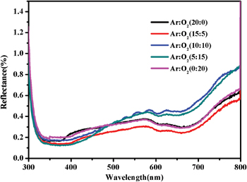
Fig. 4: Wavelength vs. reflectance of Y2O3-doped ZnO thin films deposited on SiO2 substrate at 400°C.
Download figure:
Standard imageRelationship among the band gab, absorption coefficient  and incident photon energy (hν) based on the optical transmission theory is given by the equation

where A is constant, Eg is band gap in eV and n is the index describing the type of transition, the value of n is  for allowed direct transitions,
  for allowed indirect transitions [12,13]. The optical band gap of thin films for different Ar, O2 ratios was calculated. Direct energy band gaps of the various films were determined from the
  vs. hν (Tauc model) plot [14,15] by extrapolating a linear fit to
  as shown in fig. 5. Existence of linear behavior
  with
with  in a certain range shows that Y2O3-doped ZnO thin films are in the category of direct semiconductors. The determined energy band gap of different thin films varies in the range from 3.038 eV to 3.366 eV. The observed band gap values are almost expanded by rising the concentration of Ar gas. Energy band gaps of Y2O3-doped ZnO thin films deposited at different Ar:O2 ratios are as follows: for 0:20 (3.061 eV), 5:15 (3.038 eV), 10:10 (3.055 eV), 15:5 (3.169 eV), and 20:0 (3.366 eV). The dependency of optical energy gap on Ar pressure is correlated with the crystallinity of the film. It is sensible to accept that the broadening of the energy band gap is due to decreased crystallinity of thin films. As sputtered atoms lose kinetic energy with increase of Ar pressure, the fraction of amorphous ZnO increments. Numerous authors suggest that the amorphous phase in these films is the main reason behind the increased value of band gaps. Photoluminescence (PL) is the emission of light after the absorption of electromagnetic radiation. The information that can be derived from PL is energy band gap, defects in the films and the feature of the deposited films. A photoluminescence spectrometer comes with an ozone-free xenon arc lamp that covers a range from 250 nm to
  for steady state measurements and the spectrometer also includes laser Nd:YAG (266 nm) source for PL measurements. Figure 6 shows PL spectra for various deposited thin films. Room temperature PL emission for Y2O3-doped ZnO thin films with different (Ar:O2) sputtering gas ratios 20:0, 15:5, 10:10, 5:15, 0:20 were performed in the wavelength scope of 300 to 600 nm and at the excited wavelength of 330 nm. All PL spectra of films with sputtering gas ratios revealed a physically wide peak at about 389 nm with another secondary emission of less intensity at 400 to 445 nm. The maximum intensity of PL emission was noticed for sputtering gas Ar:O2 ratio of 15:5 out of 20:0, 10:10, 5:15, and 0:20. The defects that are produced due to different Ar:O2 gas proportions firmly influence the PL emission. The peak for wavelength from 350 to 450 nm for various films might be caused by the Zn vacancies [16,17]. The PL outcomes are in great concurrence with the past reports on thin films [18].

Fig. 5: Calculation of energy band gap energy of Y2O3-doped ZnO thin films deposited on SiO2 substrate with different Ar to O2 ratios at 400°C.
Download figure:
Standard image
Fig. 6: PL bands of Y2O3-doped ZnO thin films deposited on SiO2 substrate with different Ar to O2 ratios at 400°C.
Download figure:
Standard imageConclusion
Y2O3-doped ZnO thin films with various Ar:O2 ratios deposited by RF sputtering are polycrystalline in nature with hexagonal (wurtzite) structure. The dominating peak at (002) planes over other peaks indicated the orientation of thin films along the c-axis. The surface contour studied from AFM and FE-SEM images illustrated uniform grain growth with high uniformity throughout the films. Small values of average and RMS roughness indicated fairly smooth surface of thin films. The grain size was expanded and the shape of the grains became round and hexagonal with increasing precursor concentration. The deposited thin films exhibited great optical features, and fairly high optical transmittance in the visible spectrum. Clarity of wavy-like transmittance of films away from natural absorption edge continued diminishing with the reducing Ar:O2 ratio. The observed band gaps were almost expanded by rising concentration of Ar gas and they varied in the range from 3.038 eV to 3.366 eV. High estimations of optical transmittance showed the utilization of Y2O3-doped ZnO thin films for transparent window layers of photovoltaic cells. Photoluminescence of Y2O3-doped ZnO thin films showed sharpened peaks in the visible as well as ultraviolet regions which made them useful for opto-electronic applications.