Analysis and Implementation of High-Performance DC-DC Step-Up Converter for Multilevel Boost Structure
 M. Premkumar
 C. Kumar
 R. Sowmya
- 1Department of Electrical and Electronics Engineering, GMR Institute of Technology, Srikakulam, India
- 2Department of Electrical and Electronics Engineering, Bannari Amman Institute of Technology, Sathyamangalam, India
- 3Research Scholar, Department of Electrical and Electronics Engineering, National Institute of Technology, Tiruchirapalli, India
The conventional DC-DC converters such as SEPIC, boost converter, etc. produces large voltage ripples in multilevel converter systems. For that reason, in this paper, a new DC-DC converter topology is proposed, and the performance is analyzed. Since the proposed converter delivers high conversion efficiency, it can be selected for multilevel boost DC-DC converters. The adverse effects such as inductor resistance and inductor size of the conventional converters are overcome by the proposed converter. The output voltage ripples are reduced in the proposed converter, i.e., the spikes in the converter output voltage are almost zero. The theoretical analysis is presented in this paper, which speaks about the advantage of the proposed converter. The converter operation is analyzed and discussed in continuous conduction mode (CCM). The voltage gain of the proposed converter is higher than the conventional boost converter. To validate the performance of the proposed converter, an experimental prototype is fabricated and tested in the laboratory. The performance of the converter is compared with the conventional boost and SEPIC converter. The experimental result confirms the theoretical analysis. The proposed converter can be extended by connecting more number of voltage multiplier (VM) cells to get the desired multilevel output voltage.
Introduction
The conventional boost dc-dc converter has several issues such as power loss, the voltage drop across various devices, and the effects due to the inductor resistance when it tries to achieve the required voltage gain. The quality of operation and the conversion efficiency is affected by the high duty cycle of the semiconductor switch (Premkumar et al., 2018a; Premkumar and Sumithira, 2019a). These problems are solved by introducing the new converters such as Zeta, SEPIC, and Cuk converters (Banaei and Bonab, 2016). The various converters are reported in Amir et al. (2019), and these converters are differentiated based on the switching methods (switching between the capacitor and inductor), and boosting techniques such as voltage multiplier (VM), voltage doubler, cascade connections, etc (Chen et al., 2018; Pop-Calimanu et al., 2019). Each of the converters has its drawbacks, and these drawbacks motivate the researchers to work on the new converters for the multilevel boost structure. For instance, the multilevel converters with conventional boost, Cuk, and SEPIC have output voltage ripples (Babaei et al., 2013; Selwan et al., 2015; Premkumar et al., 2018b).
The conventional buck-boost and boost converters are frequently preferred in solar photovoltaic systems, and fuel-based energy systems (Divakar et al., 2008; Kaouane et al., 2015; Premkumar et al., 2018b; Rosas-Caro et al., 2018a,b; Premkumar and Sumithira, 2019b). The authors in Kaouane et al. (2015) and Premkumar and Sumithira (2019b) reported converters with two MOSFET switches and hybrid boost, respectively, for solar photovoltaic (PV) systems to improve the output voltage gain along with the proper tracking technique. The quadratic buck-boost converter was reported by Rosas-Caro et al. (2018b) with the conversion output voltage and continuous input current with positive polarity.
The authors in Divakar et al. (2008) reported soft switching techniques such as zero voltage switching and zero-current switching to decrease the switching losses in the traditional boost converter. The authors in Hegazy et al. (2012) and Rosas-Caro et al. (2018a) reported the converters with the interleaved structure to achieve the required output voltage with the continuous input current. However, the interleaved structure is complicated when compared to the conventional boost converter. Besides, the author in Zeng et al. (2019) reported that the interleaved structure also helps to increase the conversion efficiency, and reduce the output voltage ripple. When the conventional interleave based boost or buck-boost converters are chosen for multi-level boost converters, it introduces a heavy spike in inductor current and the output voltage. The same can be observed from the experimental waveforms of the literature reported in Rosas-Caro et al. (2018a) and Hegazy et al. (2012).
The SEPIC converter is one of the conventional dc-dc converter derived from the traditional boost converter. Related to conventional boost converter and Cuk converter, the SEPIC converter has few ripples in the output current since the second inductor in the SEPIC converter smooths the current spikes. The SEPIC converter can be preferred in different applications such as PV system, fuel cell-based systems, and also multi-port converters (Saravanan and Babu, 2015; Buticchi et al., 2019). As a result, the SEPIC converter can be used for most of the renewable energy systems. Though the SEPIC converter voltage gain is less, and it can be used for step-up applications (Kircioglu et al., 2016; Shamshuddin et al., 2017; Premkumar et al., 2018c; Natarajan et al., 2019; Yousri et al., 2019). The voltage gain of the SEPIC converter is less than the conventional boost converter per duty ratio. The voltage gain of the SEPIC converter and boost converter is equal to D/(1-D), and 1/(1-D), respectively (Park et al., 2010; Ansari and Moghani, 2019). If the structure of the SEPIC converter is slightly modified, it may step-up voltage than the conventional boost converter. Therefore, in this paper, a modified structure for the SEPIC converter with high-quality output is discussed and examined.
A new structure is proposed for the SEPIC converter is proposed in this paper, and the converter is based on the traditional SEPIC converter. The major highlight of the proposed SEPIC converter is not having an extra parasitic element compared to the traditional SEPIC converter. A new structure is derived in a way such that a reduction in output voltage ripple and an increase in conversion efficiency. Moreover, the voltage gain is equal as the traditional boost dc-dc converter and higher than the conventional SEPIC converter with less effect of the inductor resistance. Another notable highlight of the proposed converter is its spike-free voltage and current waveforms. The efficiency of the converter is >95% when the duty ratio of the switch is <60%, >92% when the duty cycle of the switch is between 60 and 80%, and this advantage makes the converter a decent choice for the multi-level boost structure powered by the PV modules and fuel cells. The converter can also be extended to achieve high voltage gain by using elements such as inductors, diodes, and capacitors. The structure of the paper is as follows. Section Operation of the Proposed SEPIC Converter for Multi-Level Structure presents the operation of the proposed converter. The steady-state analysis under continues conduction mode (CCM) is performed in section Steady-State Analysis and Converter Comparison. The experimental results and further discussion are given in section Results and Further Discussions. The paper is concluded in section Conclusion.
Operation of the Proposed SEPIC Converter for Multi-Level Structure
The converter proposed in this paper has high-quality output and high gain by making a small modification in the conventional SEPIC converter, as shown in Figure 1. In the proposed converter, the charging capacitor is changed its position, and the gain equation is altered accordingly. The proposed converter comprises one MOSFET switch, two capacitors such as the coupling capacitor (Cs), and the output capacitor (Cout), two inductors, namely L1 and L2, and one diode. For simplified analysis, the converter operation in CCM is divided into two modes of operation. Theoretical waveform is depicted in Figure 2.
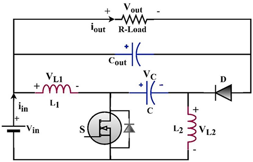
Figure 1. Schematic of the proposed converter.
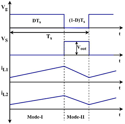
Figure 2. Theoretical waveform for the proposed converter under CCM.
The following are the assumptions made to streamline the converter examination.
• The various apparatuses of the converter are ideal. The forward drops of the switch and diode, on-state resistance (Rds−ON) of the MOSFET switch, the equivalent series resistance of the inductors, and capacitor are ignored.
• The capacitance values of the capacitors Cs and Cout are considered as high. Thus, the capacitor voltage is supposed to be constant during one switching cycle.
Mode-I
The current flow is depicted in Figure 3A. The analysis of the proposed converter is made by assuming the ideal components, and the converter is operated at CCM.
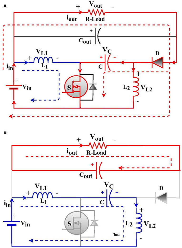
Figure 3. Modes of operation; (A) Mode-I; (B) Mode-II.
During this mode, the MOSFET switch is turned on by applying the pulse-width-modulated (PWM) signal to the gate terminal of the switch. When the switch is turned on, the current starts to flows the components such as C, L1, and L2. In Figure 3, the inductor currents are represented as iL1, and iL2, and the voltage across the coupling capacitor is represented by Vc. During mode-I, the diode is turned off due to the reverse voltage. There are three loops for energizing the storage components. The voltage across the inductor-1 (VL1) is equal to the input source voltage (Vin) which rises the current in L1. The source voltage also delivers the energy to the L2 and the coupling capacitor (C) through the load. It is observed that the second and third loop is formed by the source voltage, C, and L2. The voltage across the diode is equal to the voltage across the capacitor. The voltage across the inductor L1 is presented in Equation (1), and other expressions are written as follows.
Mode-II
The current flow during this mode is depicted in Figure 3B. During this mode, the MOSFET switch is turned off. Due to this, there are two loops in the converter operation. The coupling capacitor is energized through the inductors L1 and L2. Both the inductors start to release the energy during this mode. The inductor L2 also discharges, and the output capacitor delivers the load current. The voltage stress of the MOSFET switch is equal to the difference between the voltage across the inductor L1, and the source voltage. Various output equations during mode-II are presented as follows.
Steady-State Analysis and Converter Comparison
The steady-state analysis of the proposed converter is presented under the CCM operation. The voltage conversion of the proposed converter is the most significant parameter, and the same can be obtained from the above-two operating modes of the converter. The energy balance in the proposed converter is achieved by the charging and discharging cycle of the inductors L1 and L2. The average voltage of the inductors over one switching cycle is zero. The average voltage of the inductor is derived from the above-said equations. The average voltage equation is presented in Equations (9, 10).
From Equations (9, 10), the voltage across the capacitor, and the voltage gain of the converter being stated in Equations (11, 12).
As seen in Equation (12), the voltage gain of the proposed converter is similar to the traditional boost converter. Therefore, the proposed converter can be compared with conventional SEPIC and Cuk converters. The converters can be analyzed based on the current stress and voltage stress on the MOSFET switch under DCM and CCM operation, voltage gain, and the minimum inductance requirements. Table 1 shows the essential parameters of the converter and the other conventional converters.
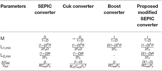
Table 1. Assessment of the proposed modified SEPIC converter with the traditional converters.
The voltage stress on the MOSFET switch and the diode is obtained based on the modes of operation. The voltage stress on the diode is presented in Equation (13).
During mode-II, the MOSFET switch is turned off. Thus, the voltage stress on the MOSFET switch is presented in Equation (14).
The energy balance is obtained between the input and the output by the inductor elements. Based on the volt-second balance equation, the current through the inductors iL1 and iL2 are calculated as follows, and further, the current stress on the MOSFET switch is obtained.
From Equation (15), the current through the inductors are obtained as follows.
Based on the above-said equations, the current stress on the diode and the MOSFET switch is obtained as follows.
The inductor current oscillates between the minimum and maximum value depends on the inductance, and it is considered as the essential element in the converter design. Thus, the current ripple of the inductor and its respective inductance is calculated by considering the operating stages of the converter. The peak-peak ripple current over one switching period is calculated as follows.
The values of the inductances decide the boundary between DCM and CCM operation of the proposed converter. By assuming the minimum inductor current (IL, min) is zero, the minimum inductance of the inductors is calculated as follows.
Where ΔIL is the current ripples of both the inductors, and it is given by (DTs/L)Vs. The peak-peak output voltage ripples of the proposed converter can be obtained by the differential equations. Since the proposed converter has two capacitors, the output voltage can be written as follows.
Results and Further Discussions
The proposed converter, and the traditional converters such as SEPIC converter, and Cuk converters are simulated using MATLAB/Simulink software. To check the effectiveness of the proposed modified SEPIC converter, an experimental prototype is made, and the same is tested in the laboratory. The storage elements such as L1, L2, C, and Cout are selected as per the previous discussions. The inductors are chosen based on Equations (23, 24) by considering the CCM operation of the converter. Various parameters of the proposed modified SEPIC converter for both the simulation and experimental study are presented in Table 2. The simulation parameters of the SEPIC converter and Cuk converter, also listed in Table 2.
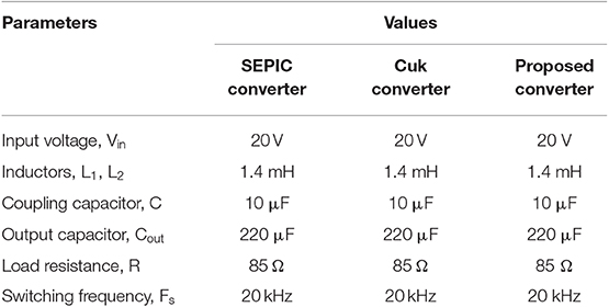
Table 2. Specifications of the proposed SEPIC converter and other converters.
Simulation Study
As per the values presented in Table 2, the converters are designed and simulated using MATLAB/Simulink software. To check the performance of the proposed converter, the traditional converters such as Cuk and SEPIC converter also simulated. For the simplified analysis, the output voltage of the Cuk converter is assumed as a positive voltage; however, the actual output voltage of the Cuk converter is negative. First, the proposed converter is simulated with the duty cycle (D) of 0.6, and the results were depicted in Figure 4.
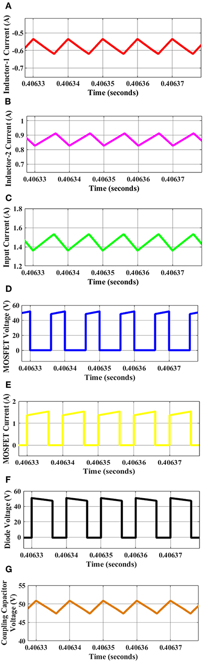
Figure 4. Various simulation waveforms of the proposed converter; (A) Inductor current, iL1, (B) Inductor current, iL2, (C) Input current, Iin, (D) Voltage stress of the MOSFET, (E) Current stress of the MOSFET, (F) Voltage stress of the diode, (G) Voltage across coupling capacitor.
As seen in Figure 4, the proposed converter is operated at CCM operation. As shown in Figures 4A,B, the inductor currents (iL1 and iL2) is oscillating between −0.55 A to −0.62 A, and 0.83 A to 0.91 A, respectively. This result proves that the proposed converter is operated under CCM operation. Another significant advantage of the proposed converter is continuous (constant) input current, and the same can be observed in Figure 4C. The input current is oscillating between 1.38 A and 1.52 A. Thus, the input ripple current of the proposed converter is observed as 0.14 A, which is less than the conventional SEPIC converter, and Cuk converter. Figures 4D,E shows the voltage and current stress of the MOSFET, respectively. The maximum voltage stress of the MOSFET switch is observed as 49.5 V, and the current stress is found as 1.5 A. Figure 4F depicts the voltage stress of the diode, and it is equal to the voltage across the coupling capacitor. Figure 4G illustrates the voltage across the capacitor, and the average voltage is observed as 49 V. Therefore, the diode voltage stress is equal to 49 V as shown in Figure 4F. As per the previous discussion, the proposed converter, and other traditional converters such as SEPIC converter, and Cuk converter also simulated for the duty cycle at 0.6. The load output voltage waveform of all the converters are depicted in Figure 5.
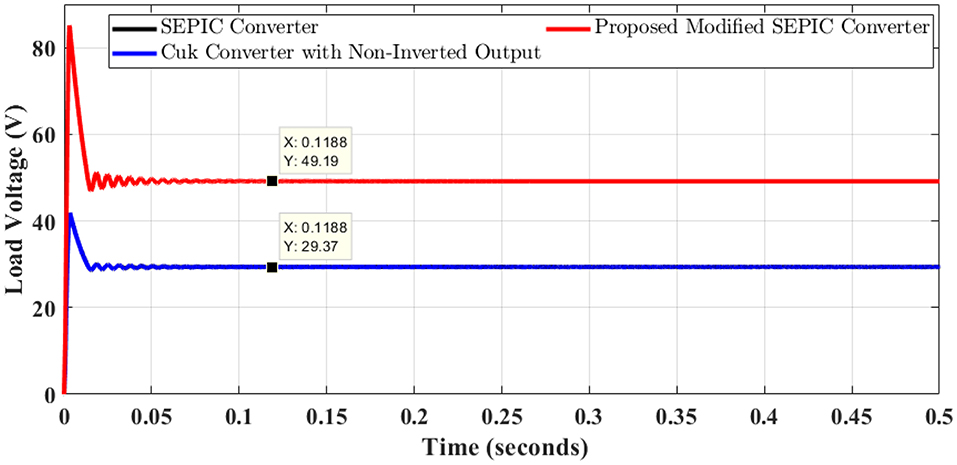
Figure 5. Load output voltage waveform of all the converters at D = 0.6.
The load resistance of all the converter is kept constant at 85 Ω, and the output voltage of the SEPIC converter and Cuk converter is observed as 29.37 V (Cuk converter output voltage is assumed as positive). Whereas, the output load voltage of the proposed modified SEPIC converter is 49.19 V, which is 0.7 times higher than the conventional SEPIC converter. It is also observed that the settling time of all the converters is almost similar. It is concluded that the converter proposed in this paper is having more voltage gain than the traditional SEPIC converter with the same number of components. This high voltage gain is possible only by changing the connections of the conventional SEPIC converter, but not by increasing/decreasing the storage elements or switching devices. The proposed converter is also simulated for different duty cycles, such as 0.4, 0.5, 0.6, and 0.7. The converter switch duty is changed after 0.5 s, duration each. The output load voltage waveform is shown in Figure 6.
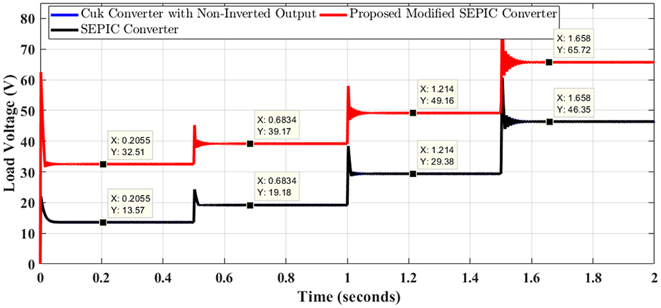
Figure 6. Load output voltage waveform of all the converters at a various duty cycle.
At the start, all the converters are operated with D = 0.4, the output voltage of the SEPIC, Cuk, and proposed converter was observed as 13.57 V, 13.57 V, and 32.51 V, respectively. At t = 0.5 s, the duty cycle is changed to D = 0.5, and the output voltage is witnessed as 19.18 V, 19.18 V, and 39.17 V, respectively. At t = 1 s, the duty cycle is changed to D = 0.6, and the output voltage is observed as 29.38 V, 29.38 V, and 49.16 V, respectively. At t = 1.5 s, the duty cycle is changed to D = 0.7, and the output voltage is observed as 46.35 V, 46.35 V, and 65.72 V, respectively. It is observed and concluded that the duty up to D = 0.5, the SEPIC converter, and the Cuk converter acts as a buck converter, and after D = 0.5, the traditional converters act as a boost converter. Whereas, the proposed converter acts as the boost converter irrespective of the duty cycle as similar to a conventional boost converter with constant input current capability.
Experimental Study
The experimental prototype of the converter is developed and verified in the laboratory environment as per the parameters are shown in Table 2. The experimental prototype is shown in Figure 7. Two inductors of the converter are selected as coupled inductors with EE33 ferrite core. Two strings of twisted copper wire (21 SWG) are wounded on the ferrite core to design the required value of inductance, and twisted pair can minimize the skin effect and coil resistance. The polypropylene metalized film capacitor is selected for a coupling capacitor, which has low ESR (≈ 12.2 mΩ). A low on-state resistance N-Channel MOSFET switch is required for the converter operation, so IRFB4310 MOSFET is selected, which has 5.6 mΩ on-state resistance, and it can withstand up to 100 V, 140 A.
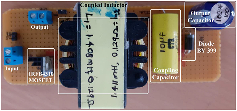
Figure 7. Experimental prototype of the proposed converter.
The converter requires a fast-acting diode to direct the current. Therefore, BY399 fast recovery diode is selected which has less forward voltage drop (<1.1 V) with less reverse recovery time (<500 ns). The PWM pulse is generated using the MSP430FR2355 Texas Instrument development board. A 20 kHz PWM pulse with a 60% duty cycle is given to the MOSFET driver through the optoisolator. The MOSFET switch is driven with 4N25 optoisolator and IR2113 MOSFET driver. The proposed converter prototype is made for 50 W. The proposed converter rating can be extended using multiplier cell circuits if necessary. The adoption of the multiplier circuit is not discussed in this paper. The experimental waveforms are depicted in Figure 8.
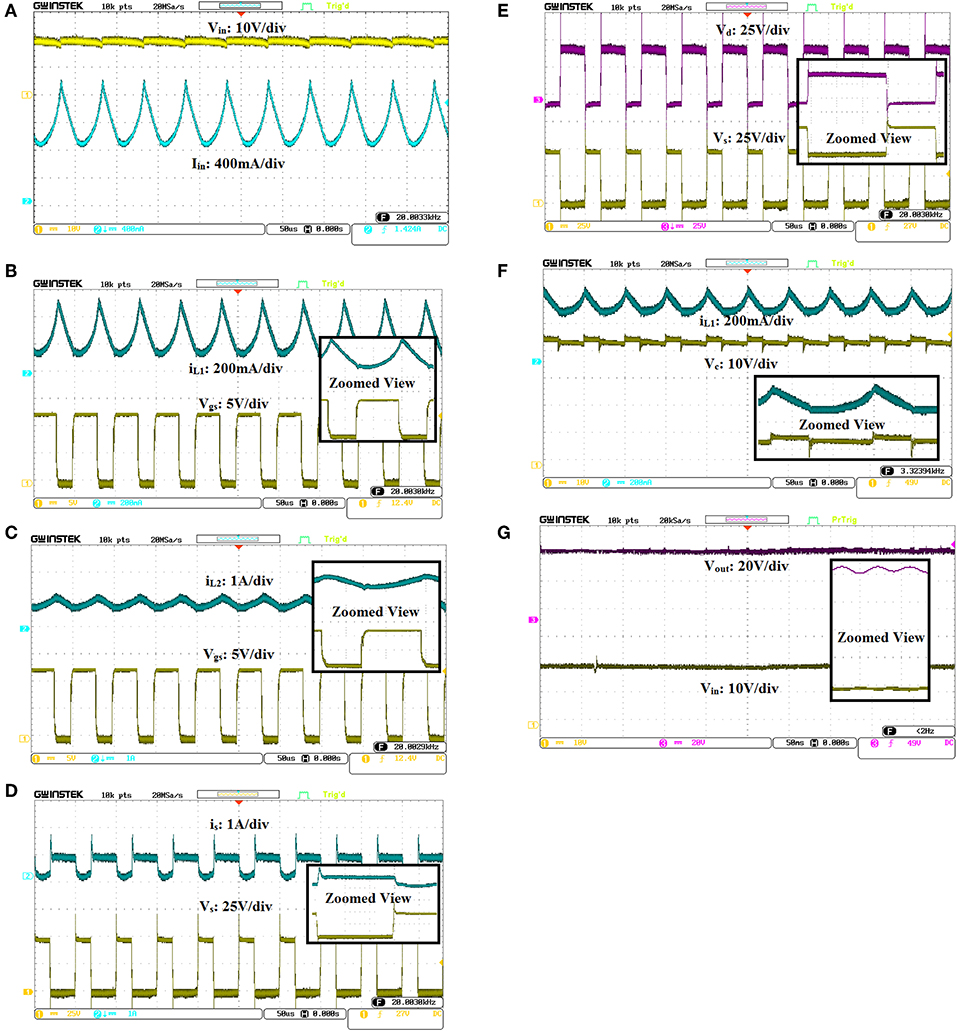
Figure 8. Experimental waveforms of the converter for 60% duty cycle. (A) Input voltage, Vin and input current, Iin; (B) inductor current, iL1 and gate-source voltage, Vgs; (C) inductor current, iL2 and gate-source voltage, Vgs; (D) MOSFET current stress, is and MOSFET voltage stress, Vs; (E) MOSFET voltage stress, Vs and diode voltage stress, Vd; (F) Inductor current, iL1 and voltage across the capacitor, Vc, (G) Input voltage, Vi and output voltage, Vout .
Constant input current is one of the key objectives of this paper, and the same can be seen in Figure 8A. The input current at full load is 1.424 A (average). The input current oscillates between 0.9 A and 1.72 A, and it never reaches zero. The inductor currents such as iL1 and iL2 are depicted in Figures 8B,C, respectively. It is observed from Figures 8B,C, the converter is operated under CCM operation. The peak-peak inductor ripple current as per Equations 20, 21 is selected as 0.43 A. From Figure 8B, the ripple current (ΔiL1) is observed as 0.45 A (oscillation between 0.56 A−0.11 A), and from Figure 8C, the ripple current (ΔiL2) is observed as 0.44 A (oscillation between 0.71 A−1.15 A). This result displays good agreement between the theoretical analysis and the experimental setup. The MOSFET voltage stress and diode can be observed in Figures 8D,E, respectively. As per Equations 13, 14, the maximum voltage stress of the MOSFET switch and the diode is equal to ±Vout. Therefore, the voltage stress of the MOSFET and diode should be equal to 50 V when the duty cycle of the switch is 0.6. The same can be observed clearly in the waveforms as shown in Figures 8D,E. As per Equation 19, the current stress of the MOSFET switch is equal to 0.88 A. From Figure 8D, the current stress is observed as 0.84 A. As per Equation 11, the voltage across the coupling capacitor is equal to the output voltage of the converter which is equal to 50 V. The coupling capacitor voltage observed in Figure 8F is equal to 49 V. Figure 8G depicts the output voltage and the input voltage waveform. As per Equation 12, the output voltage of the converter for the duty cycle, D = 0.6, is equal to 50 V. The converter achieves 49 V experimentally, and this result displays good agreement between the theoretical analysis and the experimental setup. The difference in voltage (≈ 1 V) can be ignored due to the voltage drop in other components. The proposed converter is compared with the other traditional converters in terms of voltage gain and efficiency. Figure 9 shows the performance comparison of the proposed converter.
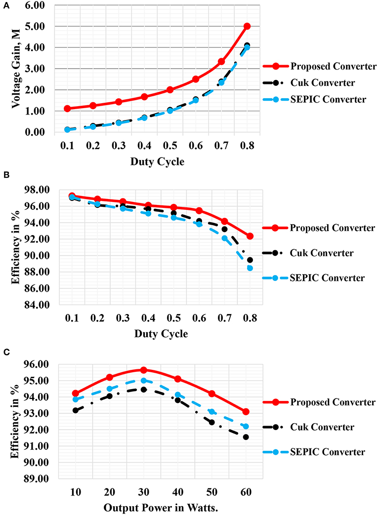
Figure 9. Performance assessment of the proposed converter; (A) Voltage gain for several duty cycles, (B) Efficiency at various duty ratio, (C) Efficiency at different loading conditions.
From the above discussions and the performance comparison presented in Figure 9, it is concluded that the proposed converter is superior in all aspects such as constant input current, high voltage gain, and high conversion efficiency without adding any extra components with the conventional SEPIC converter. The proposed converter is best suited for multi-level boost structure in solar photovoltaic systems or fuel-cell based energy systems instead of the traditional SEPIC converters. Finally, it is concluded that the proposed SEPIC converter can deliver the conversion efficiency at full load condition is equal to 94.2, and 95.64% maximum conversion efficiency.
Conclusion
The converter discussed in this paper improves the voltage conversion ratio than the other traditional dc-dc converters. The proposed SEPIC converter is analyzed in CCM operation, simulated, implemented, and compared with the traditional SEPIC, and Cuk converters. The analysis of various features such as inductor ripple current, voltage conversion, switch and diode voltage stress, and the converter efficiency is made for the proposed converter. The proposed converter is designed based on the theoretical discussions. The results obtained from the simulation, and experimentation is on par with the theoretical discussions. The conversion efficiency of the proposed converter is more than 92% for various duty cycle, and the maximum efficiency is equal to 95.64% at 30 W. This high conversion efficiency makes the proposed converter best suitable for the multilevel boost structure. The converter voltage gain can be further extended by adding the voltage multiplier circuits, and the same will be discussed and developed in future communications. The significant contribution in this paper is that the conventional SEPIC converter is extended without adding any additional equipment, and it behaves like a traditional boost converter with added features as following. (i) high voltage gain, (ii) high conversion efficiency, (iii) continuous input current, and (iv) less output voltage ripple.
Data Availability Statement
The raw data supporting the conclusions of this article will be made available by the authors, without undue reservation, to any qualified researcher.
Author Contributions
Research simulation, experimentation, analysis, revision, and overall layout formation were carried out by MP. Literature review, mathematical analysis, simulation, and proof-read was done by RS. Redesigning the hardware components, experimental testing, revised article, and final proof-read by CK.
Conflict of Interest
The authors declare that the research was conducted in the absence of any commercial or financial relationships that could be construed as a potential conflict of interest.
References
Amir, A., Amir, A., Che, H. S., Elkhateb, A., and Abd Rahim, N. (2019). Comparative analysis of high voltage gain DC-DC converter topologies for photovoltaic systems. Renew. Energy 136, 1147–1163. doi: 10.1016/j.renene.2018.09.089
Ansari, S. A., and Moghani, J. S. (2019). A novel high voltage gain non-coupled inductor SEPIC converter. IEEE Trans. Industr. Electr. 66, 7099–7108. doi: 10.1109/TIE.2018.2878127
Babaei, E., Kangarlu, M. F., Sabahi, M., and Alizadeh-Pahlavani, M. R. (2013). Cascaded multilevel inverter using sub-multilevel cells. Electr. Power Syst. Res. 96, 101–110. doi: 10.1016/j.epsr.2012.10.010
Banaei, M. R., and Bonab, H. A. F. (2016). A novel structure for single-switch non-isolated transformerless buck–boost DC–DC converter. IEEE Trans. Industr. Electr. 64, 198–205. doi: 10.1109/TIE.2016.2608321
Buticchi, G., Costa, L. F., and Liserre, M. (2019). Multi-port DC/DC converter for the electrical power distribution system of the more electric aircraft. Math. Comp. Simul. 158, 387–402. doi: 10.1016/j.matcom.2018.09.019
Chen, S. J., Yang, S. P., Huang, C. M., Chou, H. M., and Shen, M. J. (2018). Interleaved high step-up DC-DC converter based on voltage multiplier cell and voltage-stacking techniques for renewable energy applications. Energies 11:1632. doi: 10.3390/en11071632
Divakar, B. P., Cheng, K. W. E., and Sutanto, D. (2008). Zero-voltage and zero-current switching buck-boost converter with low voltage and current stresses. IET Power Electr. 1, 297–304. doi: 10.1049/iet-pel:20070038
Hegazy, O., Mierlo, J. V., and Lataire, P. (2012). Analysis, modeling, and implementation of a multi-device interleaved DC/DC converter for fuel cell hybrid electric vehicles. IEEE Trans. Power Electr. 27, 4445–4458. doi: 10.1109/TPEL.2012.2183148
Kaouane, M., Boukhelifa, A., and Cheriti, A. (2015). “Regulated output voltage double switch Buck-Boost converter for photovoltaic energy application,” in Proceedings of 3rd International Renewable and Sustainable Energy Conference (Marrakech), 1–6. doi: 10.1109/IRSEC.2015.7455114
Kircioglu, O., Unlu, M., and Çamur, S. (2016). “Modeling and analysis of DC-DC SEPIC converter with coupled inductors,” in Proceedings of International Symposium on Industrial Electronics (Banja Luka), 1–5. doi: 10.1109/INDEL.2016.7797807
Natarajan, S., Padmavathi, P., Kalvakurthi, J. R., Babu, T. S., Ramachandaramurthy, V. K., and Padmanaban, S. (2019). Conducted electromagnetic interference spectral peak mitigation in luo-converter using FPGA-based chaotic PWM technique. Electr. Power Comp. Syst. 47, 838–848. doi: 10.1080/15325008.2019.1629510
Park, K., Moon, G., and Youn, M. (2010). Non-isolated high step-up boost converter integrated with SEPIC converter. IEEE Trans. Power Electr. 25, 2266–2275. doi: 10.1109/TPEL.2010.2046650
Pop-Calimanu, I. M., Lica, S., Popescu, S., Lascu, D., Lie, I., and Mirsu, R. (2019). A new hybrid inductor-based boost DC-DC converter suitable for applications in photovoltaic systems. Energies 12:252. doi: 10.3390/en12020252
Premkumar, M., Karthick, K., and Sowmya, R. (2018a). A comparative study and analysis on conventional solar PV based DC-DC converters and MPPT techniques. Ind. J. Electr. Eng. Comp. Sci. 11, 831–838. doi: 10.11591/ijeecs.v11.i3.pp831-838
Premkumar, M., Sowmya, R., and Karthick, K. (2018b). A dataset of the study on design parameters for the solar photovoltaic charge controller. Data Brief. 21, 1954–1962. doi: 10.1016/j.dib.2018.11.064
Premkumar, M., and Sumithira, T. R. (2019a). Design and implementation of new topology for non-isolated DC-DC microconverter with effective clamping circuit. J. Circuits Syst. Comp. 28:1950082. doi: 10.1142/S0218126619500828
Premkumar, M., and Sumithira, T. R. (2019b). Design and implementation of new topology for solar PV based transformerless forward microinverter. J. Electr. Eng. Technol. 14, 145–155. doi: 10.1007/s42835-018-00036-2
Premkumar, M., Sumithira, T. R., and Sowmya, R. (2018c). Modelling and implementation of cascaded multilevel inverter as solar PV based microinverter using FPGA. Int. J. Intell. Eng. Syst. 11, 18–27. doi: 10.22266/ijies2018.0430.03
Rosas-Caro, J. C., Sanchez, V. M., Valdez-Resendiz, J. E., Mayo-Maldonado, J. C., Beltran-Carbajal, F., and Valderrabano-Gonzalez, A. (2018a). “Quadratic buck-boost converter with positive output-voltage and continuous input-current,” in Proceedings of International Conference on Electronics, Communications and Computers, (Cholula), 152–158. doi: 10.1109/CONIELECOMP.2018.8327191
Rosas-Caro, J. C., Valdez-Resendiz, J. E., Mayo-Maldonado, J. C., Alejo-Reyes, A., and Valderrabano-Gonzalez, A. (2018b). Quadratic buck–boost converter with positive output voltage and minimum ripple point design. IET Power Electr. 11, 1306–1313. doi: 10.1049/iet-pel.2017.0090
Saravanan, S., and Babu, N. R. (2015). “Performance analysis of boost and Cuk converter in MPPT based PV system,” International Conference on Circuits, Power and Computing Technologies (Nagercoil), 1–6. doi: 10.1109/ICCPCT.2015.7159425
Selwan, E., Park, G., and Gajic, Z. (2015). Optimal control of the Cuk converter used in solar cells via a jump parameter technique. IET Control Theory Appl. 9, 893–899. doi: 10.1049/iet-cta.2014.0258
Shamshuddin, M. A., Babu, T. S., Dragicevic, T., Miyatake, M., and Rajasekar, N. (2017). Priority-based energy management technique for integration of solar pv, battery, and fuel cell systems in an autonomous DC microgrid. Electr. Power Comp. Syst. 45, 1881–1891. doi: 10.1080/15325008.2017.1378949
Yousri, D., Babu, T. S., Allam, D., Ramachandaramurthy, V. K., and Etiba, M. B. (2019). A novel chaotic flower pollination algorithm for global maximum power point tracking for photovoltaic system under partial shading conditions. IEEE Access. 7, 121432–121445. doi: 10.1109/ACCESS.2019.2937600
Keywords: boost, CCM, multilevel boost, voltage gain, voltage multiplier, voltage ripple
Citation: Premkumar M, Kumar C and Sowmya R (2019) Analysis and Implementation of High-Performance DC-DC Step-Up Converter for Multilevel Boost Structure. Front. Energy Res. 7:149. doi: 10.3389/fenrg.2019.00149
Received: 04 November 2019; Accepted: 02 December 2019;
Published: 19 December 2019.
Edited by:
Sudhakar Babu Thanikanti, Universiti Tenaga Nasional, MalaysiaReviewed by:
Ravikumar P, KPR Institute of Engineering and Technology, Coimbatore, IndiaKarthik Balasubramanian, Micron Semiconductor Asia Operations Private Limited, Singapore
Copyright © 2019 Premkumar, Kumar and Sowmya. This is an open-access article distributed under the terms of the Creative Commons Attribution License (CC BY). The use, distribution or reproduction in other forums is permitted, provided the original author(s) and the copyright owner(s) are credited and that the original publication in this journal is cited, in accordance with accepted academic practice. No use, distribution or reproduction is permitted which does not comply with these terms.
*Correspondence: M. Premkumar, premkumar.m@gmrit.edu.in