Electronic, Magnetic, and Optical Performances of Non-Metals Doped Silicon Carbide
 Lin Zhang
 Zhen Cui
- 1School of Science, Xi’an University of Technology, Xi’an, China
- 2School of Automation and Information Engineering, Xi’an University of Technology, Xi’an, China
The configurations of nine different non-metals doped silicon carbide (NM-SiC) were structured by using the density functional theory (DFT). The magnetic, electronic, and optical properties of each NM-SiC are investigated at the most stable structure with the maximum binding energy. Although the O-, Si-, and S-SiC systems are still non-magnetic semiconductors, the N- and P-SiC systems have the properties of the magnetic semiconductors. The H-, F-, and Cl-SiC systems exhibit the half-metal behaviors, while the B-SiC system converts to magnetic metal. The redistribution of charges occurs between non-metals atoms and adjacent C atoms. For the same doping position, the more charges are transferred, the greater the binding energy of the NM-SiC system. The work function of the NM-SiC systems is also adjusted by the doping of NM atoms, and achieves the minimum 3.70 eV in the P-SiC, just 77.1% of the original SiC. The absorption spectrum of the NM-SiC systems occurs red-shift in the ultraviolet light region, accompanying the decrease of absorption coefficient. These adjustable magnetic, electronic, and optical performances of NM-SiC expand the application fields of two-dimensional (2D) SiC, especially in designing field emission and spintronics devices.
Introduction
The last few decades, 2D materials (Li and Kaner, 2008; Liu et al., 2014; Zhong et al., 2019; Luo et al., 2021) have been extensively used in optoelectronics (Stankovich et al., 2006; Bratschitsch, 2014; Cui et al., 2021a; Sun et al., 2021), catalysis (Ziletti et al., 2015; Wang et al., 2018), spintronic devices (Komsa et al., 2012; Sun et al., 2017a; Li et al., 2021), energy conversion (Pospischil et al., 2014; Cui et al., 2020a; Sun et al., 2019; Sun and Schwingenschlögl, 2020), and gas sensing (Kooti et al., 2019; Cui et al., 2020b) for their unique structural, optical, electronic and magnetic properties (Eddy and Gaskill, 2009; Castelletto et al., 2014; Yuan et al., 2018; Sun and Schwingenschlögl, 2021). Considering the high thermal capability and carrier mobility of bulk SiC (Mélinon et al., 2007; Susi et al., 2017; Ferdous et al., 2019), the theoretical and experimental research on 2D SiC has aroused significant attention (Hsueh et al., 2011; Chowdhury et al., 2017; Chabi and Kadel, 2020). Although density functional theory predicts that 2D SiC has a graphene-like structure with alternating Si and C atoms (Lambrecht et al., 1993; Bekaroglu et al., 2010), the difficulty in stable 2D SiC synthesis has put the research on a standstill (Lin, 2012). Recently, Chabi et al. (2021) fabricated the stable 2D SiC monolayer by wet exfoliation, and predicted the potential applications in integrated microelectronics circuits and light-emitting devices. This work promotes the enthusiasm for the 2D-SiC and SiC-based systems.
Earlier studies on other 2D materials provide much valuable guidance for the actual application of 2D SiC. Both doping and adsorption are shown to be the effective methods to regulate the 2D material properties (Tang et al., 2018; Cui et al., 2021b). For instance, in transition metal (TM) doping, the orbital hybridization between the TM atom and the substituted atom arouses a robust local magnetization in a 2D material, stimulates the design of spintronics devices (Sun et al., 2017b; Yuan et al., 2020). This potent magnetism has been predicted when the Si or the C atom in SiC system is substitutes by TM atoms, such as, Mn atom (Bezi Javan, 2016; Luo et al., 2017; Wu et al., 2019).
When 2D materials are absorbed or doped by non-metals (NM) atoms, such as, H, N, O, and Cl et al., the orbital hybridization between the NM atom and the substituted atom will not only cause a magnetization in the host 2D material, but also low down the work function which effects the electrons-emitting ability (He et al., 2010; Luo and Shen, 2018). Moreover, the absorption spectrum of 2D material can be tuned to improve the photocatalysis ability by the injection of NM atoms (Cui et al., 2021c). All these predict that NM-SiC systems can be used in spintronics, field emitters, and photocatalysis regions. To the best of our knowledge, the magnetic, electrical, and optical properties of NM-SiC are still unclear. To maximize the 2D-SiC advantage, we investigated the magnetic, electronic, and optical behaviors of nine stable NM doped SiC systematically. Our results show that the properties of these NM-SiC system are changed after the doping of NM atoms. Although the O-, Si-, S-SiC systems are still non-magnetic semiconductors, the N- and P-SiC systems exhibit the properties of the magnetic semiconductors. The H-, F-, and Cl-SiC systems emerge the half-metal behaviors, while the B-SiC is converted to magnetic metal. The work function of the P-SiC is adjusted as low as 3.7 eV, just 77.1% of the 2D-SiC. The red-shift of the absorption spectrum occurs in the ultraviolet light region. These results demonstrate the potential application of NM-SiC in spintronics and field electron-emitting devices.
Computations Details
Vienna Ab Initio Simulation Package was employed to investigate the characteristics of non-metal doped SiC, such as, the band structures, bonding energy, charge transfer, magnetic properties, and work function (Kresse and Furthmüller, 1996). The exchange-related interactions were expressed as the Perdew–Burke–Ernzerhof functions (PBE) based on Generalized gradient approximation (GGA) (Kresse and Joubert, 1999; Perdew et al., 1996). The DFT-D3 of Grimme was used to resolve the weak dispersion forces (Heyd et al., 2003). The cut-off energy of the plane wave was chosen at 550 eV. A 4 × 4×1 NM-SiC supercell substituted by one non-metal atom is structured as depicted in Figure 1A. The Brillouin zone consists of 3 × 3×1 Monkhorst-Pack k-point grids (Grimme et al., 2010). A 15 Å vacuum layer was set in the vertical direction of SiC. All systems are complete relaxed to ensure that the systems reach the most stable states, where the total energy change is lower than 10−5 eV/atom and the Hellmann-Feynman force on each atom is less than 0.01 eV/Å. Then the frequency-dependent dielectric response theory is used to investigate the optical properties of the NM-SiC systems in random-phase approximation (RPA) (Hybertsen and Louie, 1986).
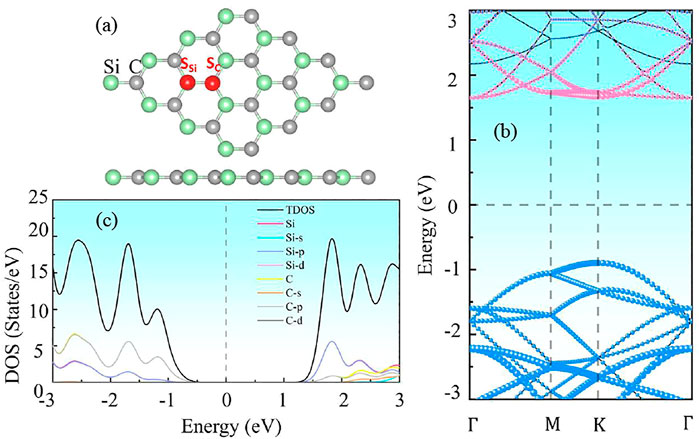
FIGURE 1. The (A) crystal structure, (B) energy band structure, and (C) density of states of intrinsic 2D SiC.
Results and Discussion
The pristine SiC exhibits a complete planar structure, the calculated lattice parameter is 3.10 Å, as shown in Figure 1A. Figure 1B illustrates that 2D SiC is a direct band semiconductor with a gap of 2.52 eV. The density of states (DOS) diagram in Figure 1C demonstrates that the conduction band of SiC is determined by the p orbit of Si, while the valence band is contributed by the p orbit of C primarily. All these results agree with the previous report (Chabi et al., 2021), which confirms the validity of our computational models.
Binding energy is an important parameter reflecting the structural stability of system, and described as follows,
Where Eb is the bonding energy, corresponding to the energy difference of the systems before and after doping. ENM+SiC denotes the energy of the non-metal doped SiC, ESiC represents the energy of the original SiC with one vacancy, ENM is the energy of the doping atom, respectively. The negative binding energy implies that the NM-SiC system has better stability than that before. A larger value indicates a more stable system. The binding energies were calculated at all possible high symmetry doping positions. For 2D SiC, the two possible substituted sites are the SSi (substitute Si atom), and the SC (substitute C atom).
Table 1 lists the parameters of the nine NM-SiC systems with most robust Eb. All the NM-SiC systems present high stability. The steadiest doping position of the NM-SiC systems varies with the doping atoms. The atoms, such as, H, B, N, Si, P, and S, prefer to locate at the position SSi, while the O, F, and Cl atoms select the position SC. For those configurations structured at the position SSi, the B-SiC system exhibits the most potent binding energy. For those configurations at the position SC, the O-SiC system has the largest binding energy. For the same doping position, the stronger the binding energy, the greater the interaction of the NM with the neighboring atoms. The following researches on NM-SiC systems are explored on these steadiest configurations.
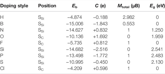
TABLE 1. The doping position, binding energy (Eb), charge transfer (C), band gap (Eg), and magnetic moment (Mtotal) of the NM-SiC systems.
The band structures of the nine different NM-SiC systems are illustrated in Figure 2. It can be seen that the energy band structures of NM-SiC systems are similar to the original SiC system to a large extent. The appearance of the impurity levels causes the change in the SiC band structure. The O-, Si-, and S-SiC are still nonmagnetic semiconductors, and the corresponding band gaps are 1.959 eV (O), 2.541 eV (Si), and 2.130 eV (S), respectively. The H-, B-, N-, F-, P-, and Cl-SiC systems exhibit magnetism for the asymmetry between the spin-up and spin-down components of the energy levels. Among them, the B-SiC is converted to magnetic metal because that Fermi level intersects with both the spin-up and the spin-down components. The H-, F-, and Cl-SiC systems exhibit the half-metal behaviors, and the Fermi level only intersects with the spin-down component. The N- and P-SiC systems convert to magnetic semiconductors with band gaps of 1.250 eV (N) and 2.483 eV (P), respectively.
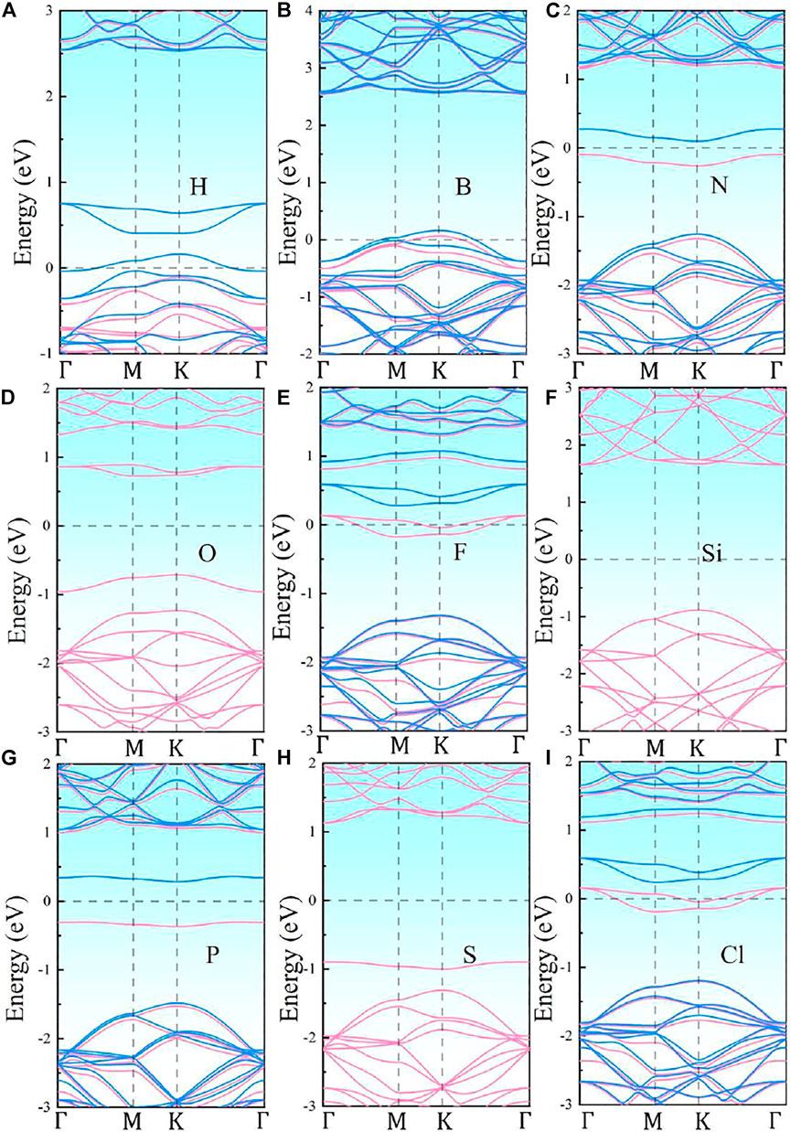
FIGURE 2. The band structures of NM-SiC systems: (A) H-SiC, (B) B-SiC, (C) N-SiC, (D) O-SiC, (E) F-SiC, (F) Si-SiC, (G) P-SiC, (H) S-SiC, (I) Cl-SiC. The pink lines and the blue lines represent the spin-up, and the spin-down components of energy levels, respectively. The Fermi level is shifted to zero.
To analyze the magnetism of NM-SiC systems, the spin-polarized charge density ρ is calculated,
where ρup and ρdown are the up spin-polarized charge density and the down spin-polarized charge density, respectively.
Figure 3 illustrates the spin-polarized charge density distributions of the magnetism H-, B-, N-, F-, P-, and Cl-SiC systems. It can be seen that the spin-polarized charge occurs near the doping atoms and the neighboring atoms. The corresponding magnetism is primarily caused by the doping NM atoms, while the adjacent atoms make a smaller contribution. For metals, the magnetic moment is calculated as 2.982 μB (H), 0.553 μB (B), 1 μB (F), and 1 μB (Cl). When we compare the semiconductor N-,O-, Si, P, and S-SiC systems, it can be seen that the magnetic moment exhibits a regular change with atomic number, 1 μB (N), 0 μB (O), 0 μB (Si), 1 μB (P), and 0 μB (S), respectively. The doping atoms with the same family cause the same magnetic moment, such as, N and P, O and S. This phenomenon can be explained by comparing with the stable non-magnetic SiC. The valence electron difference between the doping atom and the substituted atom are 1 (N), 2 (O), 0 (Si), 1 (P), and 2 (S), respectively. When equal amounts of charge refill the vacancy of the substituted atom, the redundant electrons begin to fill the impurity level with the exclusion principle. And then the corresponding magnetism is formed. This adjustable magnetism expands the application of NM-SiC in nano-spintronics devices.
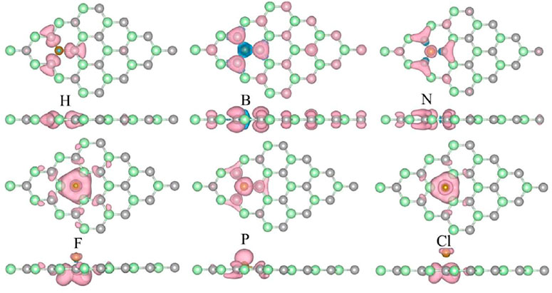
FIGURE 3. The spin-polarized charge density of the metal-doped SiC system. The pink and blue areas represent the contribution of the spin-up, and the spin-down components, respectively. The isovalue is set to 0.001 e/Å3.
The injection of impurity atoms causes the redistribution of charges between the doping and the substituted atoms, which leads to the change in electronic properties of 2D SiC. The charge density difference (CDD) is calculated as follows,
where ρTotal, ρSiC and ρNM represent the charge density of the NM-SiC, the original SiC, and the NM atom, respectively. ∆ρ is the charge density difference of the systems before and after doping. As depicted in Figure 4, the charge transfer occurs between the doping NM atom and the neighboring atoms. The charge transfer is calculated by Bader charges (Henkelman et al., 2006; Sanville et al., 2007), which are, -0.188|e| (H), -1.843|e| (B), +0.832|e| (N), +1.692|e| (O), +0.812|e| (F), −2.516|e| (Si), −1.772|e| (P), -0.450|e| (S), and +0.596|e| (Cl), respectively. The negative sign implies the loss of charge, while the positive sign appears as the obtain of charge. For the N-, O-, F-, and Cl-SiC systems, NM atoms act as acceptors obtaining some charge. For the H-, B-, Si-, P-, and S-SiC systems, NM atoms act as charge donors. A larger Bader charge indicates a more potent charge transfer. For the same doping position, a larger charge transfer indicates a stronger covalent bond interaction between the NM atom and the neighboring atoms (Pino-Rios et al., 2020), corresponding to a more potent binding energy of NM-SiC, as listed in Table 1.
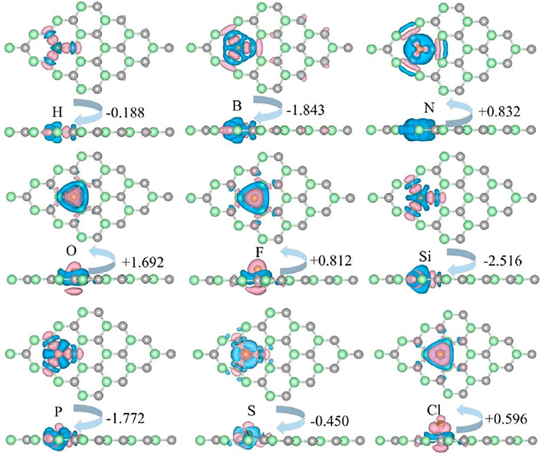
FIGURE 4. The charge density difference of the NM-SiC system. The isovalue is set to 0.001 e/Å3. The pink and the blue regions represent the gain, and the loss of the charge. The negative sign indicates the NM atoms act as charge donors, while the positive sign indicates the NM atoms act as charge acceptors.
As an important electrical parameter of 2D SiC, work function is described as the minimum energy required to make the internal electrons escape into the vacuum. A smaller work function implies a stronger emitting electron capacity. As shown in Figure 5, although the work function of the pristine SiC is 4.82 eV, the work function of NM-SiC systems is regulated between 3.70 and 5.15 eV, covering the range of the traditional field electron emission devices 4.50–5.15 eV (Yu et al., 2009; Jiao et al., 2012; Cai et al., 2014; Soo et al., 2014). The work function of the H- and B-SiC are larger than the pristine SiC, while the N-, O-, F-, P-, S-, and Cl-SiC systems are lower than the pristine SiC. The work function reaches the minimum 3.70 eV in the P-SiC, just 77.1% of the pristine SiC. The NM-SiC systems exhibit the potential in the design of field electron emitter.
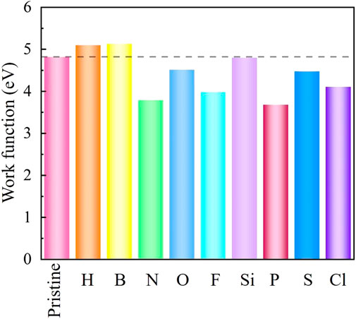
FIGURE 5. The work function of the intrinsic SiC and NM-SiC systems.
Moreover, the changes in the optical absorption spectrum were investigated. As shown in Figure 6, the intrinsic SiC has two acute absorption peaks in the ultraviolet region, and the higher is located at 50.1 nm wavelength with an absorption coefficient of 9.8×105 cm−1. The optical absorption spectrum of NM-SiC varies with the doping atoms. The absorption spectrum occurs red-shift in the ultraviolet light region, and obtains the largest deviation in the P-SiC system.1 The absorption coefficient of NM-SiC experiences a greatly decrease. The absorption properties of NM-SiC systems are adjusted by the doping of the NM atoms.
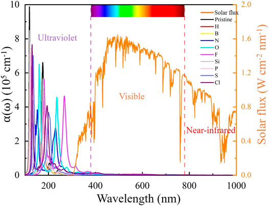
FIGURE 6. The absorption spectrum of intrinsic SiC and NM-SiC systems.
Conclusion
The magnetic, electronic, and optical properties of nine NM-SiC systems were investigated by density functional theory systematically. The steadiest configuration of each NM-SiC system is confirmed at the doping position with the maximum binding energy. Our results show that the optimal doping position varies with the NM atoms. The atoms H, B, N, Si, P, and S prefer to locate at the position SSi, while the O, F, and Cl select the position SC. The doping of the NM atoms causes the change in the properties of SiC system. Although the O-, S-, and Si-SiC systems are still non-magnetic semiconductors, the N- and P-SiC systems have the properties of the magnetic semiconductors. The H-, F-, and Cl-SiC systems exhibit the half-metal behaviors, while the B-SiC system converts to magnetic metal. The charges transfer between the NM atoms and the adjacent C atoms. For the same doping position, a more significant charge transfer indicates stronger binding energy of NM-SiC. The redistribution of charge causes the change in the work function of NM-SiC. In the N-, O-, F-, P-, S-, and Cl-SiC systems, the work function exhibits a decrease, and it achieves the minimum 3.70 eV in the P-SiC, just 77.1% of the pristine SiC. Compared with the pristine SiC, the absorption peaks intensity of each NM-SiC is decreased. The absorption spectrum occurs red-shift in the ultraviolet light region. All these results indicate the possibility of tuning the electronic, magnetic performance of NM-SiC by the doping of suitable non-metal atoms. This study provides theoretical guidance for designing 2D SiC-based spintronics and field emission devices.
Data Availability Statement
The original contributions presented in the study are included in the article/Supplementary Material, further inquiries can be directed to the corresponding author.
Author Contributions
LZ: Conceptualization, methodology, writing–review and editing. ZC: Supervision, writing–review and editing.
Conflict of Interest
The authors declare that the research was conducted in the absence of any commercial or financial relationships that could be construed as a potential conflict of interest.
Publisher’s Note
All claims expressed in this article are solely those of the authors and do not necessarily represent those of their affiliated organizations or those of the publisher, the editors, and the reviewers. Any product that may be evaluated in this article, or claim that may be made by its manufacturer, is not guaranteed or endorsed by the publisher.
Acknowledgments
The authors thanks the National Natural Science Foundation of China (Grant No. 11904285).
Footnotes
1The AM 1.5G spectrum was taken from the NREL website, http://rredc.nrel.gov/solar/spectra/am.1.5.
References
Bekaroglu, E., Topsakal, M., Cahangirov, S., and Ciraci, S. (2010). First-principles Study of Defects and Adatoms in Silicon Carbide Honeycomb Structures. Phys. Rev. B, Condens. Matter Mater. Phys. 81, 1–9. doi:10.1103/physrevb.81.075433
Bezi Javan, M. (2016). Electronic and Magnetic Properties of Monolayer SiC Sheet Doped with 3d-Transition Metals. J. Magnetism Magn. Mater. 401, 656–661. doi:10.1016/j.jmmm.2015.10.103
Bratschitsch, R. (2014). Monolayer Diodes Light up. Nat. Nanotech 9, 247–248. doi:10.1038/nnano.2014.66
Cai, Y., Zhang, G., and Zhang, Y.-W. (2014). Layer-dependent Band Alignment and Work Function of Few-Layer Phosphorene. Sci. Rep. 4, 6677. doi:10.1038/srep06677
Castelletto, S., Johnson, B. C., Ivády, V., Stavrias, N., Umeda, T., Gali, A., et al. (2014). A Silicon Carbide Room-Temperature Single-Photon Source. Nat. Mater 13, 151–156. doi:10.1038/nmat3806
Chabi, S., Guler, Z., Brearley, A. J., Benavidez, A. D., and Luk, T. S. (2021). The Creation of True Two-Dimensional Silicon Carbide. Nanomaterials 11, 1799. doi:10.3390/nano11071799
Chabi, S., and Kadel, K. (2020). Two-dimensional Silicon Carbide: Emerging Direct Band gap Semiconductor. Nanomaterials 10, 2226. doi:10.3390/nano10112226
Chowdhury, C., Karmakar, S., and Datta, A. (2017). Monolayer Group IV-VI Monochalcogenides: Low-Dimensional Materials for Photocatalytic Water Splitting. J. Phys. Chem. C 121, 7615–7624. doi:10.1021/acs.jpcc.6b12080
Cui, Z., Bai, K., Ding, Y., Wang, X., Li, E., Zheng, J., et al. (2020). Electronic and Optical Properties of Janus MoSSe and ZnO vdWs Heterostructures. Superlattices and Microstructures 140, 106445. doi:10.1016/j.spmi.2020.106445
Cui, Z., Luo, Y., Yu, J., and Xu, Y. (2021). Tuning the Electronic Properties of MoSi2N4 by Molecular Doping: A First Principles Investigation. Physica E: Low-dimensional Syst. Nanostructures 134, 114873. doi:10.1016/j.physe.2021.114873
Cui, Z., Lyu, N., Ding, Y., Bai, K., and Bai, K. F. (2021). Noncovalently Functionalization of Janus MoSSe Monolayer with Organic Molecules. Physica E: Low-dimensional Syst. Nanostructures 127, 114503. doi:10.1016/j.physe.2020.114503
Cui, Z., Wang, M., Lyu, N., Zhang, S., Ding, Y., and Bai, K. (2021). Electronic, Magnetism and Optical Properties of Transition Metals Adsorbed Puckered Arsenene. Superlattices and Microstructures 152, 106852. doi:10.1016/j.spmi.2021.106852
Cui, Z., Wang, X., Ding, Y., Li, E., Bai, K., Zheng, J., et al. (2020). Adsorption of CO, NH3, NO, and NO2 on Pristine and Defective g-GaN: Improved Gas Sensing and Functionalization. Appl. Surf. Sci. 530, 147275. doi:10.1016/j.apsusc.2020.147275
Eddy, C. R., and Gaskill, D. K. (2009). Silicon Carbide as a Platform for Power Electronics. Science 324, 1398–1400. doi:10.1126/science.1168704
Ferdous, N., Islam, S., Park, J., and Hashimoto, A. (2019). Tunable Electronic Properties in Stanene and Two Dimensional Silicon-Carbide Heterobilayer: A First Principles Investigation. AIP Adv. 9, 025120. doi:10.1063/1.5066029
Grimme, S., Antony, J., Ehrlich, S., and Krieg, H. (2010). A Consistent and Accurate Ab Initio Parametrization of Density Functional Dispersion Correction (DFT-D) for the 94 Elements H-Pu. J. Chem. Phys. 132, 154104. doi:10.1063/1.3382344
He, J., Wu, K., Sa, R., Li, Q., and Wei, Y. (2010). Magnetic Properties of Nonmetal Atoms Absorbed MoS2 Monolayers. Appl. Phys. Lett. 96, 082504. doi:10.1063/1.3318254
Henkelman, G., Arnaldsson, A., and Jónsson, H. (2006). A Fast and Robust Algorithm for Bader Decomposition of Charge Density. Comput. Mater. Sci. 36, 354–360. doi:10.1016/j.commatsci.2005.04.010
Heyd, J., Scuseria, G. E., and Ernzerhof, M. (2003). Hybrid Functionals Based on a Screened Coulomb Potential. J. Chem. Phys. 118, 8207–8215. doi:10.1063/1.1564060
Hsueh, H. C., Guo, G. Y., and Louie, S. G. (2011). Excitonic Effects in the Optical Properties of a SiC Sheet and Nanotubes. Phys. Rev. B 84, 085404. doi:10.1103/physrevb.84.085404
Hybertsen, M. S., and Louie, S. G. (1986). Electron Correlation in Semiconductors and Insulators: Band Gaps and Quasiparticle Energies. Phys. Rev. B 34, 5390–5413. doi:10.1103/physrevb.34.5390
Jiao, N., He, C., Zhang, C. X., Peng, X., Zhang, K. W., and Sun, L. Z. (2012). Modulation Effect of Hydrogen and Fluorine Decoration on the Surface Work Function of BN Sheets. AIP Adv. 2, 022125. doi:10.1063/1.4719097
Komsa, H. P., Kotakoski, J., Kurasch, S., Lehtinen, O., Kaiser, U., and Krasheninnikov, A. V. (2012). Two-dimensional Transition Metal Dichalcogenides under Electron Irradiation: Defect Production and Doping. Phys. Rev. Lett. 109, 035503. doi:10.1103/PhysRevLett.109.035503
Kooti, M., Keshtkar, S., Askarieh, M., and Rashidi, A. (2019). Progress toward a Novel Methane Gas Sensor Based on SnO2 Nanorods-Nanoporous Graphene Hybrid. Sensors Actuators B: Chem. 281, 96–106. doi:10.1016/j.snb.2018.10.032
Kresse, G., and Furthmüller, J. (1996). Efficient Iterative Schemes Forab Initiototal-Energy Calculations Using a Plane-Wave Basis Set. Phys. Rev. B 54, 11169–11186. doi:10.1103/physrevb.54.11169
Kresse, G., and Joubert, D. (1999). From Ultrasoft Pseudopotentials to the Projector Augmented-Wave Method. Phys. Rev. B 59, 1758–1775. doi:10.1103/physrevb.59.1758
Lambrecht, W. R. L., Segall, B., Suttrop, W., Yoganathan, M., Devaty, R. P., Choyke, W. J., et al. (1993). Optical Reflectivity of 3C and 4H‐SiC Polytypes: Theory and experiment. Appl. Phys. Lett. 63, 2747–2749. doi:10.1063/1.110322
Li, D., and Kaner, R. B. (2008). Graphene-based Materials. Science 320, 1170–1171. doi:10.1126/science.1158180
Li, D., Li, S., Zhong, C., and He, J. (2021). Tuning Magnetism at the Two-Dimensional Limit: a Theoretical Perspective. Nanoscale 13, 19812–19827. doi:10.1039/d1nr06835k
Lin, S. S. (2012). Light-emitting Two-Dimensional Ultrathin Silicon Carbide. J. Phys. Chem. C 116, 3951–3955. doi:10.1021/jp210536m
Liu, H., Neal, A. T., Zhu, Z., Luo, Z., Xu, X., Tománek, D., et al. (2014). Phosphorene: an Unexplored 2D Semiconductor with a High Hole Mobility. ACS Nano 8, 4033–4041. doi:10.1021/nn501226z
Luo, M., and Shen, Y. H. (2018). Magnetic Properties of SiC Monolayer with Different Nonmagnetic Metal Dopants. J. Supercond. Nov. Magn. 31, 3277–3282. doi:10.1007/s10948-018-4589-8
Luo, M., Shen, Y. H., and Yin, T. L. (2017). Ab Initio study of Electronic and Magnetic Properties in TM-Doped 2D Silicon Carbide. Physica E: Low-dimensional Syst. Nanostructures 85, 280–284. doi:10.1016/j.physe.2016.08.028
Luo, Y., Ren, C., Xu, Y., Yu, J., Wang, S., and Sun, M. (2021). A First Principles Investigation on the Structural, Mechanical, Electronic, and Catalytic Properties of Biphenylene. Sci. Rep. 11, 19008. doi:10.1038/s41598-021-98261-9
Mélinon, B., Masenelli, F., and Tournus, A. (2007). Perez, Playing with Carbon and Silicon at the Nanoscale. Nat. Mater. 6, 479–490. doi:10.1016/j.nanoen.2018.07.041
Perdew, J. P., Burke, K., and Ernzerhof, M. (1996). Generalized Gradient Approximation Made Simple. Phys. Rev. Lett. 77, 3865–3868. doi:10.1103/physrevlett.77.3865
Pino-Rios, R., Chigo-Anota, E., Shakerzadeh, E., and Cárdenas-Jirón, G. (2020). B12N12 Cluster as a Collector of noble Gases: A Quantum Chemical Study. Physica E: Low-dimensional Syst. Nanostructures 115, 113697. doi:10.1016/j.physe.2019.113697
Pospischil, A., Furchi, M. M., and Mueller, T. (2014). Solar-energy Conversion and Light Emission in an Atomic Monolayer P-N Diode. Nat. Nanotech 9, 257–261. doi:10.1038/nnano.2014.14
Sanville, E., Kenny, S. D., Smith, R., and Henkelman, G. (2007). Improved Grid-Based Algorithm for Bader Charge Allocation. J. Comput. Chem. 28, 899–908. doi:10.1002/jcc.20575
Soo, H. C., Zhang, S. L., and Woo, C. Y. (2014). Layer-number-dependent Work Function of MoS2 Nanoflakes. J. Kor. Phys. Soc. 64, 1550–1555.
Stankovich, S., Dikin, D. A., Dommett, G. H. B., Kohlhaas, K. M., Zimney, E. J., Stach, E. A., et al. (2006). Graphene-based Composite Materials. Nature 442, 282–286. doi:10.1038/nature04969
Sun, M., Chou, J.-P., Ren, Q., Zhao, Y., Yu, J., and Tang, W. (2017). Tunable Schottky barrier in van der Waals heterostructures of graphene and g-GaN. Appl. Phys. Lett. 110, 173105. doi:10.1063/1.4982690
Sun, M. L., and Schwingenschlögl, U. (2020). A Direct-Band-gap Semiconductor Combining Auxeticity, Ferroelasticity, and Potential for High-Efficiency Solar Cells. Phys. Rev. Appl. 14, 044015. doi:10.1103/physrevapplied.14.044015
Sun, M., Luo, Y., Yan, Y., and Schwingenschlögl, U. (2021). Ultrahigh Carrier Mobility in the Two-Dimensional Semiconductors B8Si4, B8Ge4, and B8Sn4. Chem. Mater. 33, 6475–6483. doi:10.1021/acs.chemmater.1c01824
Sun, M., Ren, Q., Zhao, Y., Chou, J.-P., Yu, J., and Tang, W. (2017). Electronic and Magnetic Properties of 4d Series Transition Metal Substituted Graphene: a First-Principles Study. Carbon 120, 265–273. doi:10.1016/j.carbon.2017.04.060
Sun, M., and Schwingenschlögl, U. (2021). Unique Omnidirectional Negative Poisson's Ratio in δ-Phase Carbon Monochalcogenides. J. Phys. Chem. C 125, 4133–4138. doi:10.1021/acs.jpcc.0c11555
Sun, S., Hussain, T., Zhang, W., and Karton, A. (2019). Blue Phosphorene Monolayers as Potential Nano Sensors for Volatile Organic Compounds under point Defects. Appl. Surf. Sci. 486, 52–57. doi:10.1016/j.apsusc.2019.04.223
Susi, T., Skákalová, V., Mittelberger, A., Kotrusz, P., Hulman, M., Pennycook, T. J., et al. (2017). Computational Insights and the Observation of SiC Nanograin Assembly: Towards 2D Silicon Carbide. Sci. Rep. 7, 4399–9. doi:10.1038/s41598-017-04683-9
Tang, W., Sun, M., Yu, J., and Chou, J.-P. (2018). Magnetism in Non-metal Atoms Adsorbed Graphene-like Gallium Nitride Monolayers. Appl. Surf. Sci. 427, 609–612. doi:10.1016/j.apsusc.2017.08.210
Wang, S., Ren, C., Tian, H., Yu, J., and Sun, M. (2018). MoS2/ZnO van der Waals heterostructure as a high-efficiency water splitting photocatalyst: a first-principles study. Phys. Chem. Chem. Phys. 20, 13394–13399. doi:10.1039/c8cp00808f
Wu, C.-W., Huang, J.-H., and Yao, D.-X. (2019). Tunable Room-Temperature Ferromagnetism in the SiC Monolayer. J. Magnetism Magn. Mater. 469, 306–314. doi:10.1016/j.jmmm.2018.08.054
Yu, Y.-J., Zhao, Y., Ryu, S., Brus, L. E., Kim, K. S., and Kim, P. (2009). Tuning the Graphene Work Function by Electric Field Effect. Nano Lett. 9, 3430–3434. doi:10.1021/nl901572a
Yuan, J., Cai, Y., Shen, L., Xiao, Y., Ren, J.-C., Wang, A., et al. (2018). One-dimensional Thermoelectrics Induced by Rashba Spin-Orbit Coupling in Two-Dimensional BiSb Monolayer. Nano energy 52, 163–170.
Yuan, J., Chen, Y., Xie, Y., Zhang, X., Rao, D., Guo, Y., et al. (2020). Squeezed Metallic Droplet with Tunable Kubo gap and Charge Injection in Transition Metal Dichalcogenides. Proc. Natl. Acad. Sci. U.S.A. 117, 6362–6369. doi:10.1073/pnas.1920036117
Zhong, C., Wu, W., He, J., Ding, G., Liu, Y., Li, D., et al. (2019). Two-dimensional Honeycomb Borophene Oxide: strong Anisotropy and Nodal Loop Transformation. Nanoscale 11, 2468–2475. doi:10.1039/c8nr08729f
Keywords: silicon carbide, magnetism, non-metals, electronic and optical properties, work function (WF)
Citation: Zhang L and Cui Z (2022) Electronic, Magnetic, and Optical Performances of Non-Metals Doped Silicon Carbide. Front. Chem. 10:898174. doi: 10.3389/fchem.2022.898174
Received: 17 March 2022; Accepted: 31 March 2022;
Published: 19 April 2022.
Edited by:
Minglei Sun, King Abdullah University of Science and Technology, Saudi ArabiaCopyright © 2022 Zhang and Cui. This is an open-access article distributed under the terms of the Creative Commons Attribution License (CC BY). The use, distribution or reproduction in other forums is permitted, provided the original author(s) and the copyright owner(s) are credited and that the original publication in this journal is cited, in accordance with accepted academic practice. No use, distribution or reproduction is permitted which does not comply with these terms.
*Correspondence: Zhen Cui, zcui@xaut.edu.cn