1. Introduction
In recent years, the scanning acoustic microscopy (SAM) system has been widely used in the field of nondestructive testing to detect defects such as voids inside rigid structures [
1,
2,
3,
4]. The SAM system uses high-frequency ultrasonic signals to restore images of the internal structure of the object under examination [
5,
6]. A high-frequency ultrasound (>20 MHz) allows small structures to be captured because of its good spatial resolution in the order of tens of micrometers. The SAM system has been used in many different fields, in which succession must be followed. Burak Altun et al. used the SAM system to analyze the impedance measurement of tissue. Their research plays an important role in ensuring the quality of ultrasound diagnostics [
7]. Ryo Nagaoka et al. have developed a new calculation method for the SAM system to measure objects with a thickness of 1.95 um with an accuracy of 0.0016% [
2]. C. Uhrenfeldt et al. adopted SAM to evaluate power electronic components with a nondestructive testing (NDT) method [
8]. L. Pitta Bauremann et al. used SAM to identify battery defects [
9]. M. Hertl et al. used SAM to scan interior images of electronic components [
10]. The complete SAM system includes five main parts: a transducer, a pulser/receiver, a digitizer, a motion controller and image processing [
1]. For high-frequency transducers with small focal zones, small dimensions can be detected in the structure to be tested [
10]. Therefore, the ultrasonic transducer strategy, which converts electrical energy into high-frequency sound waves, is an important consideration for optimizing system performance and achieving high image quality [
2,
7].
There have been many studies on how to generate a signal to the excitation transducer [
11]. These studies mainly focused on generating arbitrary waveforms to the excitation transducer to increase the signal-to-noise ratio (SNR) and increase the resolution of the resulting images [
11,
12,
13,
14,
15]. However, these studies have not focused on deploying a complete device for nondestructive testing (NDT) and SAM systems. In this study, we will discuss the complete pulser/receiver (P/R) device used in the SAM system and the methods for increasing the scanning speed of the SAM system [
12,
16,
17,
18,
19,
20].
There are usually two types of pulses used to excite transducers: unipolar and bipolar pulses [
2,
21,
22]. The bipolar pulses carry a high amount of energy, but the bandwidth is small [
23,
24]. The bipolar pulse is often used with applications that use low-frequency transducers [
2,
7,
9,
25]. Unipolar pulses with higher bandwidths bring smaller power, suitable for applications using high-frequency transducers. Therefore, unipolar pulses can produce a vertical resolution (interlayer resolution) better than that of bipolar pulses [
9,
26]. In this study, we will present the design of a unipolar P/R device to stimulate the transducer for imaging applications [
27]. The programed P/R is fully compatible with SAM systems and many transducers with different operating frequencies. Typically, traditional SAM systems use one transducer, but our P/R equipment is designed to be used simultaneously with four transducers. Thus, the scanning speed of the new SAM system is four times that of a traditional SAM system.
One of the most critical problems of P/R devices is the generation of unipolar pulses with high voltages and small duty cycles (<10 ns) [
8]. There are two steps to creating this pulse. The first step is using a field programmable gate array (FPGA) to generate pulses with small duty cycles and low voltage amplitudes. The second step is using this pulse to excite a high-frequency Metal-Oxide Semiconductor Field-Effect Transistor (MOSFET) in order to generate high voltage signals that trigger the transducer [
26]. However, this pulse is very difficult to perform and is often directly affected by elements on the printed circuit board (PCB). High frequency signals on the PCB often include overshooting and undershooting parts. Therefore, the design of the PCB and P/R equipment should be optimized to achieve the best signal [
28,
29].
This paper makes two main contributions. We presented the structure and components of a complete P/R device with high flexibility that can easily be integrated into many SAM systems with different transducer types. Secondly, we presented a technique for using damping resistors to optimize unipolar pulses in order to excite high-frequency transducers, achieving a high signal-to-noise ratio. The PCB design for these signal lines is also presented in detail. The P/R device design has four channels, which makes it easy to deploy a SAM system with four transducers to reduce the scan time of a sample. This is one of the highlights when compared with similar products like the UT320 (UTEX Scientific Instruments Inc., Mississauga, ON, Canada) [
30] (only one channel) or the DPR500 (Imaginant Inc., Pittsford, NY, USA) [
22] (two channels). On the other hand, the P/R device can be expanded with eight channels.
The rest of this paper is organized as follows.
Section 2 is a description of the completed design of the P/R device. The implementation of the hardware and code is introduced in
Section 3. The detailed setup for testing and the results are presented in
Section 4. Finally, a concluding remark is given in
Section 5.
2. Materials and Methods
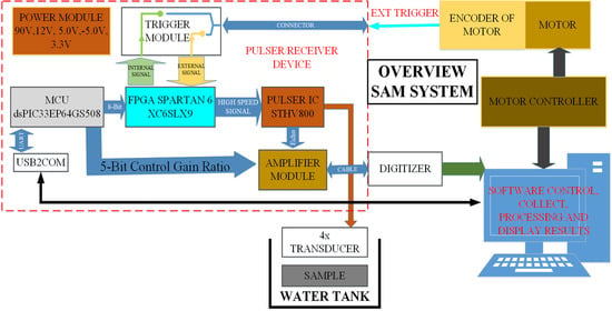
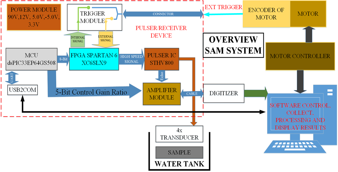
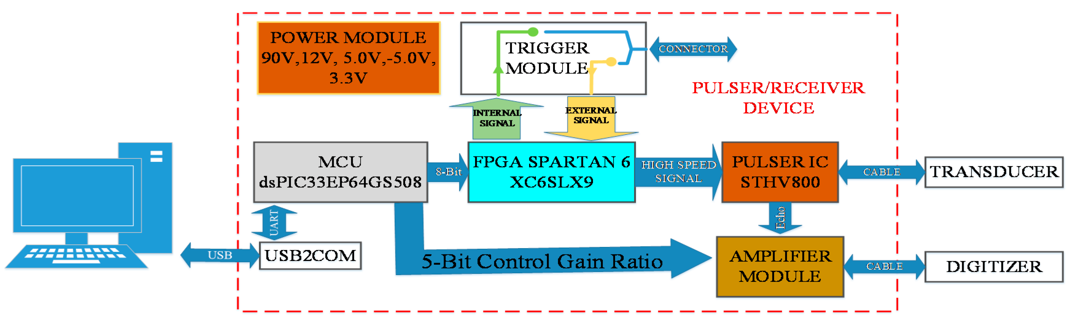
A description of the main modules of the P/R device is presented in
Figure 1. The FPGA (XC6LSX9-2TQG144C, Premier Farnell, Leeds, UK) [
31] and Pulser STHV800 (LIFE.AUGMENTED., Monza, Italy) [
32] chips were responsible for generating unipolar pulses to excite the high-frequency transducers. The PCB for this design required advanced technology of a high quality. The dsPIC33EP64GS508 [
33] chip was responsible for communicating with the PC via the USB2COM (TITAN Electronics Inc., Chicago, IL, USA) interface, both to receive commands from the PC and to control the FPGA chip through 8-bit communication. Besides that, the dsPIC33EP64GS508 chip also selected the gain of the amplifier module. The trigger module was responsible for synchronizing signals with external signal sources or connecting to the motor encoder in the SAM system. We proposed a complete P/R device, which is shown in
Figure 1.
2.1. Configuration Software
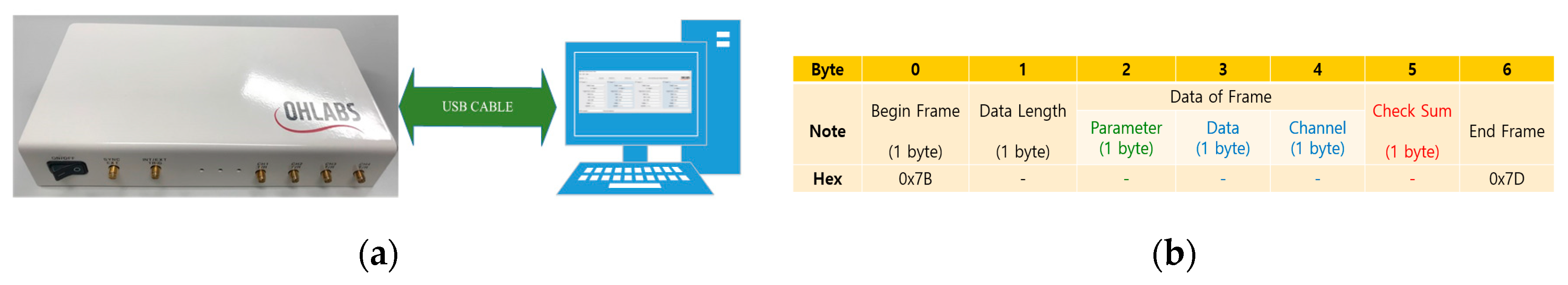
Figure 2a describes the interface software for configuring the P/R parameters. The communication protocol between the P/R device and the software is described in
Figure 2b. This is a fairly simple protocol which is used in a number of devices of the same type. The software was implemented based on Qt Creator 4.9 and compiled in C ++.
Table 1 describes the functions of the configurational software for each channel of the P/R device.
2.2. Hardware Design
Hardware design was one of the most important parts of our research. The hardware was implemented with Altinum Designer v.19 (Altium, San Diego, CA, USA) and was divided into two parts: schematic design and PCB layout. In this hardware design, we focused on a high-speed design for signal communication between the FPGA chip and the STHV800 chip, as well as the analog signal received from the transducer to be entered into the digitizer device. Besides that, the PCB layout is presented in detail for each module, including the designs of the pulser/receiver module, trigger module, and amplifier module.
2.3. Solution for Design the Pulser/Receiver Module
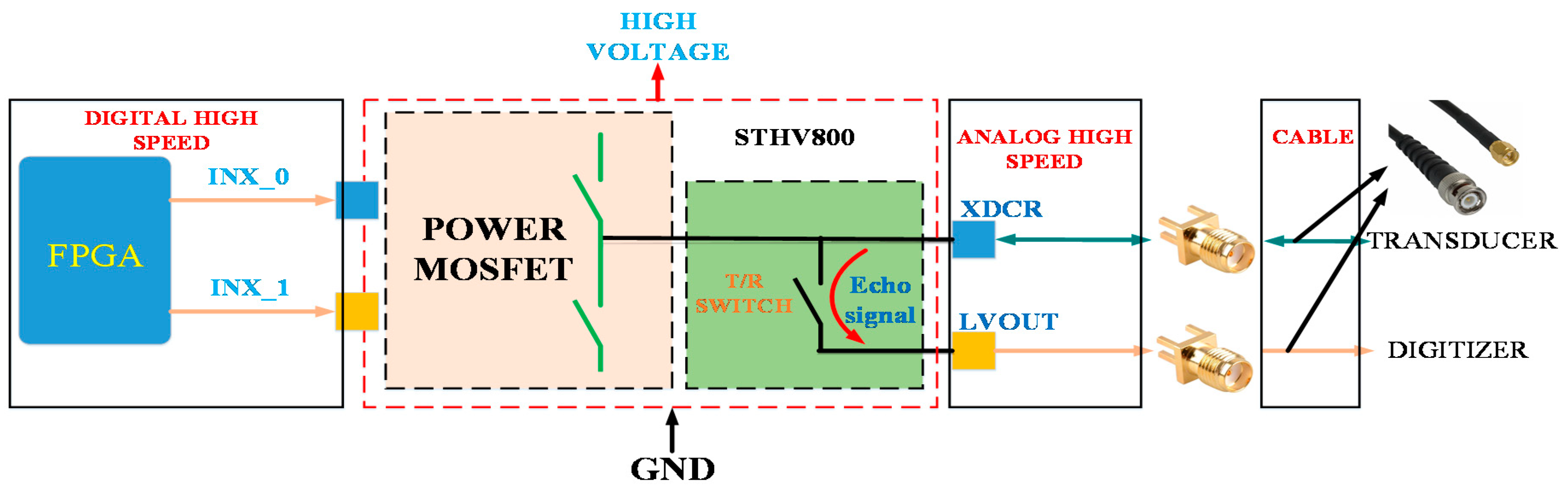
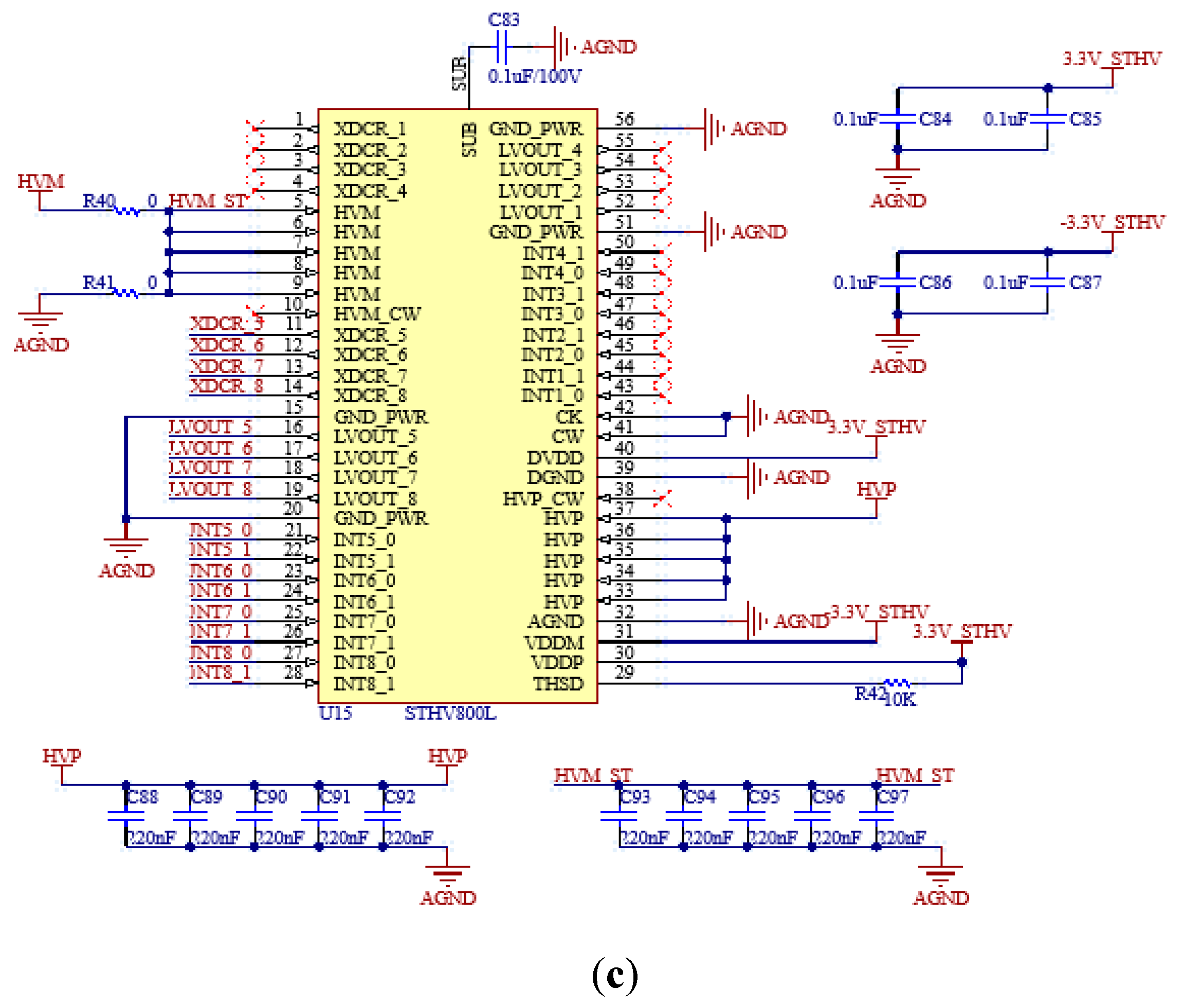
The STHV800 had eight independent channels. The device comprised the controller logic interface circuit, level translator, MOSFET driver, noise-blocking diodes, and high-power P and N channel MOSFETs as the output stage for each channel. The main issues during the PCB design process were achieving capacitance values that ensured good filtering and effective separation between the low voltage inputs and high voltage switching signals.
Figure 3 describes the hardware design to control a channel of the STHV800. Controlling a channel required two control signals from the FPGA, both of which required a high-speed circuit design (the duty part of the signal will determine the bandwidth of the P/R device). Besides that, the signal from the pin name XDCR was directly connected to the transducer to trigger the transducer with high voltage, then also receive an echo signal from the transducer. The signal from the pin name LVOUT was connected to the digitizer to analyze the transducer’s echo signal. The signal from the XDCR and LVOUT pins was designed to meet the high-speed analog signals [
32].
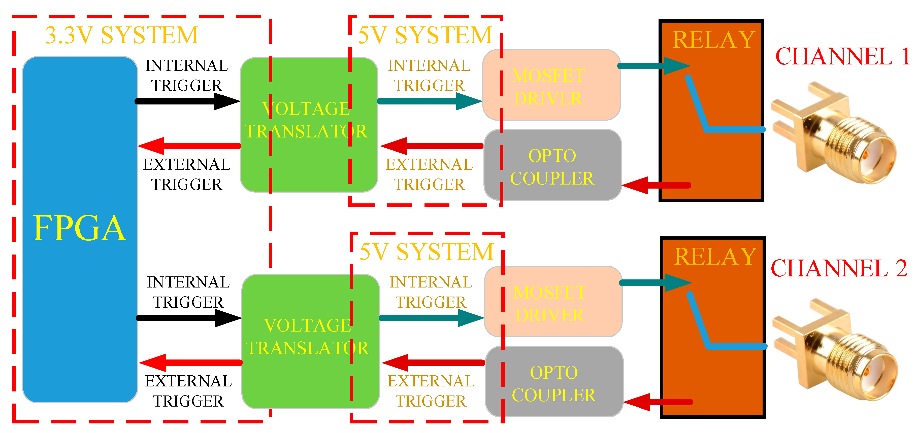
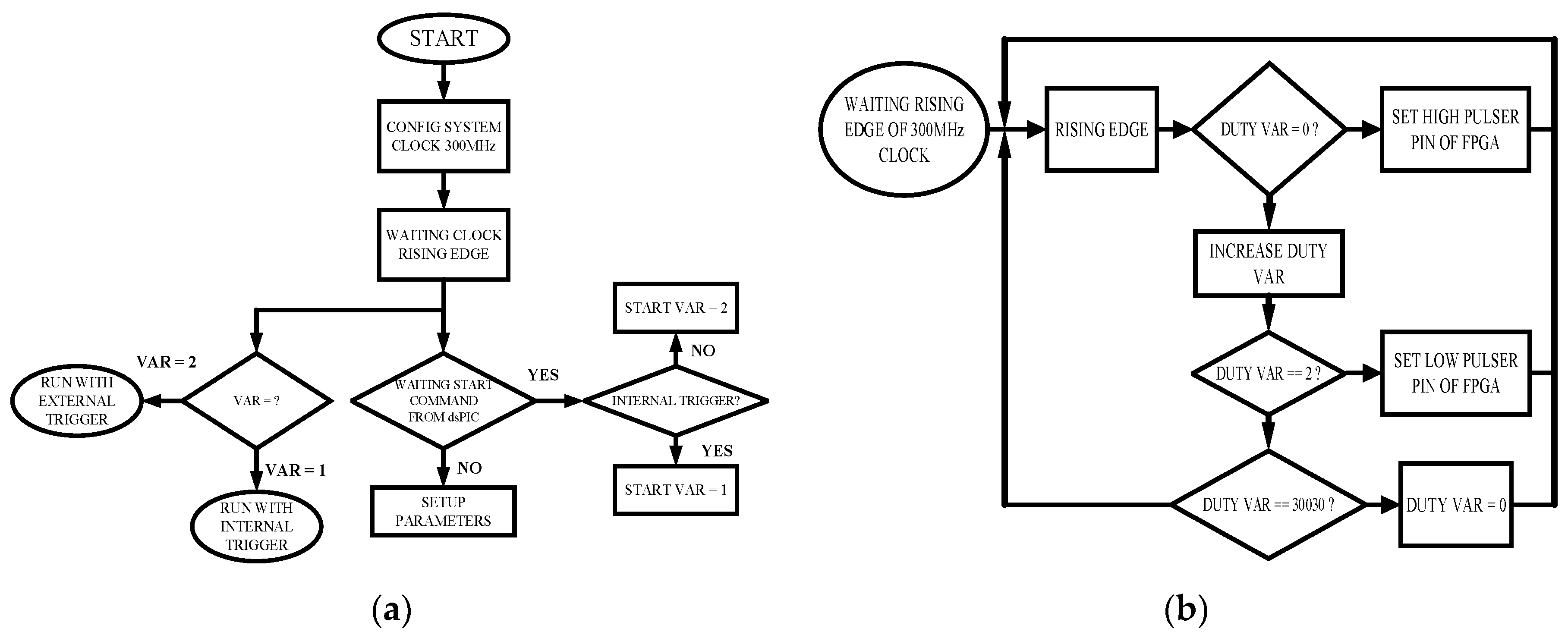
2.4. Solution for Design the Trigger Module
The trigger module was capable of generating a square pulse signal with a frequency from 100 Hz to 50 kHz and receiving another square pulse signal with a frequency of up to 100 kHz. The trigger is an important module, significant in determining the transducer’s focus point (internal trigger). The external trigger module could receive signals from the motor encoder and then create another trigger signal for the pulser and the digitizer, beginning the data receiving cycle. The operation of this module is described in
Figure 4.
Our design consisted of two of the same trigger channels, but they could work independently of each other. The connection of the trigger signal to the excitation channel of the STHV800 chip was configured using software.
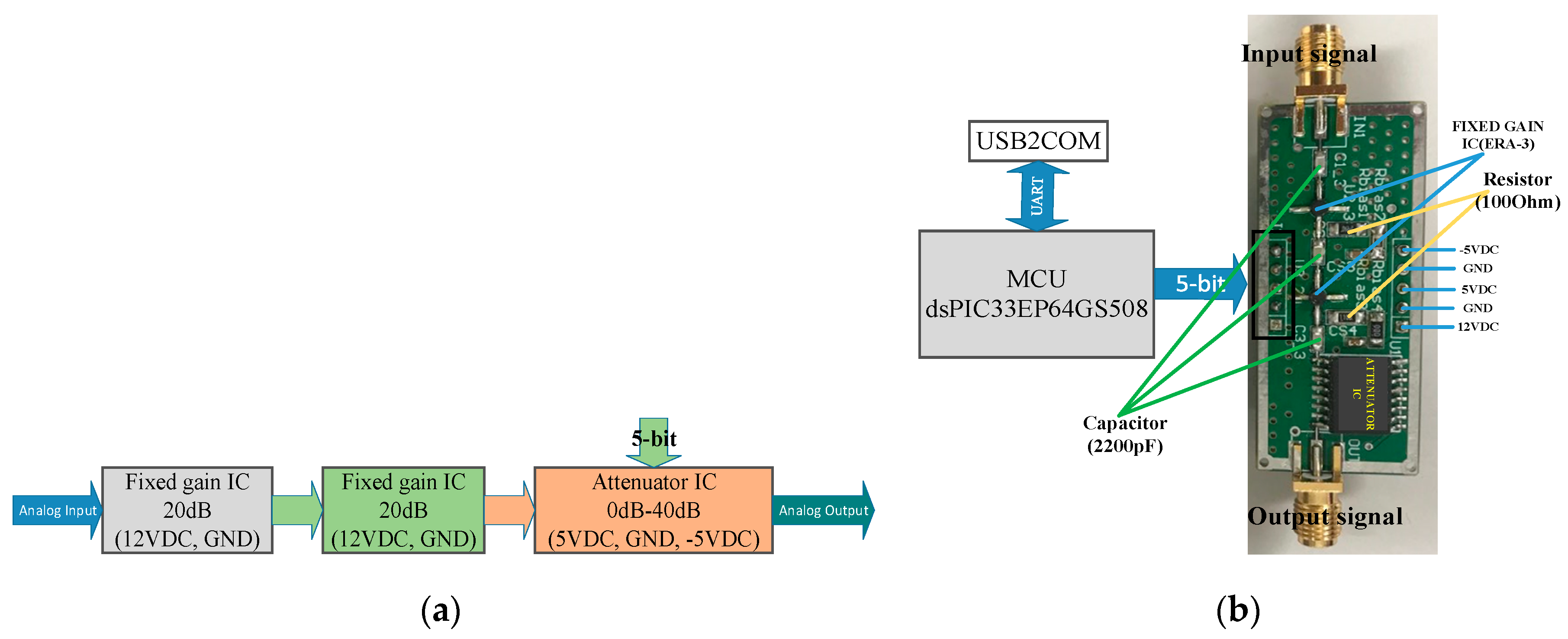
2.5. Solution for Design the Amplifier Module
In this study, we designed a P/R device with four channels that could be operated independently. The signal from these channels was the input signal of the digitizer device used for analysis, so adjusting the amplitude of the signal was important in creating uniformity between channels. The gain amplifier of the channels could be adjusted from 9 dB to 40 dB, which meant we could use many different transducers at the same time.
The echo signal received from the transducer had a relatively small amplitude, so it was necessary to design the amplifier module to amplify the signal before entering it into the analyzer. In
Figure 5, we show the parameters of the components that amplified the amplifier and the hardware after the design was completed [
34].
The gain amplifier was selected from the software. The dsPIC33 chip received the command from the software and then controlled the amplifier module’s gain with a 5-bit resolution.
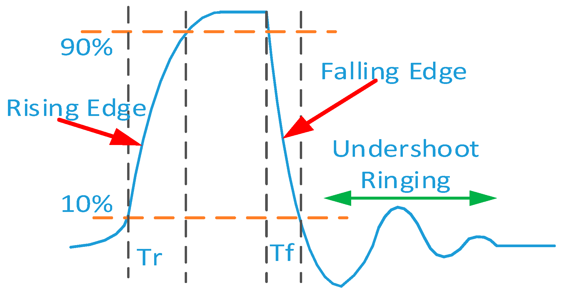
2.6. Unipolar Pulser Generator Analysis
High-voltage unipolar pulses are widely used in ultrasound applications because of their large bandwidth. A unipolar pulse signal is described in
Figure 6. The shape of this pulse is analyzed into 3 parts. The first part consists of logic level 0 (rising edge), the second part is the time when the logic level is highest, and the last part is the overshot of the signal (falling time). For high-frequency transducer stimulation, signals require a small duty to click, thus reducing the rising time and falling time of the signal. In order to reduce these two parts of the signal, the impedance must be matched between the source and the load. At the same time, the signals need to be similar in length.
In this study, we needed to generate a unipolar pulse with a duty of less than 10 ns to trigger the transducer. This unipolar pulse was generated from the FPGA, then entered the input of the STHV800 chip to raise the voltage and trigger the transducer. The rising time and falling time components are described in
Figure 6. To achieve such a signal, we needed to solve four major problems in the PCB design: signal reflection, signal noise, signal crosstalk and signal timing [
28,
35,
36]. To solve these problems, based on the design of the PCB, we needed to ensure the proper values of the following factors: impedance, matching and spacing. The undershoot ringing in particular was solved by selecting damping impedance values suitable for each frequency of the transducer [
37]. Reducing the undershoot ringing was essential for raising the bandwidth of the P/R device.
2.6.1. Impedance Controlled Routing
Stack layer design is one of the most important and effective methods in controlling the impedance of printed circuit lines in a PCB’s design.
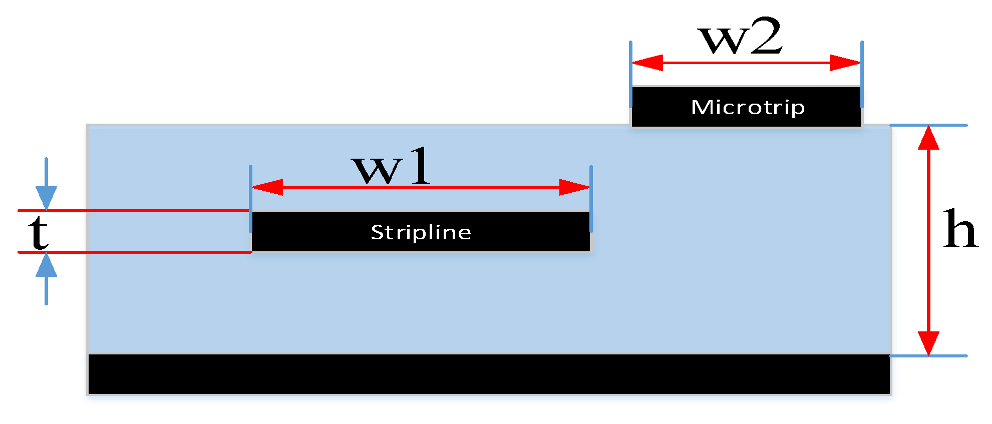
Figure 7 depicts the impedance and propagation delay with two different types of circuit lines, which are narrow microstrips (1 ≤
εr ≤ 15 and 0.1 <
w/
h < 2.0) and narrow striplines (
w/
h < 0.35 and
t/
h < 0.25).
Microstrip layout impedance and propagation delay can be expressed as
Stripline layout impedance and propagation delay ca be expressed as
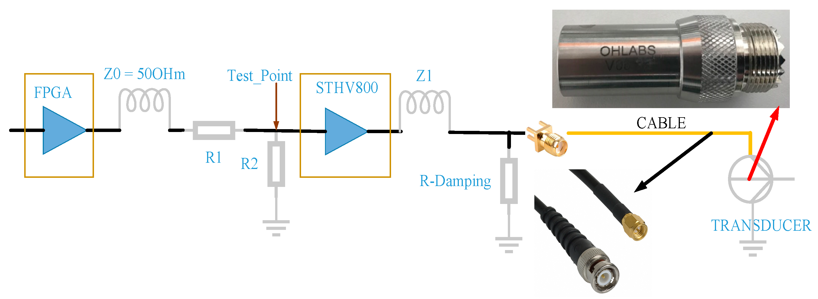
Another method to reduce the reflection of signals on the transmission line uses termination techniques. There are two broad kinds: series termination and parallel termination. Thevenin termination is one of the parallel terminations, shown in
Figure 8. The resistance formula of a Thevenin termination is R1 +
Z0 = R2. Proper termination can reduce overshoots, undershoots and ringing, as well as the amplitude of crosstalk [
38].
To analyze the design, a common rule of thumb is the one-third rise time rule, which states that if the route is more than one third of a rise time long, reflections can occur.
The one-third rise time rule states that the speed at which electrical energy can travel along a route is known as the propagation velocity and can be defined as
where
Vp is the propagation velocity,
C is the speed of light (299.792458 mm/ns) and
εr is the dielectric constant.
Applying the one-third rise time rule, the transmission line effects will begin when
where
LR is the length of a route and
TR is the signal Rise time.
Assume a simple wire require the following calculation:
where
TR is the signal rise time,
TDP is the delay per unit of length,
Lmax is the length of the wire and
delaymax is the wire delay, which is equal to
TDP ∗
Lmax.
The PCB design usually applies two rules to reduce the noise of the circuit board: the 20H rule and the 3W rule. Applying the 20H and 3W rules can reduce the circuit field’s radiation by 70%. The 3W rule represents the approximate 70% flux boundary at logic currents [
39]. In this design, to reduce the impact of crosstalk noise on the pulse signals from the FPGA with the STHV800, we applied the 3W rule.
Table 2 describes the signal connection between the XC6XLX9 and the STHV800.
2.6.2. Power Integrity Design
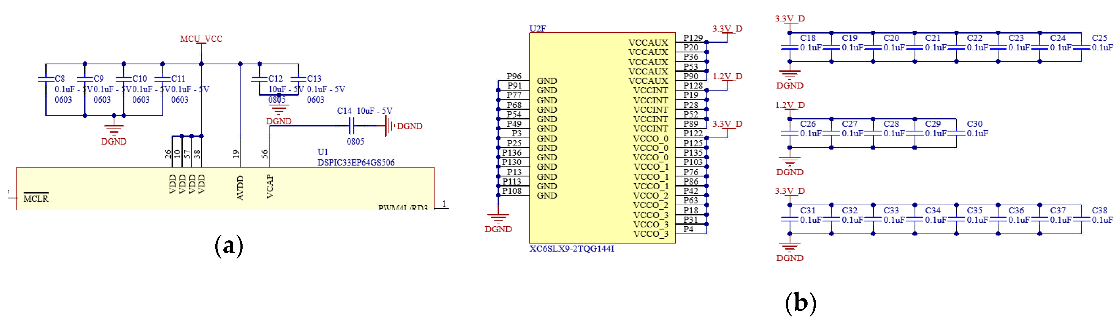
Using the signal integrity (SI) analysis method resulted in signal lines on the PCB to ensure signal integrity. However, energy integrity was a major issue that needed to be considered, especially for high-speed PCB types. Power integrity (PI) analysis indicated that interference from the power supplies greatly influenced signals in the high-speed systems. The noise voltage caused by the transient current made the supplying power continuous and even affected the normal work of the high-speed system. At present, PI issues have two solutions: optimizing the layer stack structure of the PCB and placing decoupling capacitors on the PCB.
In addition, we applied proper bypass capacitors and separation techniques to improve the overall power supply SI. A series of capacitors should be used to eliminate the effects of source voltage interference with the two main chips (FPGA and dsPIC33EP64GS508) in this design. Small decoupling capacitors with low current inductances could provide fast current to high-frequency converters. The average bypass capacitor could filter out noise, preventing them from entering the IC. Bulk capacitors continued to provide current after the high-frequency capacitors exhausted their energy storage. The application of these capacitors to the design is described in
Figure 9.
A good layer stack structure may be the best solution for most SI and electromagnetic compatibility (EMC) issues. Ground planes are an effective EMC shield, good image planes can be good return paths, and small loop areas reduce electromagnetic interference radiation. The closer the power plane is to the ground plane, the bigger the capacitance, and the lower the impedance, the better the reduction of switching noises.
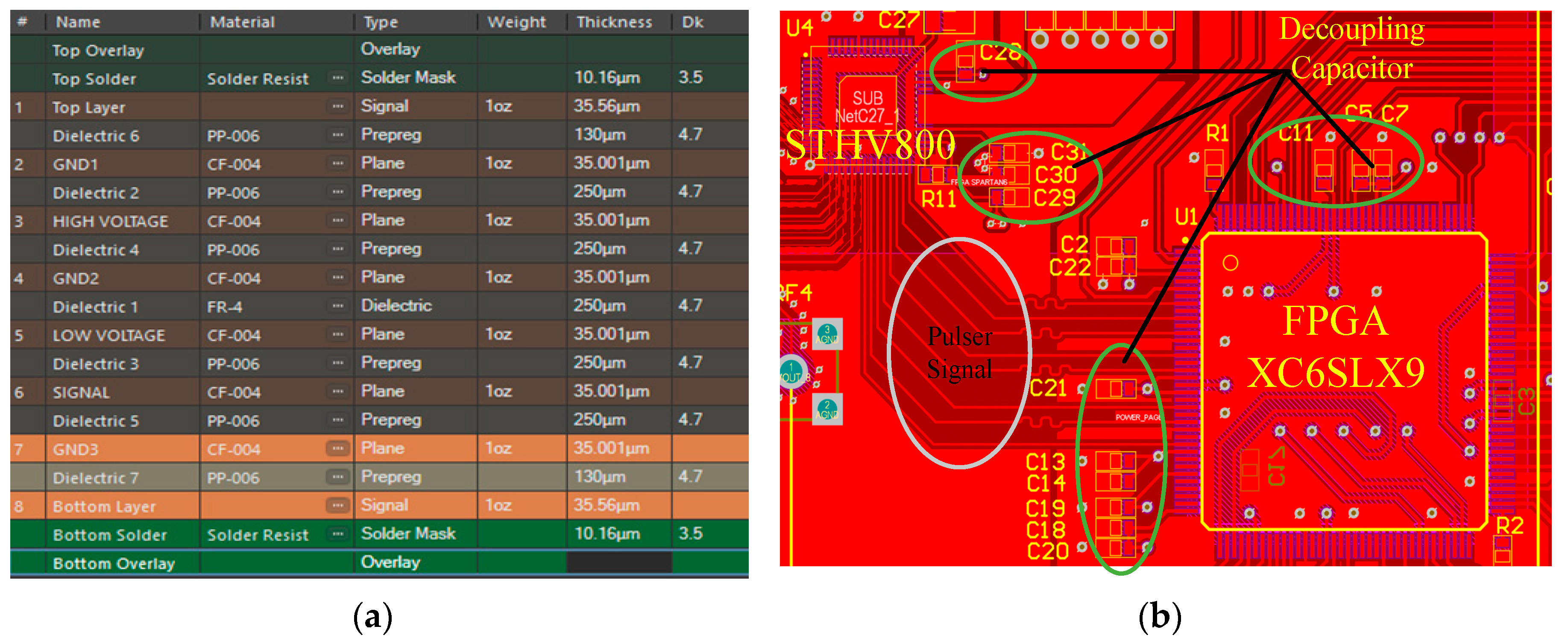
In this design, we used the eight-layer PCB with the stackup, as described in
Figure 10. With this stackup, the impedance of the signal classes was calculated and matched with an impedance of 50 Ω. In this stackup, the third layer (high voltage) and the fifth layer (low voltage) separated. The layout of the source for the STHV800 chip had been optimized by us. The second layer (GND1, mainly ground for the dsPIC33EP64GS508, FPGA, …), fourth layer (GND2, mainly ground for the low voltage of the STHV800) and seventh layer (GND3, mainly ground for the high voltage of the STHV) were the plane layers. We separated these layers to limit interference from the source.
The layout design of the decoupling capacitors for the two main chips (FPGA and STHV800) are presented in
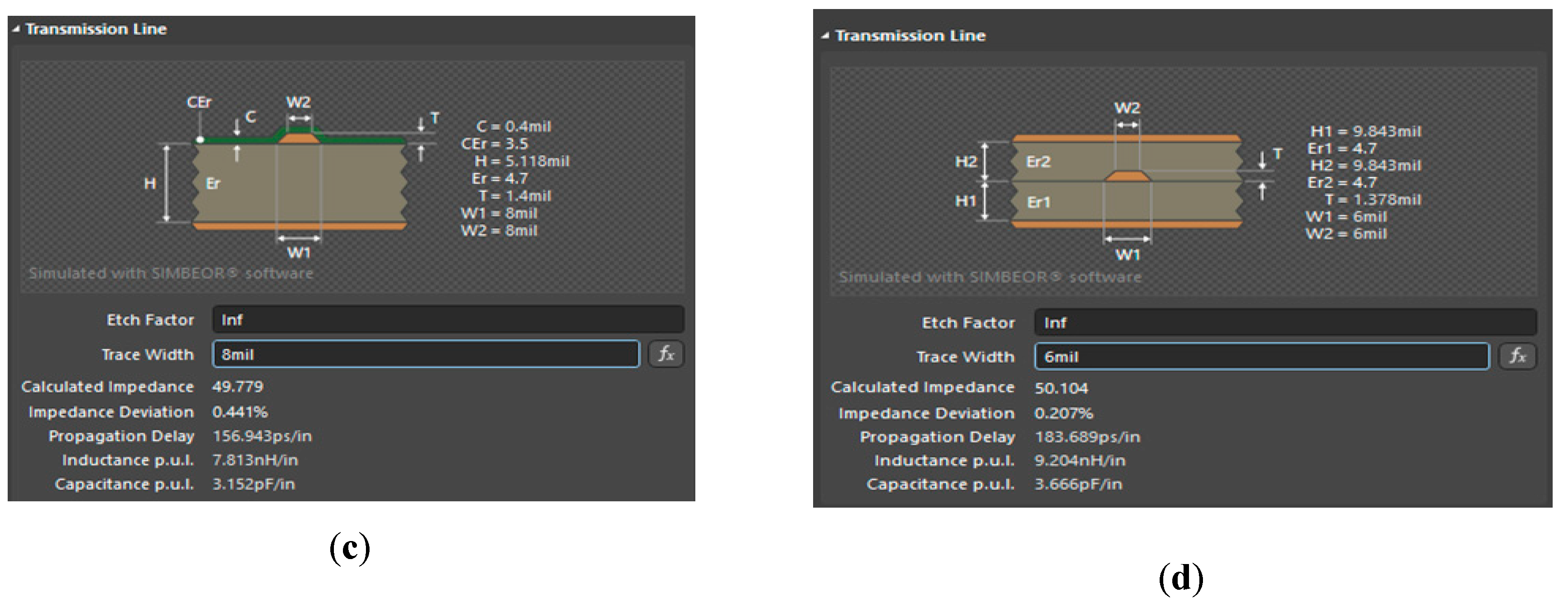
Figure 10b, and the impedance of the microstrips and striplines are shown in
Figure 10c,d.
2.6.3. Optimized Damping Resistor for High-Frequency Transducer
The techniques of matching impedance and PI are very effective with the onboard signals that help reduce overshoot and undershoot and optimize transmission power. The length of the cable between the transducer and the P/R device has not been determined (regarding the length of the cable and the impedance and frequency of transducer operation). As such, in this section, the damping resistance values need to be optimized for a different transducer type.
Figure 8 shows the position of the damping resistor in the P/R device. However, the transducers do not match the impedance, so the use of damping resistors is important in improving the transducer’s vertical resolution.
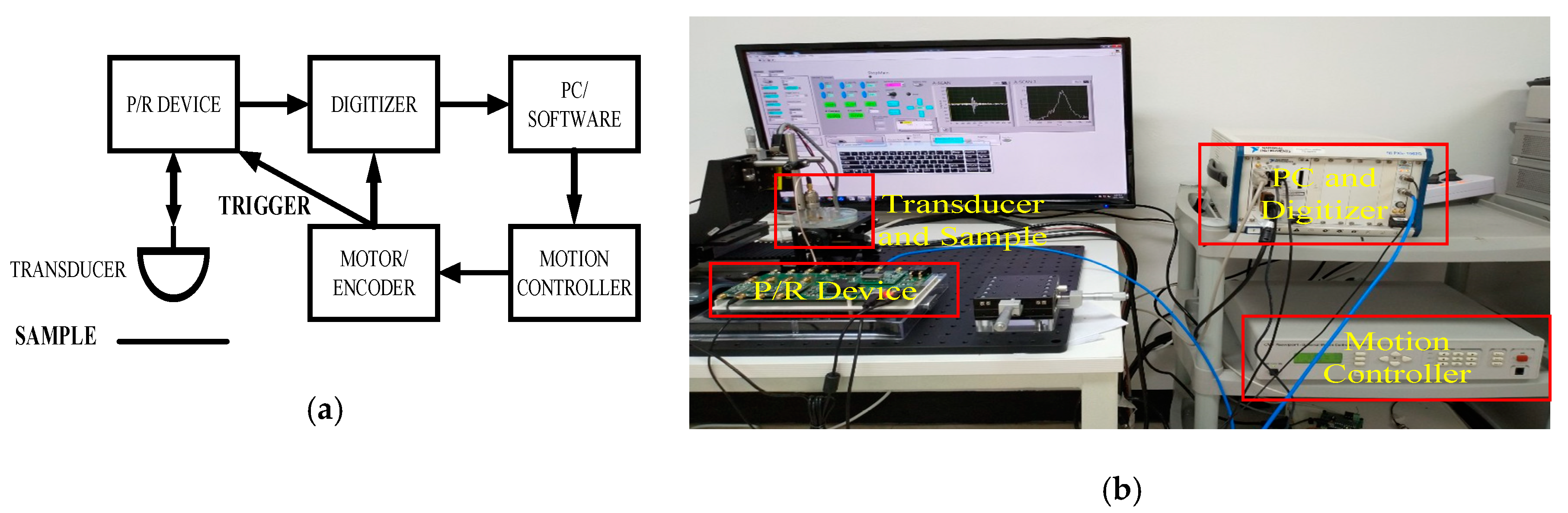
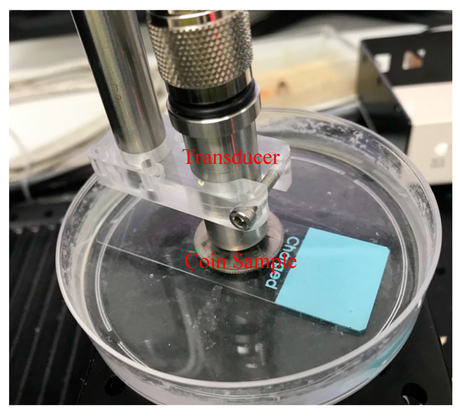
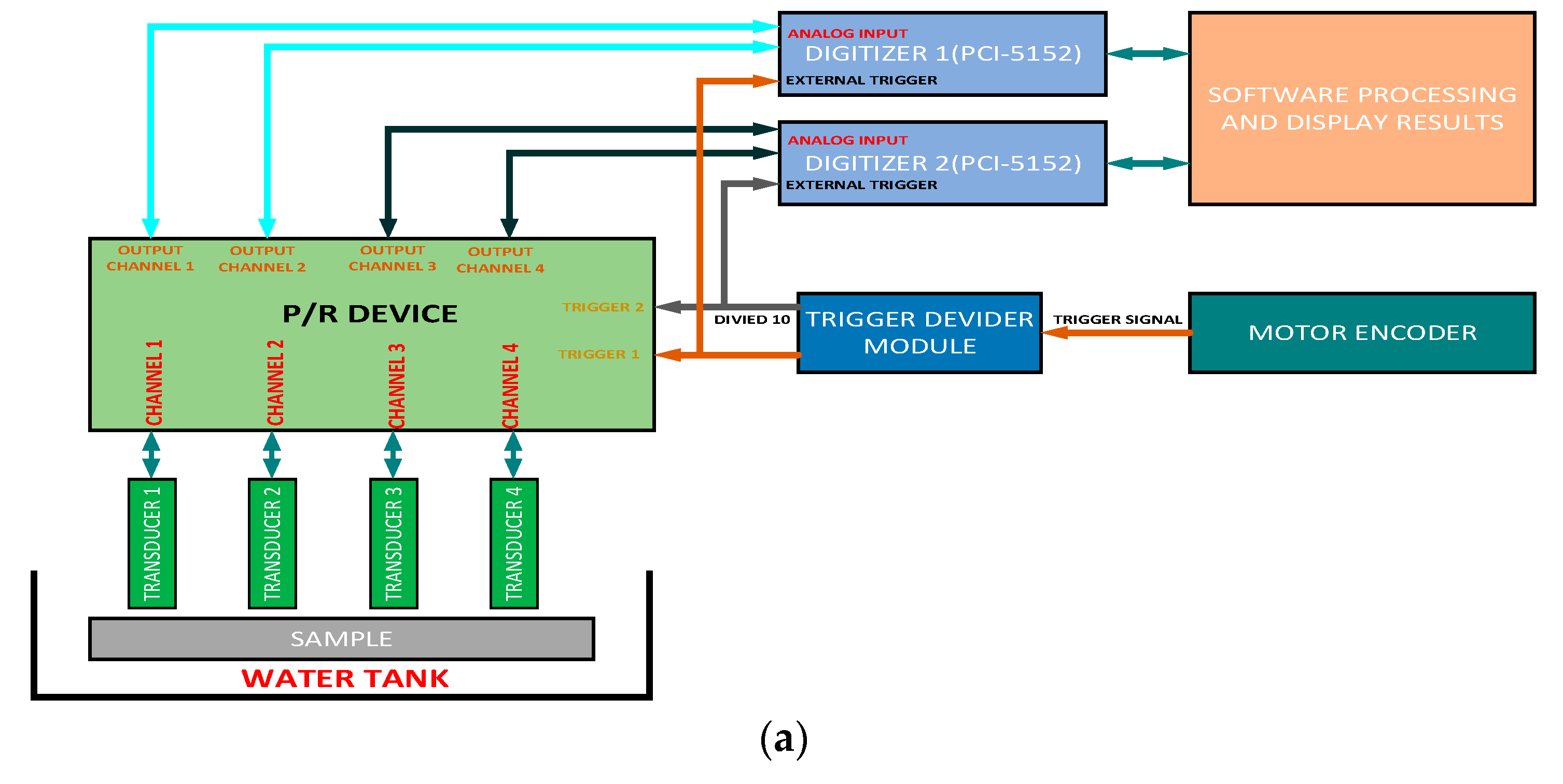
4. Implementation System and Results
After completing the hardware design, as well as acquiring the firmware and software needed for our system, we set up the SAM system to test the P/R device. The system model is described in
Figure 14a, and the real model of the system is described in
Figure 14b. The system test with the P/R equipment was divided into two parts. The first part was setting up and checking the signals that were designed and programmed with the transducer and the class sample. The second part tested the SAM system when scanning samples with the techniques applied above.
4.1. Unipolar Pulser Generator
As we mentioned above, the pulse optimization for the probe was done in two parts. The first part, performed on the included PCB design, ensured the integrity of the trigger signals from the FPGA to the STHV800. Since the transducer impulse had a duty of only a few nanoseconds, the rising time portion was also a value of a few nanoseconds. We applied techniques such as calculating the characteristic impedance of the circuit, as in Equations (1) and (3), and calculating the length of the printed circuit and used thenvenin resistors to reduce the reflection of the signal. (Altinum Designer software also provide the signal integrity simulation feature to shorten the time and improve the efficiency of the design). Besides that, we placed decoupling capacitors near the FPGA and the STHV800 to reduce the noise interference when they were working. For the second part, we used a damping resistor for the signal from the STHV800 to the transducer. The value of the damping resistor had been determined by tests because the impedance of the transducers may have differed.
The trace width and resistor values used in the design are described in
Table 3.
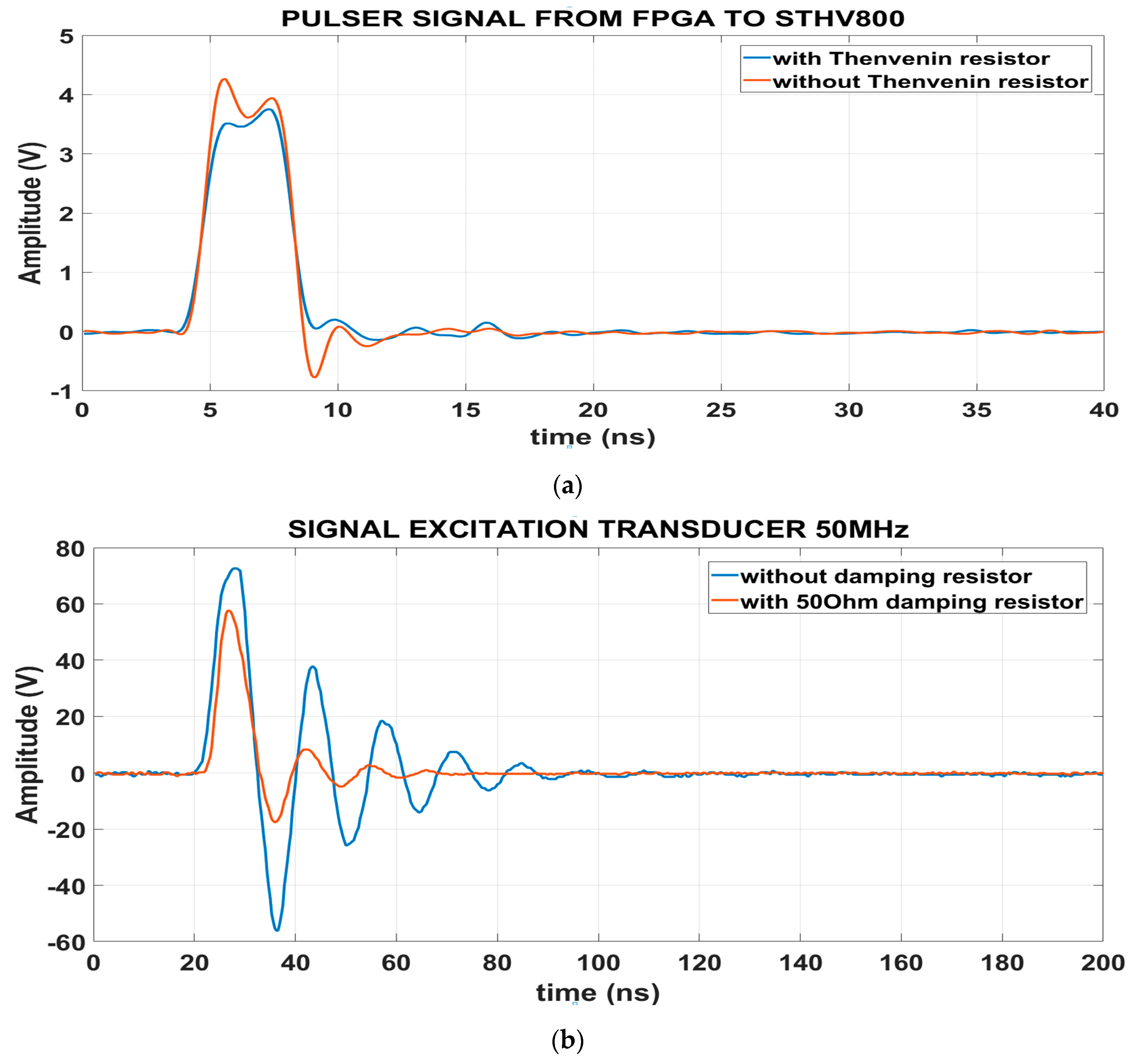
In this test, we measured the unipolar pulse signal generated from the FPGA chip to excite the STHV800 chip and evaluated the effectiveness of the techniques used in the PCB design with this signal. As mentioned above, we used the schematic described in
Figure 8 to design the signal from the FPGA to the STHV800 and set the signal of the excitation transducer 50 MHz. The measurement point is denoted as Test_Point. We used a KEYSIGHT oscilloscope, model MSO-X2024A, to monitor the signal.
After a thorough analysis and comparison of the unipolar pulse signals in
Figure 15, we can see that this signal improved. The undershoot part of this signal had been reduced significantly, which was essential in increasing the transducer signal’s bandwidth. In
Figure 15b, we see clearly that the damping resistor effect reduced the signal amplitude, but at the same time, the ringing part of the signal was also clearly reduced. This had important implications for detecting different layers of the object to be scanned because for many samples with many layers, there are often many echo signals received, and creating the vertical resolution of the sample depends on these echo signals. In
Figure 15a, we compare the signal before and after adding damping resistors, the signal from the FPGA to the STHV800 had reduced overshoot and ringing with damping resistor. We could easily change the pulse width by changing the variables in the FPGA with the software to make a signal suitable for different transducers.
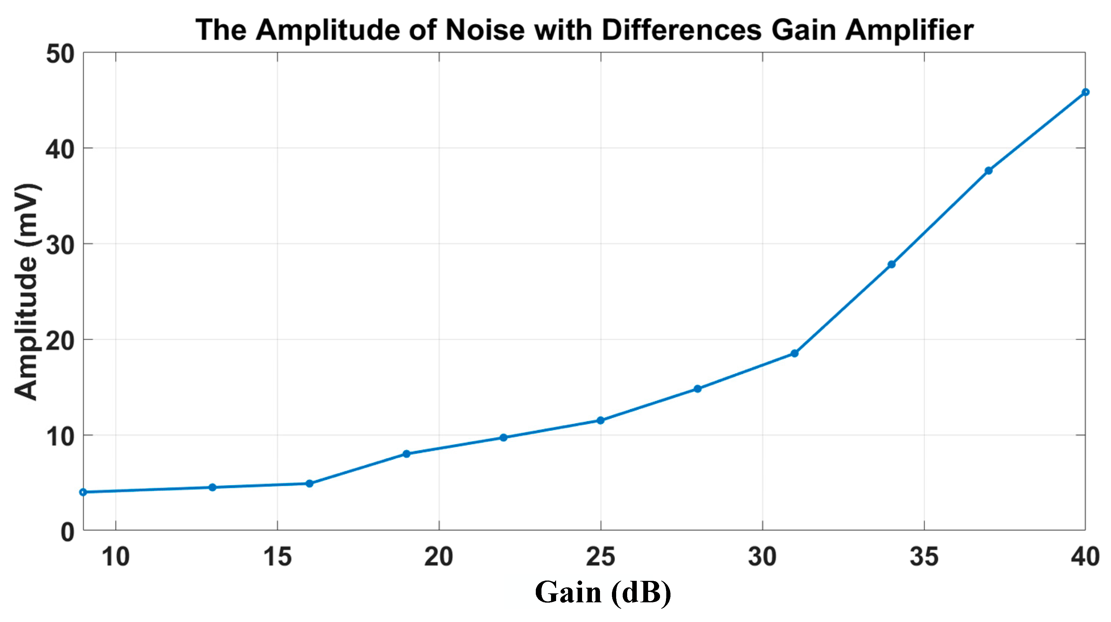
4.2. Tested Background Noise of the P/R Device
In this test step, we measured the background noise amplitude of the P/R device with different gains from the amplifier module. The goal of this test was to check the P/R device’s interference amplitude under normal operating conditions. These results also evaluated the effect of environmental interference on the device when combined with other components of the SAM system. The results are depicted in
Figure 16. As the gain increased, the noise amplitude increased, but the maximum amplitude of the noise was 45 mV. Usually, these values are quite small relative to the amplitude of the echo signal. This result was important for identifying and eliminating interference from other devices that could affect the echo signal.
We ran tests with different echo signals. The maximum amplitude of the echo signal was about 3.5 V. The echo signals, after going through the amplifier module, had amplitudes higher than 3.5 V, but then the output signals were distorted.
4.3. Optimized Value of the Damping Resistor
As mentioned above, in this section, we will determine the damping resistor values best suited to the transducers of predetermined frequencies. We used the same experimental model as in
Figure 15b. We replaced the PC and digitizer with an oscilloscope (MSO-X2024A) to observe the transducer’s echo signal. This test result is presented in
Table 4.
For the sample thickness, applications used ultrasound signals. The damping resistor was used to reduce the ringing portion of the first echo signal so that it was easy to detect the second echo signal. We chose for the gain of the amplifier module on the P/R device to be 40 dB and the excitation voltage to be 90 V.
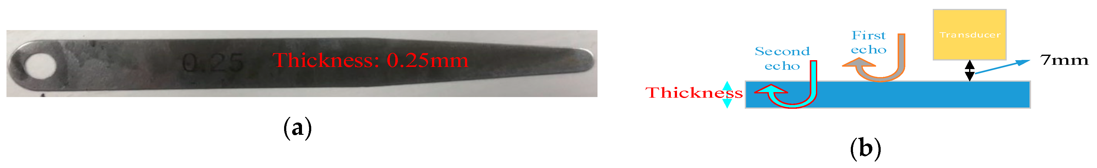
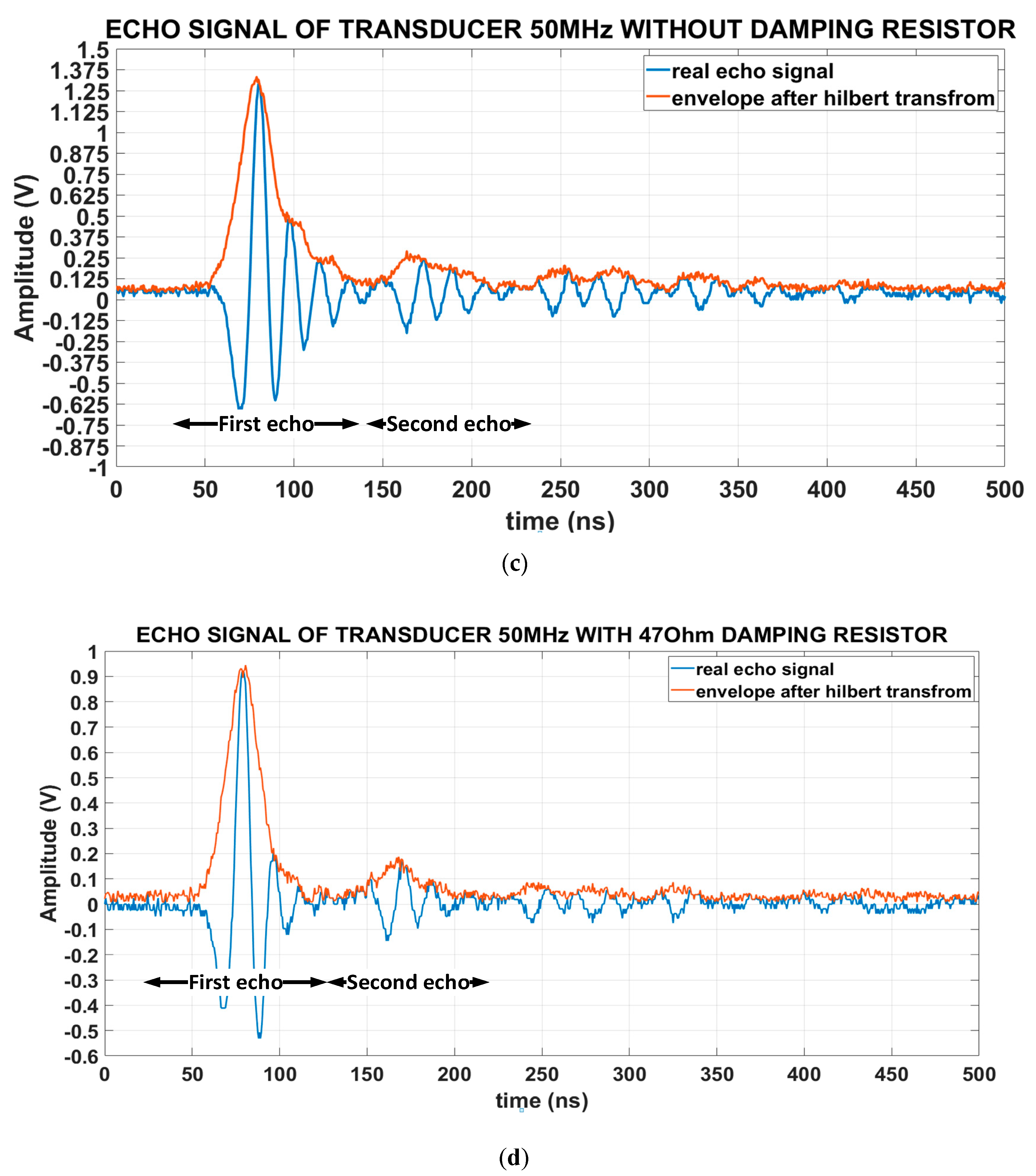
As shown in
Figure 17a, we describe a sample of steel which had a uniform thickness of 0.25 mm. In
Figure 17b, we describe two echo feedback signals from the upper and lower sides of the sample to the transducer. In
Figure 17c,d, we describe the echo signal measured on the oscilloscope of the 50 MHz transducer with and without a 47 Ω damping resistor.
Based on the echo signal described in
Figure 17c,d we can see the function of the damping resistor when detecting echo signals close to each other. In
Figure 17c, the transducer without an additional damping resistor made it difficult to identify the second echo signal because the ringing part of the first echo signal was too long. In
Figure 17d, the transducer had a 47 Ω damping resistor added on the ringing part of the suppressed first echo signal, and it was easy to identify the second echo signal. This was because it depended on the characteristics of the transducer used in the experiment.
On the other hand, we computed the signal-to-noise ratio (SNR) of the signal depicted in
Figure 17c,d. The results are shown in
Table 5.
The results in
Figure 17c,d and
Table 5 show that the amplitude of the echo signal was reduced after applying the damping resistor. However, the damping resistor also suppressed a number of other reflected signals. Thus, this increased the SNR ratio of the echo signal. This also increased the quality of the B-mode images.
4.4. Testing with the SAM System
As described in
Figure 15, the SAM system transmits and receives signals based on the signal from the motor encoder (this is also the trigger signal for the P/R and the digitizer). The SAM system consisted of three main devices: a PC and digitizer (NI PXIe-1062Q and NI PXI-5152 8-bit, 2 GS/s digitizer, National Instruments Corporation. Austin, TX, USA), a Newport Driver (Model ESP300, Newport Corporation. Irvine, CA, USA), and our P/R device. Therefore, the higher the pulse frequency from the encoder, the faster the sample scan time. In our design, the trigger module of a P/R device could receive pulses of up to 100 kHz.
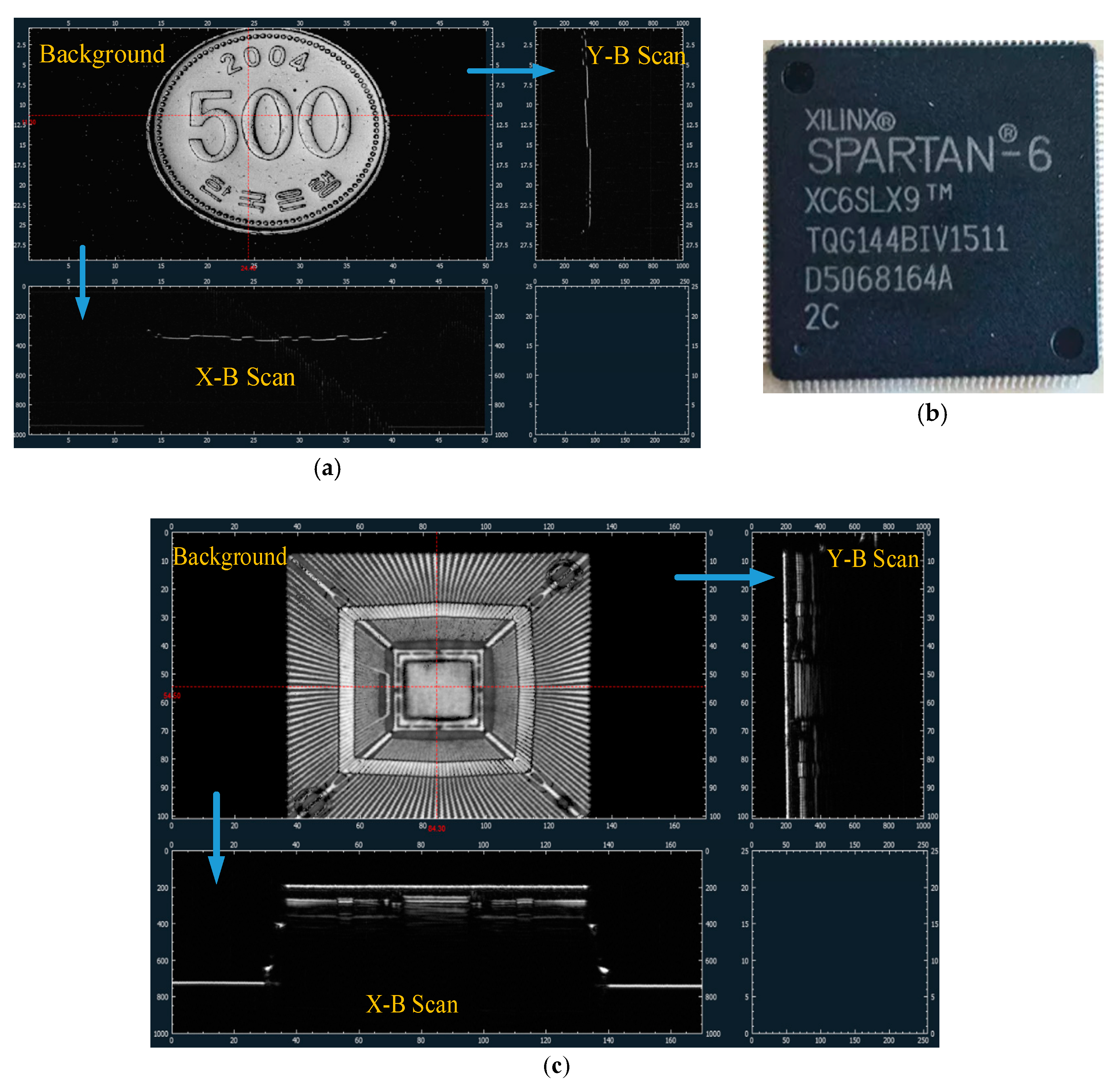
In this test, we used an image acquisition system to test the signal with a sample of one coin. The parameters for setting up the scanning system are described in
Figure 18 and
Table 6.
On the other hand, we conducted experiments to determine the SNR ratios of two different transducers. This test was done before the system’s scan of the coin. The results are described in
Table 7.
In
Figure 19, we described the system’s final image with the use of damping resistors. The images obtained for systems using suitable damping resistors were of a high definition due to the improved SNR of the echo signal.
In
Figure 19a, we scanned the surface of the coin and used a high-frequency transducer (85 MHz). High-frequency transducers with poor sample penetration are suitable for surface scanning applications. In
Figure 19c, the inner layer of the Spartan-6 chip is described. We used a 25 MHz transducer to do this experiment. The ultrasonic waves generated by the 25 MHz transducer penetrate the object better than the 85 MHz transducer. Hence, the SAM system using the 25 MHz transducer obtained a better image than the SAM system with 85 MHz transducer.
After performing the coin scan, we calculated the contrast-to-noise ratio (CNR) of the obtained image. The results are described
Table 8.
Based on the results in
Table 7 and
Table 8, we can see that the damping resistor increased the SNR of the echo signal from the transducer. The CNR of the image was also improved after using damping resistors.
4.5. Scanning Sample with Four Transducers at the Same Time
One of the highlights of our design is its ability to operate with four transducers simultaneously. With this capability, the SAM system reduces the uptime by only a quarter compared with that of using the UT320 equipment. Moreover, the maximum trigger frequency of the UT320 was 20 KHz, compared with our P/R device’s 50 KHz. That means the SAM system that worked with our equipment had the highest possible speed, which was 10 times faster than the SAM system using the UT320. Moreover, the highest amplitude of the echo signal from our P/R is 3.5 V, and the UT320 is 1 V. The echo signal with high amplitude create high resolution for B-Mode images. Below is
Table 9, comparing the main parameters.
In this test, we used another SAM system. The new system could work with four transducers simultaneously and used two digitizers, which had two analog channels (PCI-5152, National Instruments Corporation. Austin, TX, USA). The motor control modules were similar to the old system. The new system model is described in
Figure 20.
As is shown in the model of the system in
Figure 20a, the sample was divided into four regions with similar areas. We performed experiments many times with different transducers, and the results are described in
Figure 20c.
In the test, the trigger signals for the P/R and Digitizers 1 and 2 were completely the same. Besides that, we also used four completely identical transducers. The gain of four amplifier modules on the P/R device was adjusted differently. The trigger signals entering channels 1 and 2 of the P/R device and the digitizers were similar. This sample scan result is described in
Figure 20c.
Based on the resulting image in
Figure 20c, we can see the signal uniformity of four different regions of this sample. Each transducer scanned a region, so the time to scan this sample was also four times faster than using a transducer.
5. Conclusions
We proposed a multifunctional pulse generator for SAM systems with a reconfigurable and compact design. The unipolar pulse scheme could achieve a high peak amplitude, on top of the relatively high bandwidth of the device. The system implementation in a PCB scheme allows for a cost-effective and compact design. The reconfigurable structure is versatile for various applications and allows incorporation into open platforms for future research and development.
This article also presented a detailed and complete model of a P/R device used in SAM systems. The important modules required from high technology are clearly stated in the design. The P/R device is designed with four channels, which means that the speed of image scans in a SAM system can be increased four times, compared with that of a single-channel system. Independent gain adjustment channels also create a different resolution in each region. A high resolution is also important when one crucial area needs to be carefully monitored.
The techniques in PCB design with high-frequency signals are applied effectively in this design to help improve the signal and increase the bandwidth of the signal. Besides that, this paper also makes major contributions to systematizing each of the essentials in the design of P/R equipment for SAM scanning.
One of the other outstanding contributions is a summary of the tested and statistical damping resistor values for different transducers. These have significant implications for users operating systems that use this type of equipment. Saving setup time and adjusting parameters, as well as optimizing the achieved results, help produce brighter and sharper images. Tests have shown the apparent impact of these damping resistors in enhancing the SNR of the signal echo. The echo signals from layers of the sample are also distinguished more clearly, thereby improving the resolution between layers while the system scans samples with multiple layers. The image results have increased CNRs, which increase image quality.
The design can expand to have eight channels active at the same time. This means that the SAM system will reduce the scan time of a sample by many times, compared with systems that only operate with one or two channels. This has important implications for production carried out on production lines.

 ,
, 


