Power Line Interference Reduction Technique with a Current-Reused Current-Feedback Instrumentation Amplifier for ECG Recording


Abstract
:Featured Application
Abstract
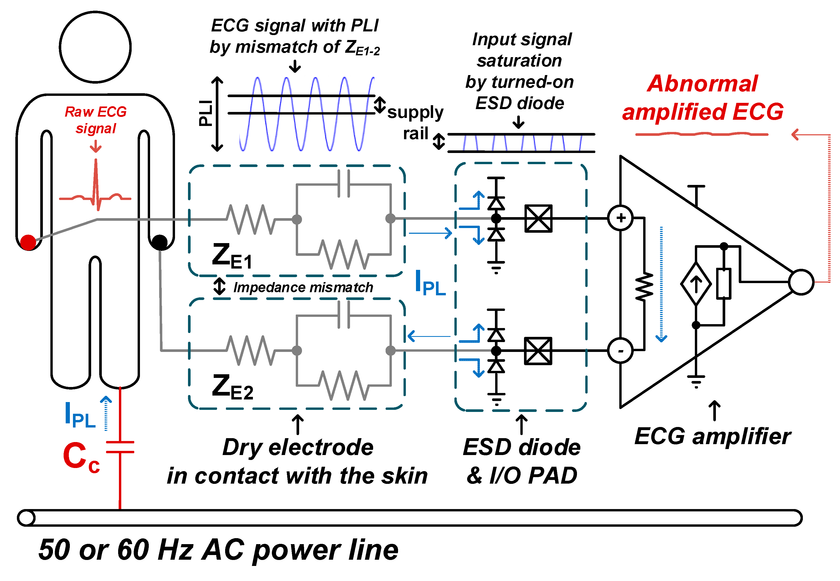
1. Introduction
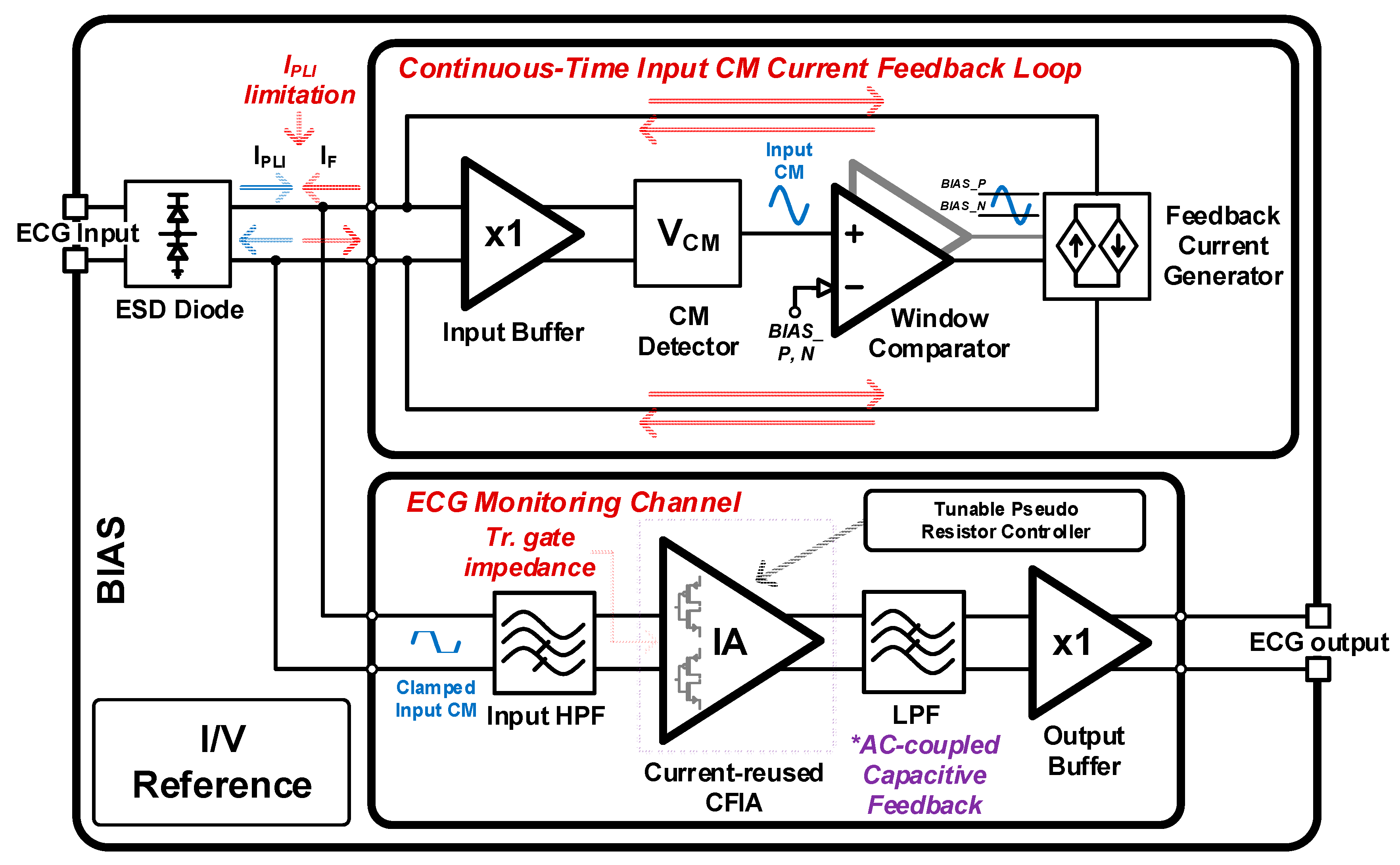
2. Circuit Implementation
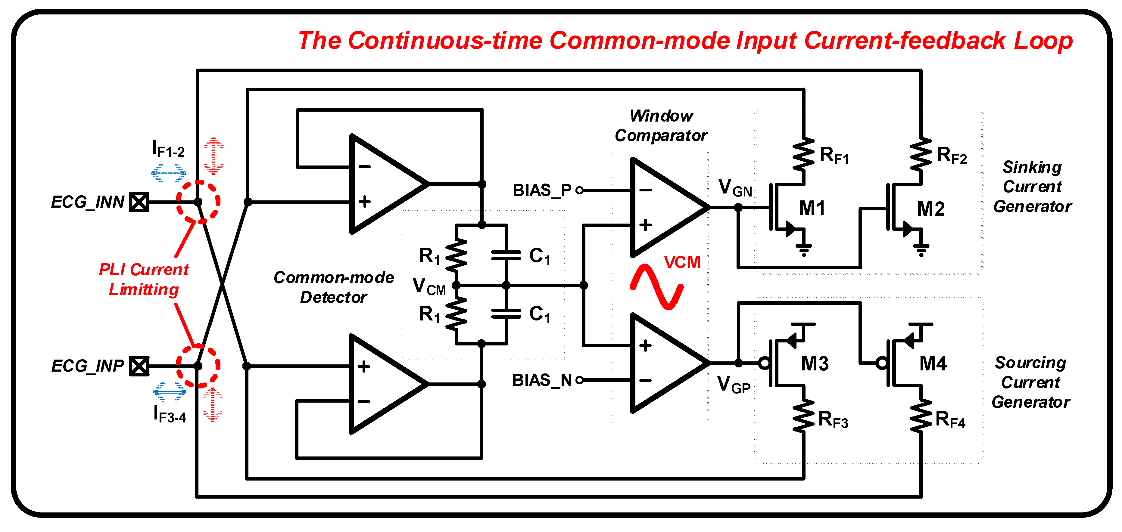
2.1. The Continuous-Time Input Common-Mode Current-Feedback Loop
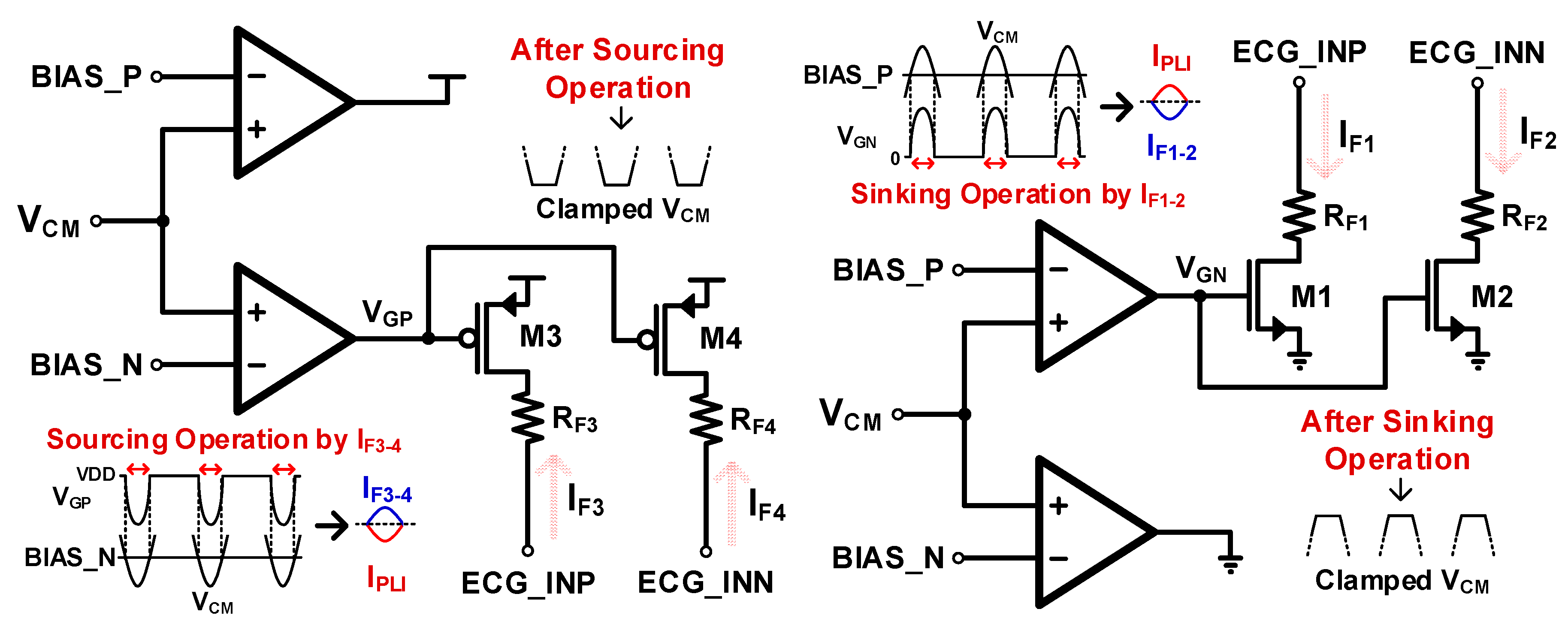
2.1.1. Detailed Description and Operating Principle
2.1.2. Buffer and Window Comparator
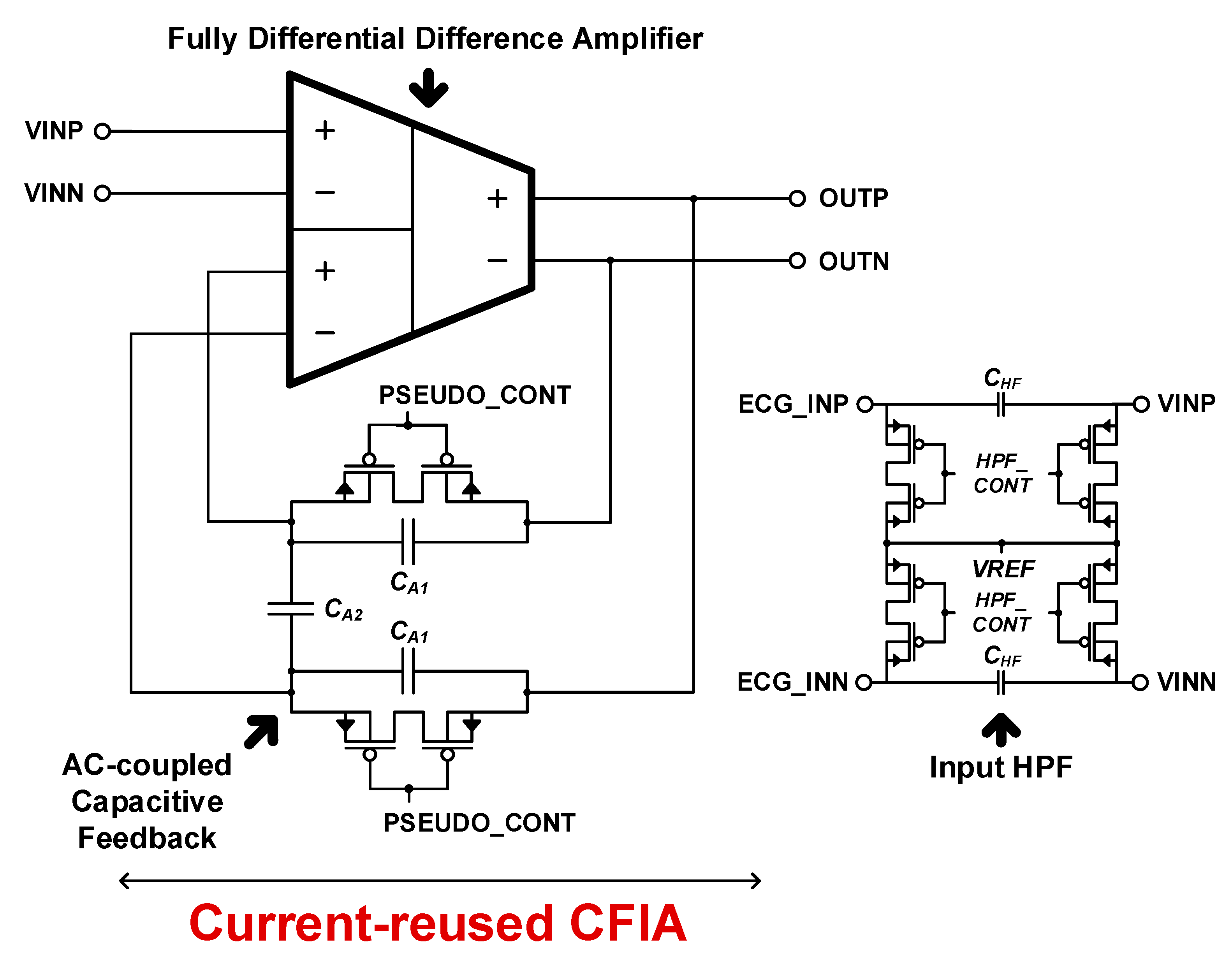
2.2. ECG Monitoring Channel
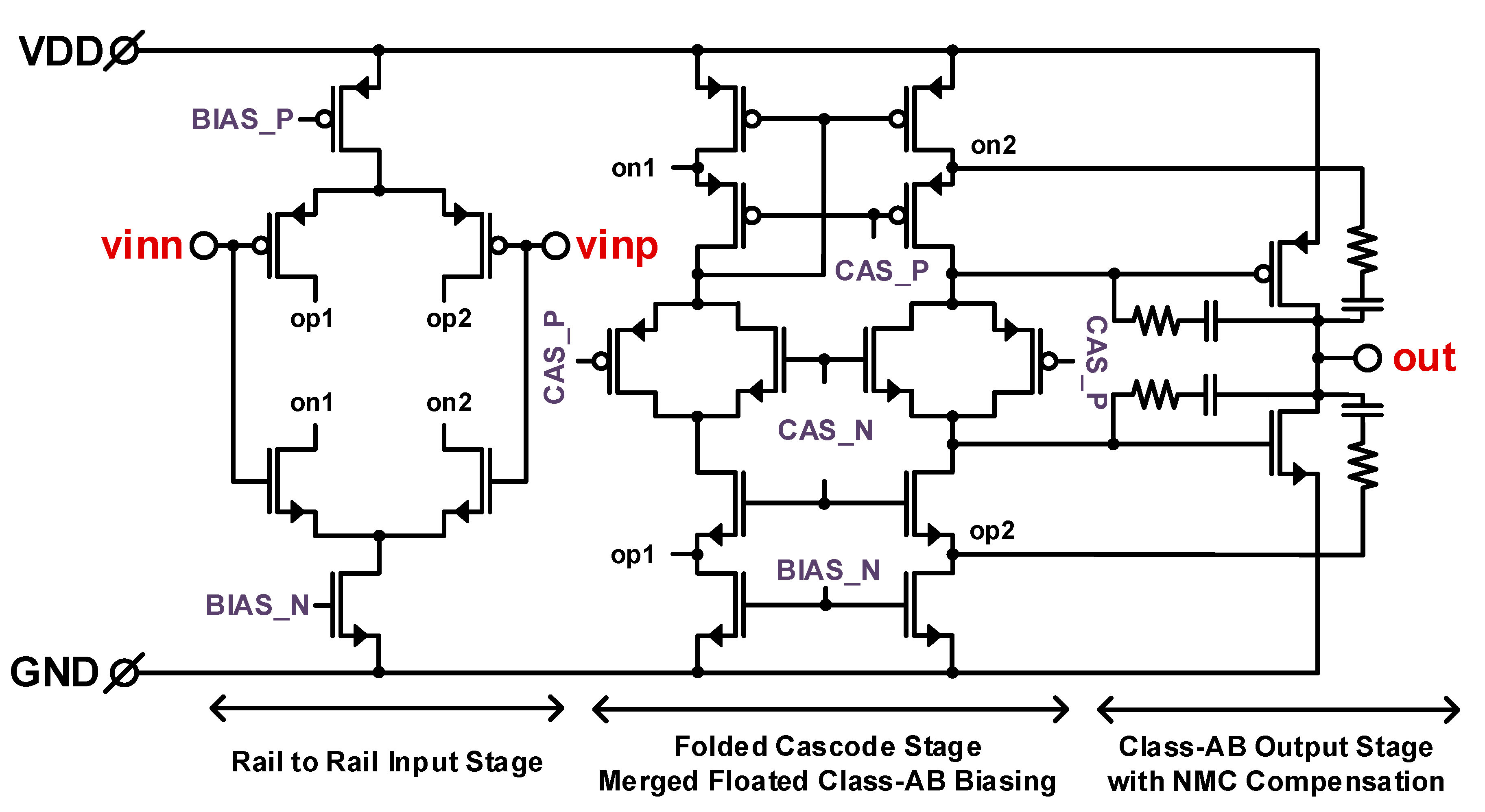
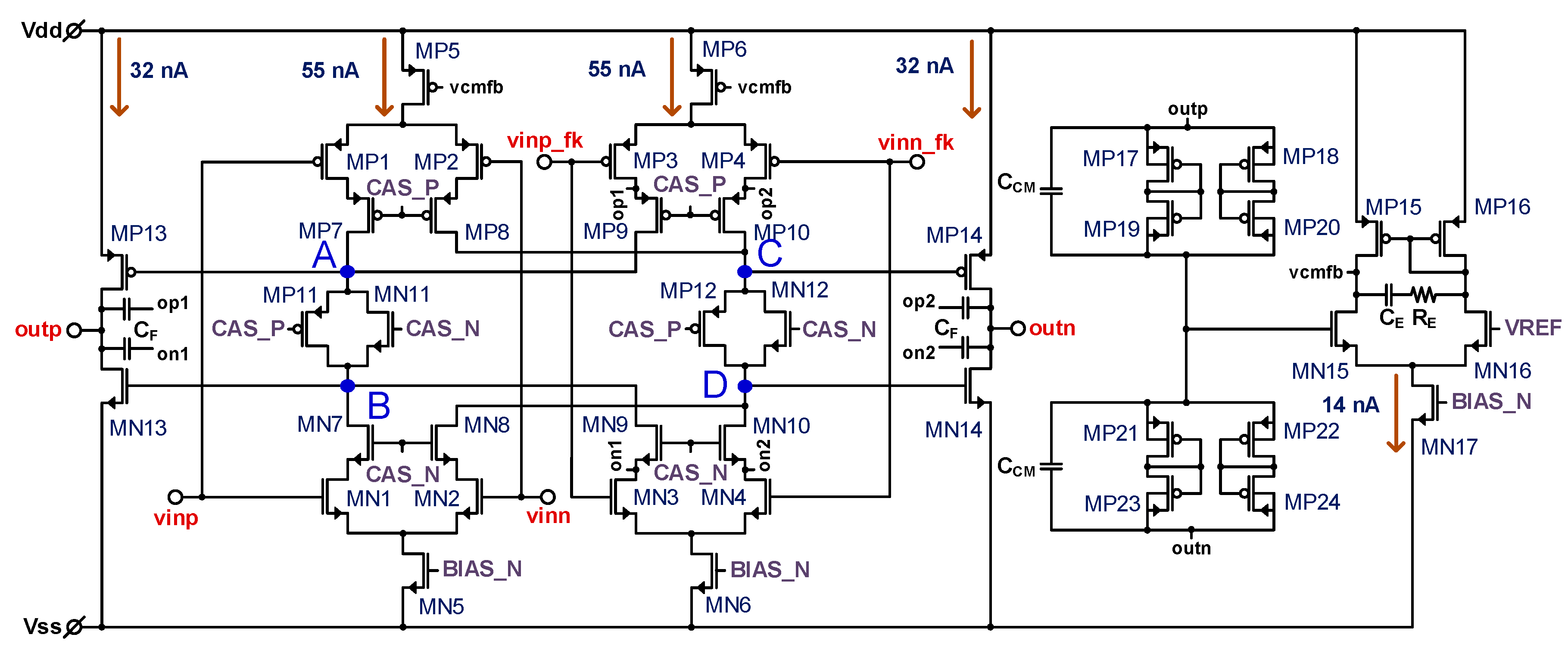
The FDDA in the Current-Reused CFIA
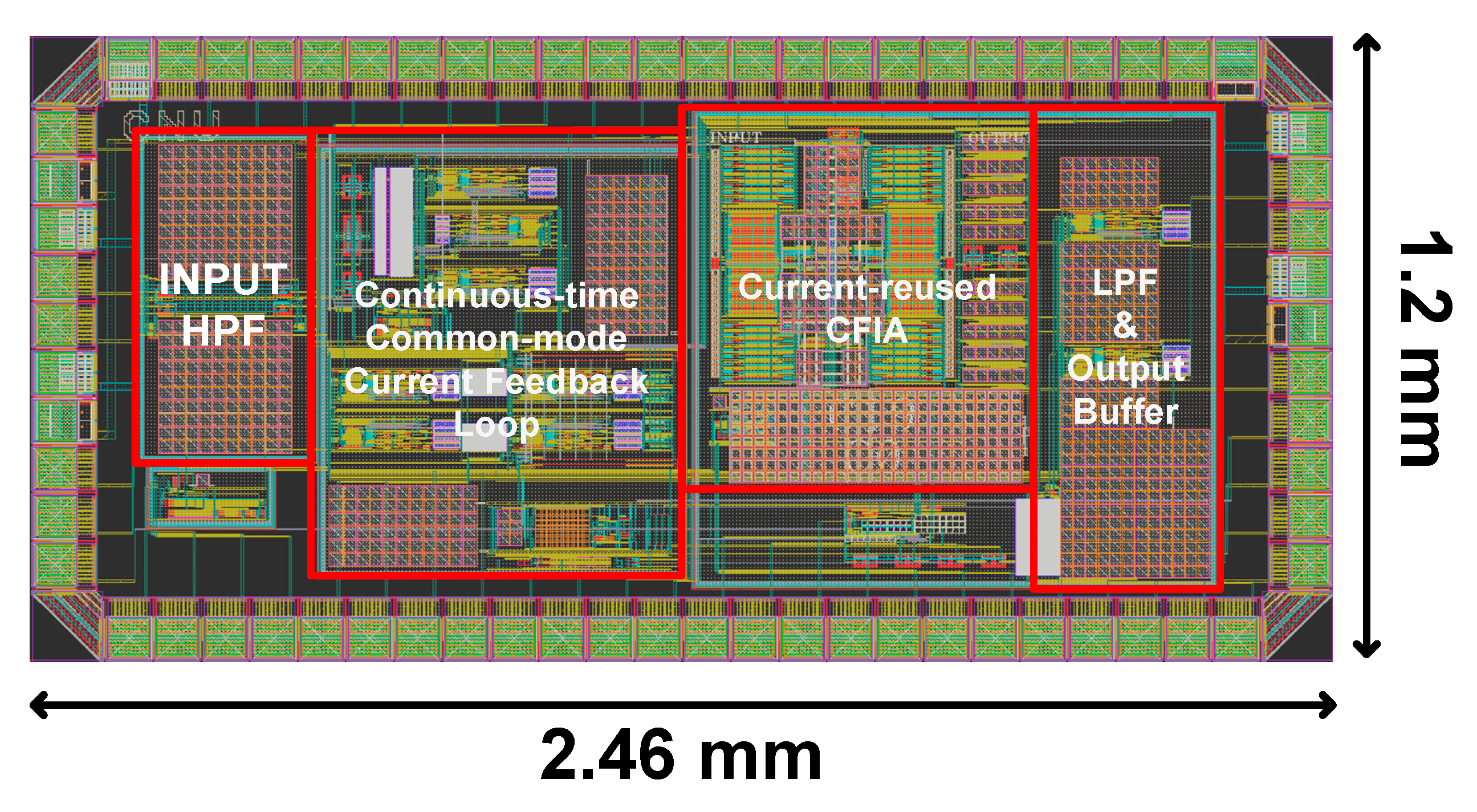
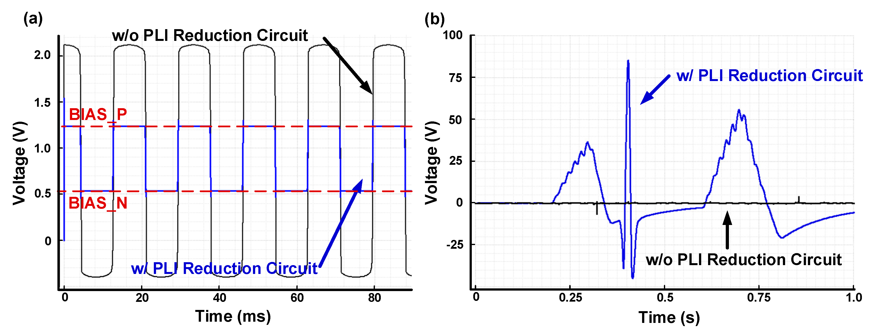
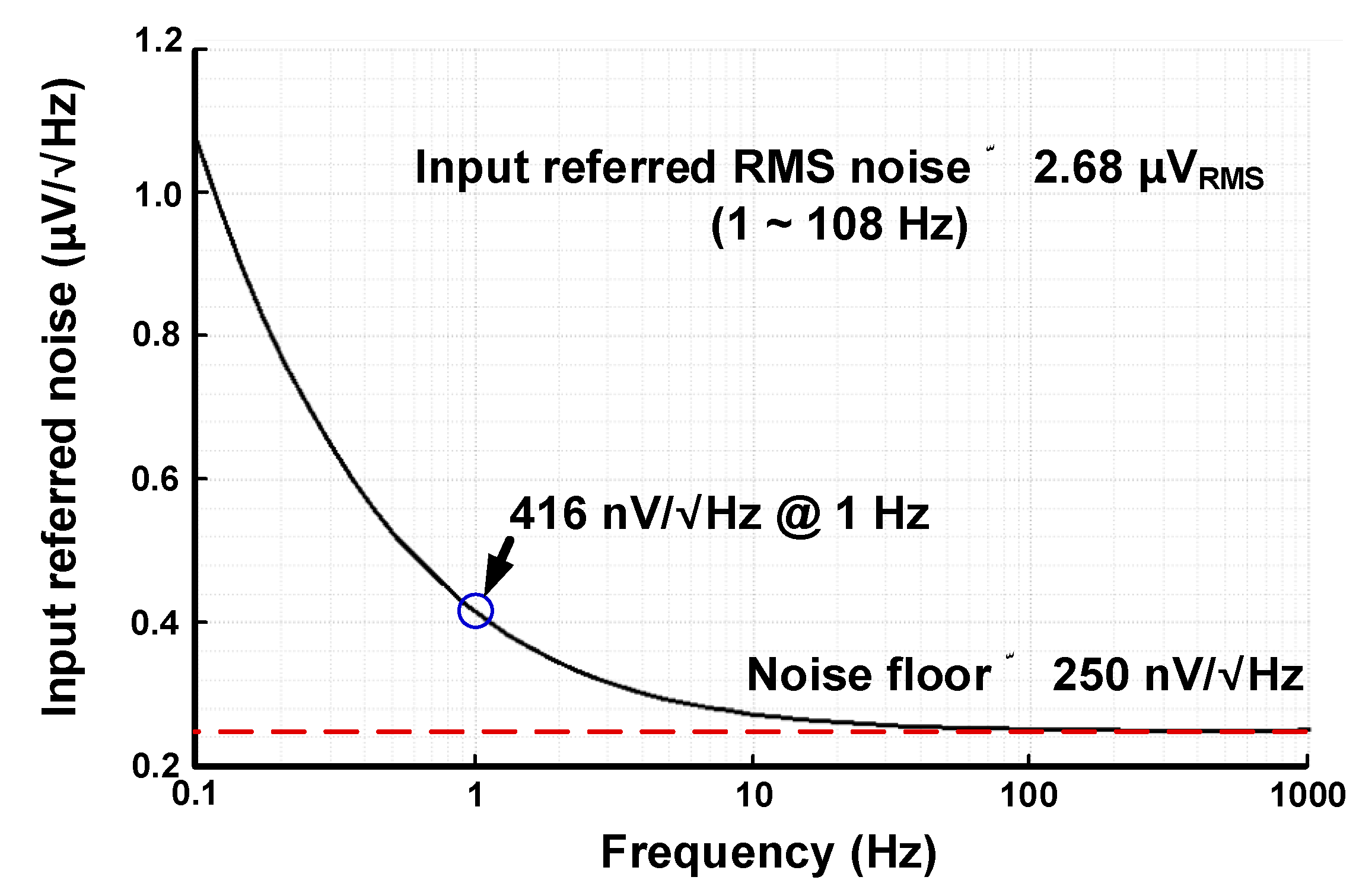
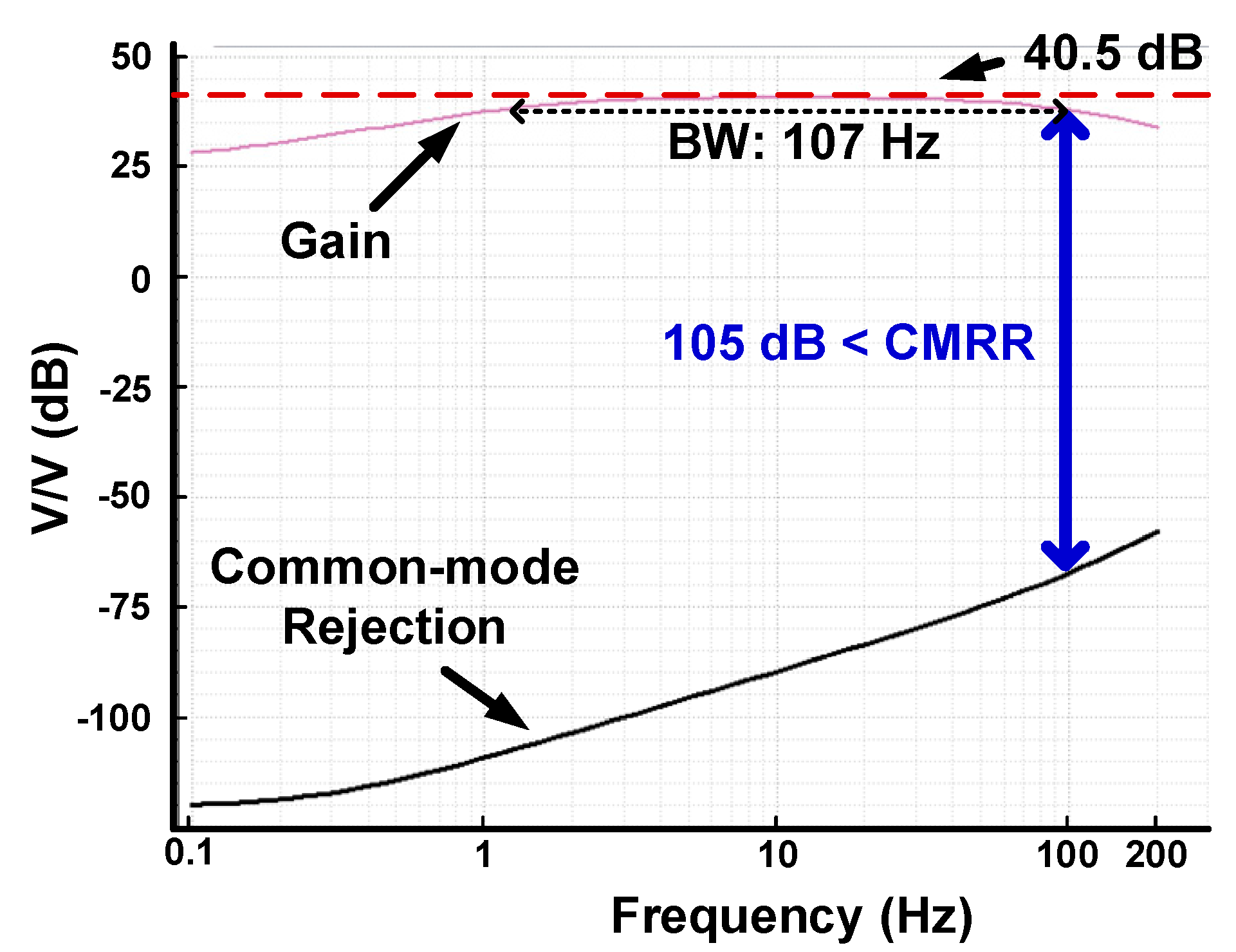
3. Simulation Results
Simulated Results Using the Equivalent Circuit Model for a Dry Electrode–Skin Interface
4. Discussion
5. Conclusions
Author Contributions
Funding
Acknowledgments
Conflicts of Interest
References
- Winter, B.B.; Webster, J.G. Driven-right-leg circuit design. IEEE Trans. Biomed. Eng. 1983, BME-30, 62–66. [Google Scholar] [CrossRef] [PubMed]
- Wong, A.; Pun, K.P.; Zhang, Y.T.; Choy, C.S. An ECG measurement IC using driven-right-leg circuit. In Proceedings of the 2006 IEEE International Symposium on Circuits and Systems, Island of Kos, Greece, 21–24 May 2006; p. 4. [Google Scholar]
- Richard, E.; Chan, A.D.C. Design of a gel-less two-electrode ECG monitor. In Proceedings of the 2010 IEEE International Workshop on Medical Measurements and Applications, Ottawa, ON, Canada, 30 April–1 May 2010; pp. 92–96. [Google Scholar]
- Thakor, N.V.; Webster, J.G. Ground-Free ECG Recording with two Electrodes. IEEE Trans. Biomed. Eng. 1980, BME-27, 699–704. [Google Scholar] [CrossRef] [PubMed]
- Le, T.; Han, H.; Hoang, T.; Nguyen, V.C.; Nguyen, C.K. A low cost mobile ECG monitoring device using two active dry electrodes. In Proceedings of the 2016 IEEE Sixth International Conference on Communications and Electronics (ICCE), Ha Long, Vietnam, 27–29 July 2016; pp. 271–276. [Google Scholar]
- Yan, L.; Cho, N.; Yoo, J.; Kim, B.; Yoo, H. A two-electrode 2.88nJ/conversion biopotential acquisition system for portable healthcare device. In Proceedings of the 2008 IEEE Asian Solid-State Circuits Conference, Fukuoka, Japan, 3–5 November 2008; pp. 329–332. [Google Scholar]
- Daniel, Ţ.D.; Neagu, M. Cancelling Harmonic Power Line Interference in Biopotentials. In Compendium of New Techniques in Harmonic Analysis; BoD—Books on Demand: Norderstedt, Germany, 2018; p. 19. [Google Scholar]
- Saritha, C.; Sukanya, V.; Murthy, Y.N. ECG signal analysis using wavelet transforms. Bulg. J. Phys. 2008, 35, 68–77. [Google Scholar]
- Koo, N.; Cho, S. 22.4 A 27.8 μW Biopotential Amplifier Tolerant to 30Vpp Common-Mode Interference for Two-Electrode ECG Recording in 0.18 μm CMOS. In Proceedings of the 2019 IEEE International Solid- State Circuits Conference—(ISSCC), San Francisco, CA, USA, 17–21 February 2019; pp. 366–368. [Google Scholar]
- Fan, Q.; Sebastianen, F.; Huijsing, H.; Makinwa, K. A 2.1 μW area-efficient capacitively-coupled chopper instrumentation amplifier for ECG applications in 65 nm CMOS. In Proceedings of the 2010 IEEE Asian Solid-State Circuits Conference, Beijing, China, 8–10 November 2010; pp. 1–4. [Google Scholar]
- Yan, L.; Harpe, P.; Pamula, V.R.; Osawa, M.; Harada, Y.; Tamiya, K.; Hoof, C.V.; Yazicioglu, R.F. A 680 nA ECG Acquisition IC for Leadless Pacemaker Applications. IEEE Trans. Biomed. Circuits Syst. 2014, 8, 779–786. [Google Scholar] [CrossRef] [PubMed] [Green Version]
- Komensky, T.; Jurcisin, M.; Ruman, K.; Kovac, O.; Laqua, D.; Husar, P. Ultra-wearable capacitive coupled and common electrode-free ECG monitoring system. In Proceedings of the 2012 Annual International Conference of the IEEE Engineering in Medicine and Biology Society, San Diego, CA, USA, 28 August–1 September 2012; pp. 1594–1597. [Google Scholar]
- Zhang, J.; Zhang, H.; Sun, Q.; Zhang, R. A Low-Noise, Low-Power Amplifier with Current-Reused OTA for ECG Recordings. IEEE Trans. Biomed. Circuits Syst. 2018, 12, 700–708. [Google Scholar] [CrossRef] [PubMed]
- Muhlsteff, J.; Such, O. Dry electrodes for monitoring of vital signs in functional textiles. In Proceedings of the 26th Annual International Conference of the IEEE Engineering in Medicine and Biology Society, San Francisco, CA, USA, 1–5 September 2004; Volume 1, pp. 2212–2215. [Google Scholar]


| Parameter | This Work | Ref. [9] | Ref. [10] | Ref. [11] | Ref. [13] | |
|---|---|---|---|---|---|---|
| Supply voltage | 1.8 V | 1.2 V | 1 V | 1.3–1.8 V | 2 V | |
| Technology | 0.18 µm | 0.18 µm | 0.065 µm | 0.18 µm | 0.35 µm | |
| Power consumption | 18 µW | 27.8 µW | 2.1 µW | 680 nA | 320 nW | |
| PLI limiting | Yes | Yes | No | No | No | |
| IA | Type | CFIA | CCIA | CCIA | CCIA | CCIA |
| Input impedance | >10 GΩ 1 | - | 20–80 MΩ | >400 MΩ | 20 MΩ | |
| Current consumption | 185 nA | - | 2.1 µA | 150 nA | 160 nA | |
| Mid-band gain | 40.5 dB | 35 dB | 40 dB | - | 39.8 dB | |
| Bandwidth | 107 Hz | 100 Hz | 100 Hz | 130 Hz | 200 Hz | |
| Input-referred RMS noise | 2.68 μVRMS (1–108 Hz) | 5.05 μVRMS (1–100 Hz) | 6.7 μVRMS (0.5–100 Hz) | 4.9 μVRMS (1–130 Hz) | 2.05 μVRMS (0.1–10 kHz) | |
| CMRR | >105 dB | 68 dB | 100–110 dB | 90 dB | >65 dB | |
| NEF 2 | 4.28 | - | 37.3 | - | 2.26 | |
Publisher’s Note: MDPI stays neutral with regard to jurisdictional claims in published maps and institutional affiliations. |
© 2020 by the authors. Licensee MDPI, Basel, Switzerland. This article is an open access article distributed under the terms and conditions of the Creative Commons Attribution (CC BY) license (http://creativecommons.org/licenses/by/4.0/).
Share and Cite
You, D.; Heo, H.; Kim, H.; Kwon, Y.; Lee, S.; Ko, H. Power Line Interference Reduction Technique with a Current-Reused Current-Feedback Instrumentation Amplifier for ECG Recording. Appl. Sci. 2020, 10, 8478. https://doi.org/10.3390/app10238478
You D, Heo H, Kim H, Kwon Y, Lee S, Ko H. Power Line Interference Reduction Technique with a Current-Reused Current-Feedback Instrumentation Amplifier for ECG Recording. Applied Sciences. 2020; 10(23):8478. https://doi.org/10.3390/app10238478
Chicago/Turabian StyleYou, Donggeun, Hyunwoo Heo, Hyungseup Kim, Yongsu Kwon, Sangmin Lee, and Hyoungho Ko. 2020. "Power Line Interference Reduction Technique with a Current-Reused Current-Feedback Instrumentation Amplifier for ECG Recording" Applied Sciences 10, no. 23: 8478. https://doi.org/10.3390/app10238478