
The Effect of Noble Metals on Co Gas Sensing Properties of In2O3 Nanoparticles
by
 ,
,
JinAh Hwang
1,2,3 ,
,
Hyunsung Jung
1,
Hyo-Soon Shin
1,
Dae-Sung Kim
1,
Dong Soo Kim
3,
Byeong-Kwon Ju
2,* and
MyoungPyo Chun
1,* 1
Electronic Convergence Materials Division, Korea Institute of Ceramic Engineering and Technology, Jinju-si 660-031, Korea
2
Display and Nanosystem Laboratory, School of Electrical Engineering, Korea University, Seoul 13701, Korea
3
PEMS Research Institute, Department of Creative Convergence Engineering, Hanbat National University, Daejeon 305-719, Korea
*
Authors to whom correspondence should be addressed.
Appl. Sci. 2021, 11(11), 4903; https://doi.org/10.3390/app11114903
Submission received: 19 April 2021
/
Revised: 20 May 2021
/
Accepted: 24 May 2021
/
Published: 26 May 2021
(This article belongs to the Special Issue Sintering Phenomena and Microstructural Control)
Abstract
:Three types of In2O3 nanoparticles decorated with Au, Pd and Pt nanoparticles, respectively, were synthesized by thermal decomposition method, and the effects of metal nanoparticles on their phase, microstructure, chemical state, carrier types were investigated with XRD, SEM/TEM, and XPS. Additionally, sensing properties to CO gas, such as sensitivity, etc., were examined with sensing apparatus. Au-decorated In2O3 nanoparticles exhibited the highest sensitivity to CO gas, with S = 5.59 at a 10 ppm CO gas concentration at 50 °C compared to Pd or Pt-decorated In2O3 nanoparticles. This can be interpreted as a much higher adsorption of oxygen molecules on the In2O3 surface due to the high oxygen vacancies in the In2O3 lattice, which generates an electron depletion region in the outer layer of In2O3 to sharply increase the resistance or the spill-over effect due to Au nanoparticles on In2O3. Au nanoparticles were observed in the TEM images and confirmed by XPS analysis.
1. Introduction
Environmental pollution has attracted growing attention due to its serious harm to human health. Carbon monoxide (CO) is one of the most harmful gas contaminants and readily reacts with hemoglobin and damages the human body. CO is considered a major threat to environmental safety and human health, even at the very low concentration of 35 ppm. CO is an odorless, colorless, toxic gas with mild effects such as headaches, dizziness, disorientation, and fatigue at low exposure levels. However, greater exposure to carbon monoxide (CO) often causes death in everyday life. Therefore, it is essential to develop high-sensitivity room temperature CO gas sensors capable of rapid responses and sensitive enough to detect parts per million concentrations when applied in domestic and industrial sectors. Available CO gas sensors have several issues, including low sensitivity, high working temperature, and slow response or recovery time [1,2,3,4,5].
Nanostructures of oxidized semiconductors such as SnO2, ZnO, WO3, TiO2, and In2O3 are widely used as gas sensors, especially for CO detection [6,7,8,9,10,11,12]. Metallic oxide semiconductor (MOS)-based CO sensors have drawn considerable attention because they can be applied in microfilms or nano thin films. The advantage of MOS-based CO sensors is that they are easier to fabricate, smaller, and more cost-effective than other types of detection systems. The sensitivity of metal oxide semiconductor (MOS) gas sensors is largely influenced by the electron transfer between metal oxide particles, including metal catalysts and chemically adsorbed oxygen ions, which is dependent on the physical and chemical properties of the metal oxide semiconductor particles and the catalysts on them, such as particle size, specific surface area, microstructure of sensing layer, band gap energy and chemical state, etc. [13,14,15,16]. However, most of the current MOS sensors are limited by long response times, high operating temperatures, and high detection limits. In the meantime, considerable efforts have been made to improve the performance of MOS sensors through doping or decoration. For example, In2O3–ZnO composite nanotubes, Ce− doped SnO2 hollow, Ni-doped and W-doped NiO hierarchies have been reported. In addition, nano-sized precious metals have widely been used to improve the sensing properties of MOS due to their excellent catalytic activity. The most common method used to increase the sensitivity of a metal oxide sensor is to decorate it with metal catalysts. At present, various metal nanoparticle catalysts are being actively developed as metal oxide materials, including catalysts that are highly sensitive to certain gases. These catalysts can be broadly classified into two types. One type of catalyst is based on a chemical sensitization method in which metal catalysts such as Au, Pd, Pt or Pd are used to increase the concentration of gases participating in the surface reaction. Another type of catalyst is based on an electron sensitization method that improves sensitivity by taking advantage of the change in the number of oxidations caused by forming metal oxides such as In2O3, NiO, Co2O3 and Ag2O, with Ni, Co, and Ag. Existing studies on such oxides as In2O3, NiO, Co2O3, and Ag2O have reported ways to apply catalysts, improve sensitivity, or improve selectivity to oxides to reduce operating temperatures. The n-type semiconductor, which has a direct band gap energy of 3.55–3.75 eV, is most commonly recognized as a sensing material [17,18]. Indium oxide (In2O3) has a relatively good electrical conductivity and is chemically and thermally stable, even in environments with a mixture of various toxic gases. In2O3 is also well known as a gas-sensitive material excellent for detecting CO gas due to its high oxygen deficiency, which can greatly increase the gas adsorption rate. Therefore, In2O3 has received much attention over the past few decades due to its potential for a variety of applications such as sensors, catalysts, and detectors. An example of the use of an In2O3-based sensor is in the selective detection of CO gas. One method used for detection is to correct the surface electrical resistance of In2O3 by surface CO adsorption and reaction. Both the adsorption and desorption of gas molecules on the metal oxide surface are thermally activated physicochemical processes that improve sensor response and signal levels at high temperatures; thus, the reaction and recovery times are slower at room temperature. The development of room temperature gas sensors has very important advantages, such as low power consumption, easy system configuration, lower explosion risk, and extended device life. The response of surface chemical species to environmental gases are important for sensors and detection mechanisms and have been improved by work from many approaches, such as morphological control, doping metal oxidation composite doping [19,20], carbon/graphene-based nanostructured materials [21,22], and gas sensor operation. The work also includes metal nanoparticle integration [23], UV lighting [24], and microelectromechanical system fabrication [25]. Metal oxide surfaces have been decorated mainly with precious metals such as Au, Pd, Pt, and Ag to reduce their operating temperature and to increase their lower-limit detection, sensor response, and sensitivity [26,27,28,29].
However, such a precious metal-decorated, metal oxide-based sensor is a very complex hybrid system, and the detection performance is subject to many effects on the surface, including the shape of each component, the exposure of the sensing material, and dispersion of the metal detection [30,31,32,33]. Moreover, the mechanism of oxygen adsorption has not been adequately investigated to date when decorating with Au particles that act as active sites. Oxygen is adsorbed directly on the Au particles [34]. Another issue is that oxygen adsorption occurs in metal oxides. [35,36]. In addition, the adsorption of oxygen released from a metal oxide immediately breaks down to produce lattice oxygen, which can react continuously at the interface with or without oxygen [37]. It will be of great significance to improve detection performance at relatively low temperatures using catalysts such as Au, Pd, and Pt nanoparticles with large surface areas, as well as to understand the accompanying sensitivity mechanisms. In this work, In2O3 nanoparticles decorated with noble metals such as Au, Pd, and Pt were prepared using hexamethylenetetramine and In(NO3)3·xH2O as raw materials. Nanoparticles such as Au/In2O3, Pd/In2O3, and Pd/In2O3 were obtained by field reductions of HAuCl4·3H2O, Cl2Pd, and H2Cl6Pt using NaBH4. The Au/In2O3 nanoparticles showed better response to low temperature (50 °C) CO than Pd/In2O3 or Pt/ In2O3. The sensitive effects of noble metals on the sensing properties of CO gas sensors are described using the surface chemical states of Au, Pd, and Pt nanoparticles and their interactions with In2O3 particles. Furthermore, the mechanism by which Au/In2O3 sensors detect carbon monoxide (CO) is discussed in detail.
2. Materials and Methods
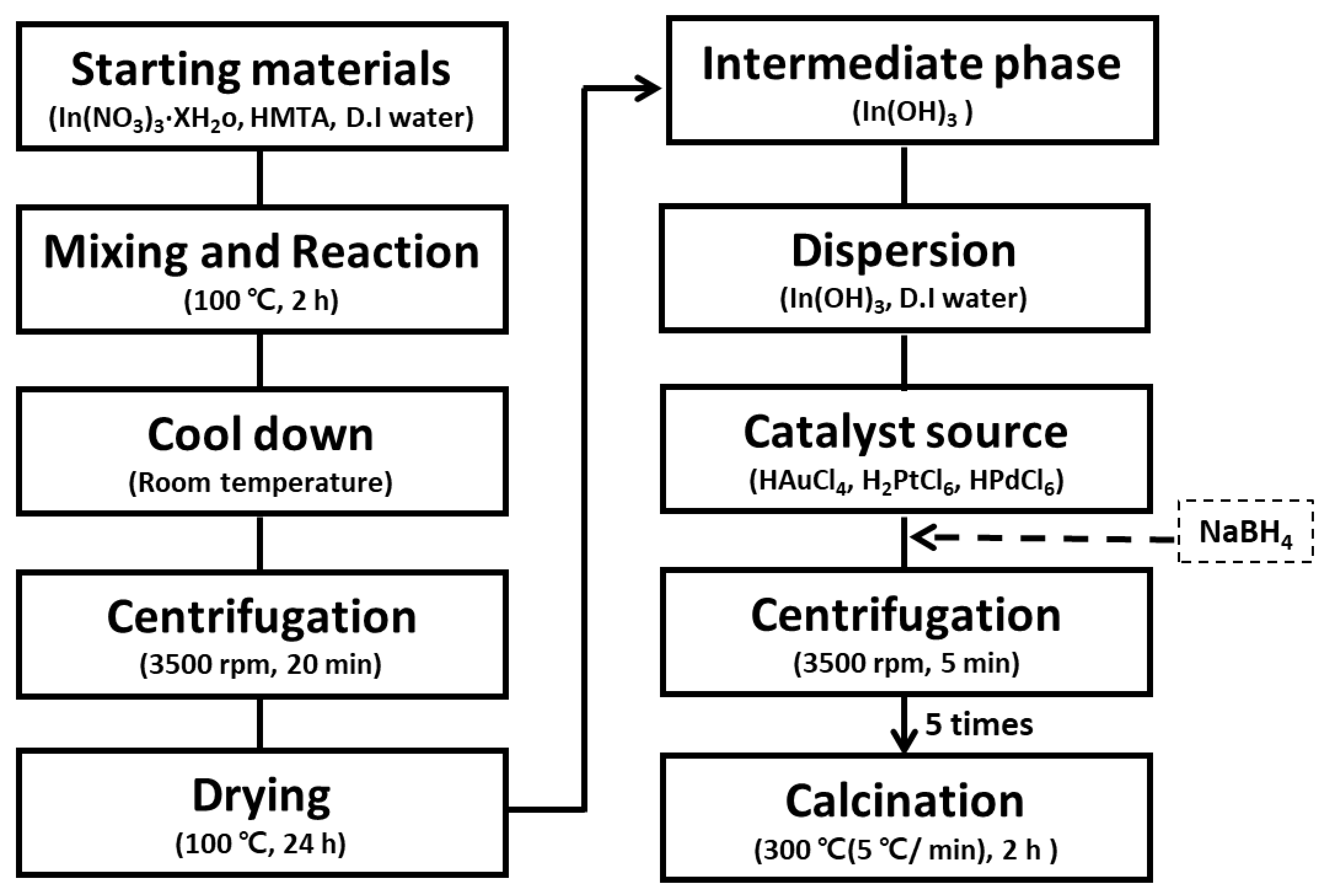
2.1. Preparation of Decorated In2O3 Particles (Au/In2O3, Pd/In2O3, Pt/In2O3)
All the chemical reagents for the synthesis of sensing materials were of analytical grade and used without further purification: indium (III) nitrate hydrate (In (NO3)3·xH2O) (Aldrich, 99.9%), HAuCl4 (Aldrich, 99.99%), and hexamethylenetetramine (Aldrich, 99%), NaBH4 (Aldrich, 98%) were used. The experiments were conducted according to the procedure presented in Figure 1. Catalyst-decorated In2O3 nanoparticles were synthesized by the thermal decomposition technique using reagents such as indium (III) nitrate hydrate InN3O3·6H2O, hexamethylenetetramine C6H2N4, sodium borohydride H4BNa, gold (III) chloride trihydrate HAuCl4·3H2O, chloroplatinic acid solution H2Cl6Pt, and palladium (II) chloride solution Cl2Pd, which were purchased from Sigma-Aldrich. A detailed experimental process of preparing catalyst-decorated indium oxide nanoparticles is shown in Figure 1. First, 1 mmol of indium (III) nitrate hydrate and 1 mmol of hexamethylenetetramine were added to 400 mL of distilled water and mixed. This mixed aqueous solution was heated to 100 °C and then maintained for 2 h with the solution refluxing. After the reaction was completed, the solution was cooled down to room temperature and then was centrifuged at 3500 rpm for 20 min, and finally dried at 100 °C for 24 h, which led to an intermediate phase, indium hydroxide powders In (OH)3. For dispersing the dried powder, 40 mL of distilled water was added to 0.2 g of the synthesized indium hydroxide, after 2 mL of 0.01 M HAuCl4·3H2O (Cl2Pd, H2Cl6Pt) was added to the dispersed solution, and 1 mL of 100 mm H4BNa was rapidly added as well. At the same time as the H4BNa was added, the solution turned reddish brown and was refrigerated for 2 h. Distilled water and ethanol were diluted and centrifuged 5 times. The sample with the catalyst was dried at 80 °C for 24 h. The dried samples were maintained at 300 °C (5/min) for 2 h and cooled to room temperature.
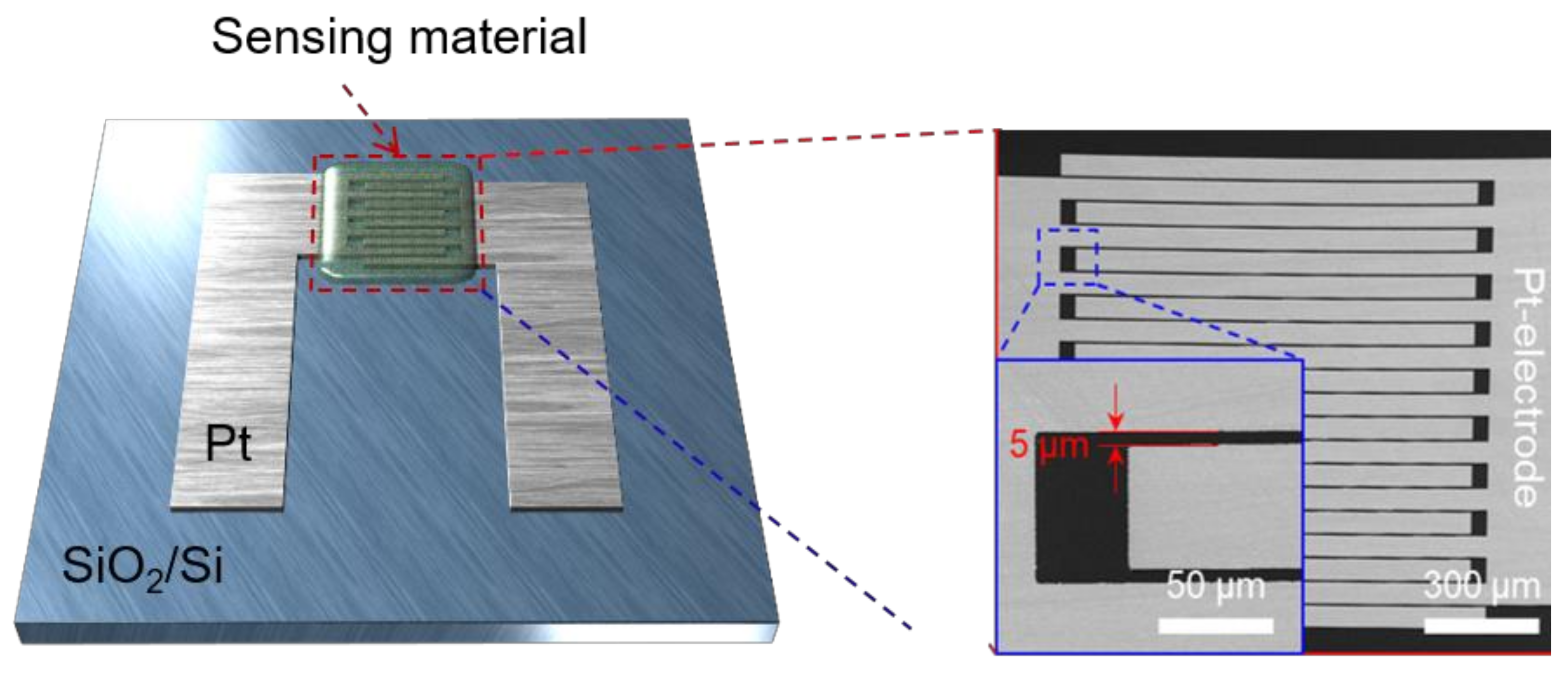
Figure 2 shows a schematic diagram of an In2O3 nanoparticles-based CO gas sensor and an Interdigital electrode (Interdigital Electrode) pattern, which was fabricated as follows. First, the sensing ink was prepared for application of the sensing material to the IDE pattern by gently sonicating it, and immersing 0.02 g In2O3-based sensing material in 4 mL D.I water for 2 h. Second, it was applied to the IDE substrate through an injection syringe and the drop position was accurately observed with an optical microscope. The In2O3 nanoparticle detection material was formed on the IDE substrate by injecting 0.1 L of ink drop per cycle and repeating drying.
2.2. Characterization
X-ray diffraction (XRD, Rigaku, D/2500VL/PC, (Cu Kα (λ = 1.5402 nm)) was used in order to confirm the crystal structure and crystallite size of the synthesized powder. Transmission electron microscopy (TEM, JEM-2100F, 200 kV, JEOL, Tokyo, Japan) was used to confirm the morphology and structure. STEM equipped with energy-dispersive X-ray spectroscopy (EDS) was used to analyze the surface morphology of the synthesized samples. The thickness and electrical resistance of the integrated sensing materials on the sensing part of IDE substrate were measured with the surface profiler (Veeco, Dektak 150) and multimeter (Keithley, model 2000). The gas sensing properties of In2O3 nanoparticles were measured in a hotplate. The gas flow was changed from dry air to CO gas (balanced with dry air) in a periodic manner. A constant flow rate of 500 sccm was used for the dry air and target gas. The reaction was accurately measured by measuring the reference resistance of dry air and the resistance fully saturated after exposure to the target gas.
3. Results
3.1. Structural and Morphological Characteristics
Figure 3 shows XRD patterns of intermediate phase In(OH)3 and In2O3 nanoparticles synthesized by the aforementioned thermal decomposition method, and were identified using JCPDS #160161 and JCPDS #060416, respectively. The diffraction patterns of both In(OH)3 and In2O3 nanoparticles were perfectly indexed to cubic structures. No impurity peak was observed; only sharp peaks existed, as shown in Figure 3. This means that the newly synthesized In2O3 nanoparticles had good crystallinity, where In2O3 nanoparticles were finally obtained by annealing the intermediate phase In(OH)3 at 300 °C.
The average crystallite size, D, was estimated using the Scherrer equation [38] as follows:
where β is the full width at half maximum (FWHM), Κ is the shape factor, and λ is the wavelength (Cu Kα = 1.54056 Å). The average crystal size of the In2O3 nanoparticles was ~10 nm in diameter, slightly smaller than what was observed (~15 nm) in the SEM and TEM images.
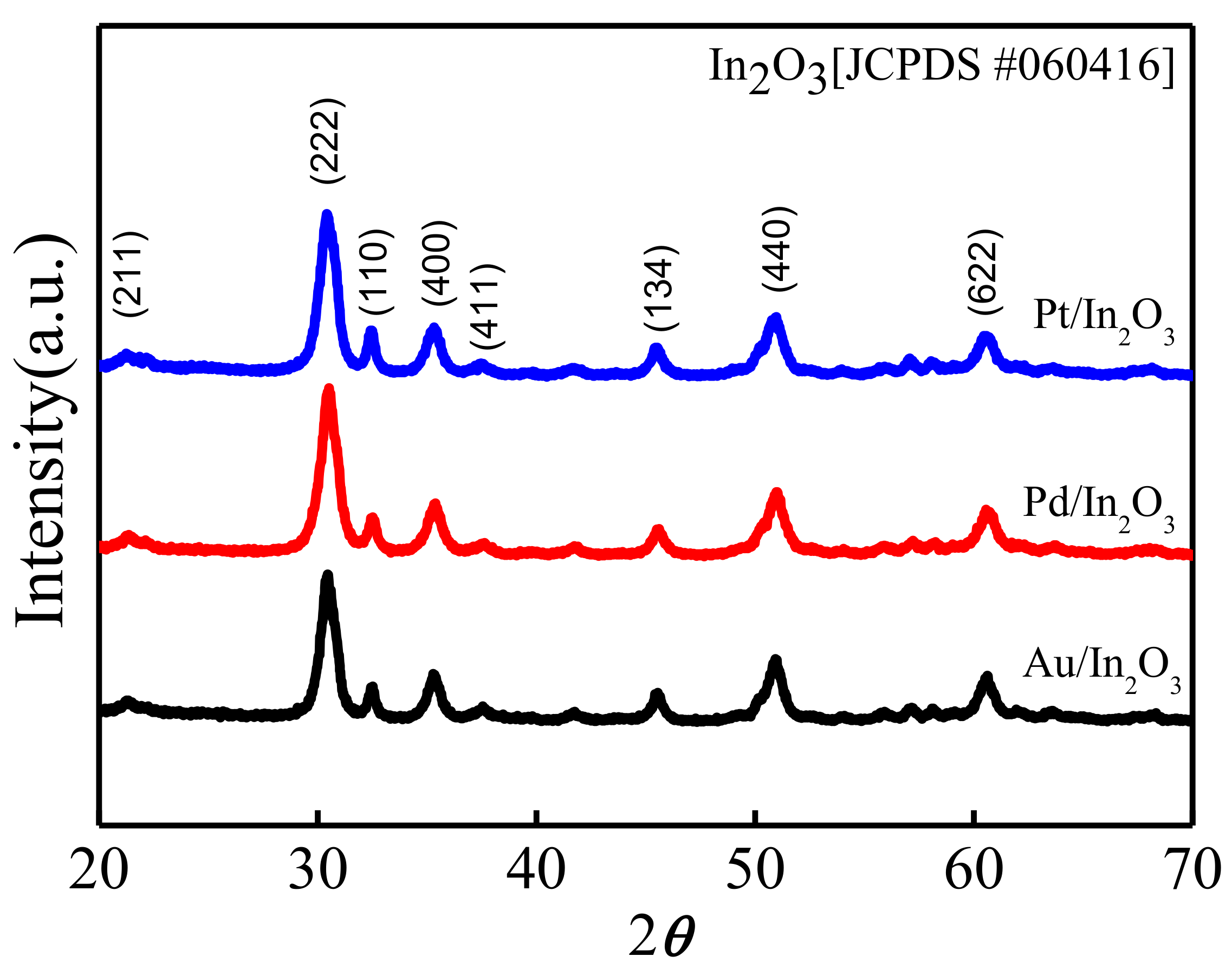
Figure 4 shows XRD patterns of catalyst-decorated In2O3 nanoparticles such as Au/In2O3, Pd/In2O3, and Pt/In2O3. The XRD patterns correspond to the cubic In2O3 crystal structure (JCPDS # 060416), but the lack of diffraction peaks from metallic catalysts of Au, Pd, and Pt likely means that the nanoparticles must be very small or amorphous due to the small amount of catalyst added to the In2O3 nanoparticles. A similar phenomenon was previously reported and was explained by the low content and small size of the catalysts [39]. Shifts of the XRD peaks did not seem to appear in the catalyst-decorated samples. Thus, it is considered that the added Au, Pd, and Pt were not incorporated into the In2O3 lattice, but rather were immobilized on the surfaces of In2O3 nanoparticles.
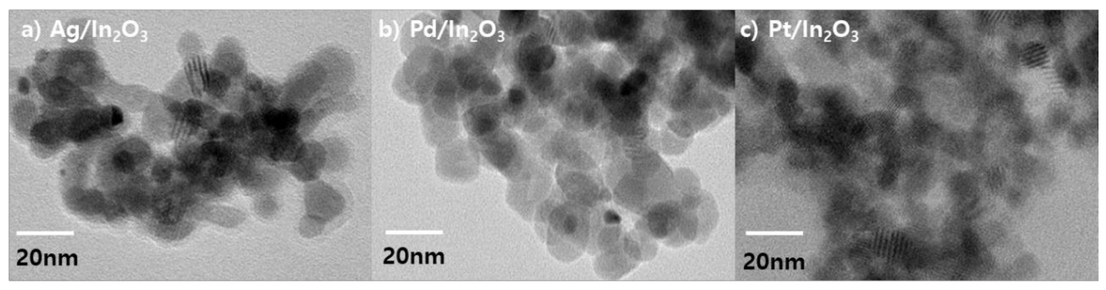
Figure 5a–c shows TEM images of Au/In2O3, Pd/In2O3, and Pd/In2O3 nanoparticles. Here, In2O3 nanoparticles have a slightly darker color with a diameter of 10 to 20 nm, whereas metal nanoparticles appear as dark colors with a diameter of 5 to 15 nm. The shape of the metal particles is more clearly displayed in the order of Au, Pd, and Pt particles, and the Pt particles appear blurry in the TEM images. The particle sizes of In2O3 and Au nanoparticles are estimated to be about 15 nm and 5 nm, respectively, as shown in Figure 5 (TEM image), where there is a lighter dark color for In2O3 particles and darker color for Au particles. Au particles are also shown as white particles in Figure 6 (HAADF image).
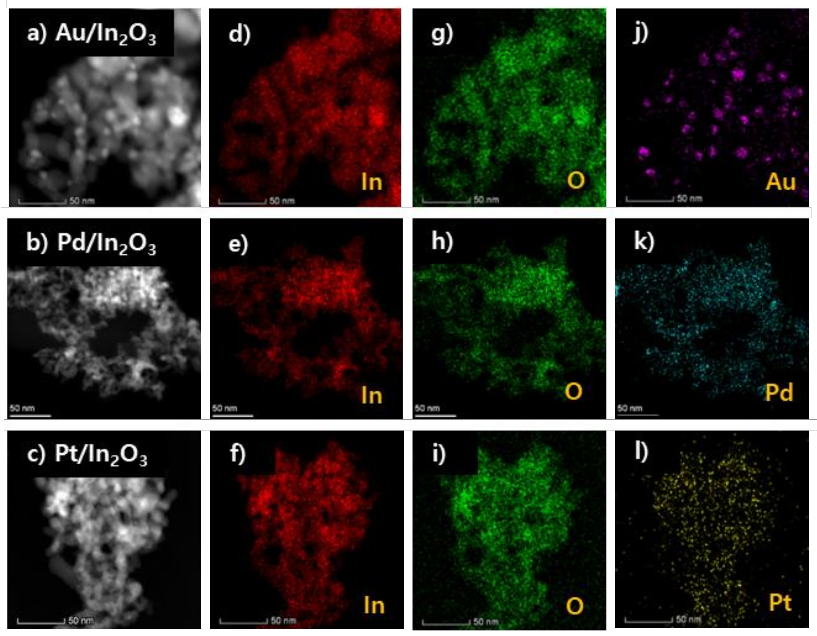
Figure 6a–c presents high-angle annular dark-field images (HAADF) of Au/In2O3, Pd/In2O3, and Pd/In2O3 nanoparticles. The Au nanoparticles are clearly indicated by white dots with a diameter of ~10 nm in Figure 6a, while Pd and Pt nanoparticles are also indicated by white dots, but with diameters of <5 nm and 5–10 nm, respectively. This is smaller than the Au nanoparticles shown in Figure 6b,c. HAADF is a STEM technique that produces an annular dark field image using very high angles, and incoherently scattered electrons. For elements with a higher atomic number, more electrons will scatter at higher angles due to the electrostatic interactions between the nuclear electron beams. Therefore, HAADF detectors detect larger signals from atoms with higher atomic numbers, making them appear brighter in the resulting image. Thus, HAADF is a useful way to easily identify elements with high atomic numbers in areas with elements of lower atomic numbers. In particular, it is adequate to determine the size of metal particles and their distribution in a heterogenous catalyst system. Figure 6d–l shows EDS elemental mapping images of In, O, Au, Pd, and Pt. This shows that metal catalysts were homogeneously distributed on the In2O3 particles, of which the condition is expected to play a great role in improving their gas sensing properties.
3.2. XPS Analysis of Noble Metal-Decorated In2O3 Particles
XPS is a surface-sensitive quantitative spectroscopic technique capable of identifying the overall electronic structure and density, chemical states, and electronic states of elements within a substance or that exist on its surface. In particular, XPS is a powerful measurement technique because it shows not only the elements present, but also other combined elements. A more detailed XPS spectrum was performed of Au/In2O3, Pd/In2O3, and Pt/In2O3 to reveal chemical bonding, and the results for the three particles were compared.
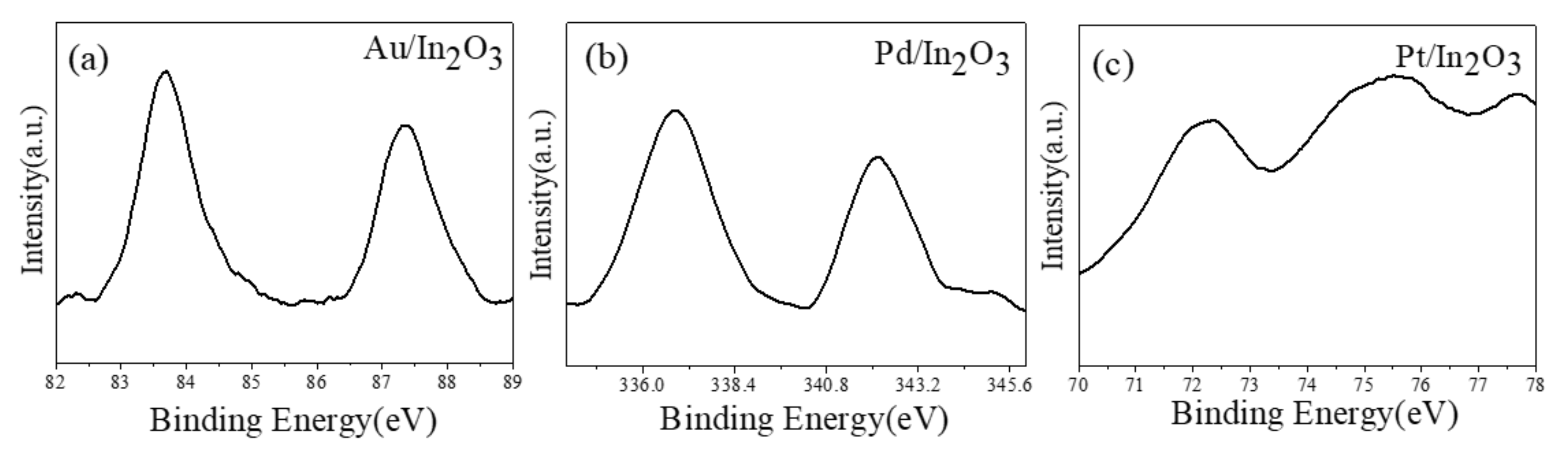
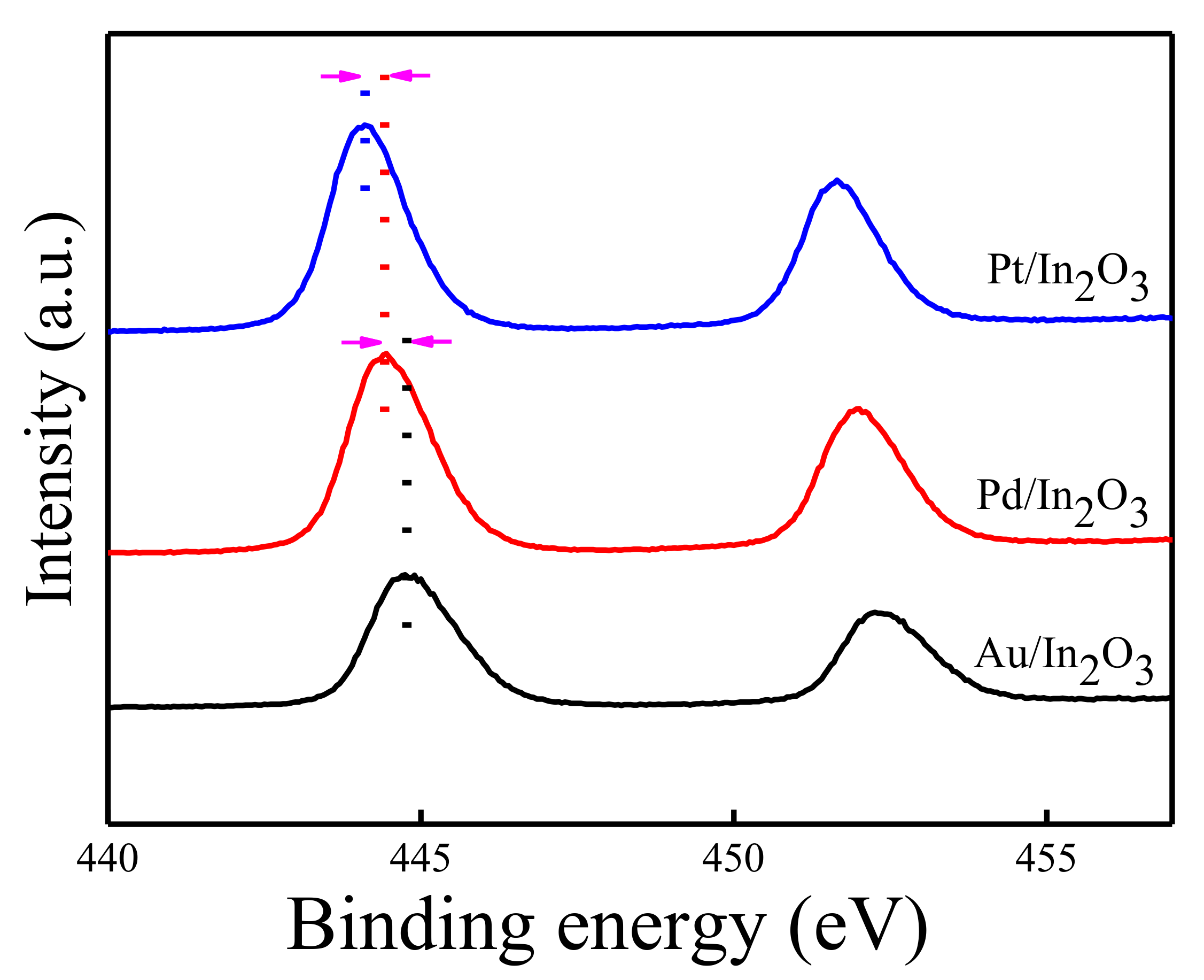
Figure 7a–c shows the XPS spectra of the metals Au, Pd, and Pt detected in Au/In2O3, Pd/In2O3, and Pt/In2O3 nanoparticles. Figure 7a shows that the high-resolution Au 4f core level spectrum is a dual property of Au/In2O3, with the peaks represented by metallic Au (Au0) centered at 83.7 and 87.4 eV, corresponding to 4f7/2 and 4f5/2. The Au 4f peak is relatively sharp and symmetrical, and Au/In2O3 represents the chemical state. According to the reference, the electron binding energies (BEs) of Au 4f7/2 and 4f5/2 are commonly 84.0 and 87.7 eV; in addition, the bulk metal Au was 86.4/90.1 eV for low-oxygen (Au+) oxidizing, and 85.5/89.2 eV for the high-oxygen species (Au3+) [40,41,42]. Compared with that of bulk metal Au, the 4f XPS spectrum of Au on Au/In2O3 showed a shift of 0.3 eV at low BE. The negative BE shift is usually due to strong interaction between the metal and In2O3 particles, where an electron transfers from In2O3 to Au. Compared to the Au 4f XPS peaks, the Pd 3d and Pt 4f XPS peaks are slightly wider, meaning that Pd/In2O3 or Pt/In2O3 has several chemical states of the metal, as shown in Figure 6 b,c. The Pd 3d peaks (Pd 3d5/2 and 3d3/2) correspond to 336.9 and 342.2 eV. However, these peaks do not correspond to any valence state of palladium (i.e., Pd0, Pd2+ (PdO), and Pd4+ (PdO2) with binding energies of 335.1/340.4 eV, 336.1/341.4 eV, and 337/343 eV [43]. Thus, the Pd particles are considered to coexist in the form of metal Pd, oxide PdO, and/or PdO2. The Pt 4f peaks are located at 72.4/75.5 eV, which correspond to Pt 4f7/2 and 4f5/2, respectively. These peaks can be interpreted as only Pd2+ (PdO) because they are nearly identical to the binding energy of Pt2+ (PtO) located at 72.2/75.5 eV, while the binding energy of metallic PtO is located at 71.4/74.6 eV [44] and is very different from PdO. Thus, it is considered that the Pt particles might exist in an oxide form of PtO. From the XPS results, the state of the In2O3 surface was different for Au, Pd, and Pt nanoparticles, and the degree of oxidation of the metal particles was in the order Au < Pd < Pt. Figure 8 exhibits the XPS spectra of In2O3 particles decorated with noble metals such as Au, Pd and Pt, where the peaks of the electrons are identified as In3d3/2 and In3d5/2. It is interesting to note that the peak positions of their 3d5/2 are shifted slightly toward the higher binding energy in the order Pt (444.1 eV), Pd (444.4 eV), and Au (444.8 eV), depending on the decorated-metal particles as compared to the metallic In3d5/2 peak of 443.7 eV or that of indium oxide (443.9 eV). The variation of peak positions in the XPS spectrum is due to the chemical status of the surface elements. Binding energies are determined by the electrostatic interaction between electrons and the nucleus; thus, the removal or addition of electronic charge as a result of changes in bonding will alter the shielding. If the nuclear charge is electrostatically shielded from all the other electrons in the atom (including valence electrons), the binding energy is reduced. Therefore, the removal of a valence electron charge, such as by oxidation, leads to lower electron density and increases the binding, while the addition of an electron charge leads to the higher electron density and decreases the binding energy.
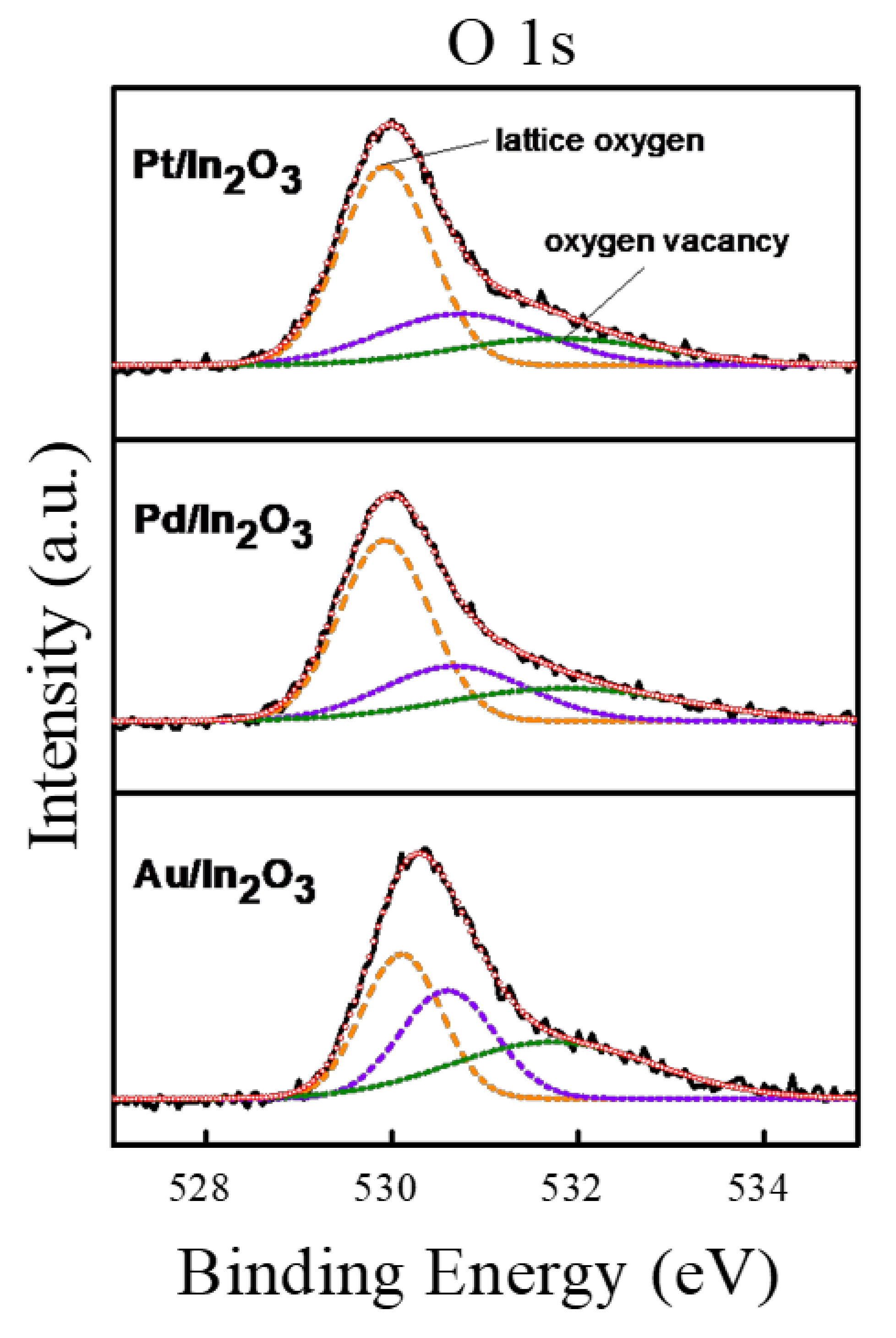
When noble metal-decorated In2O3 particles are exposed in air, oxygen is adsorbed to their surfaces and electrons from In2O3 particles are transferred to the surfaces of a noble metal or In2O3 particles, thereby generating depletion in the outer layer of In2O3. This means that the electron density in In2O3 particles is reduced. Therefore, considering the binding energy of the noble-metal decorated In2O3, Au-decorated In2O3 particles would have the largest depletion area free of electrons, followed by Pd-decorated In2O3 particles, and finally by Pt-decorated In2O3 particles. The thickness of the depletion layer is directly related to the sensitivity of a gas sensor based on a metal oxide semiconductor. Figure 9a–c shows the XPS spectra of oxygen (the O1s region) for Au/In2O3, Pd/In2O3, and Pt/In2O3 samples. The peaks can be deconvoluted by three Gaussian curves each. The three XPS peaks for Au/In2O3 are centered at 530.1, 530.6, and 531.9 eV; the peaks for Pd/In2O3 at 529.9, 530.7, and 532.1 eV; and the peaks for Pt/In2O3 at 529.9, 530.8, and 532.1 eV. If the lowest peaks can be assigned to the lattice oxygen (OI) in crystalline indium oxide, the middle peak could be associated with O2− ions (OII) in the oxygen vacancy region (deficient oxygen), and the highest peaks are due to oxygen. Chemical species (O2−, O−, or O2−) (OIII) are chemically adsorbed not only to the In2O3 surface, but also to the surfaces of hydroxy groups (-OH).
Deficient oxygen (OII) in the oxygen vacancy region and chemisorbed oxygen (OIII) species have significant effects on the sensing-reaction performance. Each oxygen vacancy provides two electrons and an active site for the adsorption of oxygen species [45]. An increase in the rate of oxygen deficiency promotes the adsorption of oxygen molecules on the surface of the sensing material, increasing the potential for interactions of In2O3 with the target gas, and thereby generating more active oxygen [46]. The peak areas caused by deficient oxygens were centered from 530.6 to 530.8, depending on the metal catalysts decorated, which could reflect the concentration of oxygen vacancies (defects) in the samples [45,47,48].
The relative percentages of lattice oxygen and oxygen vacancies for Au/In2O3, Pd/In2O3, and Pt/In2O3 particles are listed in Table 1. The relative percentage of oxygen vacancies is highest (65%) for Au/In2O3 particles, intermediate (49%) for Pd/In2O3 particles, and lowest (41%) for Pt/In2O3 particles. Thus, it is expected that the response to the target gas (carbon monoxide) would be more sensitive in the order Au/In2O3, Pd/In2O3, and Pt/In2O3, because more oxygen vacancies can create more active sites for chemisorption on the surface of In2O3 particles. The number of chemisorbed oxygen (OIII) species on metal/In2O3 particles is directly related to the depth of the electron depletion layer. Oxygens in air are chemically adsorbed to metal/In2O3 particles; therefore, electrons move from In2O3 to adsorbed oxygens, which creates an electron depletion layer on the surface of In2O3 [49,50]. The sensitivity to the target gas becomes greater in the order Au/In2O3, Pd/In2O3, and Pt/In2O3, because the number of adsorbed oxygens is greater in the same order, which creates the electron depletion layer.
3.3. Gas Sensing Properties
There is a modest temperature range for optimal adsorption and desorption, and they are largely influenced by the operating temperature. This affects the detection response of semiconductors and metal oxide gas sensors [51,52]. Sensors fabricated using pure In2O3, Au/In2O3, Pd/In2O3, and Pt/In2O3 nanoparticles were tested at 1, 5, 10, and 50 ppm CO gas concentrations in the 50 to 200 °C temperature range to find their optimum operating temperatures.
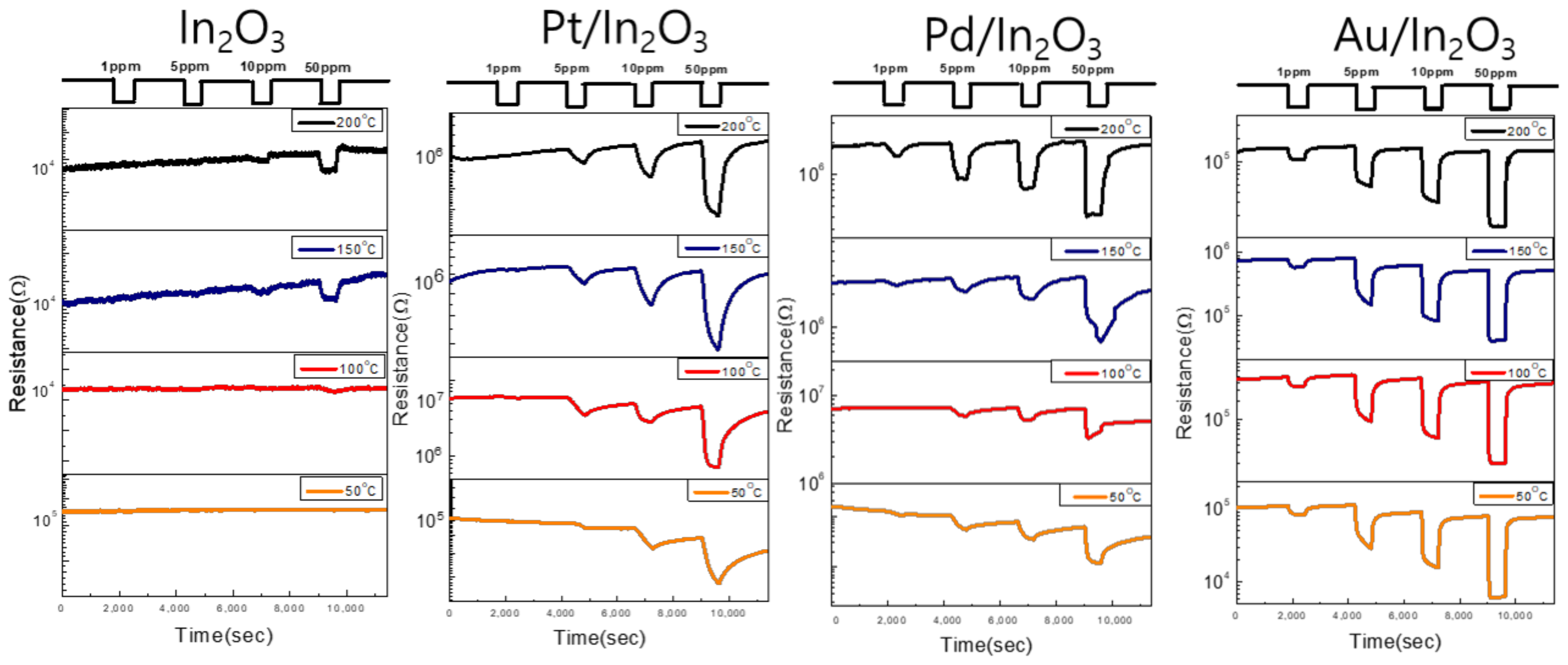
Figure 10 shows that the resistance of sensors degraded, as indicated by the downward drift of the resistance over time, whose trends were especially distinct for the Pt/In2O3 and Pd/ In2O3 at 50 °C. The sensing characteristics of MOS (metal semiconductor) gas sensors depend on various parameters such as sensing material, operating temperature, humidity, and target gas type, etc. Operating temperature is an important parameter for gas sensor materials because it has a significant influence on the occurrence of surface reactions during gas detection. When the gas sensor in the measuring chamber is exposed to dry air at a fixed temperature, oxygen molecules are adsorbed on the gas sensor surface, increasing its resistance. Looking at the XPS spectrum results, the density of oxygen molecules adsorbed on the gas sensor will increase in the order of Pd/ In2O3, Pt/ In2O3, and Au/In2O3 according to the sensing material. Even though a small amount of humidity exists in the measuring chamber, water molecules will move to the surface area of the gas sensor that lacks adsorbed oxygen ions, reducing its resistance. Therefore, because the desorption of water molecules is more difficult at lower temperatures than at higher temperatures, at lower operating temperatures, the decrease in resistance of the gas sensor over time can be greater in the order of Au/ In2O3, Pt/ In2O3 and Pd/ In2O3.
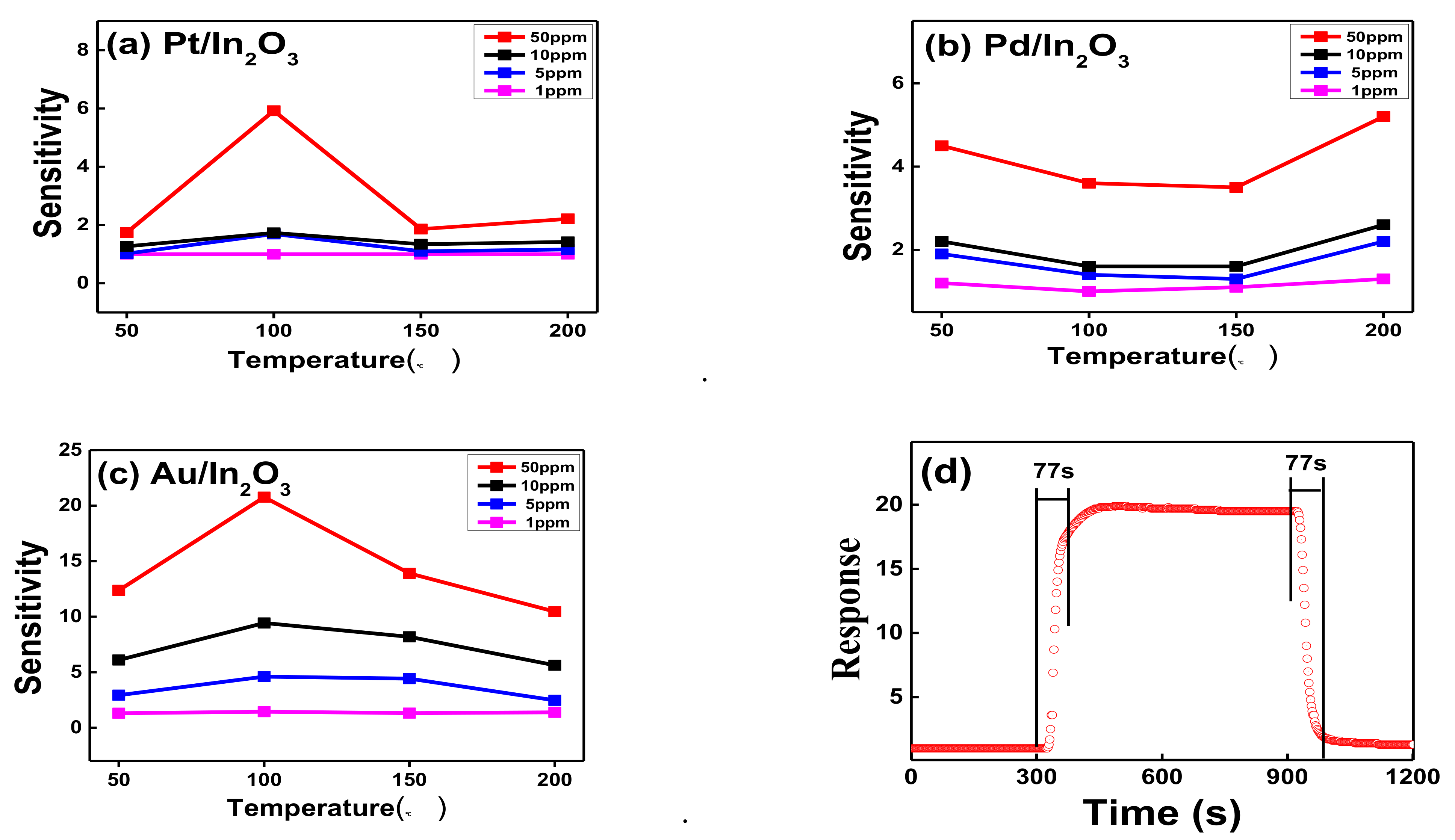
Figure 11a–c shows the sensitivities of the Pt/In2O3, Pd/In2O3, and Au/In2O3 gas sensors as a function of temperature at various CO gas concentrations (also presented in Table 2). It was clearly shown that the sensitivity continuously increases with increases in the CO gas concentration. CO poisoning, which is worse due to the easier oxidation of Pt nanoparticles than other particles, seems to have a bad influence on the detection characteristics such as the response and recovery time of the Pt/In2O3 sensor, as shown in Figure 10b. However, the sensitivities of the Pd/In2O3 and Au/In2O3 gas sensors revealed different trends, not only monotonically increasing, but also showing their highest sensitivities at 100 °C, with increasing sensing temperature. Unlike the above, the sensitivity of Pt/In2O3 had its lowest value at temperatures between 100 and 150 °C. The Au/In2O3 gas sensor had maximum sensitivities of 1.44, 5.54, 8.92, and 19.88 in relation to the CO gas concentrations of 1, 5, 10 and 50 ppm, respectively, at 100 °C. This appears to be superior to the results from previous studies [53,54]. Figure 11d shows the response and recovery times of Au/In2O3 at a 50 ppm CO concentration at the optimal temperature of 100 °C, and it can be seen that the response and recovery time are the same (77 s). The response and recovery time are considered two of the major factors for evaluating gas sensor performance. The response time of the sensor is defined as the time it takes to reach 90% of its saturation limit after exposure to CO gas, and the recovery time is defined as the time required for the sensor to reach 10% of its original resistance.
3.4. Gas Sensing Mechanism
As a rule, semiconducting metal oxide-based sensors work by the adsorption and desorption of gas molecules to and from the oxide surface, which leads to change of the sensor electrical resistance. When a sensing material such as In2O3 is exposed to air, O2 molecules in the air are adsorbed to the surface. This holds electrons from the oxides carried to form highly chemisorbed oxygen species (O2−, O− or O2−) [55,56], as indicated in Equations (1)–(4) due to the strong electron affinity of O2. The activation temperature decides the present form of oxygen ions. Commonly, O2− requires a higher activation temperature to be chemisorbed, while the other two ions appear at lower temperatures. In particular, O− was the predominant oxygen species adsorbed at 150–400 °C [57].
O2(gas) → O2(ads)
O2(ads) + e− → O−2(ads)
O−2(ads) + e− → 2O−(ads)
O−(ads) + e− → O2− (ads)
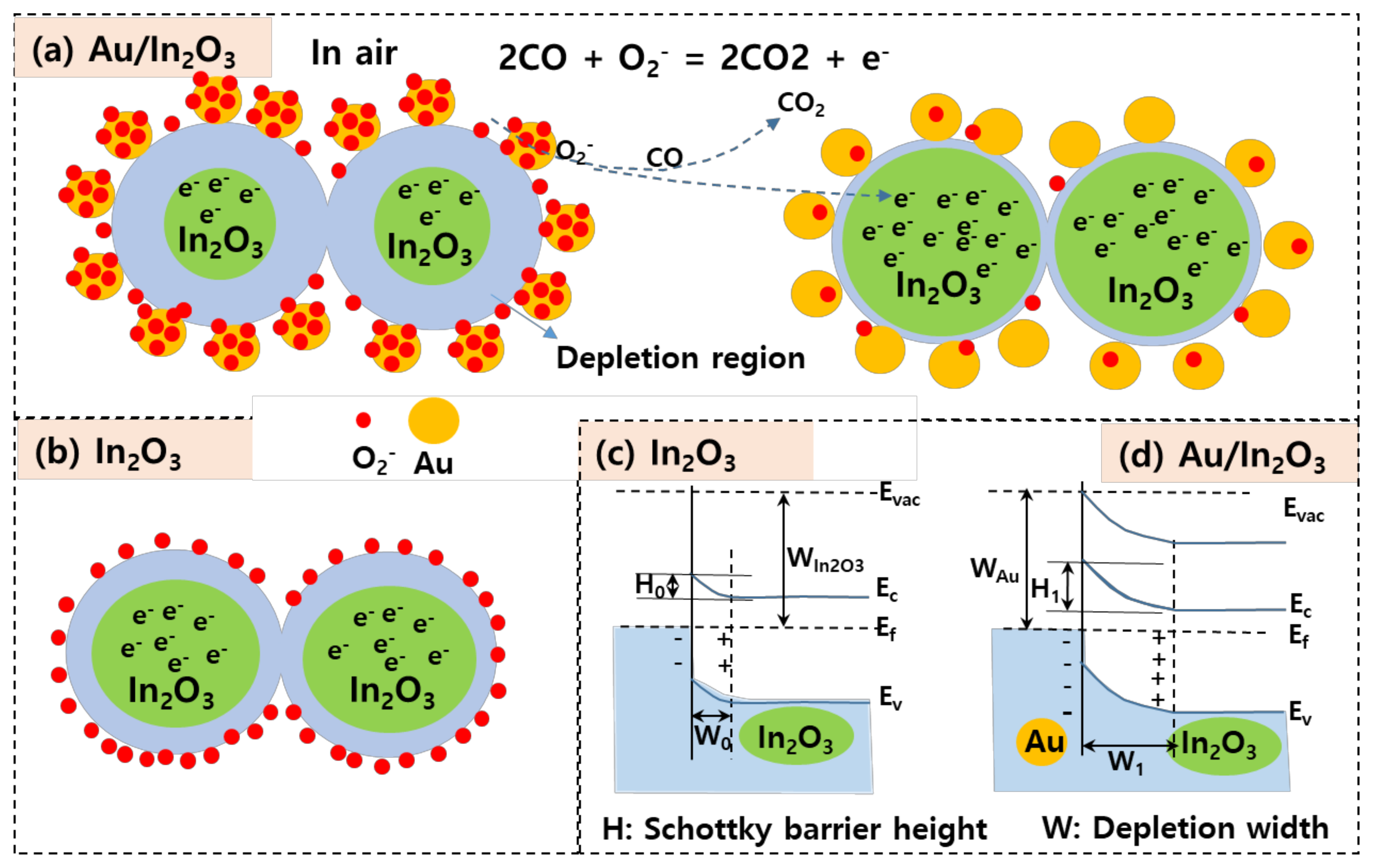
Due to the relatively small band gap of a semiconducting oxide gas sensor, electrons can be thermally excited from the valence band and/or the donor levels to the unoccupied conduction band in the operating temperature from about 50 to 500 °C, which is needed to overcome the activation energy barrier of surface redox reactions and also increase the electron concentration in the conduction band. If a gas sensor sample is gradually heated, electrons will be thermally activated to the conduction band. If these excited electrons in the conduction band of In2O3 semiconductor move from In2O3 particle to oxygen molecule (O2) absorbed on the surface of In2O3 particles inducing chemisorbed oxygen species (O2−, O− or O2−), electron depletion layers will be created beneath the In2O3 oxide surface, as schematically shown in Figure 12b,c.
The electron depletion layer works as a potential barrier between neighboring grains, so that the sensor resistance increases in air. When a reducing gas such as carbon monoxide (CO) was released into the test chamber, the oxygen species adsorbed to the oxide surface reacted with CO gas, as indicated in Equations (5) and (6). The electrons caught by oxygen species are released back into the conduction band of In2O3, so that depletion layer thickness becomes thinner, causing a remarkable decrease in resistance of the gas sensor.
2CO + O−2(ads) → 2CO2 + e−
CO + O−(ads) → CO2 + e−
The sensing performance of oxide sensors such as In2O3 was essentially determined by changes in the thickness of the electron depletion layer as the atmosphere changed. One way to improve sensor sensitivity was to decorate the In2O3 surface with metal nanoparticles. This made the change in depth of the electron depletion layer more sensitive, which magnified the change in the resistance of In2O3 sensors.
Using Au, Pd, or Pt nanoparticles with photosensitizers to decorate the In2O3 surface can trigger two sensitization mechanisms. One mechanism is the electronic sensitization caused by interfacial electronic redistribution, and the other mechanism is the chemical sensitization caused by surface atom transport [55,56,57]. In the electron sensitivity process, electrons are products of In2O3 particles, and due to the difference in work function, they move to the precious metal nanoparticles. Thereby, the precious metal nanoparticles become rich in electrons, resulting in an increase in the electron depletion layer. An In2O3 sensor decorated with noble metal will become more sensitive to change in the external atmosphere because the potential barrier height between neighboring grains rises. Chemical sensitization of noble metals occurs by the transport of atoms in the interfacial region, known as the spillover effect, and has been used to describe the catalytic process of metal-supported catalysts [24,25,26]. In this process, the loaded metal particles such as Pt, Pd and Au will have more active sites than In2O3 particles for the adsorption of molecular oxygen and target gas (carbon monoxide). This will lead to much more adsorption and easier dissociation of these molecules owing to the high catalytic or conductive nature of the noble metal particles. In air, chemically adsorbed ionic oxygen species on the metal particles will move toward the In2O3 particles, causing the enlarged depletion region near the outer surface region of the In2O3 particles. In the target gas atmosphere, the target gas is easily adsorbed to these metal nanoparticles and is rapidly oxidized by ionic oxygen species densely present near the metal nanoparticles. This spillover effect of metal nanoparticles may significantly improve the number and speed of electron transfer, which is directly related to the sensitivity and response speed of the gas sensor.
The effectiveness of noble metals depends greatly on their location and chemical state. As revealed in XPS analysis, Au nanoparticles decorating In2O3 particles exist mainly as metal Au0 and exhibit much stronger electronic interactions with In2O3 particles than with Pd or Pt. This means that the sensing properties of Au/In2O3 for CO gas are superior to those of pristine In2O3, Pd/In2O3, and Pt/In2O3, because Pd or Pt nanoparticles decorating In2O3 are partially oxidized or exist in the form of oxides. Oxidation of Pd or Pt particles reduces the effective active area of metal Pd or Pt particles for gas adsorption, weakening the electron interaction between the metal and In2O3, and greatly affecting the spillover of the target gas to the metal nanoparticle surface. In addition to the chemical state, the amount and dispersion of noble metal nanoparticles decorating the In2O3 surface have a great influence on the sensitization effect of a sensor’s sensing properties [25,57].
To identify the effects of noble metals on In2O3 sensors, the responses of Pt/In2O3, Pd/In2O3, and Au/In2O3 sensors with CO gas were compare, as shown in Figure 12a–d. The response of the four In2O3-based sensors to carbon monoxide (CO) followed the order Au/In2O3 > Pd/In2O3 > Pt/In2O3 > In2O3. This means that Au/In2O3 is better than Pd/In2O3 and Pt/In2O3, and that this is directly related to the catalytic activity of Au nanoparticles. Nanoparticles are well known because their catalytic functions can serve as effective adsorption sites that bind oxygen molecules. Thus, more of the absorbed oxygen species diffuse to the surface of the sensing material, resulting in a thick layer of electron depletion layers forming a conduction band of In2O3. Due to its high coverage of chemically active oxygen species, the Au/In2O3 sensor reacts more sensitively to CO gas, directly generating high sensitivity. The strong electronic interaction between Au and In2O3 particles resulted in the formation of a typical metal–semiconductor junction near the interface, as shown in Figure 12a,d. The working function of Au (5.1 eV) is greater than that of In2O3 (4.8 eV); therefore, electrons are transferred to the conduction band of Au on the In2O3 particles. Thus, the energy band of In2O3 exhibits greater flexion on the Au/In2O3 interface than the energy loss in the pure In2O3 nanoparticle electron depletion layer as the resistance increases. More electrons are trapped in the conduction band, and due to the movement of In2O3, changes in the electron concentration of CO gas finally lead to a clear change in resistance. Therefore, sensors based on the Au/In2O3 sensor have higher gas response than Pd/In2O3, Pt/In2O3, and In2O3. In decorated In2O3 sensors, the sensitivity effect of metal nanoparticles is mainly determined by their chemical state, and the decoration with Au is considered to have a significant acceleration effect on their sensitivity to CO gas. Pt/In2O3 had the lowest response rate to CO gas among the three sensors (except for bare In2O3).
4. Conclusions
In2O3-based gas sensors decorated with three noble metals (Au, Pd, and Pt) to detect carbon monoxide at temperatures near room temperature were fabricated and investigated using XRD, TEM, and XPS. Their sensing properties were measured with specifically designed sensing equipment. It should be noted that Au/In2O3 nanoparticles exhibited far better sensing responses to CO gas at low temperature (50 °C) than Pd/In2O3 or Pt/In2O3. The sensitizing effect of noble metals on the sensing properties of CO gas sensors was explained by the surface chemical state of Au, Pd, and Pt nanoparticles and their interaction with the In2O3 particles. The concentration of oxygen vacancies in the In2O3 lattice depends on which catalyst is used to decorate the surfaces of In2O3 particles, and it has been shown that the degree of oxidation of the metal particles has a great influence on their detection characteristics. The average crystal size of In2O3 nanoparticles obtained by Scherr’s equation was about 10 nm (diameter), which is slightly smaller than the diameter observed in SEM and TEM images (~15 nm). The Au-decorated In2O3 sensor exhibited superior sensitivity to CO gas at 100 °C, with sensitivity and response times of 1.44 and 77 s, respectively, compared to other Pd- or Pt-decorated In2O3 sensors. This can be explained by two factors. One seems to be the high concentration of oxygen adsorbed on the surface of In2O3 particles due to the high concentration of oxygen vacancies in the In2O3 lattice. Another factor is the improvement in activity due to pure metallic Au particles that are not oxidized, unlike catalysts with Pt or Pd, which become partially or fully oxidized.
Author Contributions
Conceptualization, M.C.; methodology, J.H. validation, M.C, H.J., D.-S.K., D.S.K.; formal analysis, D.S.K., H.-S.S.; investigation, H.-S.S.; writing—original draft preparation M.C.; writing—review and editing, B.-K.J. and M.C. All authors have read and agreed to the published version of the manuscript.
Funding
This work was supported by the Core Technology (20181110200170, Development of Removal of Acid Gas and Fine Particle for Coal Thermal Power Plant). This work was supported by the Ministry of Trade, Industry & Energy, and supported by the Basic Science Research Program through the National Research Foundation of Korea (NRF) funded by the Ministry of Education (No.2018R1A6A1A03026005).
Institutional Review Board Statement
Not applicable.
Informed Consent Statement
Not applicable.
Data Availability Statement
Not applicable.
Conflicts of Interest
The authors declare no conflict of interest.
References
- McCue, J.T.; Ying, J.Y. SnO2-In2O3 nanocomposites as semiconductor gas sensors for CO and NOx etection. Chem. Mater. 2007, 19, 1009–1015. [Google Scholar] [CrossRef]
- Goto, T.; Itoh, T.; Akamatsu, T.; Izu, N.; Shin, W. CO sensing properties of Au/SnO2–Co3O4 catalysts on a micro thermoelectric gas sensor. Sens. Actuators B Chem. 2016, 223, 774–783. [Google Scholar] [CrossRef]
- Bhardwaj, N.; Pandey, A.; Satpati, B.; Tomar, M.; Gupta, V.; Mohapatra, S. Enhanced CO gas sensing properties of Cu doped SnO2 nanostructures prepared by a facile wet chemical method. Phys. Chem. Chem. Phys. 2016, 18, 18846–18854. [Google Scholar] [CrossRef]
- Kumar, A.; Sanger, A.; Kumar, A.; Chandra, R. Highly sensitive and selective CO gas sensor based on hydrophobic SnO2/CuO bilayer. RSC Adv. 2016, 6, 47178–47184. [Google Scholar] [CrossRef]
- Tee, T.S.; Hui, T.C.; Yi, C.W.; Chin, Y.C.; Umar, A.A.; Titian, G.R.; Beng, L.H.K.; Sing, L.K.; Yahaya, M.; Salleh, M.M. Microwave-assisted hydrolysis preparation of highly crystalline ZnO nanorod array for room temperature photoluminescence-based CO gas sensor. Sens. Actuators B Chem. 2016, 227, 304–312. [Google Scholar]
- Barsan, N.; Simion, C.; Heine, T.; Pokhrel, S.; Weimer, U. Modeling of sensing and transduction for p-type semiconducting metal oxide based gas sensors. J. Electroceram. 2010, 25, 11–19. [Google Scholar] [CrossRef]
- Lee, J.S.; Ha, T.J.; Hong, M.H.; Park, C.S.; Park, H.H. The effect of multiwalled carbon nanotube doping on the CO gas sensitivity of TiO2 xerogel composite film. Appl. Surf. Sci. 2013, 269, 125–128. [Google Scholar] [CrossRef]
- Hjiri, M.; El Mir, L.; Leonardi, S.G.; Pistone, A.; Mavilia, L.; Neri, G. Al-doped ZnO for highly sensitive CO gas sensors. Sens. Actuators B Chem. 2014, 196, 413–420. [Google Scholar] [CrossRef]
- Fu, H.; Hou, C.; Gu, F.; Han, D.; Wang, Z. Facile preparation of rod-like Au/In2O3 nanocomposites exhibiting high response to CO at room temperature. Sens. Actuators B Chem. 2017, 243, 516–524. [Google Scholar] [CrossRef]
- Hübner, M.; Simion, C.E.; Haensch, A.; Barsan, N.; Weimar, U. CO sensing mechanism with WO3 based gas sensors. Sens. Actuators B Chem. 2010, 151, 103–106. [Google Scholar] [CrossRef]
- Patil, D.; Patil, P.; Subramanian, V.; Joy, P.A.; Potdar, H.S. Highly sensitive and fast responding CO sensor based on Co3O4 nanorods. Talanta 2010, 81, 37–43. [Google Scholar] [CrossRef] [PubMed]
- Steinhauer, S.; Brunet, E.; Maier, T.; Mutinati, G.C.; Köck, A.; Köck, A. CuO nanowire gas sensors for CO detection in humid atmosphere. In Proceedings of the 2013 Transducers & Eurosensors XXVII: The 17th International Conference on Solid-State Sensors, Actuators and Microsystems, Barcelona, Spain, 16–20 June 2013; pp. 1095–1098. [Google Scholar]
- Batzill, M.; Diebold, U. The surface and materials science of tin oxide. Prog. Surf. Sci. 2005, 79, 47–154. [Google Scholar] [CrossRef]
- Moos, R.; Sahner, K.; Fleischer, M.; Guth, U. Solid State Gas Sensor Research in Germany—A Status Report. Sensors 2009, 9, 4323–4365. [Google Scholar] [CrossRef] [PubMed]
- Rumyantseva, M.N.; Gas’kov, A.M. Chemical Modification of Nanocrystalline Metal Oxides: Effect of the Real Structure and Surface Chemistry on the Sensor Properties. Russ. Chem. Bull. 2008, 57, 1106–1125. [Google Scholar] [CrossRef]
- Lee, J.H. Gas Sensors Using Hierarchical and Hollow Oxide Nanostructures: Overview. Sens. Actuators B Chem. 2009, 140, 319–336. [Google Scholar] [CrossRef]
- Noguchi, S.; Sakata, H. Electrical properties of undoped In2O3 films prepared by reactive evaporation. J. Phys. D Appl. Phys. 1980, 13, 1129–1133. [Google Scholar] [CrossRef]
- Shigesato, Y.; Takaki, S.; Haranoh, T. Electrical and structural properties of low resistivity tin-doped indium oxide films. J. Appl. Phys. 1992, 71, 3356–3364. [Google Scholar] [CrossRef]
- Shanmugasundaram, A.; Basak, P.; Satyanarayana, L.; Manorama, S.V. Hierarchical SnO/SnO2 nanocomposites: Formation of in situ p–n junctions and enhanced H2 sensing. Sens. Actuators B Chem. 2013, 185, 265–273. [Google Scholar] [CrossRef]
- Kawasaki, H.; Ueda, T.; Suda, Y.; Ohshima, T. Properties of metal doped tungsten oxide thin films for NOx gas sensors grown by PLD method combined with sputtering process. Sens. Actuators B Chem. 2004, 100, 266–269. [Google Scholar] [CrossRef]
- Hieua, N.V.; Thuy, L.T.B.; Chien, N.D. Highly sensitive thin film NH3 gas sensor operating at room temperature based on SnO2/MWCNTs composite. Sens. Actuators B Chem. 2008, 129, 888–895. [Google Scholar] [CrossRef]
- Lin, Q.; Li, Y.; Yang, M. Tin oxide/graphene composite fabricated via a hydrothermal method for gas sensors working at room temperature. Sens. Actuators B Chem. 2012, 173, 139–147. [Google Scholar] [CrossRef]
- Liu, X.; Zhang, J.; Guo, X.; Wu, S.; Wang, S. Amino acid-assisted one-pot assembly of Au, Pt nanoparticles onto one-dimensional ZnO microrods. Nanoscale 2010, 2, 1178–1184. [Google Scholar] [CrossRef]
- Gogurla, N.; Sinha, A.K.; Santra, S.; Manna, S.; Ray, S.K. Multifunctional Au-ZnO plasmonic nanostructures for enhanced UV photodetector and room temperature NO sensing devices. Sci. Rep. 2014, 4, 6483. [Google Scholar] [CrossRef] [Green Version]
- Santra, S.; Guha, P.K.; Ali, S.Z.; Hiralal, P.; Unalan, H.E.; Covington, J.A.; Amaratunga, G.A.J.; Milne, W.I.; Gardner, J.W.; Udrea, F. ZnO nanowires grown on SOI CMOS substrate for ethanol sensing. Sens. Actuators B Chem. 2010, 146, 559–565. [Google Scholar] [CrossRef]
- Phani, A.R.; Manorama, S.V.; Rao, V.J. X-ray photoelectron spectroscopy studies on Pd doped SnO2 liquid petroleum gas sensor. Appl. Phys. Lett. 1997, 71, 2358–2360. [Google Scholar] [CrossRef]
- Zhang, J.; Liu, X.H.; Guo, X.Z.; Wu, S.H.; Wang, S.R. A general approach to fabricate diverse noble-metal (Au, Pt Ag, Pt/Au)/Fe2O3 hybrid nanomaterials. Chem. Eur. J. 2010, 16, 8108–8116. [Google Scholar] [CrossRef] [PubMed]
- Kolmakov, A.; Klenov, D.O.; Lilach, Y.; Stemmer, S.; Moskovits, M. Enhanced gas sensing by individual SnO2 nanowires and nanobelts functionalized with Pd Catalyst Particles. Nano Lett. 2005, 5, 667–673. [Google Scholar] [CrossRef] [PubMed]
- Vander Wal, R.L.; Hunter, G.W.; Xu, J.C.; Kulis, M.J.; Berger, G.M.; Ticich, T.M. Metal-oxide nanostructure and gas-sensing performance. Sens. Actuators B Chem. 2009, 138, 113–119. [Google Scholar] [CrossRef]
- Joshi, R.K.; Hu, Q.; Alvi, F.; Joshi, N.; Kumar, A. Au decorated zinc oxide nanowires for CO sensing. J. Phys. Chem. C. 2009, 113, 16199–16202. [Google Scholar] [CrossRef]
- Romanovskaya, V.; Ivanovskaya, M.; Bogdanov, P. A study of sensing properties of Pt- and Au-loaded In2O3 ceramics. Sens. Actuators B Chem 1999, 56, 31–36. [Google Scholar] [CrossRef]
- Shen, Y.; Yamazaki, T.; Liu, Z.; Meng, D.; Kikuta, T. Hydrogen sensors made of undoped and Pt-doped SnO2 nanowires. J. Alloys Compd. 2009, 488, 21–25. [Google Scholar] [CrossRef]
- Han, X.G.; Jin, M.S.; Xie, S.F.; Kuang, Q.; Jiang, Z.Y.; Jiang, Y.Q.; Xie, Z.X.; Zheng, L.; Angew, S. Synthesis of trapezohedral indium oxide nanoparticles with high-index {211} facets and high gas sensing activity. Chem. Int. Ed. 2009, 48, 9180–91832009. [Google Scholar] [CrossRef] [PubMed]
- Wang, X.; Han, X.G.; Xie, S.F.; Kuang, Q.; Jiang, Y.Q.; Zhang, S.B.; Mu, X.L.; Chen, X.G.; Xie, Z.X.; Zheng, L.S. Controlled synthesis and enhanced catalytic and gas-sensing properties of tin dioxide nanoparticles with exposed high-energy facets. Chem. Eur. J. 2012, 18, 2283–2289. [Google Scholar] [CrossRef] [PubMed]
- Valden, M.; Pak, S.; Lai, X.; Goodman, D.W. Structure sensitivity of CO oxidation over model Au/TiO2 2 catalysts. Catal. Lett. 1998, 56, 7–10. [Google Scholar] [CrossRef]
- Schubert, M.M.; Hackenberg, S.; Veen, A.C.V.; Muhler, M.; Plzak, V.; Behm, R.J. CO Oxidation over Supported Gold Catalysts—“Inert” and “Active” Support Materials and Their Role for the Oxygen Supply. J. Catal. 2001, 197, 113–122. [Google Scholar] [CrossRef]
- Grunwaldt, J.D.; Bailker, A. Gold/Titania Interfaces and Their Role in Carbon Monoxide Oxidation. Phys. Chem. B 1999, 103, 1002–1012. [Google Scholar] [CrossRef]
- Liu, H.; Kozlov, A.I.; Kozlov, A.P.; Shido, T.; Asakura, K. Iwasawa, Active Oxygen Species and Mechanism for LowTemperature CO Oxidation Reaction on a TiO2-Supported Au Catalyst Prepared from Au(PPh3)(NO3) and As-Precipitated Titanium Hydroxide. J. Catal. 1999, 185, 252–264. [Google Scholar] [CrossRef]
- Guggenheim, S.; Bain, D.C.; Bergaya, F.; Brigatti, M.F.; Drits, V.A.; Eberl, D.D.; Formoso, M.L.L.; Galán, E.; Merriman, R.J.; Peacor, D.E. Report of the Association Internationale pour l’Etude des Argiles (AIPEA) Nomenclature Committee for 2001: Order, disorder and crystallinity in phyllosilicates and the use of the ‘Crystallinity Index’. Clay Miner. 2002, 37, 389–393. [Google Scholar] [CrossRef]
- Sun, Y.; Zhuang, L.; Lu, J.; Hong, X.; Liu, P. Collapse in Crystalline Structure and Decline in Catalytic Activity of Pt Nanoparticles on Reducing Particle Size to 1nm. J. Am. Chem. Soc. 2007, 129, 15465–15467. [Google Scholar] [CrossRef]
- Jaramillo, T.F.; Baeck, S.H.; Cuenya, B.R.; McFarland, E.W. Catalytic Activity of Supported Au Nanoparticles Deposited from Block Copolymer Micelles. J. Am. Chem. Soc. 2003, 125, 7148–7149. [Google Scholar] [CrossRef] [PubMed]
- Kim, K.J.; Kreider, P.B.; Chang, C.H.; Park, C.M.; Ahn, H.G. Visible-light-sensitive nanoscale Au-ZnO photocatalysts. J. Nanopart. Res. 2013, 42, 1–11. [Google Scholar] [CrossRef]
- Minicò, S.; Scirè, S.; Crisafulli, C.; Galvagno, S. Influence of catalyst pretreatments on volatile organic compounds oxidation over gold/iron oxide. Appl. Catal. B Environ. 2001, 34, 277–285. [Google Scholar] [CrossRef]
- Yang, D.J.; Kamienchick, I.; Youn, D.Y.; Rothschild, A.; Kim, I.D. Ultrasensitive and Highly Selective Gas Sensors Based on Electrospun SnO2 Nanofibers Modified by Pd Loading. Adv. Funct. Mater. 2010, 20, 4258–4264. [Google Scholar] [CrossRef]
- Liu, J.; Chen, G.; Yu, Y.; Wu, Y.; Zhou, M.; Zhang, H.; Lv, C.; Zheng, Y.; He, F. Controllable synthesis of In2O3 octodecahedra exposing {110} facets with enhanced gas sensing performance. RSC Adv. 2015, 5, 44306–44312. [Google Scholar] [CrossRef]
- Zhang, Y.; Yueying, L.; Linsheng, Z.; Deye, L.; Fengmin, L.; Fangmeng, L.; Xishuang, L.; Xu, Y.; Yuan, G.; Geyu, L. The role of Ce doping in enhancing sensing performance of ZnO-based gas sensor by adjusting the proportion of oxygen species. Sens. Actuators B Chem. 2018, 273, 991–998. [Google Scholar] [CrossRef]
- Lei, F.; Sun, Y.; Liu, K.; Gao, S.; Liang, L.; Pan, B.; Xie, Y. Oxygen vacancies confined in ultrathin indium oxide porous sheets for promoted visible-light water splitting. J. Am. Chem. Soc. 2014, 136, 6826–6829. [Google Scholar] [CrossRef]
- Gan, J.; Lu, X.; Wu, J.; Xie, S.; Zhai, T.; Yu, M.; Zhang, Z.; Mao, Y.; Wang, S.C.I.; Shen, Y.; et al. Oxygen vacancies promoting photoelectrochemical performance of In2O3 nanocubes. Sci. Rep. 2013, 3, 1021. [Google Scholar] [CrossRef] [PubMed] [Green Version]
- Liu, C.; Kuang, Q.; Xie, Z.X.; Zheng, L.S. The effect of noble metal (Au, Pd and Pt) nanoparticles on the gas sensing performance of SnO2-based sensors: A case study on the {221} high-index faceted SnO2 octahedra. CrystEngComm 2015, 17, 6308–6313. [Google Scholar] [CrossRef]
- Ma, N.; Suematsu, K.; Yuasa, M.; Kida, T.; Shimanoe, K. Effect of water vapor on Pd-loaded SnO2 nanoparticles gas sensor. ACS Appl. Mater. Interfaces 2015, 7, 5863–5869. [Google Scholar] [CrossRef] [PubMed]
- Xiang, Q.; Meng, G.F.; Zhao, H.B.; Zhang, Y.; Li, H.; Ma, W.J.; Xu, J.Q. Au nanoparticle modified WO3 nanorods with their enhanced properties for photocatalysis and gas Sensing. J. Phys. Chem. C 2010, 114, 2049–2055. [Google Scholar] [CrossRef]
- Gong, H.; Hu, J.Q.; Wang, J.H.; Ong, C.H.; Zhu, F.R. Nano-crystalline Cu-doped ZnO thin film gas sensor for CO. Sens. Actuators B Chem. 2006, 115, 247–251. [Google Scholar] [CrossRef]
- Wei, S.; Yu, Y.; Zhou, M. CO gas sensing of Pd-doped ZnO nanofibers synthesized by electrospinning method. Mater. Lett. 2010, 64, 2284–2286. [Google Scholar] [CrossRef]
- Hubner, M.; Koziej, D.; Grunwaldt, J.D.; Weimar, U.; Barsan, N. An Au clusters related spill-over sensitization mechanism in SnO2-based gas sensors identified by operando HERFD-XAS, work function changes, DC resistance and catalytic conversion studies. Phys. Chem. Chem. Phys. 2012, 14, 13249–13254. [Google Scholar] [CrossRef] [PubMed]
- Fu, Q.; Wagner, T. Interaction of nanostructured metal overlayers with oxide surfaces. Surf. Sci. Rep. 2007, 62, 431–498. [Google Scholar] [CrossRef]
- Li, X.; Feng, W.; Xiao, Y.; Sun, P.; Hu, X.; Shimanoe, K.; Lu, G.; Yamazoe, N. Hollow Zinc oxide microspheres functionalized by Au nanoparticles for gas sensors. RSC Adv. 2014, 4, 28005–28010. [Google Scholar] [CrossRef]
- Min, B.K.; Friend, C.M. Heterogeneous Gold-Based Catalysis for Green Chemistry:Low-Temperature CO Oxidation and Propene Oxidation. Chem. Rev. 2007, 107, 2709–2724. [Google Scholar] [CrossRef] [PubMed]
Figure 1.
Experimental procedure for synthesizing In2O3 nanoparticles.

Figure 2.
Schematic diagram of In2O3 nanoparticles-based CO gas sensor and Interdigital electrode (IDE).
Figure 2.
Schematic diagram of In2O3 nanoparticles-based CO gas sensor and Interdigital electrode (IDE).

Figure 3.
X-ray diffraction patterns of intermediate phase In(OH)3 and In2O3 nanoparticles.

Figure 4.
XRD patterns of catalyst-decorated In2O3 nanoparticles Au/In2O3, Pd/In2O3 and Pt/In2O3.

Figure 5.
TEM images of (a) Au/In2O3, (b) Pd/In2O3, (c) Pt/In2O3 nanoparticles.

Figure 6.
HAADF images of Au/In2O3, Pd/In2O3 and Pt/In2O3 nanoparticles (a–c) and their EDS elemental mapping images (d–l).
Figure 6.
HAADF images of Au/In2O3, Pd/In2O3 and Pt/In2O3 nanoparticles (a–c) and their EDS elemental mapping images (d–l).

Figure 7.
(a–c) XPS spectra of metallic Au, Pd and Pt detected from the In2O3/Au, In2O3/Pd and In2O3/Pt particles, respectively.
Figure 7.
(a–c) XPS spectra of metallic Au, Pd and Pt detected from the In2O3/Au, In2O3/Pd and In2O3/Pt particles, respectively.

Figure 8.
XPS spectra of In2O3 particles decorated with noble metals such as Au, Pd and Pt, where the peaks of the electrons are identified as In3d3/2 and In3d5/2.
Figure 8.
XPS spectra of In2O3 particles decorated with noble metals such as Au, Pd and Pt, where the peaks of the electrons are identified as In3d3/2 and In3d5/2.

Figure 9.
XPS spectra of oxygen in O1s region for Au/In2O3, Pd/In2O3 and Pt/In2O3 samples, where the peaks can be deconvoluted into three Gaussian curves, respectively.
Figure 9.
XPS spectra of oxygen in O1s region for Au/In2O3, Pd/In2O3 and Pt/In2O3 samples, where the peaks can be deconvoluted into three Gaussian curves, respectively.

Figure 10.
The response versus various concentrations of the Au, Pd and Pt-decorated In2O3 CO gas sensor for 1–50 ppm from left to right are bare In2O3; Pt/In2O3; Pd/In2O3 and Au/In2O3 nanoparticles.
Figure 10.
The response versus various concentrations of the Au, Pd and Pt-decorated In2O3 CO gas sensor for 1–50 ppm from left to right are bare In2O3; Pt/In2O3; Pd/In2O3 and Au/In2O3 nanoparticles.

Figure 11.
(a–c) Sensitivity of the In2O3 nanoparticles sensor as a function of CO concentration and temperature, and (d) is the response and recovery time of Au/In2O3 at 50 ppm CO concentration at the optimal temperature of 100 °C.
Figure 11.
(a–c) Sensitivity of the In2O3 nanoparticles sensor as a function of CO concentration and temperature, and (d) is the response and recovery time of Au/In2O3 at 50 ppm CO concentration at the optimal temperature of 100 °C.

Figure 12.
(a,b) Schematic illustration of gas sensing mechanism and (c,d) schematic energy band diagram of the sensing materials (In2O3, Au/In2O3).
Figure 12.
(a,b) Schematic illustration of gas sensing mechanism and (c,d) schematic energy band diagram of the sensing materials (In2O3, Au/In2O3).


Table 1.
The relative percentages of lattice oxygen and oxygen vacancies for Au/In2O3, Pd/In2O3, and Pt/In2O3 particles.
Table 1.
The relative percentages of lattice oxygen and oxygen vacancies for Au/In2O3, Pd/In2O3, and Pt/In2O3 particles.
| Gas Sensors | OI (Lattice Oxygen) | OII (Oxygen Vacancy) | ||
|---|---|---|---|---|
| Peak (eV) | Percentage (%) | Peak (eV) | Percentage (%) | |
| Au/In2O3 | 530.1 | 35 | 530.6 | 65 |
| Pd/In2O3 | 529.9 | 51 | 530.7 | 49 |
| Pt/In2O3 | 529.9 | 56 | 530.8 | 44 |
Table 2.
Sensing responses of Pt/In2O3, Pd/In2O3, Au/In2O3 sensors to CO gas as a function of CO gas concentration and temperature.
Table 2.
Sensing responses of Pt/In2O3, Pd/In2O3, Au/In2O3 sensors to CO gas as a function of CO gas concentration and temperature.
| ppm | Pt/In2O3 | Pd/In2O3 | Au/In2O3 | ||||||||||
|---|---|---|---|---|---|---|---|---|---|---|---|---|---|
| °C | 1 | 5 | 10 | 50 | 1 | 5 | 10 | 50 | 1 | 5 | 10 | 50 | |
| 50 | 1.00 | 1.06 | 1.07 | 1.75 | 1.2 | 1.9 | 2.20 | 4.5 | 1.31 | 3.87 | 5.59 | 11.49 | |
| 100 | 1.00 | 1.67 | 1.72 | 6.09 | 1.0 | 1.4 | 1.60 | 3.6 | 1.44 | 5.54 | 8.92 | 19.88 | |
| 150 | 1.00 | 1.14 | 1.34 | 1.88 | 1.1 | 1.3 | 1.60 | 3.5 | 1.32 | 5.36 | 7.68 | 13.02 | |
| 200 | 1.00 | 1.16 | 1.41 | 2.24 | 1.3 | 2.2 | 2.60 | 5.2 | 1.39 | 3.41 | 5.12 | 9.58 | |
Publisher’s Note: MDPI stays neutral with regard to jurisdictional claims in published maps and institutional affiliations. |
© 2021 by the authors. Licensee MDPI, Basel, Switzerland. This article is an open access article distributed under the terms and conditions of the Creative Commons Attribution (CC BY) license (https://creativecommons.org/licenses/by/4.0/).
Share and Cite
MDPI and ACS Style
Hwang, J.; Jung, H.; Shin, H.-S.; Kim, D.-S.; Kim, D.S.; Ju, B.-K.; Chun, M. The Effect of Noble Metals on Co Gas Sensing Properties of In2O3 Nanoparticles. Appl. Sci. 2021, 11, 4903. https://doi.org/10.3390/app11114903
AMA Style
Hwang J, Jung H, Shin H-S, Kim D-S, Kim DS, Ju B-K, Chun M. The Effect of Noble Metals on Co Gas Sensing Properties of In2O3 Nanoparticles. Applied Sciences. 2021; 11(11):4903. https://doi.org/10.3390/app11114903
Chicago/Turabian StyleHwang, JinAh, Hyunsung Jung, Hyo-Soon Shin, Dae-Sung Kim, Dong Soo Kim, Byeong-Kwon Ju, and MyoungPyo Chun. 2021. "The Effect of Noble Metals on Co Gas Sensing Properties of In2O3 Nanoparticles" Applied Sciences 11, no. 11: 4903. https://doi.org/10.3390/app11114903
Note that from the first issue of 2016, this journal uses article numbers instead of page numbers. See further details here.