
Analysis of Inductive Displacement Sensors with Large Range and Nanoscale Resolution

1
College of Intelligence Science and Technology, National University of Defense Technology, Changsha 410000, China
2
HUST-Wuxi Research Institute, Wuxi 214174, China
*
Author to whom correspondence should be addressed.
Appl. Sci. 2021, 11(21), 10134; https://doi.org/10.3390/app112110134
Submission received: 24 June 2021
/
Revised: 28 September 2021
/
Accepted: 15 October 2021
/
Published: 28 October 2021
(This article belongs to the Special Issue New Trends in the Control of Robots and Mechatronic Systems)
Abstract
:With the advantages of high resolution, structural simplicity, reliability, compact size, and high sensitivity, inductive sensors have been widely used in nanopositioning systems. However, the measuring range of traditional inductive sensors are usually limited to 0.2 mm. A novel analysis and design methodology of the miniaturized inductive sensor with large measuring range and nanoscale resolution is proposed. Firstly, an accurate leakage inductance model is established. Secondly, a design rule of armature size is proposed by considering the fringing effect. Then, the error terms introduced by the measurement circuit of differential inductive sensors are analyzed and the corresponding error suppression methods are illustrated. Moreover, A design rule of selecting the optimal excitation frequency is proposed to meet the requirements of high Q value and high bandwidth, and to minimize the impact of core loss resistance on the performance of the sensor. Validated by the experiments, the proposed analysis and design method can effectively guide the design of the miniaturized inductive sensor with nanoscale resolution in the measuring range of ±0.5 mm. The overall size of the fabricated sensor prototypes is less than 6 mm × 6 mm × 3 mm. Combined with large range, high resolution and ideal miniaturization, this inductive sensor can be well suitable for compact and large stroke nanopositioning systems.
1. Introduction
The nanometer displacement sensor is an important part of the nanopositioning system, which provides feedback signal for the motion control and greatly affects the performance of the system [1,2,3]. There are six main requirements for displacement sensors in the nanopositioning applications of our interest: (1) Nanoscale resolution (0.1~10 nm); (2) Large measuring range (for example, hundreds of microns or even few millimeters); (3) Miniaturization (for example, the size of each of the three coordinate directions is several microns); (4) High bandwidth; (5) Immunity to harsh environments; (6) Multi-degree-of- freedom measurement can be realized by configuring multiple sensors in different positions.
The most commonly used measurement methods that can potentially meet the above conditions are capacitive, eddy current and inductive sensors [4]. Among these types of sensors, capacitive sensors have the highest resolution. However, the dielectric between capacitive plates is sensitive to environmental conditions, which makes capacitive sensors unsuitable for harsh environments. The eddy current sensor is one of the most common position sensors in nanopositioning systems because of its high resolution and immunity to environmental changes, as well as super-high bandwidth of tens of kHz. One possible drawback of eddy current sensor is that it is easy to be disturbed by external magnetic field. There are many types of inductive sensors, of which the two most commonly used inductance techniques for nanoscale measurement are linear variable differential transformers (LVDTs) and linear variable differential inductors (LVDIs) [5]. LVDTs are sensitive to lateral motion, thus not suited to multi-degree-of-freedom applications [4]. Generally, LVDTs are defined independently, and they are distinguished from the inductive sensors we will analysis below in this paper. Compared with LVDTs, LVDIs are more suitable for the nanopositioning applications of our interest. In some literature [6,7], LVDIs are also referred to as variable reluctance transducers/sensors, in the following the appearance of “inductive sensor” all refer to this type of sensors. Further discussion of such inductive sensors will be carried out below.
Inductive sensors have been introduced in a review [5], which states that such sensors (with total dimensions of around 5 mm × 5 mm × 5 mm) can reach a range of 0.2 mm with a signal-to-noise ratio of about 10,000:1 and achieve a resolution better than 50 pm RMS in the range of 50~100 nm. This indicates that the inductive sensor has ultra-high resolution and compactness required by nanopositioning applications. In early 1980s, Velayudhan et al. [8] described a simple scheme for the continuous measurement of displacement using the differential inductive sensor and its application in reaction torque measurement of a rotating machine delivering or receiving power. Their prototype instrument can reach a resolution of about 80 nm RMS for the measuring range of ±0.1 mm. In recent 10 years, inductive sensors are still concerned by researchers. Noel Philip et al. [7] have proposed a simple, and high accuracy dual slope inductance-to-digital converter (DSIDC) suitable for differential inductive sensors. This converter not only provides a direct digital output, but also improves the linear range of operation significantly. Wang Kun et al. [9] have studied the differential inductive sensor for application in the position detection of the active magnetic bearing (AMB). They designed an inductive sensor that has higher linearity, higher sensitivity and wider bandwidth than traditional inductive displacement sensors and the suspension accuracy of the magnetic suspension molecular pump can reach 2.4 μm when applying this sensor.
It is difficult to simultaneously satisfy the miniaturized, large measuring range, nanoscale resolution for displacement sensors. The above displacement sensors (capacitive sensors, eddy current sensors, LVDTs and inductive sensors) are inevitably facing the problem of small range when miniaturization and nanoscale resolution are required, so they need to be improved or be replaced with better alternatives to adapt to the compact and large stroke multi-degree-of-freedom nanopositioning systems. Typical commercial products corresponding to these sensors are shown in Table 1, in which the sensor probe diameter must be less than ∅10 mm. It is desired that the sensor probe be as small as possible and meet large range and nanoscale resolution requirements. The inductive sensors (LVDIs) of our interest are difficult to be found corresponding commercial products in the market, but they can be smaller in size than the advanced products shown in the table. However, from the current literatures [5,8], the measuring range of the inductive sensor meeting the requirements of miniaturization and nanoscale resolution has not exceeded 0.2 mm. This is because of the significant nonlinearity of inductive sensors operating in large range. If the range of inductive sensors can be extended on the basis of miniaturization, such sensors may be more competitive than the commercial displacement sensors listed in Table 1. With the development of modern digital linearization techniques, such as polynomial compensation by software, good original linearity is not so important in many situations, thus the range of inductive sensors can be extended by using the nonlinearity characteristic. On this basis, a reliable design method of large range inductive sensors is needed. It is necessary to analyze the inductance vs. measured displacement characteristic and the measuring circuit factors of inductive sensors, comprehensively consider the effects of leakage inductance, fringing effect and core loss, and select the appropriate excitation frequency. The size of the sensor core and the number of coil turns should also be considered. In this way, the error source can be suppressed to the greatest extent and the good performance of the inductive sensor in a large range of operation can well be guaranteed.
In this paper, in order to obtain an appropriate design method and ensure the large range operation performance of the inductive sensor with miniaturized size, extensive analysis is carried out by analytical analysis, finite element method and experiments. This paper is organized as follows: Section 2 discusses the structure of inductive sensors and its current performance limitations. Consequently, a novel leakage inductance model of inductive sensors is established by using FEM in Section 3. By considering the fringing effect, the influence of armature size on the inductance of inductive sensors is studied, and the design rule of armature size is established. The important role of Q value in suppress the complex error terms of differential inductive sensors and improving their performance for large range operation is analyzed. In Section 4, based on the requirements of high Q value and high bandwidth, the corresponding design rule is formulated, and the selection method of the optimal excitation frequency is proposed. The content of Section 5 is the experimental results of the prototype sensors to support the research of analysis and design methods in this paper. In Section 6, the conclusion is made.
2. Structure of Inductive Sensors
Inductive sensors are mainly composed of sensor core (sensor probe), armature and coil, as shown in Figure 1. Both core and armature are made of magnetically permeable materials with high permeability. When the air gap length (δ) between the armature and sensor probe changes, the reluctance in the air gap changes, so as the inductance of the sensor. By measuring the change of inductance (L), the displacement of the armature can be obtained.
Inductive sensors usually adopt differential measurement mode with a pair of two electronically matched sensor probes, which are positioned on opposite sides or ends of the armature for displacement measurement. The advantages of this approach are improved sensitivity and linearity of the transfer characteristic, improved immunity to environmental changes, and a simplified electronic interface. The structure of differential inductive sensors is shown in Figure 2. The sensor probe to armature relationship is such that as the armature moves toward to one sensor probe, it moves away from the other an equal amount. As a result, the inductance of one probe increases and the other one decreases.
Differential inductive sensors are commonly used for measuring small displacement for their high precision. However, there will be great nonlinearity if they are operated in a large range. We define the armature displacement as x, and the armature displacement at the center of the two probes is zero. ∆L = L1 − L2 is defined as the differential inductance. Figure 3 shows ∆L vs. x nonlinear relationship of the differential inductive sensor operated in large range. The curve can be divided into 3 zones:
- (1)
- Zone1: Linear workspace zone in differential working mode;
- (2)
- Zone2: Nonlinear workspace zone in differential working mode;
- (3)
- Zone3: Nonlinear workspace zone in single-probe-dominated mode.
When the displacement to be measured is in a small range within the Zone1, the inductive sensor is working in the ideal differential mode with high linearity. As the displacement increases to Zone2, the nonlinearity increases. As further displacement increases, the inductance value of one probe away from the armature decreases to a very small value. The differential effect is weakened. The working mode of the inductive sensor in Zone3 changes into a single-probe-dominated mode.
There are several difficulties in the design of inductive sensors with large range and high precision:
- (1)
- The inaccurate traditional calculation model of inductance vs. displacement characteristic can not meet the design requirements of large range inductive sensors;
- (2)
- In terms of circuit factors, there are complex error terms present in the transfer characteristic of differential inductive sensors;
- (3)
- Due to the existence of core loss, it is difficult to effectively improve the Q value;
- (4)
- There is a lack of a design rule to select the optimal excitation frequency for the inductive sensor.
3. Principle Analysis
3.1. Traditional Analytical Model and Its Limitations
The change of the air gap (δ) between the armature and the sensor probe leads to the change of the inductance of the inductive sensor, which is based on the principle of electromagnetic induction. The traditional inductance calculation model [9] is given by,
where N is coil turns of the inductive sensor and Rm is the reluctance of the air gap, which is given by,
where μ0 is the vacuum permeability; δ is the air gap length between sensor probe and armature; S is the cross-sectional area of the core. Substituting (2) into (1), yields,
For the differential inductive sensor shown in Figure 2, the differential inductance (∆L) is given by,
where L1 and L2 are the inductance values of a pair of probes with differential arrangement, respectively. According to Equation (3), ∆L can be equivalent to,
where δ0 is zero gap, Δδ is the armature displacement x, and L0 is the zero position inductance when the armature is located in the center between two probes. L0 can be obtained from Equation (3), that is,
when using the above model to design a large range inductive sensor, there are at least the following two limitations:
- (1)
- Ignoring the leakage inductance, the total inductance of the inductive sensor under different air gap cannot be estimated correctly, resulting in large deviation in the design of parameters of the sensor;
- (2)
- The fringing effect are not considered. When a large range differential inductive sensor is used to measure the armature displacement with transverse parasitic motion, the above model cannot guide the design of the armature size.
3.2. Finite Element Analysis and High-Precision Modeling of Leakage Inductance
The finite element model of the inductive sensor is established by using COMSOL Multiphysics, as shown in Figure 4. The inductance vs. air gap characteristic of the inductive sensor can be accurately calculated by finite element method (FEM).
To analyze the leakage inductance, it is necessary to know the distribution of the leakage flux. It is clearly illuminated in Figure 4 that the leakage flux is mainly concentrated in the slot between the two legs of the sensor probe, as well as the outer side of the leg. The flux density at several points (m0, m1, m2, m3, m4, c0, c1) are obtained by FEM, as Figure 5 shows.
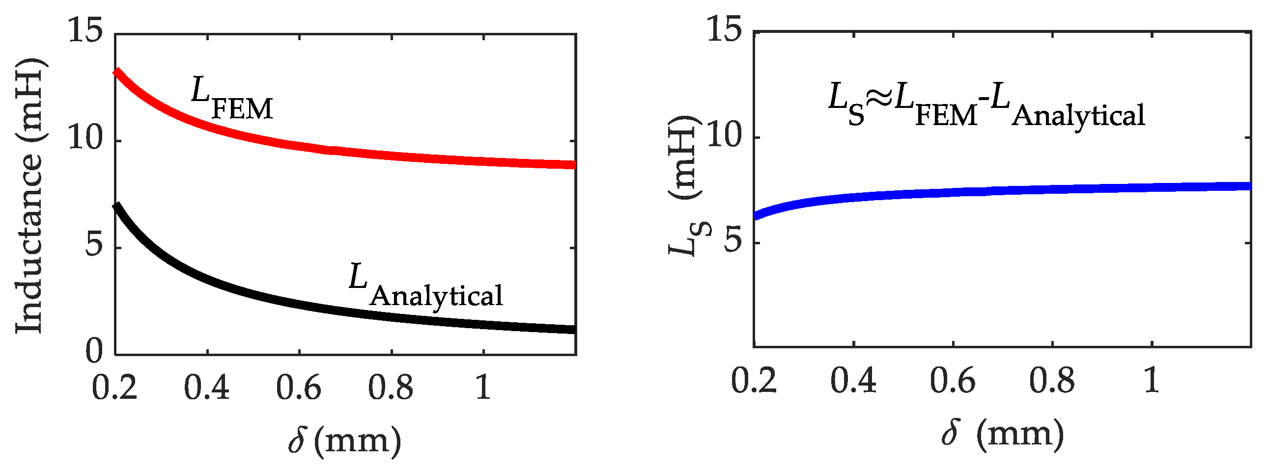
It is difficult to build an analytical model to accurately predict the leakage inductance of an inductive sensor. Therefore, we try to estimate the leakage inductance with the help of FEM. LAnalytical, LFEM are applied to express the inductance of an inductive sensor calculated by the traditional analytical model (Equation (3)) and by FEM, respectively, as shown in Figure 6. LFEM considers the leakage inductance LS while LAnalytical does not, hence, LS can be approximated by (LFEM-LAnalytical). Figure 6 shows the change trend of LAnalytical vs. δ curve and LFEM vs. δ curve is basically the same, which indicates that the leakage inductance is not sensitive to the change of air gap. In particular, when the air gap becomes larger, the leakage inductance approaches a constant that does not change with the air gap. In order to estimate the leakage inductance accurately in the design process, it is necessary to establish the functional relationship between the leakage inductance and the design parameters, such as the number of coil turns, the geometric size of core, etc. Parameter scanning using FEM analysis shows the relationship curves among LFEM, LS and N2, as shown in Figure 7a,b. In addition, we have found that LS is proportional to N2, thus, LS can be defined by,
where GS is a defined coefficient to calculate the leakage inductance, and N is the coil turns of the inductive sensor. GS is the slope of the fitting line of LS vs. N2 curve in Figure 7b, and GS = 7.4 × 10⁻⁶ here. GS of inductive sensors with different size can be obtained by the same method.
The calculation of leakage inductance with FEM is cumbersome and time-consuming, and the FEM model cannot be established before the preliminary design of geometric parameters is completed. Therefore, the FEM model can only be used for analysis, not for design. We expect that there is an expression that can capture the relationship between GS and the size of the sensor core. The cross section of sensor core can be chosen as a square with the side length of a, and a can be used to quickly and accurately estimate GS in the design process. Then, by Equation (7) and the known coil turns N, the leakage inductance can be quickly estimated. The relationship between GS and a is calculated, which has a good linearity, as shown in Figure 7c. An approximate expression of GS is obtained by linear fitting, that is,
Further analysis shows that the coefficient in front of a is close to the order of magnitude of the vacuum permeability μ0 = 4π × 10−7 H/m. Hence, we assume that GS is related to μ0, and GS can be expressed as,
where m, n are two parameters for inductive sensors. Combining Equations (8) and (9), yields m = 1.67 and n = 3.34. In addition, we can acquire an expression as follows,
Inserting Equation (10) into (7) yields,
Equation (3) is the traditional analytical model for calculating the inductance sensor, and the inductance obtained does not consider the leakage inductance. By adding the Equation (11) to Equation (3), we can obtain a modified analytical model of inductance vs. air gap characteristic:
where L* is the total inductance of inductive sensors, including the leakage inductance; a2 is the cross-sectional area (S = a2) of the air gap.
The effects of different permeability and conductivity of sensor core and different excitation frequency on the inductance of inductive sensors are analyzed by FEM. Figure 8 demonstrates the above modified model for estimating leakage inductance and total inductance is applicable to the inductive sensors with cores made of different permeable materials and with different excitation frequencies, as long as the cores have high permeability and low conductivity. For permeable materials with high conductivity, the laminated core can reduce the equivalent conductivity, so that it can also meet the requirements of the model.
According to the above analysis, combined with other basic electromagnetic theories, we summarize the applicable conditions of the above estimation model of leakage inductance of the inductive sensor:
- (1)
- Ensure the magnetic induction B works in the linear segment of the B-H curve of the core. If the induction corresponding to the maximum permeability is Bm, B < Bm must be satisfied;
- (2)
- It is suitable for the inductive sensor with the core of different permeable materials. However, the core materials with high permeability and low conductivity should be used whenever possible;
- (3)
- It is suitable for different excitation frequencies below 100 kHz;
- (4)
- The core must be the same as the structure proposed in this paper, and the core legs can also be cylindrical (correspondingly, a will represent the diameter of the cylindrical section of the core);
- (5)
- If the sizes of the core other than the dimension a have a significant change, the values of m, n in Equation (9) need to be corrected.
Using the above model can avoid tedious and time-consuming numerical calculations and help us to quickly calculate the leakage inductance. Based on the leakage inductance model, we can accurately predict the inductance vs. armature displacement characteristic of the inductive sensor, and better ensure the correct selection of the geometry parameters (such as the core size and the coil turns). Moreover, the sensitivity of the differential inductive sensor is closely related to the leakage inductance, which will be analyzed in Section 3.5. The calculation model of the leakage inductance can help designers to design the parameters of the sensor accurately according to the sensitivity requirements.
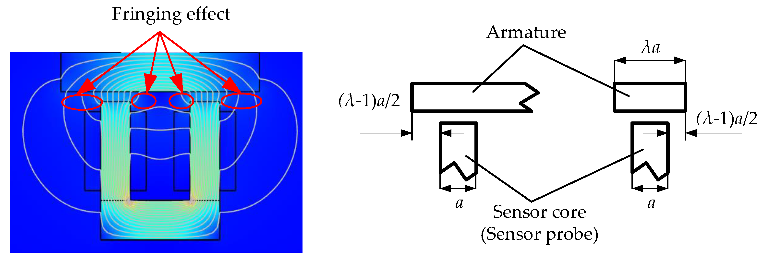
3.3. Fringing Effect Analysis and Armature Design Consideration
There is a fringing effect [10] at the edge of the sensor probe, as shown in Figure 9. Therefore, the geometric dimension of the armature needs to be considered. Assume that the side length of the sensor core is a, and the side length of the armature is λa. In the process of displacement sensing, the edge of the measured surface of the armature needs to exceed in the transverse direction out of the edge of the sensor probe. This can reduce the error caused by the transverse parasitic motion of the armature in practical application. The rule for selecting geometric dimensions of the armature is determined by considering the fringing effect. As shown in Figure 10, when λ approach to 2, the change trend of sensor inductance with λ slows down, thus we should select λ ≥ 2.
3.4. Measurement Circuit Factors
The measurement circuit of differential inductive sensors is simple, as shown in Figure 11. AC bridge is used as the front circuit. A pair of inductive sensor probes with identical geometrical and electrical parameters act as arms of the bridge. Their impedances are Z1 = j∙2πfL1 + r1, Z2 = j∙2πfL2 + r2, respectively. The input voltage of the bridge is Ũin, and the output voltage of the bridge is given by,
Ideally, when the armature is at zero position, the two sensor probes have the same inductance and resistance values. Hence, at zero, L1 = L2 = L0 + LS =
, r1 = r2 = r0. In a small range near zero position, L1 + L2 = 2,
r1 + r2 = 2r0, and the Q value of each probe is Q0 = 2πf/r0
when the armature at zero position, then Equation (13) can be converted to,
where ∆L = L1 − L2, ∆r = r1 − r2.
is the total zero inductance including the leakage inductance (LS). This equation contains two error terms with ∆r, which are in phase and orthogonal to Ũin, respectively. For the differential inductive sensor with large range, the error terms will be more complex. This is because the nonlinearity in the large range makes L1 + L2 and r1 + r2 not ideal constant values. These error terms will lead to large zero residual voltage, because it is difficult to ensure that the in-phase component and orthogonal component of the output voltage are zero at the same time when the armature is at the zero position. In addition, the existence of complex error terms will make it difficult to find a calibration curve whose mapping error meets the accuracy requirements. For example, for the calibration of the sensor with complex error terms, if the polynomial fitting curve is used as the calibration curve, higher order will be required, and even so, there may still be large mapping errors. Moreover, due to the existence of the error terms, the change of sensor resistance caused by temperature change will affect the stability of the sensor.
Therefore, the large range inductive sensor is required to have a Q value as high as possible, so that the error terms can be suppressed. As long as the Q value is large enough, Equation (13) can be simplified to,
According to the previous analysis, ∆L contains the displacement information of the armature, so the change of bridge output voltage Ũout reflects the armature displacement.
3.5. Sensitivity Analysis of Differential Inductive Sensors Considering Leakage Inductance
The resolution of the sensor is determined by the circuit noise and sensitivity. Therefore, correct prediction and design sensitivity are the key to ensure the measurement performance of the sensor. In a large range, the differential inductance sensor is nonlinear, and the sensitivity changes with displacement. The sensitivity near the zero position (∆δ = 0) is the smallest, so only the sensitivity near the zero position needs to be designed.
Near the zero position, the sensitivity of differential inductance relative to displacement is defined as KL, and the sensitivity of bridge output voltage (the measuring circuit shown in Figure 11 is used) relative to the measured displacement is defined as KU. Based on Equation (5), KL can be given by,
Convert the AC bridge voltage (Ũout and Ũin) in equation (15) into RMS value (Uout and Uin) for calculation, KU can be given by,
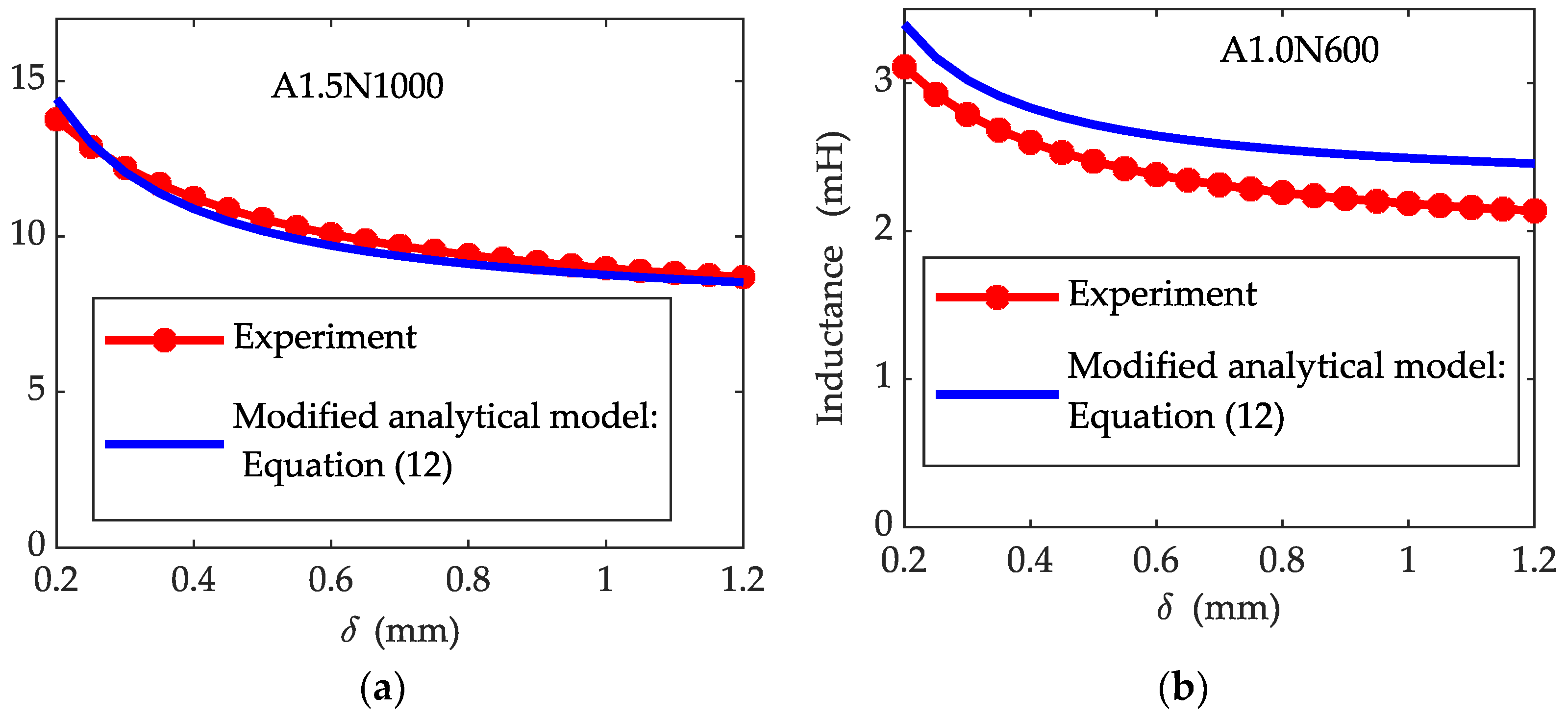
Equation (17) shows that the ratio of leakage inductance to zero working inductance (LS/L0) is an important factor affecting the sensitivity (KU) of differential inductance sensors. The smaller LS/L0, the higher KU. Therefore, the leakage inductance modeling in Section 3.2 plays an important role here, which is an important part of the differential inductive sensor design. According to the leakage inductance model (Equation (11)), the relationship between LS/L0 and the size of the sensor core is obtained, as shown in Figure 12. It shows that LS/L0 decreases with the increase of sensor core size. Therefore, if other conditions remain unchanged, the sensitivity of differential inductive sensors will increase with the increase of sensor core size.
If two of the designed prototypes (type: A1.5N1000; a = 1.5 mm) form a differential inductive sensor, and the excitation voltage is Uin=7 Vrms and the zero gap is δ0 = 0.7 mm. The theoretical sensitivity calculated based on Equation (17) and Figure 12 is,
And the sensitivity obtained from the experimental result is KU_Experiment = 0.71 mV/mm.
The deviation between KU_Theory and KU_Experiment may be due to the small Q value of the prototype sensor, coil winding process, and the installation error of sensor probes.
4. Q Value and Excitation Frequency Analysis
4.1. Basic Concept of Q Value
The quality factor of an inductive sensor is defined as Q, which is given by,
where f is the excitation frequency, L* = L+LS is the total inductance of inductive sensors, and r is the resistance of the sensor coil. Q value reflects the loss of the inductive sensor, and it is an important factor affecting the performance of inductive sensors.
For differential inductive sensors, increasing the Q value can reduce the error in principle, as mentioned in Section 3.4. In addition, increasing the excitation frequency can help improve the measurement bandwidth. Hence, we expect both the Q value and excitation frequency of the inductive sensor to be as large as possible. However, the Q value is influenced by the excitation frequency, which, in turn, is constrained by the Q value. They have a tremendous relationship with core loss, which will be discussed below.
4.2. Core Loss and Its Influence on Q Value of Inductive Sensors
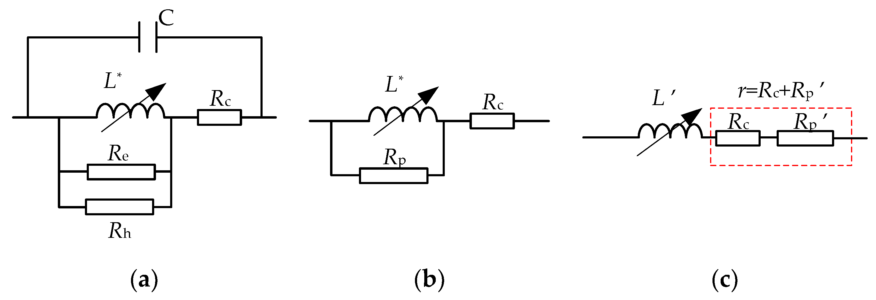
Core loss mainly includes hysteresis loss and eddy current loss [11], which can be embodied as the equivalent hysteresis loss resistance Rh and the equivalent eddy current loss Re resistance parallel to the coil inductance L*, respectively [12,13]. The equivalent circuit of an inductive coil is shown in Figure 13a, where Rc is the DC resistance of sensor coil and C is the parasitic capacitance. Through the impedance test, it is found that C is very small and can be ignored, as Figure 13b shows. Further, it can be equivalent to inductance and resistance in series, as shown in Figure 13c. The relevant derivation equation of the coil equivalent circuit parameters is as follows
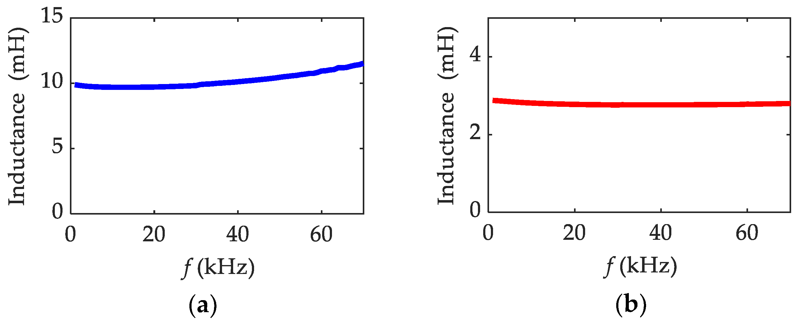
The increase of excitation frequency will lead to the increase of core loss, so as to reduce Rp, and then increase Rp’ and decrease L’. Generally, when the excitation frequency below 100 kHz, Rp is much greater than ωL*, so the change of L* is very small according to Equation (21), and that is L’≈L*, as shown in Figure 8c from FEM and Figure 22 from experimental results. Therefore, the main embodiment of the core loss is to increase the resistance r, which will cause the Q value of the inductive sensor to decrease according to Equation (18).
4.3. Selection Rule of Excitation Frequency
Figure 14a shows that appropriately increasing the excitation frequency f can increase the Q value. However, when the f increases to a certain value, the increase rate of core loss becomes faster, which makes the sensor resistance r increase quickly, resulting in the decrease of Q value. Therefore, in order to ensure a large Q value, it is necessary to select an appropriate excitation frequency. However, the excitation frequency corresponding to the maximum Q value in the Q vs. f curve may not be optimal, which will be analyzed in detail below.
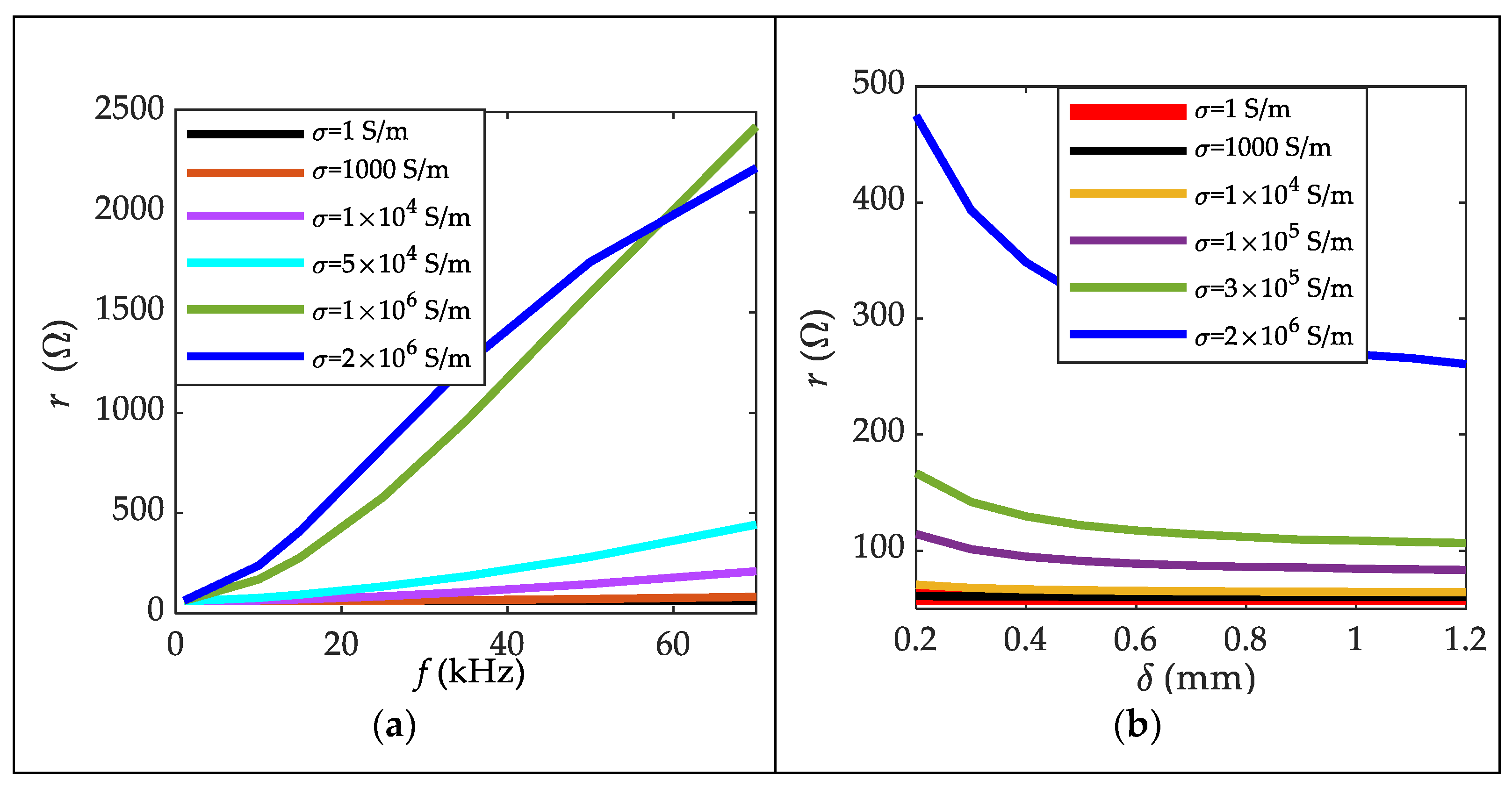
In fact, for the inductive sensor with large core loss, the resistance r of the inductive sensor changes greatly with the air gap, as shown in the FEM results (Figure 15) and experimental results (Figure 21). Ideally, the operating characteristics of inductive sensors are completely determined by L vs. δ relationship. If r vs. δ relationship is significant, it would greatly reduce the accuracy of the sensor. The significance of r vs. δ can be expressed as Q vs. δ. As can be seen from Equation (18), if the significance of r vs. δ is low, Q vs. δ and L vs. δ have the same change trend, and Q decreases with the increase of δ. However, if the significance of r vs. δ is very high, Q vs. δ and L vs. δ have the opposite trend, and Q increases with the increase of δ. For the latter, the change of r is very large with δ. In this case, even if Q value increases, it is difficult to suppress the adverse effect of r on the sensor with the change of δ.
Therefore, a selection rule of excitation frequency f is proposed, as shown in Figure 14. Meaning of each parameter in Figure 14a: Qm refers to the maximum value of the Q vs. f curve, and fm is the excitation frequency corresponding to Qm. Qr is the minimum Q value required by the sensor. If Qm ≥ Qr, there will be an excitation frequency corresponding to Qr, which is called fr (fr > fm). When the excitation frequency f increases to a certain value (defined as ft), the Q value begins to increase with the increase of air gap, and Qt is the defined value corresponding to ft. The frequency named fa is the minimum excitation frequency that meets the specific bandwidth requirement of the sensor. The selection of excitation frequency f can also be simply summarized into the following three steps:
- (1)
- Ensure the excitation frequency must not exceed the frequency at which the Q value begins to increase with the air gap (f ≤ ft);
- (2)
- Ensure the excitation frequency must be greater than the minimum excitation frequency required for the sensor bandwidth (f ≥ fa);
- (3)
- Determine whether the maximum Q value, corresponding to the frequency fa ≤ f ≤ ft, satisfies the required minimum Q value. If satisfied, the frequency corresponding to this maximum Q value is the optimum excitation frequency to be selected. If not, the sensor will need to be redesigned.
Two prototype sensor probes tested in this paper belong to Case1 of the design rule shown in Figure 14. However, their corresponding Qt values are both less than 10, which is far from meeting our requirements, as shown in Figure 23. Therefore, the current prototype sensors can be improved by increasing their Q value, so as to better ensure the performance of large range operation.
4.4. Analysis for Increasing Q Value and Excitation Frequency
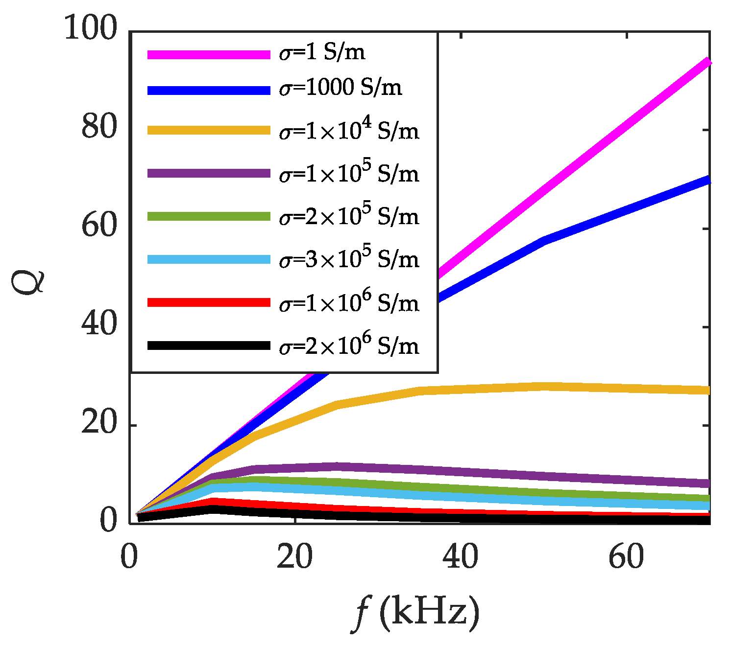
From the above analysis, we have known that coss loss is a culprit to limit the Q value and excitation frequency. Therefore, it is necessary to analyze the factors that determine the core loss, so as to help designers select appropriate methods to improve Q value and excitation frequency. The hysteresis loss of the iron core is directly proportional to the area of the hysteresis loop. Therefore, the coercivity of the core shall be as low as possible, and the induction B should work at a small value. The eddy current loss is mainly related to the conductivity of the core. The higher the conductivity, the greater the eddy current loss. Thus, the soft magnetic materials with as low conductivity as possible, such as ferrite, can be used to reduce the eddy current loss. However, the disadvantage of ferrite is its lower Curie temperature and its brittleness as a ceramic material. Soft magnetic alloys (such as Fe-Ni alloy) have perfect mechanical properties and high temperature stability, but the conductivity is too high (generally greater than 2 × 10⁶ S/m). For such materials, laminated core is generally used to suppress the eddy current loss.
From the point of view of suppressing the eddy current loss, the influences of material conductivity on resistance and Q value of the inductive sensor have been studied by FEM, as shown in Figure 15 and Figure 16. Here, we ignore the hysteresis loss and assume that there is only eddy current loss of inductive sensors due to the complexity of modeling and calculation of the hysteresis loss (Note: Because the hysteresis loss is ignored, the real value Q will be much lower than the FEM results. In addition, it is impossible for the Q value to increase indefinitely with increasing the excitation frequency). The FEM results show that with the increase of the core conductivity, the resistance of the inductive sensor increases, while the Q value decreases. Moreover, the excitation frequency corresponding to the maximum Q value of Q vs. f curve decreases as the core conductivity increases. The reduction of the allowable excitation frequency will hinder the improvement of the bandwidth of the sensor. We also find that when the core conductivity decreases to 1 × 10⁴ S/m, the eddy current loss resistance changes slowly with the excitation frequency. At the same time, as the excitation frequency increases, the Q value rises to a height and is no longer affected by the excitation frequency, and almost unchanged. In this case, the only factor limiting the actual Q value and the allowable excitation frequency is the hysteresis loss. Therefore, we come to a conclusion: If the conductivity of the selected core material is less than 1 × 10⁴ S/m, the eddy current losses are small enough that the core does not need to be laminated. Otherwise, the laminated core consisting of thin sheets must be used to suppress core loss. The selection rule of the thickness of sheets can refer to the calculation formula of the skin depth [13,14]:
where δe denotes the skin depth; μ and σ are the permeability and conductivity of the core, respectively; ω = 2πf. In theory, the thinner the sheet, the better the effect of suppressing eddy current loss. In addition, if the thickness of the sheet were much less than δe, the eddy current loss can be ignored. The thickness of the sheet is limited by the manufacturing process, which usually makes the core material with high conductivity unable to reach the sheet thickness required to suppress the eddy current loss. The sheet thickness required for soft magnetic materials with low conductivity is easier to obtain, so that the inductive sensor can achieve higher Q value and larger allowable excitation frequency. For example, amorphous alloys and nanocrystalline alloys exhibit more than 1-fold lower conductivity than that of Fe-Ni alloys and can better suppress the eddy current loss at the same sheet thickness. Ferrite cores with ultra-low conductivity may be ideal, do not require lamination and have little eddy current loss.
Without changing the core material, the Q value of inductive sensors can also be improved by optimizing the coil turns N and the core size. According to the FEM results shown in Figure 17a, increasing N can slightly increase the Q value. This is because the inductance increases with N. However, changing N cannot increase the allowable maximum excitation frequency of the inductive sensor, which proves that the allowable maximum excitation frequency is only determined by the core. Figure 17b shows that reducing the cross-section size of the core can also help improve the Q value and increase the allowable excitation frequency slightly, because the core loss power is directly proportional to the volume.
The methods of increasing Q value and excitation frequency f are briefly summarized, and the limitations to be considered in using these methods are indicated as follows:
- (1)
- The magnetically permeable material with lower conductivity can be selected as core. However, the precondition of low coercivity and high permeability is required. Moreover, if the ferrite with low permeability is selected, the temperature stability and fragility of the core need to be considered;
- (2)
- Reduce the thickness of sheets of the laminated core. We need to consider whether the corresponding manufacturing process can be achieved, and whether too thin sheets will reduce the permeability of the core;
- (3)
- Reduce the cross-sectional dimension of the core. It should be considered that the sensitivity of the sensor will be reduced and the winding of the coil may be more difficult.
- (4)
- Increase the number of coil turns. It is necessary to consider that the size of sensor probe will increase. In addition, the increase of coil turns is limited by the area of the core window; In addition, the increase of coil turns will also make it difficult to guarantee the precision of coil winding. It is noteworthy that increasing the coil turns can only increase the Q value, but the allowable excitation frequency can not be effectively improved.
5. Experimental Results
Two types prototype sensor probes (A1.5N1000 and A1.0N600) with different sizes based the structure shown in Figure 1 were used for experiments to support the previous analysis. The geometry and material specifications of them are shown in Table 2. The corresponding 3D model of the prototype sensor is shown in Figure 18a. The sensor probe size is within 6 mm × 6 mm × 3 mm, which ideally meets the miniaturization requirements.
An experimental platform is built as shown in Figure 18b. The target is driven by a spiral microprobe with a resolution of 1 μm. A capacitive sensor (Type: CSH05) supplied by MICRO-EPSILON is used as a reference standard, which has nanoscale resolution. A high-precision impedance analyzer is used to test the impedance of prototype sensors. In addition, a phase lock-in amplifier (Type: LF2LI) provided by Zurich Instruments is used to demodulate the analog signal from the differential inductive sensor.
Experiments are conducted mainly to obtain the impedance characteristics (inductance, resistance, Q) of prototype inductive sensor probes and the characteristic of differential inductive sensor. The obtained experimental results are directly used to support the analysis in this paper.
An impedance analyzer is used to measure the impedance-related quantity of the prototype sensor probes (A1.5N1000 and A1.0N600). Figure 19 and Figure 20 are mainly used to verify the correctness of the proposed leakage inductance model of the inductive sensor. Figure 21, Figure 22 and Figure 23 are mainly used in the analysis of Q value and excitation frequency.
The bridge circuit shown in Figure 11 and the lock-in amplifier (Type: MF2LI) are used to calibrate the differential inductive sensor composed of a pair of prototype sensor probes (Type: A1.5N1000). The input voltage of the bridge is 7 Vrms. In addition, according to the proposed excitation frequency selection method, the excitation frequency of 16 kHz is selected. Set the amplifier’s magnification of measurement circuit to 1. The experimental results are shown in Figure 24 and Table 3. RMS resolution was obtained by dividing the output peak to peak noise by the zero position sensitivity and dividing by a further 6.6. The sensor has a high resolution within a large range of ±0.5 mm, which proves the feasibility of large range operation of inductive sensors and validates the effectiveness of the analysis and design method proposal in this paper. According to the proposed analysis and design method, if the core material and other design parameters are improved, the Q value and excitation frequency will be further improved, which can greatly improve the large range operation performance of the inductive sensors.
6. Conclusions
A novel analysis and design method for the miniaturized inductive sensor with large measuring range and nanoscale resolution is proposed. Firstly, the leakage inductance model that can help designers design the parameters of large range differential inductive sensors more quickly and accurately is established. Secondly, a design rule of armature size is proposed by considering the fringing effect. Then, the complex error terms present in the transfer characteristic of differential inductive sensors are analyzed and the methods to suppress them are illustrated. Finally, A design rule including selecting the optimal excitation frequency is proposed to meet the requirements of high Q value and bandwidth and minimize the impact of core loss resistance on the performance of the sensor. Validated by experiments, the proposed analysis and design method can effectively guide the design of the inductive sensor with measuring range of ±0.5 mm. The fabricated inductive sensor prototypes realize the ideal miniaturization, and the overall size is limited to less than 6 mm × 6 mm × 3 mm. Combined with large measuring range, high resolution and miniaturization, such inductive sensors can be well suitable for the compact, large stroke nanopositioning system.
Author Contributions
Conceptualization, S.F., Q.H., N.C., D.F. and F.C.; data curation, Q.H.; formal analysis, Q.H.; investigation, Q.H., S.F. and R.T.; methodology, S.F., N.C., R.T., D.F. and F.C.; project administration, S.F.; supervision, S.F.; writing—original draft, Q.H.; writing—review and editing, S.F. All authors have read and agreed to the published version of the manuscript.
Funding
This research was funded by the National Natural Science Foundation of China, grant number No. 52075536.
Institutional Review Board Statement
Not applicable.
Informed Consent Statement
Not applicable.
Conflicts of Interest
The authors declare no conflict of interest.
References
- Polit, S.; Dong, J. Development of a high-Bandwidth XY nanopositioning stage for high-rate micro-/nanomanufacturing. IEEE ASME Trans. Mechatron. 2011, 16, 724–733. [Google Scholar] [CrossRef]
- Awtar, S.; Parmar, G. Design of a large range XY nanopositioning system. J. Mech. Robot. 2013, 5, 021008. [Google Scholar] [CrossRef] [Green Version]
- Fleming, A.J.; Leang, K.K. Design, Modeling and Control of Nanopositioning Systems; Springer International Publishing: Berlin, Germany, 2014. [Google Scholar]
- Fleming, A.J. A review of nanometer resolution position sensors: Operation and performance. Sens. Actuators A Phys. 2013, 190, 106–126. [Google Scholar] [CrossRef]
- Smith, S.T.; Seugling, R.M. Sensor and actuator considerations for precision, small machines. Precis. Eng. 2006, 30, 245–264. [Google Scholar] [CrossRef]
- Maresca, R.A. General method for designing low-temperature drift, high-bandwidth, variable-reluctance position sensors. Magn. IEEE Trans. 1986, 22, 118–123. [Google Scholar] [CrossRef]
- Philip, N.; George, B. Design and Analysis of a Dual-Slope Inductance-to-Digital Converter for Differential Reluctance Sensors. IEEE Trans. Instrum. Meas. 2014, 63, 1364–1371. [Google Scholar] [CrossRef]
- Velayudhan, C.; Bundell, J.H. Simple inductive displacement transducer. Rev. Sci. Instrum. 1984, 55, 1706–1713. [Google Scholar] [CrossRef]
- Wang, K.; Zhang, L.; Le, Y.; Zheng, S.; Han, B.; Jiang, Y. Optimized differential self-inductance displacement sensor for magnetic bearings: Design, analysis and experiment. IEEE Sens. J. 2017, 17, 4378–4387. [Google Scholar] [CrossRef]
- Cale, J.; Sudhoff, S.D.; Li-Quan, T. Accurately modeling EI core inductors using a high-fidelity magnetic equivalent circuit approach. IEEE Trans. Magn. 2006, 42, 40–46. [Google Scholar] [CrossRef]
- Aziz, M.; Indarto, A.; Hudaya, C. Study of material characteristics of core and winding to minimize losses on power transformer. IOP Conf. Ser. Earth Environ. Sci. 2021, 673, 012008. [Google Scholar] [CrossRef]
- Sato, T.; Sakaki, Y. Physical meaning of equivalent loss resistance of magnetic cores. IEEE Trans. Magn. 1990, 26, 2894–2897. [Google Scholar] [CrossRef]
- Zhu, J.G.; Hui, S.Y.R.; Ramsden, V.S. A generalized dynamic circuit model of magnetic cores for low-and high-frequency applications. I. Theoretical calculation of the equivalent core loss resistance. IEEE Trans. Power Electron. 1996, 11, 246–250. [Google Scholar] [CrossRef]
- Gawrylczyk, K.M.; Trela, K. Frequency response modeling of transformer windings utilizing the equivalent parameters of a laminated core. Energies 2019, 12, 2373. [Google Scholar] [CrossRef] [Green Version]
Figure 1.
Structure of an inductive sensor.

Figure 2.
Differential inductive sensors.

Figure 3.
∆L vs. x nonlinear relationship of differential inductive sensors operated in large range (∆L = L1 − L2).
Figure 3.
∆L vs. x nonlinear relationship of differential inductive sensors operated in large range (∆L = L1 − L2).

Figure 4.
The magnetic flux of inductive sensors given by FEM.

Figure 5.
The flux density B at different points.

Figure 6.
Inductance vs. air gap δ relationships obtained by FEM and analytical model, respectively.
Figure 6.
Inductance vs. air gap δ relationships obtained by FEM and analytical model, respectively.

Figure 7.
Relationships among LS, GS, N2 and a: (a) LFEM vs. N2; (b) LS vs. N2; (c) GS vs. a. Note: a is the side length of the core leg (whose cross section is square) of the inductive sensor.
Figure 7.
Relationships among LS, GS, N2 and a: (a) LFEM vs. N2; (b) LS vs. N2; (c) GS vs. a. Note: a is the side length of the core leg (whose cross section is square) of the inductive sensor.

Figure 8.
Effects of relative permeability, conductivity of sensor core and excitation frequency on the inductance of the inductive sensor, from FEM results: (a) Inductance vs. air gap relationships of the inductive sensor with the core of different relative permeability μr; (b) Inductance vs. air gap relationships of the inductive sensor with the core of different conductivity σ; (c) Inductance vs. excitation frequency of the inductive sensor with different air gap.

Figure 9.
Fringing effect and geometric dimension of armature.

Figure 10.
Relationship between sensor inductance and armature size.

Figure 11.
Simplified AC bridge measuring circuit of differential inducive sensors.

Figure 12.
Relationship between LS/L0 and a of the differential inductive sensors with the zero air gap of δ0 = 0.7 mm. Note: a is the side length of the sensor core leg.
Figure 12.
Relationship between LS/L0 and a of the differential inductive sensors with the zero air gap of δ0 = 0.7 mm. Note: a is the side length of the sensor core leg.

Figure 13.
Equivalent circuit of the inductive coil: (a) Equivalent circuit considering the copper loss resistance Rc, the eddy current loss resistance Re, the hysteresis loss resistance Rh; (b) Equivalent circuit ignoring the parasitic capacitance. (c) Equivalent series circuit.
Figure 13.
Equivalent circuit of the inductive coil: (a) Equivalent circuit considering the copper loss resistance Rc, the eddy current loss resistance Re, the hysteresis loss resistance Rh; (b) Equivalent circuit ignoring the parasitic capacitance. (c) Equivalent series circuit.

Figure 14.
A design rule considering Q value and excitation frequency f: (a) Q vs. f relationship; (b) Selection rule of excitation frequency f.
Figure 14.
A design rule considering Q value and excitation frequency f: (a) Q vs. f relationship; (b) Selection rule of excitation frequency f.

Figure 15.
Resistance, core conductivity and excitation frequency of inductive sensors: (a) The variation of resistance with excitation frequency of different core conductivity (δ = 0.2 mm); (b) The variation of resistance with air gap of different core conductivity (f = 15 kHz).
Figure 15.
Resistance, core conductivity and excitation frequency of inductive sensors: (a) The variation of resistance with excitation frequency of different core conductivity (δ = 0.2 mm); (b) The variation of resistance with air gap of different core conductivity (f = 15 kHz).

Figure 16.
The variation of Q wih excitation frequency of different core conductivity (δ = 0.2 mm).

Figure 17.
The variation of Q wih f of the inductive sensor of different coil turns and core sizes analyzed by FEM: (a) Q vs. f of different coil turns N (δ = 0.2 mm, a = 1.5 mm); (b) Q vs. f of different cross section side length (a) of the core (N = 1000, δ = 0.2 mm).
Figure 17.
The variation of Q wih f of the inductive sensor of different coil turns and core sizes analyzed by FEM: (a) Q vs. f of different coil turns N (δ = 0.2 mm, a = 1.5 mm); (b) Q vs. f of different cross section side length (a) of the core (N = 1000, δ = 0.2 mm).

Figure 18.
3D model of the inductive sensor and the experimental platform: (a) Corresponding 3D model of the prototype sensor; (b) Experimental platform.
Figure 18.
3D model of the inductive sensor and the experimental platform: (a) Corresponding 3D model of the prototype sensor; (b) Experimental platform.

Figure 19.
Inductance vs. air gap characteristics of prototype sensors with the excitation frequency of 16 kHz: (a) L-δ characteristic of A1.5N1000; (b) L-δ characteristic of A1.0N600.
Figure 19.
Inductance vs. air gap characteristics of prototype sensors with the excitation frequency of 16 kHz: (a) L-δ characteristic of A1.5N1000; (b) L-δ characteristic of A1.0N600.

Figure 20.
Comparion of L-δ charicteristics of prototype sensors with the excitation frequency of 16 kHz obtained by expriment and modified analytical model: (a) A1.5N1000; (b) A1.0N600.
Figure 20.
Comparion of L-δ charicteristics of prototype sensors with the excitation frequency of 16 kHz obtained by expriment and modified analytical model: (a) A1.5N1000; (b) A1.0N600.

Figure 21.
Influence of air gap δ and excitation frequency f on the resistance r of inductive sensors: (a) Relationship between r and δ of A1.5N1000 with the excitation frequency of 16 kHz; (b) Relationship between r and f of A1.5N1000 (δ = 0.7 mm); (c) Relationship between r and δ of A1.0N600 with the excitation frequency of 16 kHz; (d) Relationship between r and f of A1.0N600 (δ = 0.3 mm).


Figure 22.
Relationships between inductance and excitation frequency of prototype sensors tested by the high-precision impedance analyzer: (a) A1.5N1000 at δ = 0.7 mm; (b) A1.0N600 at δ = 0.3 mm.
Figure 22.
Relationships between inductance and excitation frequency of prototype sensors tested by the high-precision impedance analyzer: (a) A1.5N1000 at δ = 0.7 mm; (b) A1.0N600 at δ = 0.3 mm.

Figure 23.
The relationship curve between Q value and excitation frequency of two prototype sensor probes under different air gap: (a) Q vs. f of A1.5N1000; (b) Q vs. f of A1.0N600.
Figure 23.
The relationship curve between Q value and excitation frequency of two prototype sensor probes under different air gap: (a) Q vs. f of A1.5N1000; (b) Q vs. f of A1.0N600.

Figure 24.
Experimental results of the prototype differential inductive sensor (composed of A1.5N1000): (a) Output voltage vs. x characteristic; (b) Mapping error; (c) Peak to peak output noise.
Figure 24.
Experimental results of the prototype differential inductive sensor (composed of A1.5N1000): (a) Output voltage vs. x characteristic; (b) Mapping error; (c) Peak to peak output noise.


Table 1.
Typical commercial miniaturized nanometer displacement sensors.
| Sensor | Principle | Manufacturers | Size (mm) | Range (mm) | RMS Resolution (@100 Hz) |
|---|---|---|---|---|---|
| DIT-5200-15N | Eddy current | KAMAN | ∅4.78 × 28.6 | ±0.25 | 3.5 nm |
| CS02 | Capacitive | Micro-Epsilon | ∅6 × 12 | 0.2 | 0.15 nm (@2 Hz) |
| ES-U1 | Eddy current | Micro-Epsilon | ∅6 × 30 | 1 | 20 nm (@20 Hz) |
| KRS719(01) | LVDT | Micro-Epsilon | ∅10 × 16 | ±1 | 1.4 µm |
| D-510.021 | Capacitive | Physik Instrumente | ∅8 × 30 | 0.15 | 1.5 nm (@20 Hz) |
Table 2.
Geometry and material specifications of prototype sensors.
| Type | A1.5N1000 | A1.0N600 |
|---|---|---|
| a | 1.5 mm | 1.0 mm |
| Coil turns, N | 1000 | 600 |
| Wire diameter of coil, d | 0.05 mm | 0.05 mm |
| Core material | Laminated Ni-Fe alloy (50% Ni) | Ni-Fe alloy (50% Ni) |
| Coil material | Copper | Copper |
Table 3.
Performance of the prototype differential inductive sensor (composed of A1.5N1000).
| Range (mm) | Sensitivity at Zero Position (mV/μm) | RMS Resolution at Zero Position (nm) @100 Hz | RMS Resolution at Full Range (nm) @100 Hz | Maximum Mapping Error (%FSO) |
| ±0.5 | 0.71 | 2.2 | 13 | 0.1 |
Publisher’s Note: MDPI stays neutral with regard to jurisdictional claims in published maps and institutional affiliations. |
© 2021 by the authors. Licensee MDPI, Basel, Switzerland. This article is an open access article distributed under the terms and conditions of the Creative Commons Attribution (CC BY) license (https://creativecommons.org/licenses/by/4.0/).
Share and Cite
MDPI and ACS Style
He, Q.; Fan, S.; Chen, N.; Tan, R.; Chen, F.; Fan, D. Analysis of Inductive Displacement Sensors with Large Range and Nanoscale Resolution. Appl. Sci. 2021, 11, 10134. https://doi.org/10.3390/app112110134
AMA Style
He Q, Fan S, Chen N, Tan R, Chen F, Fan D. Analysis of Inductive Displacement Sensors with Large Range and Nanoscale Resolution. Applied Sciences. 2021; 11(21):10134. https://doi.org/10.3390/app112110134
Chicago/Turabian StyleHe, Qiang, Shixun Fan, Ning Chen, Ruoyu Tan, Fan Chen, and Dapeng Fan. 2021. "Analysis of Inductive Displacement Sensors with Large Range and Nanoscale Resolution" Applied Sciences 11, no. 21: 10134. https://doi.org/10.3390/app112110134
Note that from the first issue of 2016, this journal uses article numbers instead of page numbers. See further details here.