The Influence of Quantum Confinement on Third-Order Nonlinearities in Porous Silicon Thin Films

School of Physics and Astronomy, University of Birmingham, Birmingham B15 2TT, UK
*
Author to whom correspondence should be addressed.
Appl. Sci. 2018, 8(10), 1810; https://doi.org/10.3390/app8101810
Submission received: 14 September 2018
/
Revised: 26 September 2018
/
Accepted: 28 September 2018
/
Published: 3 October 2018
(This article belongs to the Special Issue Nanoporous Materials and Their Applications)
Abstract
:We present an experimental investigation into the third-order nonlinearity of conventional crystalline (c-Si) and porous (p-Si) silicon with Z-scan technique at 800-nm and 2.4-m wavelengths. The Gaussian decomposition method is applied to extract the nonlinear refractive index, , and the two-photon absorption (TPA) coefficient, , from the experimental results. The nonlinear refractive index obtained for c-Si is cm/GW and for p-Si is cm/GW. The TPA coefficient was found to be cm/GW and cm/GW for c-Si and p-Si, respectively. We show an enhancement of the nonlinear refraction and a suppression of TPA in p-Si in comparison to c-Si, and the enhancement gets stronger as the wavelength increases.
1. Introduction
Porous silicon (p-Si) has attracted great interest in recent years due to its unique opto-electronic properties. The nanoscale sponge-like structure of p-Si, whereas porosity significantly enlarges its surface-to-volume ratio, exhibits the quantum confinement effect [1], resulting in faster carrier recombination [2], accompanied, at certain conditions, by photo-luminescence [3] and optical nonlinearities [4]. These effects are usually greatly enhanced in comparison to the conventional crystalline silicon (c-Si). These new capabilities extend the implementation of the traditional silicon material in photonics and optoelectronics to a wider range of potential applications of all-optical switching [5,6], optical sensing [7,8], energy conservation [9] and photonics devices [10]. However, possible applications encountering the enhanced nonlinearities of p-Si can be either an issue or advantage. Unwanted non-linear effects may result in sample damage through the undesirable self-focusing and two-photon absorption effects. However, the same effects may also bring advantages such as the use of p-Si as a material for 3D-laser micro-structuring [11] and an all-optical switching system [12]. Yet, the information on p-Si nonlinearity remains scarce, and our work attempts to form a clearer understanding of the topic through investigating the self-focusing and two-photon absorption (TPA) processes. For the investigation, we employed the Z-scan technique using 800-nm and 2.4-m femtosecond laser beams.
The Z-scan is the main method used in this work. It was first proposed by Sheikh-Bahae et al. [13] in the 1990s for identifying the third-order nonlinearities of materials by translating a test sample through the focus of a Gaussian beam and recording the transmittance at each sample position. This method is highly sensitive and gives distinguishable features for the measurements of the near (closed aperture) and far (open aperture) field transmittance, corresponding to the nonlinear refraction and TPA processes, respectively. For nonlinearly refractive materials, a higher intensity in the centre of the Gaussian beam, in comparison to its surroundings, results in a variation of the refractive index along the beam cross-section. Therefore, samples behave as a focusing or defocusing lens depending on the sign of the nonlinear refractive index, . This effect can be observed by recording only the centre intensity of the transmitted light, which is normally accomplished by placing an aperture before a detector. In contrast, the total transmitted intensity (without the aperture) carries the information about nonlinear absorption, as it records a change of the total beam intensity, which is commonly governed by the TPA.
The main purpose of this work is to compare nonlinear properties of p-Si to c-Si and to examine possible effects of the morphology and confinement. We employed the Z-scan method for both p-Si and c-Si using 800-nm incident light, which has photon energy greater than the band-gap of both materials. The majority of researchers focus on this energy regime because the nonlinear response benefits from strong single-photon resonance enhancement [14]. However, to have a better understanding of the nonlinearities arising from the anharmonic motion of bound electrons, we further extended the experiments to 2.4 m, where the incident light energy is below the band-gap. We measured the normalised transmittance, , with a closed and open aperture for p-Si and c-Si free-standing thin films with a 15- and 9-m thickness, respectively. Here, is the measured transmittance at a sample position z, relative to the location of the beam focus and is the linear transmittance. The acquired experimental data were used to retrieve the nonlinear refractive index, , and TPA coefficient, . For the data analysis, we applied the Gaussian decomposition method [15]. The results suggest a suppression of the TPA, but an enhancement of the nonlinear refraction in p-Si. In addition, the closed aperture Z-scan measurements of p-Si showed an opposite sign of in comparison with c-Si.
2. Results
For the sample being translated through the focus of a beam with a Gaussian profile and considering only the third order nonlinearity, the total time-integrated transmission, , for the open aperture can be expressed as [16,17,18]:
where is the on-axis peak intensity and is the effective optical length of the sample with thickness d and linear absorption coefficient . z is the sample position relative to the beam focal point, and is the confocal parameter of the beam with waist and wavelength .
For the closed aperture, the transmittance is given by:
here, is the time-averaged phase change induced by the nonlinear refraction, which can be approximated as:
where S is the transmissivity of the aperture.
The Gaussian decomposition method requires the proper determination of the effective optical length, , which can be deduced from the linear optical constants of the c-Si and p-Si samples. For the c-Si samples, the linear absorption coefficient can be estimated by , where k is the imaginary part of linear refractive index. At an 800-nm wavelength, , as it was estimated by the spectroscopic ellipsometry method by Aspnes et al. [19], corresponding to cm. However, the refractive index and absorption coefficient values for p-Si are less known since these values depend on the porosity, silicon skeleton dimensionality and surface adsorbates [20]. It has been shown previously that the Maxwell–Garnett mixing rules can be applied in order to calculate the linear complex permittivity of p-Si at 800 nm [21,22]:
where and are the permittivity of c-Si and air pores (), respectively. f is the volume fraction of air pores, which was estimated to be 68% for the samples used in this work. Thus, we obtain that and cm. It is worth mentioning that the Maxwell–Garnett mixing rules are valid for these samples since the wavelength is about two orders of magnitude greater than the dimensions of the p-Si components.
As for the 2.4-m wavelength, there were no explicitly known values for the imaginary part of the refractive index of intrinsic c-Si. This was due to the insignificant absorption for the incident photon energy much smaller than the band-gap. However, the silicon skeleton of p-Si that was used in this work was boron-doped, which provided about 3 cm free carriers [23]. Hence, the free carrier absorption needed to be considered, which further led to an increase of the k value. The influence of free carriers introduced by boron dopants on the c-Si dielectric function can be estimated using the Drude model:
where N is the carrier concentration induced by dopants, e denotes the electron charge, is the effective hole mass and is the vacuum permittivity. The carrier-carrier scattering rate was chosen to be , which is a typical value for doped silicon [24]. Further use of the Maxwell–Garnett model for the p-Si provided the value of the dielectric function of . The corresponding absorption coefficient, , was cm at 2.4 m. We note that the dopant-induced free carrier absorption was about two orders of magnitude lower than the intrinsic absorption of silicon at 800 nm. Therefore, it could be safely discarded in the calculations for an 800-nm wavelength.
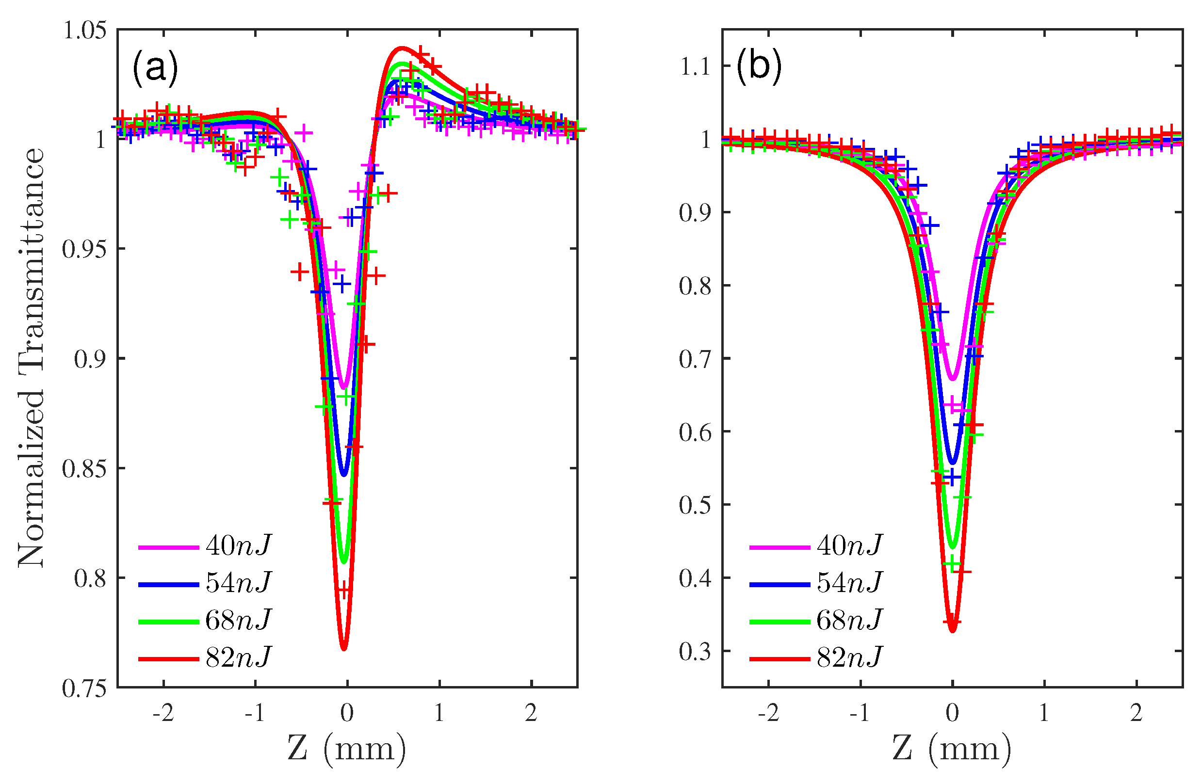
Figure 1a,b shows the measurements taken with the closed and open aperture, respectively, of Z-scan transmittance of the 9 m-thick c-Si thin film, using incident fluences of 40, 54, 68 and 82 nJ. The experimental results were fitted with Equations (1) and (2) to extract the TPA coefficient, , and nonlinear refractive index, . The fitting results suggest that cm/GW, while cm/GW, which are comparable to those previously published elsewhere [16,17]. The main reason for the observed uncertainties was due to the experimental error of the beam fluence determination. The fluence of the incident light did not exceed the nano-Joule range, and it was difficult to measure its exact value. The error involved in the measurements of the fluence was up to 30%. However, this should not lead to a severe numerical error and deviation from the acceptable standards for these types of experiments.
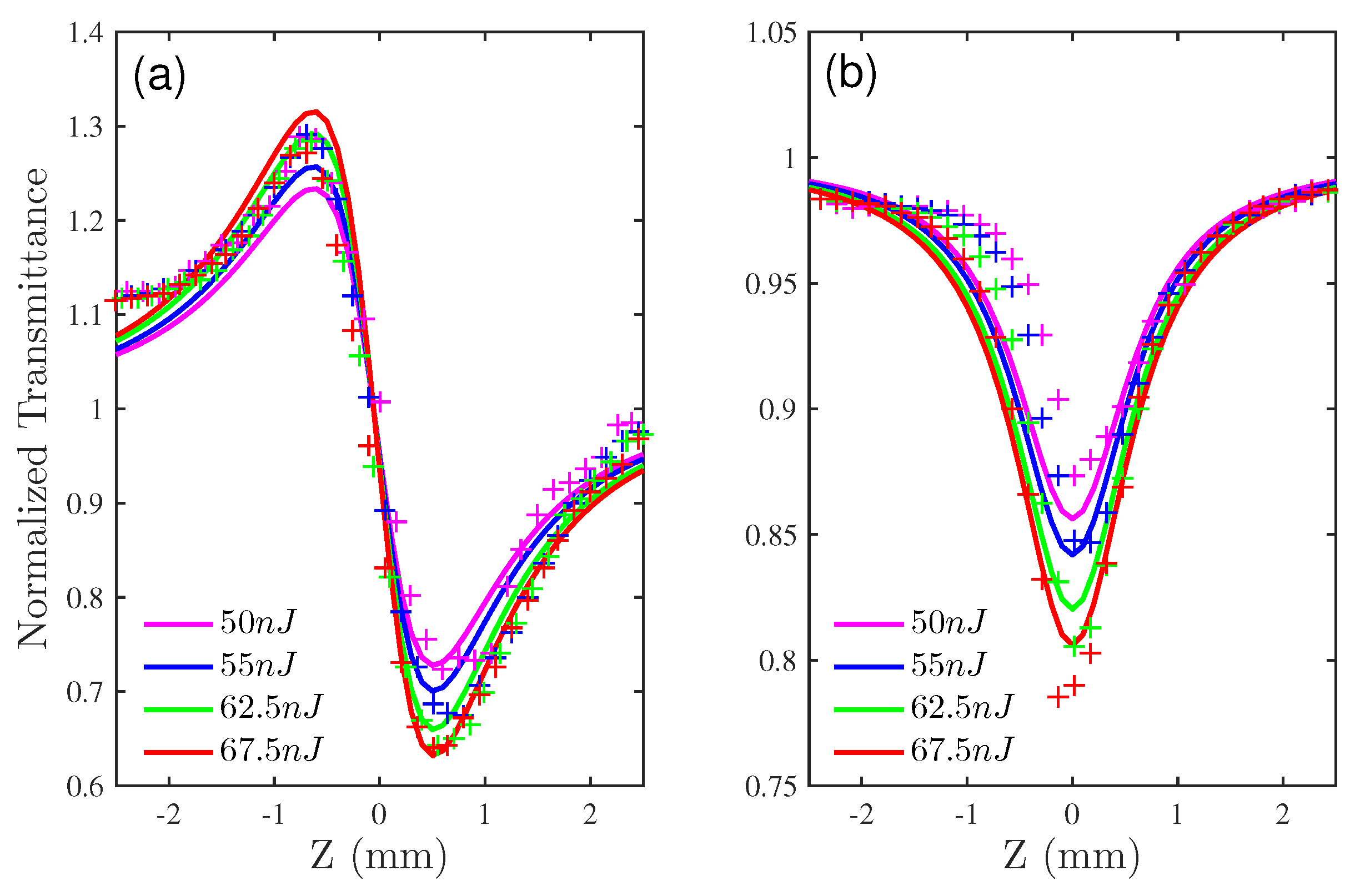
The experimental procedure was repeated to measure the non-linear response of a 15 m-thick free-standing p-Si thin film, and the results are shown in Figure 2. We note, the incident fluence covered a slightly different range than that used for the c-Si’s measurements. This was due to the difficulties in controlling the fluence level in such a low pulse energy range. The analysis revealed the TPA coefficient cm/GW and nonlinear refractive index cm/GW. In comparison with that of c-Si, the TPA appeared to be slightly suppressed. However, the nonlinear refraction was greatly enhanced. Remarkably, the sign of was reversed to the negative in comparison to the positive value of c-Si. These findings agree with Lettieri’s work [25] on p-Si, despite the fact that we used samples with different doping and porosity.
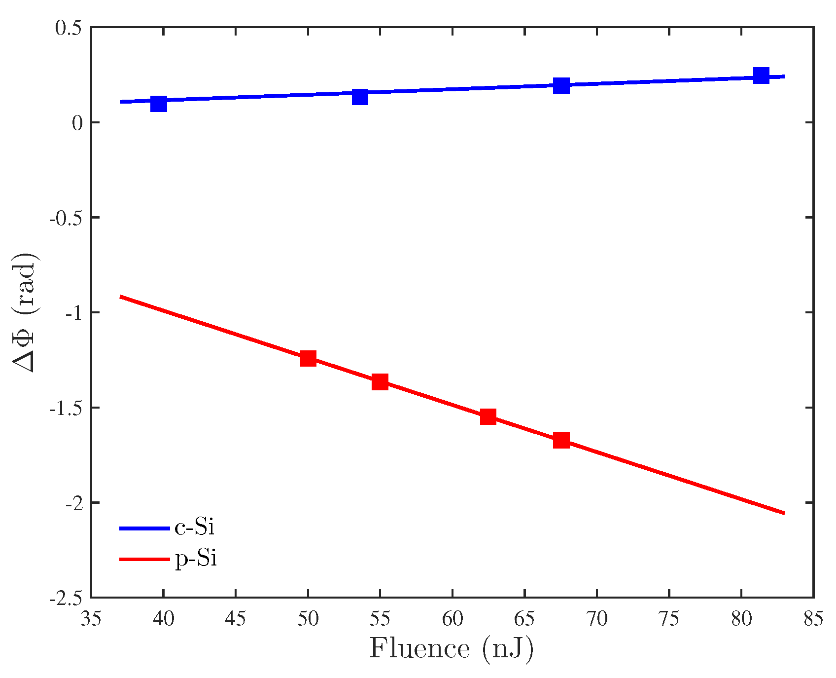
To further compare the nonlinear refraction process between c-Si and p-Si, the nonlinear phase shift for different incident fluences is plotted in Figure 3. The squares represent the experimental values , and the solid lines are calculated from Equation (3) with the values of obtained from the Z-scan measurements. It can be seen that the phase shift for p-Si was at least four-times higher and changed faster as a function of the fluence than that of the c-Si, which further confirmed the enhancement of the nonlinear refraction.
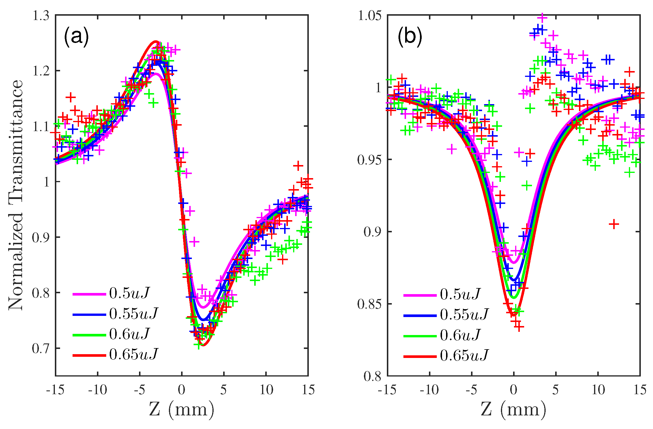
To further extend our knowledge about p-Si nonlinearity, we performed the experiments in the Short Wavelength Infrared (SWIR) where the photon energy is lower than the band-gap. Figure 4 shows the Z-scan results of p-Si at the wavelength of 2.4 m. Because of the detectors’ poor sensitivity at this wavelength range, the fluence was increased by an order of magnitude. The use of the longer wavelength required an increase in the scanning range from 5 mm to 30 mm to capture the stretched Z-scan features for both the closed and the open aperture cases. Due to the low level of the TPA at 2.4 m, the open aperture experiments, as shown in Figure 4b, encountered a high noise level and problems preventing achieving the optimal alignment. The combination of these factors led to a distortion of the symmetrical shape about zero and a higher absolute error in the determination of the TPA coefficient. By fitting the experimental results, we obtained the nonlinear coefficients cm/GW and cm/GW, indicating that the nonlinear refraction was even stronger for the longer wavelength range and that nonlinear absorption process was further restrained.
3. Discussion
The porous silicon used in this work consists of quasi-one-dimensional wires with a mean diameter of 10 nm. Therefore, the motion of the charged carriers is moderately confined. As a result of the confinement effect, the optical matrix element, defining the third order-nonlinear susceptibility (), increases. S. Lettieri et al. [25] proposed a computational model to calculate as a function of quantum wire radius. It was suggested that for a quantum wire with a 2–3.5-nm radius, the real part of is about four orders of magnitude greater than in the bulk. From our experimental results, we obtained m/V for p-Si, which is an order of magnitude greater than m/V for c-Si. The difference of our result as compared to Lettieri’s work might be the weaker confinement in our samples.
Moreover, in addition to the confinement, the optical Stark effect plays an important role in low-dimensional systems and can cause the sign reversal of (proportional to ) in p-Si. To demonstrate this effect, D. Cotter et al. employed the sum-over-states method for the calculation of of a sphere in a quantum confinement regime as a function of the sphere radius [14]. The results demonstrated that is always negative with positive values of . This behaviour is different from the bulk materials, which exhibit negative values only for photon frequencies very close to the absorption edge.
Our experimental results also show a suppression of the TPA process for an 800-nm photon wavelength and smaller in p-Si with respect to c-Si. However, it should be noted that the TPA coefficient we evaluated in this work is an effective value of p-Si. Due to the dilution of silicon with air, the effective is smaller than that of the silicon constituent, despite possible enhancement by the quantum confinement effect.
In summary, p-Si is a nonlinear material where the nonlinear refraction is greatly enhanced, but the nonlinear absorption is slightly suppressed with respect to its bulk counterpart. Such combinations of the coefficients make p-Si a suitable material for all-optical switching. The requirement for all optical switching is , where is the wavelength and is a switching parameter [26], the value of which depends on a particular switching scheme. For example, for a nonlinear coupled waveguide, . Our results suggest that for 800-nm p-Si and c-Si, and , respectively. However, at 2.4 m, p-Si gives a promising value for all-optical switching application since . In comparison to other semiconductor composites that have been proposed for all-optical switching (for example Al-Ga-As [27], Ge-As-Se and Ge-As-S-Se demonstrated [28]), p-Si has the advantage of the established fabrication technology, relatively low cost and less contamination to the environment.
4. Materials and Methods
4.1. Femtosecond Laser System
The experiments in this work were carried out using a Coherent femtosecond laser system. The seed laser was generated from a mode-locked oscillator and further amplified in a Q-switched amplification cavity. The output laser beam has a spatial Gaussian distribution, and the central wavelength was around 800 nm with a 100-nm spectral width. The pulse duration was about 60 fs with a 1-kHz repetition rate. More information on the laser system can be found elsewhere [6,22,29]. In addition, an optical parametric amplifier (OPerA-Solo) was used for the generation of a 2.4-m short infrared laser. The samples were placed on a motorised linear stage (VT-80) and translated through the focus of the Gaussian beam with a step size of 0.15 mm. The beam was focused to a minimum beam waist of 16 m by an N-BK7 Plano-convex lens with a 60-mm focal length. The pulse fluence was controlled by a half-wave plate combined with a linear polariser, which sets the polarisation to the in-plane direction (p-polarised). All experiments were conducted at the normal incidence. We note that in general, p-Si can be classified as a uniaxial birefringent material with the optical axis aligned along the pores’ direction [30,31,32]. However, at the normal incidence, there is no electric field component parallel to that axis, and the material can be treated as ordinary. A 45%/55% beam splitter was placed behind the sample, which splits the transmitted signal to two identical detectors, one with a 500-m aperture () in front and one without for the closed and open aperture measurements, respectively. Silicon detectors with a mm detection area were used for the 800-nm Z-scan and PbS detectors for the 2.4-m Z-scan.
4.2. Sample Preparation
Electro-chemical anodization was used for the preparation of p-Si samples. A boron-doped Si (100) wafer (resistivity: 5 to 15 mcm) was immersed in a mixture of methanol and 40% hydrofluoric acid electrolyte (mixing ratio 1:1). A current density of 30 mA/cm was then applied for the anodization process. The p-Si layer was separated from the underlying substrate by applying a short pulsed current with the current density of 120 mA/cm. The membrane was then rinsed in methanol and dried in air. A porosity of 68% was measured using gravimetric analysis, and the thickness of 15 m was estimated from the images of the cross-section obtained by a scanning electron microscope. The structure of the obtained samples can be described as sponge-like silicon material consisting of interwoven wires with a mean diameter of about 10 nm. More details about the sample characterisation can be found in [23,33].
5. Conclusions
In conclusion, we reported an enhancement on nonlinear refraction and suppression on TPA of p-Si in comparison with c-Si at 800 nm. The nonlinear refractive indices that we obtained for c-Si and p-Si are cm/GW and cm/GW, respectively. The TPA coefficient was determined to be cm/GW for c-Si and cm/GW for p-Si. In addition, a further increase of and a decrease of were found with an incident wavelength of 2.4 m. We believe that the quantum confinement in p-Si is the main reason for the above findings.
Author Contributions
Conceptualization, Andrey Kaplan; Data curation, Rihan Wu; Formal analysis, Rihan Wu; Methodology, Leigh Canham; Software, Jack Collins; Supervision, Andrey Kaplan; Writing—original draft, Rihan Wu; Writing—review & editing, Jack Collins, Leigh Canham and Andrey Kaplan.
Funding
This research received no external funding.
Acknowledgments
We would like to thank Emmalene Wilson for her contributions on developing the Z-scan method and Dimitri Chekulaev for his help with the laser system.
Conflicts of Interest
The authors declare no conflict of interest.
References
- Lehmann, V.; Gosele, U. Porous silicon formation: A quantum wire effect. Appl. Phys. Lett. 1991, 58, 856–858. [Google Scholar] [CrossRef]
- Zakar, A.; Park, S.J.; Zerova, V.; Kaplan, A.; Canham, L.T.; Lewis, K.L.; Burgess, C.D. MWIR optical modulation using structured silicon membranes. Int. Soc. Opt. Photonics 2016, 9992, 999203. [Google Scholar] [CrossRef]
- Cullis, A.G.; Canham, L.T.; Calcott, P.D.J. The structural and luminescence properties of porous silicon. J. Appl. Phys. 1997, 82.3, 909–965. [Google Scholar] [CrossRef]
- Klimov, V.; McBranch, D.; Karavanskii, V. Strong optical nonlinearities in porous silicon: Femtosecond nonlinear transmission study. Phys. Rev. B 1995, 52, R16989. [Google Scholar] [CrossRef]
- Henari, F.Z.; Morgenstern, K.; Blau, W.J.; Karavanskii, V.A.; Dneprovskii, V.S. Third order optical nonlinearity and all-optical switching in porous silicon. Appl. Phys. Lett. 1995, 67, 323–325. [Google Scholar] [CrossRef]
- Park, S.J.; Zakar, A.; Zerova, V.L.; Chekulaev, D.; Canham, L.T.; Kaplan, A. All-optical modulation in Mid-Wavelength Infrared using porous Si membranes. Sci. Rep. 2016, 6, 30211. [Google Scholar] [CrossRef] [PubMed] [Green Version]
- Lin, V.S.Y.; Motesharei, K.; Dancil, K.P.S.; Sailor, M.J.; Ghadiri, M.R. A porous silicon-based optical interferometric biosensor. Science 1997, 278, 840–843. [Google Scholar] [CrossRef] [PubMed]
- Dancil, K.P.S.; Greiner, D.P.; Sailor, M.J. A porous silicon optical biosensor: Detection of reversible binding of IgG to a protein A-modified surface. J. Am. Chem. Soc. 1999, 121, 7925–7930. [Google Scholar] [CrossRef]
- Menna, P.; Di Francia, G.; La Ferrara, V. Porous silicon in solar cells: A review and a description of its application as an AR coating. Sol. Energy Mater. Sol. Cells 1995, 37, 13–24. [Google Scholar] [CrossRef]
- Li, Y.Y.; Cunin, F.; Link, J.R.; Gao, T.; Betts, R.E.; Reiver, S.H.; Chin, V.; Bhatia, S.N.; Sailor, M.J. Polymer replicas of photonic porous silicon for sensing and drug delivery applications. Science 2003, 299, 2045–2047. [Google Scholar] [CrossRef] [PubMed]
- Qiu, J. Femtosecond laser-induced microstructures in glasses and applications in micro-optics. Chem. Rec. 2004, 4, 50–58. [Google Scholar] [CrossRef] [PubMed]
- Ashkenasi, D.; Varel, H.; Rosenfeld, A.; Henz, S.; Herrmann, J.; Cambell, E.E.B. Application of self-focusing of ps laser pulses for three-dimensional microstructuring of transparent materials. Appl. Phys. Lett. 1998, 72, 1442–1444. [Google Scholar] [CrossRef]
- Sheik-Bahae, M.; Said, A.A.; Wei, T.H.; Hagan, D.J.; Van Stryland, E.W. Sensitive measurement of optical nonlinearities using a single beam. IEEE J. Quantum Electron. 1990, 26, 760–769. [Google Scholar] [CrossRef]
- Cotter, D.; Burt, M.G.; Manning, R.J. Below-band-gap third-order optical nonlinearity of nanometer-size semiconductor crystallites. Phys. Rev. Lett. 1992, 68, 1200. [Google Scholar] [CrossRef] [PubMed]
- Weaire, D.; Wherrett, B.S.; Miller, D.A.B.; Smith, S.D. Effect of low-power nonlinear refraction on laser-beam propagation in InSb. Opt. Lett. 1979, 4, 331–333. [Google Scholar] [CrossRef] [PubMed]
- Dinu, M.; Quochi, F.; Garcia, H. Third-order nonlinearities in silicon at telecom wavelengths. Appl. Phys. Lett. 2003, 82, 2954–2956. [Google Scholar] [CrossRef]
- Bristow, A.D.; Rotenberg, N.; Van Driel, H.M. TPA and Kerr coefficients of silicon for 850–2200 nm. Appl. Phys. Lett. 2007, 90, 191104. [Google Scholar] [CrossRef]
- Gu, B.; Chen, J.; Fan, Y.X.; Ding, J.; Wang, H.T. Theory of Gaussian beam Z scan with simultaneous third-and fifth-order nonlinear refraction based on a Gaussian decomposition method. JOSA B 2005, 22, 2651–2659. [Google Scholar] [CrossRef]
- Aspnes, D.E.; Studna, A.A. Dielectric functions and optical parameters of Si, Ge, GaP, GaAs, GaSb, InP, InAs, and InSb from 1.5 to 6.0 ev. Phys. Rev. B 1983, 27, 985. [Google Scholar] [CrossRef]
- Canham, L. (Ed.) Handbook on Porous Silicon; Springer: Basel, Switzerland, 2014; ISBN 978-3-319-05744-6. [Google Scholar]
- Sihvola, A.H. Electromagnetic Mixing Formulas and Applications, Clarricoats, P.J.B., Jull, E.V., Eds.; The Institute of ElectricalEngineers: London, UK, 1999; ISBN 9780852967720. [Google Scholar]
- Chekulaev, D.; Garber, V.; Kaplan, A. Free carrier plasma optical response and dynamics in strongly pumped silicon nanopillars. J. Appl. Phys. 2013, 113, 143101. [Google Scholar] [CrossRef]
- Zakar, A.; Wu, R.; Chekulaev, D.; Zerova, V.; He, W.; Canham, L.; Kaplan, A. Carrier dynamics and surface vibration-assisted Auger recombination in porous silicon. Phys. Rev. B 2018, 97. [Google Scholar] [CrossRef]
- Qiu, B.; Tian, Z.; Vallabhaneni, A.; Liao, B.; Mendoza, J.M.; Restrepo, O.D.; Ruan, X.; Chen, G. First-principles simulation of electron mean-free-path spectra and thermoelectric properties in silicon. Europhys. Lett. 2015, 109, 57006. [Google Scholar] [CrossRef] [Green Version]
- Lettieri, S.; Fiore, O.; Maddalena, P.; Ninno, D.; Di Francia, G.; La Ferrara, V. Nonlinear optical refraction of free-standing porous silicon layers. Opt. Commun. 1999, 168, 383–391. [Google Scholar] [CrossRef]
- Sheik-Bahae, M.; Hutchings, D.C.; Hagan, D.J.; Van Stryland, E.W. Dispersion of bound electron nonlinear refraction in solids. IEEE J. Quantum Electron. 1991, 27, 1296–1309. [Google Scholar] [CrossRef]
- Siviloglou, G.A.; Suntsov, S.; El-Ganainy, R.; Iwanow, R.; Stegeman, G.I.; Christodoulides, D.N.; Pozzi, F. Enhanced third-order nonlinear effects in optical AlGaAs nanowires. Opt. Express 2006, 14, 9377–9384. [Google Scholar] [CrossRef] [PubMed]
- Harbold, J.M.; Ilday, F.O.; Wise, F.W.; Aitken, B.G. Highly nonlinear Ge-As-Se and Ge-As-S-Se glasses for all-optical switching. IEEE Photonics Technol. Lett. 2002, 14, 822–824. [Google Scholar] [CrossRef]
- Roger, T.W.; He, W.; Yurkevich, I.V.; Kaplan, A. Enhanced carrier-carrier interaction in optically pumped hydrogenated nanocrystalline silicon. Appl. Phys. Lett. 2012, 101, 141904. [Google Scholar] [CrossRef]
- Cazzanelli, M.; Kovalev, D.; Dal Negro, L.; Gaburro, Z.; Pavesi, L. Polarized optical gain and polarization-narrowing of heavily oxidized porous silicon. Phys. Rev. Lett. 2004, 93, 207402. [Google Scholar] [CrossRef] [PubMed]
- Kunzner, N.; Diener, J.; Gross, E.; Kovalev, D.; Timoshenko, V.Y.; Fujii, M. Form birefringence of anisotropically nanostructured silicon. Phys. Rev. B 2005, 71, 195304. [Google Scholar] [CrossRef]
- Golovan, L.A.; Timoshenko, V.Y.; Fedotov, A.B.; Kuznetsova, L.P.; Sidorov-Biryukov, D.A.; Kashkarov, P.K.; Diener, J. Phase matching of second-harmonic generation in birefringent porous silicon. Appl. Phys. B 2001, 73, 31–34. [Google Scholar] [CrossRef]
- He, W.; Yurkevich, I.V.; Canham, L.T.; Loni, A.; Kaplan, A. Determination of excitation profile and dielectric function spatial nonuniformity in porous silicon by using WKB approach. Opt. Express 2014, 22, 27123. [Google Scholar] [CrossRef] [PubMed]
Figure 1.
The experimental (dots) and fitting (solid lines) results of the Z-scan measurements for the 9 m-thick-c-Si sample at 800 nm, using incident fluence of 40 (magenta), 54 (blue), 68 (green) and 82 nJ (red), respectively. (a) Closed aperture Z-scan (normalised transmittance with a 500-m aperture). (b) Open aperture Z-scan (normalised transmittance without aperture).

Figure 2.
The experimental (dots) and fitting (solid lines) results of the Z-scan measurements for the 15 m-thick p-Si sample at 800 nm, using incident fluence of 50 (magenta), 55 (blue), 62.5 (green) and 67.5 nJ (red), respectively. (a) Closed aperture Z-scan (normalised transmittance with a 500-m aperture). (b) Open aperture Z-scan (normalised transmittance without aperture).

Figure 3.
Nonlinear phase shift, , as a function of the incident fluence for c-Si (blue) and p-Si (red). The squares represent the experimental results, and the solid lines are calculated with obtained from the fitting results.
Figure 3.
Nonlinear phase shift, , as a function of the incident fluence for c-Si (blue) and p-Si (red). The squares represent the experimental results, and the solid lines are calculated with obtained from the fitting results.

Figure 4.
The experimental (dots) and fitting (solid lines) results of the Z-scan measurements for the 15 m-thick p-Si sample for a pulse with wavelength of 2.4 m and the incident fluence of 0.5 (magenta), 0.55 (blue), 0.6 (green) and 0.65 J (red), respectively. (a) Closed aperture Z-scan (normalised transmittance with a 500-m aperture). (b) Open aperture Z-scan (normalised transmittance without aperture).

© 2018 by the authors. Licensee MDPI, Basel, Switzerland. This article is an open access article distributed under the terms and conditions of the Creative Commons Attribution (CC BY) license (http://creativecommons.org/licenses/by/4.0/).
Share and Cite
MDPI and ACS Style
Wu, R.; Collins, J.; Canham, L.T.; Kaplan, A. The Influence of Quantum Confinement on Third-Order Nonlinearities in Porous Silicon Thin Films. Appl. Sci. 2018, 8, 1810. https://doi.org/10.3390/app8101810
AMA Style
Wu R, Collins J, Canham LT, Kaplan A. The Influence of Quantum Confinement on Third-Order Nonlinearities in Porous Silicon Thin Films. Applied Sciences. 2018; 8(10):1810. https://doi.org/10.3390/app8101810
Chicago/Turabian StyleWu, Rihan, Jack Collins, Leigh T. Canham, and Andrey Kaplan. 2018. "The Influence of Quantum Confinement on Third-Order Nonlinearities in Porous Silicon Thin Films" Applied Sciences 8, no. 10: 1810. https://doi.org/10.3390/app8101810
Note that from the first issue of 2016, this journal uses article numbers instead of page numbers. See further details here.