Research Progress on Flexible Oxide-Based Thin Film Transistors

1
Shunde Polytechnic, Foshan 528300, China
2
Institute of Polymer Optoelectronic Materials and Devices, State Key Laboratory of Luminescent Materials and Devices, South China University of Technology, Guangzhou 510640, China
3
LUMINOUS! Center of Excellent for Semiconductor Lighting and Displays, School of Electrical and Electronic Engineering, Nanyang Technological University, Nanyang Avenue, Singapore 639798, Singapore
*
Authors to whom correspondence should be addressed.
Appl. Sci. 2019, 9(4), 773; https://doi.org/10.3390/app9040773
Submission received: 19 January 2019
/
Revised: 14 February 2019
/
Accepted: 18 February 2019
/
Published: 22 February 2019
(This article belongs to the Section Nanotechnology and Applied Nanosciences)
Abstract
:Oxide semiconductors have drawn much attention in recent years due to their outstanding electrical performance, such as relatively high carrier mobility, good uniformity, low process temperature, optical transparency, low cost and especially flexibility. Flexible oxide-based thin film transistors (TFTs) are one of the hottest research topics for next-generation displays, radiofrequency identification (RFID) tags, sensors, and integrated circuits in the wearable field. The carrier transport mechanism of oxide semiconductor materials and typical device configurations of TFTs are firstly described in this invited review. Then, we describe the research progress on flexible oxide-based TFTs, including representative TFTs fabricated on different kinds of flexible substrates, the mechanical stress effect on TFTs and optimized methods to reduce this effect. Finally, an outlook for the future development of oxide-based TFTs is given.
1. Introduction
Since the beginning of the 21st century, the display industry has made great progress, flat panel displays (FPD) started coming into public view as liquid crystal displays (LCD) are pulling out [1,2,3,4,5,6,7,8]. Through several generations of product upgrades, LCDs have been absolutely dominant before active matrix organic light-emitting diodes (AMOLED) appeared [9,10,11,12,13,14,15,16,17,18,19]. OLEDs are considered as one of the most promising next generation display technologies due to their superior performance such as high efficiency, wide viewing angle, low power and small thickness [20,21,22,23,24,25,26,27,28,29,30,31,32,33]. Recently, the oxide-based TFTs driving OLED have become the most promising technology to realize really flexible displays [34,35,36,37,38,39,40,41]. The technological advance in TFTs is a significant factor for promoting the development of such displays [42,43,44,45,46,47,48,49,50]. Researchers around Nomura et al [42], the earliest engaged in this field, have successfully fabricated the first transparent and flexible oxide-based TFTs, which have rapidly attracted the interest of numerous researchers all over the world [51,52,53,54,55,56,57,58,59,60,61]. Compared with hydrogenated amorphous silicon (a-Si:H) TFTs and low-temperature polysilicon (LTPS) TFTs [62,63,64,65,66,67,68,69,70,71,72,73], oxide TFTs are reputed as the next-generation displays TFT technology due to their high performance, such as relatively high carrier mobility, good uniformity, low process temperature, optical transparency, low cost and flexibility [74,75,76,77,78,79]. Besides, integrated circuits containing oxide-based TFTs are gradually getting larger and replacing the silicon-based CMOS circuits. Examples are digital logic circuits, oscillation rings, and operational amplifiers [80,81,82,83,84,85,86,87,88,89,90,91,92,93,94,95].
In 2004, ZnO-channel TFT test structures were fabricated by Hoffman et al. using a bottom-gate structure on thermally oxidized Si, while ZnO has been deposited via radiofrequency (RF) sputtering from an oxide target with an unheated substrate [96]. In these devices, the ZnO-channel TFT mobility was as high as 25 cm2 V−1 s−1, which proved that oxide TFTs may become desirable alternatives for high-resolution display applications. Then, Fortunato et al. reported a bottom gate configuration ZnO-TFT with a mobility value of 20 cm2 V−1 s−1 and an optical transmittance above 80%, including a glass substrate, via RF magnetron sputtering at room temperature in 2005 [97]. It has been shown that ZnO-TFT can potentially be fabricated on thermal-sensitive substrates, such as plastics and metal foils. With the development of TFTs, the feature size of devices is becoming smaller. Hence the short channel effect on TFTs should be considered. Hsieh et al., in 2006, fabricated a series of miniaturized ZnO TFTs with various channel widths and lengths [98]. Well-behaved TFTs with channels of 5 μm were achieved with a saturated mobility of >8 cm2 V−1 s−1 and on/off ratios of up to 107. At the same time, channel layers with amorphous indium gallium zinc oxide (a-IGZO) were employed in TFTs by Yabuta and his colleagues, with RF magnetron sputtering at room temperature [99]. These devices operated in n-type enhancement mode with a field-effect mobility of 12 cm2 V−1 s−1, an on-off ratio of ~108, and a subthreshold gate voltage swing of 0.2 V decade−1 and opened the possibility for high-resolution and integrated circuit applications. A higher mobility of 100 cm2 V−1 s−1 was reported by Fortunato et al. [100]. However, it is still necessary to understand the origin of the hysteresis to achieve proper device stability under encapsulating conditions. An etch stop (ES) structure was employed in TFTs, where a 100-nm-thick SiOx layer was deposited by plasma enhanced chemical vapor deposition to prevent plasma damage to the active layer [101]. Such ES structure showed good stability under the condition of bias and illumination stress. After that, to improve the performance of oxide-based TFT, many workers reported to the use of different electrode materials. In 2018, Wang et al. focused on the high-frequency properties of a-IGZO TFT, and fabricated devices on high resistivity silicon substrates with a Ta2O5 gate dielectric. Such devices, high performance and fully oxide-based complementary logic gates for a range of electronics applications could become reality [59]. Additionally, dual gate structures of a-IGZO TFTs were presented [102,103,104,105,106,107]. With such structures, top gates were served as the device properties controlling terminals, the properties of TFTs could be improved by changing the top gate voltage. However, some challenges could still be considered while using top gate devices.
In the past ten years, with the progress of flexible electronic devices, the performance of oxide-based TFTs has been enhanced step-by-step and nowadays can satisfy the demand for real commercialization for flexible displays, wearable devices and curved televisions. Besides, with the improved understanding of TFT technology, related techniques, particularly for flexible TFTs, have been developed. Therefore, how to further enhance the performance of TFTs is also significant to other related fields. Several methods of low-temperature processes have been studied such as solution processing of oxide TFTs, which has attracted both industrial and academic interest [108,109,110,111,112,113,114,115,116,117,118,119]. Compared to the sputtering processing, employing solution processing in fabrication of TFTs could not only avoid using the expensive equipments, but also be compatible with ink-jet printing and roll-to-roll processes, which can significantly reduce the cost [120,121,122,123,124,125,126,127,128,129,130,131]. Hence, research work engaging in the oxide-based TFTs’ technology is focusing on all aspects of TFTs to obtain better-performance devices, including materials, structures, processes, stabilities and mechanical properties.
In this review, the basic fundamental concept of the carrier transport mechanism of oxide semiconductor materials is introduced in Section 2.1. Secondly, five kinds of conventional configurations of oxide-based TFTs are briefly presented in Section 2.2, including ES, a back channel etch (BCE), top gate (TG), dual gate (DG), and co-planar (CP) structures. Next, the primary strategies to develop flexible oxide-based TFT on different kinds of flexible substrates with different process temperatures are presented in Section 3.1. After that, the mechanical stress effects of common bending behaviors on flexible TFTs were investigated and the effective methods to decrease these mechanical stress effects are given in Section 3.2. In the end, an outlook for the future development of flexible oxide-based TFT is presented.
2. Device Fundamental Concept and Conventional Configuration
2.1. Carrier Transport Mechanism of Oxide Semiconductor Materials
Compared to monatomic silicon, oxide semiconductors are more complex materials as these are built up from several chemical compounds and can contain more different kinds of defects and impurities. Hence, it is beneficial for fabrication to comprehend the carrier transport mechanism of oxide semiconductor materials. In ternary and multinary compound semiconductors (e.g., indium zinc oxide (IZO), indium gallium zinc oxide (IGZO)), zinc (Zn) is replaced by indium (In), which generates excess electrons, resulting in most oxide semiconductors exhibiting n-type characteristics. However, in binary semiconductors (e.g., ZnO, In2O3), the mechanism of conduction is unintelligible. Lany [132], Ambrosini [133], and Agoston [134] considered the mechanism to be oxygen vacancy doping; one of the most popular explanations. Calculation results show that at a high Fermi level oxygen vacancy has a low formation energy, which proves that the oxygen vacancy concentration indeed determines the conductivity and the charge carrier concentration. However, other theoretical calculations [72] show that oxygen vacancies form deep donors make it difficult to excite electrons to the conduction band. Another possibility for the explanation of n-type conductivity was reported by Van and Limpijumnong et al. [135,136]. These authors proposed that unintentional hydrogen incorporation could be the reason for the observed n-type characteristic of oxide semiconductors. Such an assumption, however, fails to explain the high conductivity of the high purity of In2O3. Besides, some other propositions still fail in persuasiveness [137,138,139].
In the case of the doped oxide semiconductors (e.g., a-IGZO), In has the electron structure of (n −1) d10ns0 (n > 5), where the electronic channel would be generated by overlapping the adjacent 5s electron orbit. The 5s electrons are spherically symmetric and insensitive to direction. Hence, the degree of ion alignment has little influence on electron transportation. As the conduction band minimum (CBM) is contributed by the In 5s orbital, rather than from Zn 4s or Ga 4s. The mobility and effective masses of monocrystalline and amorphous IGZO are relatively close due to the similar bandwidth of the conduct band level [140] and the close effective mass of 0.18 me and 0.2 me [141]. However, the mobility of IGZO depends on the electron concentration, which can be explained by the osmotic conduction model [142,143,144]. In this model, the center energy (ϕ0) of a-IGZO is getting closer to the Fermi level (EF), with rising electron concentrations, thus, leading to a narrower distribution width (σϕ).
2.2. Typical Device Configurations
By depositing a gate, an oxide semiconductor and drain/source electrodes in different ways and in different orders, five different types of device configurations can be formed, namely ES, BCE, TG, DG, and CP structure, as shown in Figure 1.
In Figure 1a, the BCE configuration is shown, which is applied in most commercial applications (e.g., cellphone, TV) due to its simple photolithography process and low cost. As oxide semiconductors are very weak in most of the wet etchants, dry etching needs to be employed to etch the S/D electrodes. A downside of dry-etching, however, is that the TFT devices can become ion-damaged by plasma bombardment during the dry etching process [145]. To avoid these effects, the ES configuration shown in the Figure 1b and contains an added ES layer formed and patterned on the active layer to protect the channel during the etching of the S/D electrodes [146]. However, it makes the processes more complicated and increases the cost. Figure 1c shows the TG structure, where the passivation is replaced by the top gate insulator and electrode to protect the active layer [147]. Nonetheless, the stability of negative bias illumination stress of the top gate structure TFTs still needs to be improved. By combining the TFTs (Figure 1a–c), the DG structure with a top gate, a bottom gate is obtained, which presents a high performance for driving pixel circuits, gate driver circuits, and other integrated circuits, as shown in Figure 1d. However, it is observed that the overlap between the gate and source/drain electrodes in Figure 1a–d causes a high parasitic capacitance. This capacitance is proportional to the overlap area and induces a resistance-capacitance (RC) delay in the TFT arrays and integrated circuits. To reduce this RC delay effect, coplanar structures of TFTs called CP TFTs are presented in Reference [148], as shown in Figure 1e. In CP TFTs, the overlap between the G and S/D electrodes is negligible so that the parasitic capacitance can be remarkably reduced.
3. Approaches to Flexible Oxide-Based TFTs
In the case of conventional substrates (e.g., glass, silicon), the process temperature and the effects of a high water vapor transmission rate and bending strain need not be considered. In contrast, all these effects will have to be considered on flexible substrates, especially the thermal expansion of the substrates during each process step. Temperature change will result in a mismatch between films and substrates, which can degrade the materials and the devices. This mismatch is contributed to by the large differences in the coefficients of thermal expansion (CTE), elastic modulus and toughness between polymer substrates and functional films. Three types of polymer substrates are shown in Figure 2 [149], which are categorized by their maximum process temperature: conventional polymers (Tg < 100 °C), common high-temperature polymers (100 ≤ Tg < 200 °C) and high-temperature polymers (Tg ≥ 200 °C). Polyimide (PI), polyethylene naphthalate (PEN), polyethylene terephthalate (PET), polydimethylsiloxane (PDMS) and polycarbonate (PC) are the most commonly used flexible substrates. Hence, flexible oxide-based TFT fabrication on such substrates is discussed respectively in this section.
3.1. Flexible TFTs on Different Kinds of Substrates
3.1.1. PET Flexible Substrate
PET is currently widely used as a protection layer in the application, due to its good optical transparency and short cut-off wavelength. However, PET will lose its optical and mechanical properties at high processing temperatures, which may bring challenges to device fabrication, integration and operation. During the past ten years, research about oxide-based TFTs fabricated on PET substrates has been reported, which aims to suppress defect formation in PET through evolutionary process steps and optimized device structures.
In 2010, Liu et al. first achieved all-amorphous-oxide transparent, flexible TFTs with bilayer gate dielectrics on PET substrates at room temperature [71]. This TFT had combined gate dielectrics (Ta2O5/SiOx bilayer structure), the active layer consisted of amorphous zinc-indium-tin oxide (a-ZITO) and S/D electrodes of an oxide conductor (a-ZITO), and exhibited a saturated mobility of 20 cm2 V−1 s−1 and on/off ratios >105. As shown in Figure 3a, the bilayer gate dielectric with a 70 nm a-Ta2O5 film and 5 nm SiOx layers exhibited excellent insulating properties. With thin SiOx layers, the dielectric-semiconductor interfacial compatibility could be enhanced and the hysteresis could be suppressed. However, there was no report on its stability. Another approach to reduce the process temperature is by using solution-based processes. Lee et al. utilized an organic-inorganic heterostructure to prepare high-performance ZnO-TFTs on a PET substrate using a low-temperature process (<150 °C), as shown in Figure 3b [69]. In this device, PMMA was adopted as a dielectric layer, and a ZnO film formed the active layer. However, the compatibility of the interface between PMMA and ZnO (organic-inorganic) needed to be enhanced through optimized processing or by using other materials.
High mobility oxide-based TFTs on flexible substrates are urgently needed, along with the development of high-resolution flexible displays and circuits integrated TFTs. Han et al. fabricated a flexible BCE structure TFT at room temperature by employing aluminum-doped ZnO (AZO) as an active channel layer [150]. In this way, a higher mobility of 21.3 cm2 V−1 s−1, a drain current on/off ratio of 2.7 × 10⁷, a low off current value on the order of 10−12A, a subthreshold swing of 0.23 V dec−1 and a threshold voltage of 1.3 V could be obtained, but no study on the stability of the device was provided.
It is known that the substrates of TFTs should have a large mechanical deformation range, while employed in flexible displays, wearable electronics and in sensors. Thus, the bending stability in flexible applications is one of the most critical issues in the evaluation of device performance. Lee and his co-workers fabricated a bottom gate structure for flexible transparent IGZO TFTs, as shown in Figure 4 [151]. Figure 4a shows an un-passivated device, while Figure 4b presents a passivated one. The experimental results show that the 15-nm-thick SiOx-passivated IGZO flexible TFTs reveal a much better performance including a saturation drain-source current of 10.6 μA, a mobility of 8.0 cm2 V−1 s−1, a threshold voltage of 2.85 V, a transconductance of 4.64 × 10⁶ S, and a subthreshold swing of 0.23 V dec−1. Tests on the bending stability of the un-passivated and passivated IGZO flexible TFTs show that the variation of mobility and the threshold voltage is within 10% and 8% when bending for 1500 times with a bending radius of 1.17 cm. These variations in the mobility and threshold voltage between the TFTs mainly come from two factors: The first one is that the channel of the un-passivated TFT was exposed to the ambient, which resulted in the degradation of the device. The second is the strain effect. When bending the TFTs, stress coming from the mechanical deformation directly concentrates on the active layer in device (a), whereas in the device (b) it concentrates in the passivation layer.
As mentioned above, higher quality gate dielectric layers can hardly be deposited on PET substrates due to its low process temperature limit (<100 °C), which remains the biggest barrier for PET to become promoted. For the further development of TFT technology and for higher device performance, new substrate materials with a higher process temperature limit should be launched.
3.1.2. PEN Flexible Substrates
On PEN substrates, the films appear in a slightly white color. Compared with PET, the maximum process temperature of PEN is higher (Tg ≈ 180 °C). In the past, PEN has been utilized in the production of electronic items such as audio-visual accessories and videotape. Besides, PEN provides better barriers for oxygen and carbon dioxide, which makes it interesting for applications in flexible displays.
Gadre et al. used RF sputtering to achieve a-IGZO thin films on PEN at room temperature, which featured high transmittance and good performance after 6 h of oxygen-annealing followed by 6 h of vacuum-annealing [152]. Furthermore, a 130 nm thick Al2O3 was deposited as a gate insulator by Kim et al. employing an atomic layer deposition (ALD) method at a growth temperature (Ts) of 150 °C [81]. Bending tests were performed to investigate the change in device properties. Oxide TFTs based on the dual active layer architecture were developed by Marrs et al. [153], as shown in Figure 5a. Devices with this dual-active-layer exhibited an improved performance and stability under gate bias stress when compared to their single-layer counterparts.
A top-gate structure IGZO TFT fabricated on PEN is shown in Figure 5b [86]. A cool-off type adhesive was used to laminate PEN from glass, which is convenient for the debonding process. There were two buffer layers deposited on the PEN before sputtering the S/D electrodes to achieve a smooth surface, low moisture permeability, and strong protection from mechanical damage. This device with a 2:1:2 (In:Ga:Zn) IGZO channel composition exhibited a high performance such as a mobility of 7.83 cm2 V−1 s−1, a threshold voltage of 1.93 V, and a subthreshold swing of 0.24 V dec−1. As discussed in Section 2.1, the solution-process technology is widely used in the production of flexible devices, due to the low process temperature and the inexpensive fabrication of large-areas without using vacuum deposition techniques. In 2013, Seo et al. fabricated flexible fluorine-doped indium zinc oxide (IZO:F) TFTs by spin-coating an aqueous solution containing metal fluoride precursors, as shown in Figure 5c [124]. After 2 h of annealing at 200 °C, these TFTs showed a mobility of 4.1 cm2 V−1 s−1. Lai and co-workers adopted the Al2O3 nanoparticles to incorporate into a polymer as a nanocomposite dielectric on a-IGZO TFTs by means of a solution process. Compared to inorganic dielectrics, TFTs with nanocomposite dielectrics had a higher flexibility and exhibited a relatively high mobility of 5.13 cm2 V−1 s−1, as shown in Figure 5d [49]. An IGZO-TFT with inorganic/organic barrier layers as a buffer layer is illustrated in Figure 5e. A 3 mm-thick spin-coated organic layer and a 50 nm-thick ALD Al2O3 inorganic layer were fabricated before depositing onto the active layer. TFTs with the proposed structure exhibited a saturated mobility of 15.5 cm2 V−1 s−1, an on/off ratio of 2.2 × 10⁸, and a subthreshold swing of 0.2 V dec−1 [154]. The dual gate structure of the a-IGZO, shown in Figure 5f, formed a TFT using a flash lamp annealing process under mechanical stress, as presented by Liang et al. [155]. This device showed a threshold voltage of 0.26 V, a subthreshold swing of 0.37 Vdec−1, an on/off ratio of 108, and the drain current was ~6 × 10⁻⁵ A.
In 2014, Xu et al. demonstrated flexible oxide TFTs using anodized aluminum oxide as a dielectric layer, as shown in Figure 6a. With this high-performance dielectric layer, the TFTs exhibited a mobility of 12.87 cm2 V−1 s−1, a subthreshold swing of 0.2 V dec−1, and an on/off ratio of 109. Moreover, a 5 inch flexible AMOLED demo display was fabricated by integrating the bottom emission OLEDs and the thin film encapsulation on the flexible TFT backplane, shown in Figure 6b [156].
As mentioned above, PEN substrates with higher maximum process temperatures than PET have been employed for flexible TFT circuits and displays by many researchers. When used under flexible occasion, substrates should have good mechanical strength as the mechanical strain is likely to be generated continuously. Reports on repeated bending tests can hardly be found on PEN substrates due to its poor mechanical strength of such substrates and its negative effect on the lifetime of the electronic devices.
3.1.3. Polyimide (PI) Flexible Substrate
According to Figure 2, PI substrates are high-temperature polymers, exhibiting a superior performance with a CTE of 12 × 10−6 K, a small humidity expansion coefficient (HEC) (9 × 10⁻⁶% RH), a high Tg of 360 °C, and a surface roughness in the nanometer range. Although the standard PI exhibits a yellowish to brownish color, PI is the most frequently used kind of substrates. Recently, colorless and transparent polyimide (CPI) films and their analogues occupy the leading edge positions in advanced polymer optical films in terms of their comprehensive properties and potential market volume, including polyamideimide (PAI) and polyetherimide (PEI) [149].
As shown in Figure 7a, a high-κ HfLaO gate dielectric was fabricated in an a-IGZO TFT on a PI substrate [76]. Due to the high-k gate dielectric, this device exhibits a low threshold voltage of 0.1 V, a small subthreshold swing of 0.18 Vdec−1, a high mobility of 22.1 cm2 V−1 s−1 and an acceptable on/off ratio of 2 × 10⁵, making it possible for portable applications. Jung et al. reported a type of oxide semiconductor TFT formed by a solution process [157]. In this device, the active layer film was enhanced by co-doping Li and Zr. Depending on the annealing temperature, these devices exhibited variable performance.
Dual gate a-IGZO TFTs on PI substrates were presented by Münzenrieder [158,159]. The structure of TFTs on PI substrate is shown in Figure 7b, 35 nm Ti was evaporated as a bottom gate, while 50 nm Cr was used as a top gate. With the dual gate structure, the gate capacitance was increased by 78% and the threshold voltage was higher (700 mV), while the transconductance was nearly double. Hence, the performance of the device was improved as well, such as the subthreshold swing of 69 mV dec−1 and the on/off ratio of 2 × 10⁹. While the self-alignment could also be used in fabricating the device. The S/D to gate overlaps as small as 1 µm led to parasitic overlap capacitances of 5.5 Ffµm−1. As a consequence, the frequency of the TFT reached 5.6 MHz. Petti and his co-workers presented a type of a-IGZO memory TFTs as shown in Figure 7c. In this device, 100 nm-thick P(VDF-TrFE) was used as a floating gate and formed using spin-coating a solution of 1 wt% VDF (70 mol%) and TrFE (30 mol%) in methyl-ethyl-ketone. The deposited film was crystallized at 140 °C for 15 min in ambient air. The thickness and the recipe of the P(VDF-TrFE) layer were optimized to obtain Fe-TFTs capable of low-voltage operation (<10V). The results shown that the mobility was 8 cm2 V−1 s−1, the on/off ratio was 1.7 × 10⁷, the subthreshold swing was 152 mVdec−1 and the gate leakage current IG was confirmed to be smaller than 10−10 A [50]. Nevertheless, the stability on mechanical stress should be further improved.
Figure 8 illustrates a type of IGZO-TFT with high reliability under bending tests. This device employed a thermally stable SA7 organic material as the multi-functional barrier and dielectric layers [160]. The fabricated TFTs exhibited a good performance with a mobility of 15.67 cm2 V−1 s−1, a threshold voltage of 6.4 V and an on/off ratio of 4.5 × 10⁵. Furthermore, bending tests were carried out. After 1000 bending cycles under a bending strain of 3.33% and a bending radius of 1.5 mm, no significant device degradation could be observed.
Recently, Zhang and Wu et al. have presented two types of IZO TFTs structures and their applications on PI substrates [161,162]. Figure 9a, b shows the structures of the device, one is a BCE structure and the second an ES one. In the BCE structure, a 100-nm silicon nitride (SiNx) film is deposited by plasma-enhanced chemical vapor deposition (PECVD) on the glass as a surface isolation layer (SIL) prior to the coating of the PI film to prevent the formation of a chemical bond between the PI and the glass. The PI layer with the thickness of 20 μm is formed by spin coating the poly (amide acid) (PAA) solution on the SIL. Then, it is soft-baked as follows: 80 °C for 30 min, 200 °C for 1 h, and 350 °C for 1 h. The thermal imidization should proceed in the oven with a nitrogen atmosphere for transforming the PAA into PI. The corresponding root-mean-square roughness of the PI film was 2 nm, which may be small enough to avoid affecting the roughness of the IZO film. Then, a stacked structure of SiNx (250 nm)/photoresist (2000 nm)/SiNx (250 nm) was deposited on the PI surface at 150 °C as gas and water barrier by PECVD and spin coating alternatively. It should be noted that the devices were post-annealed at 300 °C for 1 h in an air atmosphere, which is the maximum temperature for the TFT process. At last, the PI substrate in company with the TFT devices was separated from the carrier glass when the device formation was completed. The measurement curves of the transfer characteristic with different bending radius are shown in Figure 9c. In ES structure, a surface isolation layer (SIL) is deposited on the carrier prior to the coating of PI film to prevent the formation of a chemical bond between PI and the carrier glass. The poly (amide acid) solution with about a 15-μm thickness was coated on the SIL. In addition, it was transformed into the PI by the thermal imidization process in an oven with a nitrogen atmosphere. A stacked SiNx/SiO2 was deposited on the PI as a buffer layer with a total thickness of 300 nm by plasma-enhanced chemical vapor deposition (PECVD). A 200-nm molybdenum (Mo) gate metal film was deposited onto the buffer layer. Then, a 200-nm-thick SiO2 gate insulator film was deposited by PECVD at 310 °C. A 30-nm indium zinc oxide active layer with the In:Zn ratio of 1:1 was deposited on the insulator SiO2 by radio frequency magnetron sputtering, which was pre-annealed in an O2 atmosphere for 30 min at 350 °C. Then, an ES layer used for protecting the active layer was fabricated and patterned by dry etching. For the source/drain electrodes, a stacked structure of molybdenum/aluminum/molybdenum (Mo/Al/Mo) was sequentially formed by sputtering and patterned by wet etching. The device was post-annealed at 350 °C for 30 min in an O2 atmosphere. Finally, the PI with TFTs was de-bonded mechanically from the glass. Figure 9d shows the measured transfer characteristic (W/L = 10 μm/10 μm with Vds = 5.1 V) at the initial state and the bent state with a different curvature radius (R) from 50 mm to 10 mm. Both devices exhibited a high performance and reliability on bending tests and have been employed into the applications shown in Figure 9e,f. We used the BCE TFTs to construct a new gate driver circuit with low power and high stability. ES TFTs were adopted to fabricate flexible AMOLEDs. The experimental results show that the display still works after 10,000 times of testing.
As the technology is developing, the application of oxide-based TFTs is not restricted to displays. For example, TFTs have been employed in integrated circuits, like ring oscillators, amplifiers, logic gates, radiofrequency identification (RFID) systems and so on [39,53,55,90,94,95,163,164,165,166,167,168,169]. It is necessary for TFTs to enhance their maximum power gain frequency and to reduce the parasitic capacitance between electrodes. Munzenrieder et al. used a self-alignment process to realize a BCE structure with a channel with a length of 0.5 µm [163]. There, the maximum oscillation frequency (maximum power gain frequency) fmax was extracted to be >300 MHz, giving hope that the device can be applied to high-frequency applications. Bending tests, also conducted in the study, showed that fmax was reduced by 3.6% when a TFT was bent to a tensile radius of 3.5 mm.
A flexible-skin-like sensor, biosensor and other kinds of sensors based on oxide-based TFTs are receiving wide interest [170,171,172]. Knobelspies and his co-workers presented a room temperature gas sensitive TFT, as shown in Figure 10 [172]. Figure 10a shows the schematic fabrication flow of the a-IGZO TFT whose channel produces a chemical reaction when it is exposed to the oxygen, NO2 or H2O. The experimental results show that there was almost no hysteresis in the response to NO2 in the investigated range of 2–5 ppm with 20% background oxygen at room temperature. When combined with analog or logical circuits, this sensor could be realized for actual applications.
So far, PI is one of the most appropriate substrates for flexible electronic devices. Actually, some electronic devices with PI-substrate displays have already been marketed. PI with its high process temperature, good compactness and mechanical strength has been widely studied for experimentation and commerce.
3.2. Flexible TFTs under Mechanical Stress
When bending flexible devices, mechanical stress will be generated as the substrate and films of the TFTs come under tensile or compressive strain. TFT properties will then also be degraded. Furthermore, when the radius of curvature and the mechanical stress increase beyond tolerance, cracks in the substrate emerge and TFTs will fail. Hence, it is necessary for researchers to comprehend the impact of mechanical stress on flexible device performance [173,174,175,176,177,178,179,180,181,182,183]. In fact, with the widely extending use of flexible applications, bending behaviors of the TFTs will become more and more complex. Three types of practical applications can be distinguished: the first involves a fixed bending radius, like Samsung Galaxy S mobile phones and curved TVs. In the second kind, the bending is mostly in one direction, like in wristband-like displays, wristwatches and flexible TVs. In the last one, bending occurs in any direction randomly, like in wearable electronics and skin sensors. In this section, bending test platforms and methods are introduced in Section 3.2.1. Then, the degradation of devices under the tensile and compressive strain is discussed in Section 3.2.2. Finally, two methods for the optimization of TFT design are introduced.
3.2.1. Bending Test Platforms and Methods
Some bending test platforms and methods are reported in References [36,175], which simulate the operation of flexible devices in real-world scenarios. Despite all of the differences in bending behaviors, TFTs suffer no more than the tensile or compressive strain from along with the channel length or the channel width as the mechanical process is applied. Figure 11 shows the four common types of bending test platforms: (A) the substrate between two moving metal splints can be bent to various radius [173], (B) the substrate is wrapped around a rigid cylindrical rods, which makes it easy to contact the electrodes with probes [158], (C) custom-built bending testers for flexible TFTs and displays [162], which includes a programmed counter, a dc motor and a jig. With this kind of testers, the number of bends on devices or displays can be counted conveniently. (D) An extreme bending test device is shown in panel D, where the critical radius of curvature of TFTs can be measured [155].
3.2.2. Degradation of TFTs under Mechanical Stress
As shown in Figure 11c, displays bent in one direction are the most common in the market. When the substrates are bent inwards or outwards randomly, TFTs suffer tensile or compressive strain. Depending on the direction of the strain, either along the channel width or along the channel length, different device performances can be observed. In this section, the bending behaviors of strained TFTs are discussed.
Figure 12 shows two kinds of bending behaviors of IGZO TFTs [160]. In Figure 12a, the TFT was bent along with the channel width, while the TFT in Figure 12b was bent along with the channel length. For both cases, the values of the mobility and the threshold voltage were evaluated from the transfer curves measured at the various bending radii. As one can observe from Figure 12c, there was almost no degradation in the transistor performance until the bending radius was decreased to about 3 mm. When the bending radius dropped below 3 mm, TFTs bent along the channel width were more stable than those bent along the channel length. Meanwhile, the threshold voltage increased because of the stretching and thinning of the polymer dielectric layer.
The results of the repeatability tests with four forms are shown in Figure 13a–d [160]. In Figure 13a,b the TFTs were bent along the channel width at a bending radius of 3 mm and 1.5 mm, respectively. In Figure 13c,d, the TFTs were bent along the channel length, also at a bending radius of 3 mm and 1.5 mm. The variations in mobility and threshold voltage values derived from the transfer curves in Figure 13a–d are shown in Figure 13e. In general, the TFTs bent along the channel width show better performance than those bent along the channel length.
Figure 14a shows pictures of TFTs in a flexible display under compressive (ε < 0) and tensile (ε > 0) strain as the display is being subjected to repeated uni-directional bending [162]. Kim and Münzenrieder et al. reported that the threshold voltage in Figure 14b and the TFT mobility in Figure 14c shifted to opposite directions under compressive and tensile strain [81].
With the help of such bending tests, it was found that the degradation of TFTs is dependent on the direction of the strain. This behavior can be accounted for by considering the impact of the piezoelectric effect on the transport behavior in the ZnO channel/gate insulator/gate region [81]. Figure 15a shows the effect of compressive strain on the TFTs, considering that a negative piezoelectric field affects the interface in a way that shifts VTH towards the negative and the mobility toward the positive values. In Figure 15b, the tensile stain generates a positive piezoelectric field between the ZnO channel and the gate insulator interface. The VTH and the mobility are then shifted into the opposite direction compared to the compressive-strain case. With this mechanism in mind, the changes in electrical transport behavior reported in Figure 14b, c can be reasonably explained.
3.3. Optimized Ways for the Reduction of Mechanical Stress
Since the performance of TFTs is compromised under mechanical bending stress, its impact needs to be minimized. To achieve this, two options are at hand: the first involves structure optimization of the TFTs and the second optimization of the device layout.
Turning to the first option, an additional layer can be applied to the top of the TFT device as reported in Section 3.1. Such devices exhibit good stability after 10,000 bending cycles. The experimental results show that the stress coming from the bottom films (closer to the substrate) can be effectively absorbed by the layer on top and thus protect the TFT device.
Secondly, in addition to structure optimization, changes in the TFT layout are another effective way to reduce the effect of mechanical stress. Such changes involve using different patterns for the design of each electrode and the active layer. Figure 16 [181] shows three different types of patterning: a TFT design with conventional S/G/D patterns (Figure 16a), a design with a conventional S/G/D pattern but a strip semiconductor layer underneath (Figure 16b). Both structures permanently fail as cracks occur on the electrode films after 5000 bending cycles.
In comparison, a TFT with metal mesh electrodes and a strip semiconductor film underneath shows high mechanical stability without any cracks after bending.
As discussed in Section 3.2.2, TFTs bent along the channel width exhibit higher stability and performance than those bent along the channel length during the bending test. Hence, the layout of TFTs should be rationally designed along the channel width, especially in applications with fixed a bending radius and bending in one direction. While in the case of bending in any direction, a tradeoff in the TFT channel design should be considered. It is suggested that TFTs might achieve a relatively high performance when the channel of the TFT and the bending direction form an angle of 45 degrees. More effort is needed to demonstrate this possibility.
4. Summary and Outlook
Oxide-based TFTs can be fabricated on (1) rigid substrates like glass, foils; (2) flexible substrates like PI, PEN and PET. These excellent characteristics have caused oxide-based TFTs to become actively investigated for one of the most popular TFT technologies in flexible applications. In this review, we have mainly focused on recent advances for the oxide-based TFTs employing room temperature and low-temperature processes. Particularly, we have emphasized representative TFTs fabricated on PI, PEN, PET and other substrates. The detailed performance for oxide-based TFTs is described in Table 1.
The degradation of mobility and stability of TFTs originates from mechanical stress. Besides, the strain in films could also affect critical parameters such as the energy bandgap, dielectric behavior, and thermal conductivity. To reduce this degradation effect, two optimized methods have been introduced. One is the structure optimization of TFT and the other layout design optimization. With these methods, degradation could be reduced effectively.
Over the past ten years, the performance of flexible oxide-based TFTs has been enhanced step-by-step. To date, there are still many challenges hindering the development of commercial productions, including repeatability, reliability, uniformity in large areas. Particularly, repeatability means after how many bending cycles on the flexible device we can still promise the full performance of the device. Reliability means to what extent flexible devices can sustain adverse environmental conditions, such as strong mechanical stress, humidity, as well as high and low-temperature. Finally, uniformity means what the size of the flexible display we could fabricate without any mismatch on TFTs or distortion on the display. After solving the mentioned issues, the prospect for mass production will be bright.
Author Contributions
L.Z., W.W., and B.L. conceived the idea; L.Z., P.X. and B.L. wrote the paper, L.Z., W.W. and B.L. advised the paper. All authors reviewed the paper.
Funding
The authors are grateful to the National Natural Science Foundation of China under Grants 61874046 and 61574062, the Science and Technology Program of Guangdong Province under Grants 2016B090906002 and 2017B090901055, international cooperation program of Guangzhou Economic and Technological Development Zone under Grant 2017GH29, Fundamental Research Funds for the Central Universities under Grant 2017ZD059, Natural Science Foundation of Guangdong Province of China (2015A030310522), Shunde district science and technology program (SDKJ_2017052).
Conflicts of Interest
The authors declare no conflict of interest.
References
- O’Neill, M.; Kelly, S.M. Liquid Crystals for Charge Transport, Luminescence, and Photonics. Adv. Mater. 2010, 15, 1135–1146. [Google Scholar] [CrossRef]
- Laschat, S.; Baro, A.; Steinke, N.; Giesselmann, F.; Hägele, C.; Scalia, G.; Judele, R.; Kapatsina, E.; Sauer, S.; Schreivogel, A. Discotic liquid crystals: From tailor-made synthesis to plastic electronics. Angew. Chem. Int. Ed. 2007, 46, 4832–4887. [Google Scholar] [CrossRef]
- Jau, H.C.; Cheng, K.T.; Lin, T.H.; Lo, Y.S.; Chen, J.Y.; Hsu, C.W.; Fuh, A.Y. Photo-rewritable flexible LCD using indium zinc oxide/polycarbonate substrates. Appl. Opt. 2011, 50, 213. [Google Scholar] [CrossRef]
- Binnemans, K. Ionic liquid crystals. Cheminform 2005, 37, 4148–4204. [Google Scholar]
- Cheng, W.C.; Pedram, M. Power Minimization in a Backlit TFT-LCD Display by Concurrent Brightness and Contrast Scaling. IEEE Trans. Consum. Electron. 2004, 1, 25–32. [Google Scholar] [CrossRef]
- Oschatz, E.; Prokop, M.; Scharitzer, M.; Weber, M.; Balassy, C.; Schaefer-Prokop, C. Comparison of liquid crystal versus cathode ray tube display for the detection of simulated chest lesions. Eur. Radiol. 2005, 15, 1472–1476. [Google Scholar] [CrossRef]
- Liu, Y.H.; Lin, S.H.; Hsueh, Y.L.; Lee, M.J. Automatic target defect identification for TFT-LCD array process inspection using kernel FCM-based fuzzy SVDD ensemble. Expert Syst. Appl. 2009, 36, 1978–1998. [Google Scholar] [CrossRef]
- Tsai, P.S.; Liang, C.K.; Huang, T.H.; Chen, H.H. Image enhancement for backlight-scaled TFT-LCD displays. IEEE Trans. Circuits Syst. Video Technol. 2009, 19, 574–583. [Google Scholar] [CrossRef]
- Moshnyaga, V.G.; Morikawa, E. LCD Display Energy Reduction by User Monitoring. Int. Conf. Comput. Des. 2005, 94–97. [Google Scholar]
- Choi, I.; Shim, H.; Chang, N. Low-power color TFT LCD display for hand-held embedded systems. In Proceedings of the International Symposium on Low Power Electronics and Design, Monterey, CA, USA, 12–14 August 2002; pp. 112–117. [Google Scholar]
- Schadt, M.; Schmitt, K.; Kozinkov, V.; Chigrinov, V. Surface-Induced Parallel Alignment of Liquid Crystals by Linearly Polymerized Photopolymers. Jpn. J. Appl. Phys. 2014, 31, 2155–2164. [Google Scholar] [CrossRef]
- Takezoe, H.; Takanishi, Y. Bent-Core Liquid Crystals: Their Mysterious and Attractive World. Jpn. J. Appl. Phys. 2014, 45, 597–625. [Google Scholar] [CrossRef]
- Luo, Z.; Wu, S.T. A Spatiotemporal Four-Primary Color LCD With Quantum Dots. J. Disp. Technol. 2014, 10, 367–372. [Google Scholar] [CrossRef] [Green Version]
- Steckel, J.S.; Ho, J.; Hamilton, C.; Xi, J.; Breen, C.; Liu, W.; Allen, P.; Coe-Sullivan, S. Quantum dots: The ultimate down-conversion material for LCD displays. J. Soc. Inf. Disp. 2016, 23, 294–305. [Google Scholar] [CrossRef]
- Hwang, J.; Nam, K.; Seo, D. Alignment Properties and EO Performances of Flexible TN-LCD Using Photoalignment Method with the Polymer Film. Mol. Cryst. Liq. Cryst. 2005, 434, 143/[471]–150/[478]. [Google Scholar] [CrossRef]
- Luo, Z.; Chen, Y.; Wu, S.T. Wide color gamut LCD with a quantum dot backlight. Opt. Express 2013, 21, 26269–26284. [Google Scholar] [CrossRef]
- Madsen, L.A.; Dingemans, T.J.; Nakata, M.; Samulski, E.T. Thermotropic biaxial nematic liquid crystals. Phys. Rev. Lett. 2004, 92, 145505. [Google Scholar] [CrossRef]
- Schmidtmende, L.; Fechtenkötter, A.; Müllen, K.; Moons, E.; Friend, R.H.; Mackenzie, J.D. Self-organized discotic liquid crystals for high-efficiency organic photovoltaics. Science 2001, 293, 1119–1122. [Google Scholar] [CrossRef]
- Fujisaki, Y.; Sato, H.; Inoue, Y.; Fujikake, H.; Kurita, T. 10.4: Fast-Response Flexible LCD Panel Driven by a Low -Voltage Organic TFT. Sid Symp. Dig. Tech. Pap. 2012, 37, 119–122. [Google Scholar] [CrossRef]
- Liu, B.; Xu, M.; Wang, L.; Su, Y.; Gao, D.; Tao, H.; Lan, L.; Zou, J.; Peng, J. High-performance hybrid white organic light-emitting diodes comprising ultrathin blue and orange emissive layers. Appl. Phys. Express 2013, 6, 122101. [Google Scholar] [CrossRef]
- Liu, B.; Wang, L.; Xu, M.; Tao, H.; Gao, D.; Zou, J.; Lan, L.; Ning, H.; Peng, J.; Cao, Y. Extremely stable-color flexible white organic light-emitting diodes with efficiency exceeding 100 lm W−1. J. Mater. Chem. C 2014, 2, 9836–9841. [Google Scholar] [CrossRef]
- Liu, B.; Wang, L.; Xu, M.; Tao, H.; Xia, X.; Zou, J.; Su, Y.; Gao, D.; Lan, L.; Peng, J. Simultaneous achievement of low efficiency roll-off and stable color in highly efficient single-emitting-layer phosphorescent white organic light-emitting diodes. J. Mater. Chem. C 2014, 2, 5870–5877. [Google Scholar] [CrossRef]
- Liu, B.; Xu, M.; Wang, L.; Tao, H.; Su, Y.; Gao, D.; Lan, L.; Zou, J.; Peng, J. Very-high color rendering index hybrid white organic light-emitting diodes with double emitting nanolayers. Nano-Micro Lett. 2014, 6, 335–339. [Google Scholar] [CrossRef]
- Wang, Q.; Oswald, I.W.; Perez, M.R.; Jia, H.; Shahub, A.A.; Qiao, Q.; Gnade, B.E.; Omary, M.A. Doping-Free Organic Light-Emitting Diodes with Very High Power Efficiency, Simple Device Structure, and Superior Spectral Performance. Adv. Funct. Mater. 2014, 24, 4746–4752. [Google Scholar] [CrossRef]
- Liu, B.; Luo, D.; Zou, J.; Gao, D.; Ning, H.; Wang, L.; Peng, J.; Cao, Y. A host–guest system comprising high guest concentration to achieve simplified and high-performance hybrid white organic light-emitting diodes. J. Mater. Chem. C 2015, 3, 6359–6366. [Google Scholar] [CrossRef]
- Liu, B.; Wang, L.; Gao, D.; Xu, M.; Zhu, X.; Zou, J.; Lan, L.; Ning, H.; Peng, J.; Cao, Y. Harnessing charge and exciton distribution towards extremely high performance: The critical role of guests in single-emitting-layer white OLEDs. Mater. Horiz. 2015, 2, 536–544. [Google Scholar] [CrossRef]
- Liu, B.; Xu, Z.; Zou, J.; Tao, H.; Xu, M.; Gao, D.; Lan, L.; Wang, L.; Ning, H.; Peng, J. High-performance hybrid white organic light-emitting diodes employing p-type interlayers. J. Ind. Eng. Chem. 2015, 27, 240–244. [Google Scholar] [CrossRef]
- Liu, B.; Zou, J.; Zhou, Z.; Wang, L.; Xu, M.; Tao, H.; Gao, D.; Lan, L.; Ning, H.; Peng, J. Efficient single-emitting layer hybrid white organic light-emitting diodes with low efficiency roll-off, stable color and extremely high luminance. J. Ind. Eng. Chem. 2015, 30, 85–91. [Google Scholar] [CrossRef]
- Liu, B.; Li, X.-L.; Tao, H.; Zou, J.; Xu, M.; Wang, L.; Peng, J.; Cao, Y. Manipulation of exciton distribution for high-performance fluorescent/phosphorescent hybrid white organic light-emitting diodes. J. Mater. Chem. C 2017, 5, 7668–7683. [Google Scholar] [CrossRef]
- Luo, D.; Li, X.-L.; Zhao, Y.; Gao, Y.; Liu, B. High-performance blue molecular emitter-free and doping-free hybrid white organic light-emitting diodes: An alternative concept to manipulate charges and excitons based on exciplex and electroplex emission. ACS Photonics 2017, 4, 1566–1575. [Google Scholar] [CrossRef]
- Luo, D.; Yang, Y.; Huang, L.; Liu, B.; Zhao, Y. High-performance hybrid white organic light-emitting diodes exploiting blue thermally activated delayed fluorescent dyes. Dyes Pigments 2017, 147, 83–89. [Google Scholar] [CrossRef]
- Luo, D.; Yang, Y.; Xiao, Y.; Zhao, Y.; Yang, Y.; Liu, B. Regulating Charge and Exciton Distribution in High-Performance Hybrid White Organic Light-Emitting Diodes with n-Type Interlayer Switch. Nano-Micro Lett. 2017, 9, 37. [Google Scholar] [CrossRef] [Green Version]
- Liu, B.; Wang, L.; Gu, H.; Sun, H.; Demir, H.V. Highly Efficient Green Light-Emitting Diodes from All-Inorganic Perovskite Nanocrystals Enabled by a New Electron Transport Layer. Adv. Opt. Mater. 2018, 1800220. [Google Scholar] [CrossRef]
- Munzenrieder, N.; Karnaushenko, D.; Petti, L.; Cantarella, G.; Vogt, C.; Büthe, L.; Karnaushenko, D.D.; Schmidt, O.G.; Makarov, D.; Tröster, G. Entirely Flexible On-Site Conditioned Magnetic Sensorics. Adv. Electron. Mater. 2016, 2, 1600188. [Google Scholar] [CrossRef] [Green Version]
- Nakata, M.; Motomura, G.; Nakajima, Y.; Takei, T.; Tsuji, H.; Fukagawa, H.; Shimizu, T.; Tsuzuki, T.; Fujisaki, Y.; Yamamoto, T. Development of flexible displays using back-channel-etched In-Sn-Zn-O thin-film transistors and air-stable inverted organic light-emitting diodes. J. Soc. Inf. Disp. 2016, 24, 3–11. [Google Scholar] [CrossRef]
- Petti, L.; Münzenrieder, N.; Vogt, C.; Faber, H.; Büthe, L.; Cantarella, G.; Bottacchi, F.; Anthopoulos, T.D.; Tröster, G. Metal oxide semiconductor thin-film transistors for flexible electronics. Appl. Phys. Rev. 2016, 3, 021303. [Google Scholar] [CrossRef] [Green Version]
- Sheng, J.; Choi, D.; Lee, S.H.; Park, J.; Park, J.S. Performance modulation of transparent ALD indium oxide films on flexible substrates: Transition between metal-like conductor and high performance semiconductor states. J. Mater. Chem. C 2016, 4, 7571–7576. [Google Scholar] [CrossRef]
- Sheng, J.; Jeong, H.-J.; Han, K.-L.; Hong, T.; Park, J.-S. Review of recent advances in flexible oxide semiconductor thin-film transistors. J. Inf. Disp. 2017, 18, 159–172. [Google Scholar] [CrossRef]
- Bahubalindruni, P.G.; Martins, J.; Santa, A.; Tavares, V.; Martins, R.; Fortunato, E.; Barquinha, P. High-Gain Transimpedance Amplifier for Flexible Radiation Dosimetry Using InGaZnO TFTs. IEEE J. Electron Devices Soc. 2018, 6, 760–765. [Google Scholar] [CrossRef]
- bin Wan Zaidi, W.M.H.; Costa, J.; Pouryazdan, A.; Abdullah, W.F.H.; Munzenrieder, N. Flexible IGZO TFT SPICE Model and Design of Active Strain-Compensation Circuits for Bendable Active Matrix Arrays. IEEE Electron Device Lett. 2018, 39, 1314–1317. [Google Scholar] [CrossRef]
- Shin, S.-R.; Lee, H.B.; Jin, W.-Y.; Ko, K.-J.; Park, S.; Yoo, S.; Kang, J.-W. Improving light extraction of flexible OLEDs using a mechanically robust Ag mesh/ITO composite electrode and microlens array. J. Mater. Chem. C 2018, 6, 5444–5452. [Google Scholar] [CrossRef]
- Nomura, K.; Ohta, H.; Takagi, A.; Kamiya, T.; Hirano, M.; Hosono, H. Room-temperature fabrication of transparent flexible thin-film transistors using amorphous oxide semiconductors. Nature 2004, 432, 488–492. [Google Scholar] [CrossRef]
- Eun Lee, J.; Sharma, B.K.; Lee, S.-K.; Jeon, H.; Hee Hong, B.; Lee, H.-J.; Ahn, J.-H. Thermal stability of metal Ohmic contacts in indium gallium zinc oxide transistors using a graphene barrier layer. Appl. Phys. Lett. 2013, 102, 113112. [Google Scholar] [CrossRef]
- Hsu, H.-H.; Chang, C.-Y.; Cheng, C.-H. A Flexible IGZO Thin-Film Transistor With Stacked TiO2-Based Dielectrics Fabricated at Room Temperature. IEEE Electron Device Lett. 2013, 34, 768–770. [Google Scholar] [CrossRef]
- Hong, S.; Mativenga, M.; Jang, J. Extreme bending test of IGZO TFT. In Proceedings of the International Workshop on Active-Matrix Flatpanel Displays & Devices, Kyoto, Japan, 2–4 July 2014. [Google Scholar]
- Hsiao-Hsuan, H.; Chun-Yen, C.; Chun-Hu, C.; Po-Chun, C.; Yu-Chien, C.; Ping, C.; Chin-Pao, C. High Mobility Field-Effect Thin Film Transistor Using Room-Temperature High- Gate Dielectrics. J. Disp. Technol. 2014, 10, 875–881. [Google Scholar] [CrossRef]
- Hsu, H.-H.; Chang, C.-Y.; Cheng, C.-H.; Chiou, S.-H.; Huang, C.-H. High Mobility Bilayer Metal–Oxide Thin Film Transistors Using Titanium-Doped InGaZnO. IEEE Electron Device Lett. 2014, 35, 87–89. [Google Scholar] [CrossRef]
- Hsu, H.-H.; Chang, C.-Y.; Cheng, C.-H.; Chiou, S.-H.; Huang, C.-H.; Chiu, Y.-C. An Oxygen Gettering Scheme for Improving Device Mobility and Subthreshold Swing of InGaZnO-Based Thin-Film Transistor. IEEE Trans. Nanotechnol. 2014, 13, 933–938. [Google Scholar] [CrossRef]
- Lai, H.-C.; Pei, Z.; Jian, J.-R.; Tzeng, B.-J. Alumina nanoparticle/polymer nanocomposite dielectric for flexible amorphous indium-gallium-zinc oxide thin film transistors on plastic substrate with superior stability. Appl. Phys. Lett. 2014, 105, 033510. [Google Scholar] [CrossRef] [Green Version]
- Petti, L.; Munzenrieder, N.; Salvatore, G.A.; Zysset, C.; Kinkeldei, T.; Buthe, L.; Troster, G. Influence of Mechanical Bending on Flexible InGaZnO-Based Ferroelectric Memory TFTs. IEEE Trans. Electron Devices 2014, 61, 1085–1092. [Google Scholar] [CrossRef]
- Rim, Y.S.; Chen, H.; Liu, Y.; Bae, S.H.; Kim, H.J.; Yang, Y. Direct light pattern integration of low-temperature solution-processed all-oxide flexible electronics. ACS Nano 2014, 8, 9680–9686. [Google Scholar] [CrossRef]
- Jung, S.-W.; Choi, J.-S.; Koo, J.B.; Park, C.W.; Na, B.S.; Oh, J.-Y.; Lim, S.C.; Lee, S.S.; Chu, H.Y.; Yoon, S.-M. Flexible nonvolatile organic ferroelectric memory transistors fabricated on polydimethylsiloxane elastomer. Org. Electron. 2015, 16, 46–53. [Google Scholar] [CrossRef]
- Liu, N.; Zhu, L.Q.; Feng, P.; Wan, C.J.; Liu, Y.H.; Shi, Y.; Wan, Q. Flexible Sensory Platform Based on Oxide-based Neuromorphic Transistors. Sci. Rep. 2015, 5, 18082. [Google Scholar] [CrossRef] [Green Version]
- Raja, J.; Jang, K.; Nguyen, C.P.T.; Yi, J.; Balaji, N.; Hussain, S.Q.; Chatterjee, S. Improvement of Mobility in Oxide-Based Thin Film Transistors: A Brief Review. Trans. Electr. Electron. Mater. 2015, 16, 234–240. [Google Scholar] [CrossRef]
- Yu, G.; Wu, C.-F.; Lu, H.; Ren, F.-F.; Zhang, R.; Zheng, Y.-D.; Huang, X.-M. Frequency Performance of Ring Oscillators Based on a-IGZO Thin-Film Transistors. Chin. Phys. Lett. 2015, 32, 047302. [Google Scholar] [CrossRef]
- Zhang, J.; Li, Y.; Zhang, B.; Wang, H.; Xin, Q.; Song, A. Flexible indium-gallium-zinc-oxide Schottky diode operating beyond 2.45 GHz. Nat. Commun. 2015, 6, 7561. [Google Scholar] [CrossRef]
- Han, D.; Zhang, Y.; Cong, Y.; Yu, W.; Zhang, X.; Wang, Y. Fully transparent flexible tin-doped zinc oxide thin film transistors fabricated on plastic substrate. Sci. Rep. 2016, 6, 38984. [Google Scholar] [CrossRef] [Green Version]
- Xiao, X.; Zhang, L.; Shao, Y.; Zhou, X.; He, H.; Zhang, S. Room-Temperature-Processed Flexible AmorphousInGaZnO Thin Film Transistor. ACS Appl. Mater. Interfaces 2017, 10, 25850–25857. [Google Scholar] [CrossRef]
- Wang, Y.; Yang, J.; Wang, H.; Zhang, J.; Li, H.; Zhu, G.; Shi, Y.; Li, Y.; Wang, Q.; Xin, Q. Amorphous-InGaZnO Thin-Film Transistors Operating Beyond 1 GHz Achieved by Optimizing the Channel and Gate Dimensions. IEEE Trans. Electron Devices 2018, 65, 1377–1382. [Google Scholar] [CrossRef]
- Wuu, D.S.; Lo, W.C.; Chiang, C.C.; Lin, H.B.; Chang, L.S.; Horng, R.H.; Huang, C.L.; Gao, Y.J. Transparent Barrier Coatings on Flexible Polyethersulfone Substrates for Moisture-Resistant Applications. Mater. Sci. Forum 2005, 475–479, 4017–4020. [Google Scholar] [CrossRef]
- Jeong, J.K.; Jin, D.U.; Shin, H.S.; Lee, H.J.; Kim, M.; Ahn, T.K.; Lee, J.; Mo, Y.G.; Chung, H.K. Flexible Full-Color AMOLED on Ultrathin Metal Foil. IEEE Electron Device Lett. 2007, 28, 389–391. [Google Scholar] [CrossRef]
- Choi, M.C.; Kim, Y.; Ha, C.S. Polymers for flexible displays: From material selection to device applications. Prog. Polym. Sci. 2008, 33, 581–630. [Google Scholar] [CrossRef]
- Park, J.S.; Kim, T.W.; Stryakhilev, D.; Lee, J.S.; An, S.G.; Pyo, Y.S.; Lee, D.B.; Mo, Y.G.; Jin, D.U.; Chung, H.K. Flexible full color organic light-emitting diode display on polyimide plastic substrate driven by amorphous indium gallium zinc oxide thin-film transistors. Appl. Phys. Lett. 2009, 95, 013503. [Google Scholar] [CrossRef]
- Cheng, H.-C.; Tsay, C.-Y. Flexible a-IZO thin film transistors fabricated by solution processes. J. Alloys Compd. 2010, 507, L1–L3. [Google Scholar] [CrossRef]
- Cheong, W.S.; Bak, J.Y.; Kim, H.S. Transparent Flexible Zinc-Indium-Tin Oxide Thin-Film Transistors Fabricated on Polyarylate Films. Jpn. J. Appl. Phys. 2010, 49, 05EB10. [Google Scholar] [CrossRef]
- Cherenack, K.H.; Munzenrieder, N.S.; Troster, G. Impact of Mechanical Bending on ZnO and IGZO Thin-Film Transistors. IEEE Electron Device Lett. 2010, 31, 1254–1256. [Google Scholar] [CrossRef]
- Chiu, C.J.; Chang, S.P.; Chang, S.J. High-Performance a-IGZO Thin-Film Transistor Using Ta2O5 Gate Dielectric. IEEE Electron Device Lett. 2010, 31, 1245–1247. [Google Scholar] [CrossRef]
- Indluru, A.; Alford, T.L. High-temperature stability and enhanced performance of a-Si:H TFT on flexible substrate due to improved interface quality. IEEE Trans. Electron Devices 2010, 57, 3006–3011. [Google Scholar] [CrossRef]
- Lee, C.Y.; Lin, M.Y.; Wu, W.H.; Wang, J.Y.; Chou, Y.; Su, W.F.; Chen, Y.F.; Lin, C.F. Flexible ZnO transparent thin-film transistors by a solution-based process at various solution concentrations. Semicond. Sci. Technol. 2010, 25, 105008. [Google Scholar] [CrossRef]
- Liu, J.; Buchholz, D.B.; Chang, R.P.; Facchetti, A.; Marks, T.J. High-performance flexible transparent thin-film transistors using a hybrid gate dielectric and an amorphous zinc indium tin oxide channel. Adv. Mater. 2010, 22, 2333–2337. [Google Scholar] [CrossRef]
- Liu, J.; Buchholz, D.B.; Hennek, J.W.; Chang, R.P.H.; Facchetti, A.; Marks, T.J. All-amorphous-oxide transparent, flexible thin-film transistors. efficacy of bilayer gate dielectrics. J. Am. Chem. Soc. 2010, 132, 11934–11942. [Google Scholar] [CrossRef]
- Nomura, K.; Aoki, T.; Nakamura, K.; Kamiya, T.; Nakanishi, T.; Hasegawa, T.; Kimura, M.; Kawase, T.; Hirano, M.; Hosono, H. Three-dimensionally stacked flexible integrated circuit: Amorphous oxide/polymer hybrid complementary inverter using n-type a-In-Ga-Zn-O and p-type poly-(9,9-dioctylfluorene-co-bithiophene)thin-film transistors. Appl. Phys. Lett. 2010, 96, 578. [Google Scholar] [CrossRef]
- Sekitani, T.; Zschieschang, U.; Klauk, H.; Someya, T. Flexible organic transistors and circuits with extreme bending stability. Nat. Mater. 2010, 9, 1015–1022. [Google Scholar] [CrossRef]
- Son, D.H.; Kim, D.H.; Sung, S.J.; Jung, E.A.; Kang, J.K. High performance and the low voltage operating InGaZnO thin film transistor. Curr. Appl. Phys. 2010, 10, e157–e160. [Google Scholar] [CrossRef]
- Song, K.; Noh, J.; Jun, T.; Jung, Y.; Kang, H.Y.; Moon, J. Flexible Electronics: Fully Flexible Solution-Deposited ZnO Thin-Film Transistors (Adv. Mater. 38/2010). Adv. Mater. 2010, 22, 4308–4312. [Google Scholar] [CrossRef]
- Su, N.C.; Wang, S.J.; Huang, C.C.; Chen, Y.H.; Huang, H.Y.; Chiang, C.K.; Chin, A. Low-Voltage-Driven Flexible InGaZnO Thin-Film Transistor With Small Subthreshold Swing. IEEE Electron Device Lett. 2010, 31, 680–682. [Google Scholar]
- Yoo, J.S.; Jung, S.H.; Kim, Y.C.; Byun, S.C.; Kim, J.M.; Choi, N.B.; Yoon, S.Y.; Kim, C.D.; Hwang, Y.K.; Chung, I.J. Highly Flexible AM-OLED Display With Integrated Gate Driver Using Amorphous Silicon TFT on Ultrathin Metal Foil. J. Disp. Technol. 2010, 6, 565–570. [Google Scholar] [CrossRef]
- Zhao, D.; Mourey, D.A.; Jackson, T.N. Fast Flexible Plastic Substrate ZnO Circuits. IEEE Electron Device Lett. 2010, 31, 323–325. [Google Scholar] [CrossRef]
- Chien, C.W.; Wu, C.H.; Tsai, Y.T.; Kung, Y.C.; Lin, C.Y.; Hsu, P.C.; Hsieh, H.H.; Wu, C.C.; Yeh, Y.H.; Leu, C.M. High-Performance Flexible a-IGZO TFTs Adopting Stacked Electrodes and Transparent Polyimide-Based Nanocomposite Substrates. IEEE Trans. Electron Devices 2011, 58, 1440–1446. [Google Scholar] [CrossRef]
- Higaki, T.; Tachibana, T.; Kimura, Y.; Maemoto, T.; Sasa, S.; Inoue, M. Flexible zinc oxide thin-film transistors using oxide buffer layers on polyethylene napthalate substrates. In Proceedings of the 2011 International Meeting for Future of Electron Devices, Osaka, Japan, 19–20 May 2011. [Google Scholar]
- Kim, J.M.; Nam, T.; Lim, S.J.; Seol, Y.G.; Lee, N.E.; Kim, D.; Kim, H. Atomic layer deposition ZnO:N flexible thin film transistors and the effects of bending on device properties. Appl. Phys. Lett. 2011, 98, 205. [Google Scholar] [CrossRef]
- Jeong, J.K. The status and perspectives of metal oxide thin-film transistors for active matrix flexible displays. Semicond. Sci. Technol. 2011, 26, 034008. [Google Scholar] [CrossRef]
- Kinkeldei, T.; Munzenrieder, N.; Zysset, C.; Cherenack, K.; Tröster, G. Encapsulation for Flexible Electronic Devices. IEEE Electron Device Lett. 2011, 32, 1743–1745. [Google Scholar] [CrossRef]
- Mativenga, M.; Choi, M.H.; Choi, J.W.; Jang, J. Transparent Flexible Circuits Based on Amorphous-Indium-Gallium-Zinc-Oxide Thin-Film Transistors. IEEE Electron Device Lett. 2011, 32, 170–172. [Google Scholar] [CrossRef]
- Münzenrieder, N.S.; Cherenack, K.H.; Tröster, G. Testing of flexible InGaZnO-based thin-film transistors under mechanical strain. Eur. Phys. J. Appl. Phys. 2011, 55, 1460–1466. [Google Scholar] [CrossRef]
- Bak, J.Y.; Yoon, S.M.; Yang, S.; Kim, G.H.; Ko Park, S.-H.; Hwang, C.-S. Effect of In-Ga-Zn-O active layer channel composition on process temperature for flexible oxide thin-film transistors. J. Vac. Sci. Technol. B 2012, 30, 041208. [Google Scholar] [CrossRef]
- Kim, D.I.; Hwang, B.U.; Park, J.S.; Jeon, H.S.; Bae, B.S.; Lee, H.J.; Lee, N.E. Mechanical bending of flexible complementary inverters based on organic and oxide thin film transistors. Org. Electron. 2012, 13, 2401–2405. [Google Scholar] [CrossRef]
- Kimura, Y.; Higaki, T.; Maemoto, T.; Sasa, S.; Inoue, M. High transconductance zinc oxide thin-film transistors on flexible plastic substrates. In Proceeding of Aps March Meeting 2012, Boston, MA, USA, 27 February–2 March 2012. [Google Scholar]
- Lai, H.C.; Tzeng, B.J.; Pei, Z.; Chen, C.M.; Huang, C.J. Ultra-flexible Amorphous Indium-Gallium-Zinc Oxide (a-IGZO). Sid Symp. Dig. Tech. Pap. 2012, 43, 764–767. [Google Scholar]
- Munzenrieder, N.; Petti, L.; Zysset, C.; Salvatore, G.A.; Kinkeldei, T.; Perumal, C.; Carta, C.; Ellinger, F.; Troster, G. Flexible a-IGZO TFT amplifier fabricated on a free standing polyimide foil operating at 1.2 MHz while bent to a radius of 5 mm. In Proceedings of the 2012 International Electron Devices Meeting, San Francisco, CA, USA, 10–13 December 2012; pp. 5.2.1–5.2.4. [Google Scholar]
- Munzenrieder, N.; Zysset, C.; Kinkeldei, T.; Petti, L.; Salvatore, G.A.; Troster, G. Mechanically flexible double gate a-IGZO TFTs. In Proceedings of the 2012 European Solid-State Device Research Conference (ESSDERC), Bordeaux, France, 17–21 September 2012; pp. 133–136. [Google Scholar]
- Kronemeijer, A.J.; Akkerman, H.; van der Steen, J.L.; Steudel, S.; Pendyala, R.; Panditha, P.; Bel, T.; van Diesen, K.; de Haas, G.; Maas, J.; et al. Dual-Gate Self-Aligned IGZO TFTs Monolithically Integrated with HighTemperature Bottom Moisture Barrier for Flexible AMOLED. 2018. Available online: https://research.tue.nl/en/publications/dual-gate-self-aligned-igzo-tfts-monolithically-integrated-with-h (accessed on 20 February 2019).
- Park, Y.S.; Kim, H.K. Flexible indium zinc oxide/Ag/indium zinc oxide multilayer electrode grown on polyethersulfone substrate by cost-efficient roll-to-roll sputtering for flexible organic photovoltaics. J. Vac. Sci. Technol. A Vac. Surfaces Films 2010, 28, 41–47. [Google Scholar] [CrossRef]
- Heremans, P.; Papadopoulos, N.; Meux, A.D.J.D.; Nag, M.; Steudel, S.; Rockele, M.; Gelinck, G.; Tripathi, A.; Genoe, J.; Myny, K. Flexible metal-oxide thin film transistor circuits for RFID and health patches. In Proceedings of the IEEE International Electron Devices Meeting (IEDM), San Francisco, CA, USA, 3–7 December 2016. [Google Scholar]
- Hung, M.H.; Chen, C.H.; Lai, Y.C.; Tung, K.W.; Lin, W.T.; Wang, H.H.; Chan, F.J.; Cheng, C.C.; Chuang, C.T.; Huang, Y.S. Ultra low voltage 1-V RFID tag implement in a-IGZO TFT technology on plastic. In Proceedings of the IEEE International Conference on RFID, Phoenix, AZ, USA, 9–11 May 2017; pp. 193–197. [Google Scholar]
- Hoffman, R.L. ZnO-channel thin-film transistors: Channel mobility. J. Appl. Phys. 2004, 95, 5813–5819. [Google Scholar] [CrossRef]
- Fortunato, E.M.C.; Barquinha, P.M.C.; Pimentel, A.C.M.B.G.; Gonçalves, A.M.F.; Marques, A.J.S.; Pereira, L.M.N.; Martins, R.F.P. Fully Transparent ZnO Thin-Film Transistor Produced at Room Temperature. Adv. Mater. 2005, 17, 590–594. [Google Scholar] [CrossRef]
- Hsieh, H.-H.; Wu, C.-C. Scaling behavior of ZnO transparent thin-film transistors. Appl. Phys. Lett. 2006, 89, 041109. [Google Scholar] [CrossRef]
- Yabuta, H.; Sano, M.; Abe, K.; Aiba, T.; Den, T.; Kumomi, H.; Nomura, K.; Kamiya, T.; Hosono, H. High-mobility thin-film transistor with amorphous InGaZnO4 channel fabricated by room temperature rf-magnetron sputtering. Appl. Phys. Lett. 2006, 89, 112123. [Google Scholar] [CrossRef]
- Fortunato, E.M.C.; Pereira, L.M.N.; Barquinha, P.M.C.; Botelho, d.R.; Ana, M.; Goncalves, G.; Vila, A.; Morante, J.R.; Martins, R.F.P. High mobility indium free amorphous oxide thin film transistors. Appl. Phys. Lett. 2008, 92, 044505. [Google Scholar] [CrossRef]
- Delimi, A.; Coffinier, Y.; Talhi, B.; Boukherroub, R.; Szunerits, S. Investigation of the corrosion protection of SiOx-like oxide films deposited by plasma-enhanced chemical vapor deposition onto carbon steel. Electrochim. Acta 2010, 55, 8921–8927. [Google Scholar] [CrossRef]
- Takechi, K.; Nakata, M.; Azuma, K.; Yamaguchi, H.; Kaneko, S. Dual-Gate Characteristics of Amorphous InGaZnO Thin-Film Transistors as Compared to Those of Hydrogenated Amorphous Silicon Thin-Film Transistors. IEEE Trans. Electron Devices 2009, 56, 2027–2033. [Google Scholar] [CrossRef]
- Baek, G.; Abe, K.; Kuo, A.; Kumomi, H.; Kanicki, J. Electrical properties and stability of dual-gate coplanar homojunction DC sputtered amorphous indium-gallium-zinc-oxide thin-film Transistors and its application to AM-OLEDs. IEEE Trans. Electron Devices 2011, 58, 4344–4353. [Google Scholar] [CrossRef]
- Chen, R.; Zhou, W.; Zhang, M.; Kwok, H.S. Top-Gate GaN Thin-Film Transistors Based on AlN/GaN Heterostructures. IEEE Electron Device Lett. 2012, 33, 1282–1284. [Google Scholar] [CrossRef] [Green Version]
- Min, H.C.; Man, J.S.; Mativenga, M.; Geng, D.; Kang, D.H.; Jin, J. P-13: A Full-Swing a-IGZO TFT-Based Inverter with a Top Gate-Induced Depletion Load. Sid Symp. Dig. Tech. Pap. 2012, 42, 1144–1147. [Google Scholar]
- Takechi, K.; Iwamatsu, S.; Yahagi, T.; Watanabe, Y.; Kobayashi, S.; Tanabe, H. Characterization of top-gate effects in amorphous InGaZnO4 thin-film transistors using a dual-gate structure. Jpn. J. Appl. Phys. 2012, 51, 104201. [Google Scholar]
- Li, M.; Zhou, L.; Wu, W.; Pang, J.; Zou, J.; Peng, J.; Xu, M. Dual Gate Indium–Zinc Oxide Thin-Film Transistors Based on Anodic Aluminum Oxide Gate Dielectrics. IEEE Trans. Electron Devices 2014, 61, 2448–2453. [Google Scholar]
- Lee, J.Y.; Connor, S.T.; Cui, Y.; Peumans, P. Solution-processed metal nanowire mesh transparent electrodes. Nano Lett. 2008, 8, 689–692. [Google Scholar] [CrossRef]
- Kim, G.H.; Du Ahn, B.; Shin, H.S.; Jeong, W.H.; Kim, H.J.; Kim, H.J. Effect of indium composition ratio on solution-processed nanocrystalline InGaZnO thin film transistors. Appl. Phys. Lett. 2009, 94, 233501. [Google Scholar] [CrossRef]
- Seo, S.J.; Choi, C.G.; Hwang, Y.H.; Bae, B.S. High performance solution-processed amorphous zinc tin oxide thin film transistor. J. Phys. D Appl. Phys. 2009, 42, 35106-5. [Google Scholar] [CrossRef]
- Choi, Y.; Kim, G.H.; Jeong, W.H.; Bae, J.H.; Kim, H.J.; Hong, J.M.; Yu, J.W. Carrier-suppressing effect of scandium in InZnO systems for solution-processed thin film transistors. Appl. Phys. Lett. 2010, 97, 162102. [Google Scholar] [CrossRef]
- Kim, C.E.; Cho, E.N.; Moon, P.; Kim, G.H.; Kim, D.L.; Kim, H.J.; Yun, I. Density-of-states modeling of solution-processed InGaZnO thin-film transistors. IEEE Electron Device Lett. 2010, 31, 1131–1133. [Google Scholar] [CrossRef]
- Kim, D.N.; Dong, L.K.; Kim, G.H.; Si, J.K.; You, S.R.; Jeong, W.H.; Kim, H.J. The effect of La in InZnO systems for solution-processed amorphous oxide thin-film transistors. Appl. Phys. Lett. 2010, 97, 192105. [Google Scholar] [CrossRef]
- Kim, G.H.; Jeong, W.H.; Kim, H.J. Electrical characteristics of solution-processed InGaZnO thin film transistors depending on Ga concentration. Phys. Status Solidi A 2010, 207, 1677–1679. [Google Scholar] [CrossRef]
- Kim, M.G.; Kim, H.S.; Ha, Y.G.; He, J.; Kanatzidis, M.G.; Facchetti, A.; Marks, T.J. High-performance solution-processed amorphous zinc-indium-tin oxide thin-film transistors. J. Am. Chem. Soc. 2010, 132, 10352–10364. [Google Scholar] [CrossRef]
- Kim, Y.-H.; Han, M.-K.; Han, J.-I.; Park, S.K. Effect of metallic composition on electrical properties of solution-processed indium-gallium-zinc-oxide thin-film transistors. IEEE Trans. Electron Devices 2010, 57, 1009–1014. [Google Scholar] [CrossRef]
- Koo, C.Y.; Song, K.; Jun, T.; Kim, D.; Jeong, Y.; Kim, S.-H.; Ha, J.; Moon, J. Low temperature solution-processed InZnO thin-film transistors. J. Electrochem. Soc. 2010, 157, J111–J115. [Google Scholar] [CrossRef]
- Lee, C.G.; Cobb, B.; Dodabalapur, A. Band transport and mobility edge in amorphous solution-processed zinc tin oxide thin-film transistors. Appl. Phys. Lett. 2010, 97, 203505. [Google Scholar] [CrossRef]
- Yang, Y.H.; Yang, S.S.; Chou, K.S. Characteristic Enhancement of Solution-Processed In–Ga–Zn Oxide Thin-Film Transistors by Laser Annealing. IEEE Electron Device Lett. 2010, 31, 969–971. [Google Scholar] [CrossRef]
- Yang, Y.H.; Yang, S.S.; Kao, C.Y.; Chou, K.S. Chemical and Electrical Properties of Low-Temperature Solution-Processed In–Ga–Zn-O Thin-Film Transistors. IEEE Electron Device Lett. 2010, 31, 329–331. [Google Scholar] [CrossRef]
- Banger, K.K.; Yamashita, Y.; Mori, K.; Peterson, R.L.; Leedham, T.; Rickard, J.; Sirringhaus, H. Low-temperature, high-performance solution-processed metal oxide thin-film transistors formed by a ‘sol–gel on chip’ process. Nat. Mater. 2011, 10, 45–50. [Google Scholar] [CrossRef]
- Gupta, D.; Yoo, S.; Lee, C.; Hong, Y. Electrical-stress-induced threshold voltage instability in solution-processed ZnO thin-film transistors: An experimental and simulation study. IEEE Trans. Electron Devices 2011, 58, 1995–2002. [Google Scholar] [CrossRef]
- Koo, C.Y.; Song, K.; Jung, Y.; Yang, W.; Kim, S.H.; Jeong, S.; Moon, J. Enhanced performance of solution-processed amorphous LiYInZnO thin-film transistors. ACS Appl. Mater. Interfaces 2012, 4, 1456–1461. [Google Scholar] [CrossRef]
- Seo, J.S.; Jeon, J.H.; Hwang, Y.H.; Park, H.; Ryu, M.; Park, S.H.; Bae, B.S. Solution-processed flexible fluorine-doped indium zinc oxide thin-film transistors fabricated on plastic film at low temperature. Sci. Rep. 2013, 3, 2085. [Google Scholar] [CrossRef]
- Lee, E.; Ko, J.; Lim, K.-H.; Kim, K.; Park, S.Y.; Myoung, J.M.; Kim, Y.S. Gate capacitance-dependent field-effect mobility in solution-processed oxide semiconductor thin-film transistors. Adv. Funct. Mater. 2014, 24, 4689–4697. [Google Scholar] [CrossRef]
- Pecunia, V.; Banger, K.; Sirringhaus, H. High-Performance Solution-Processed Amorphous-Oxide-Semiconductor TFTs with Organic Polymeric Gate Dielectrics. Adv. Electron. Mater. 2015, 1, 1400024. [Google Scholar] [CrossRef] [Green Version]
- Socratous, J.; Banger, K.K.; Vaynzof, Y.; Sadhanala, A.; Brown, A.D.; Sepe, A.; Steiner, U.; Sirringhaus, H. Electronic structure of low-temperature solution-processed amorphous metal oxide semiconductors for thin-film transistor applications. Adv. Funct. Mater. 2015, 25, 1873–1885. [Google Scholar] [CrossRef]
- Hong, S.; Park, J.W.; Kim, H.J.; Kim, Y.-g.; Kim, H.J. A review of multi-stacked active-layer structures for solution-processed oxide semiconductor thin-film transistors. J. Inf. Disp. 2016, 17, 93–101. [Google Scholar] [CrossRef]
- Lee, S.J.; Ko, J.; Nam, K.H.; Kim, T.; Lee, S.H.; Kim, J.H.; Chae, G.; Han, H.; Kim, Y.S.; Myoung, J.M. Fully Solution-Processed and Foldable Metal-Oxide Thin-Film Transistor. ACS Appl. Mater. Interfaces 2016, 8, 12894. [Google Scholar] [CrossRef]
- Wang, B.; Yu, X.; Guo, P.; Huang, W.; Zeng, L.; Zhou, N.; Chi, L.; Bedzyk, M.J.; Chang, R.P.H.; Marks, T.J.; et al. Solution-Processed All-Oxide Transparent High-Performance Transistors Fabricated by Spray-Combustion Synthesis. Adv. Electron. Mater. 2016, 2, 1500427. [Google Scholar] [CrossRef]
- Miyakawa, M.; Nakata, M.; Tsuji, H.; Fujisaki, Y. Simple and reliable direct patterning method for carbon-free solution-processed metal oxide TFTs. Sci. Rep. 2018, 8, 12825. [Google Scholar] [CrossRef]
- Ambrosini, A.; Palmer, G.; Maignan, A.; Poeppelmeier, K.; Lane, M.; Brazis, P.; Kannewurf, C.; Hogan, T.; Mason, T. Variable-temperature electrical measurements of zinc oxide/tin oxide-cosubstituted indium oxide. Chem. Mater. 2002, 14, 52–57. [Google Scholar] [CrossRef]
- Lany, S.; Zunger, A. Dopability, intrinsic conductivity, and nonstoichiometry of transparent conducting oxides. Phys. Rev. Lett. 2007, 98, 045501. [Google Scholar] [CrossRef]
- Ágoston, P.; Albe, K.; Nieminen, R.M.; Puska, M.J. Intrinsic n-type behavior in transparent conducting oxides: A comparative hybrid-functional study of In2O3, SnO2, and ZnO. Phys. Rev. Lett. 2009, 103, 245501. [Google Scholar] [CrossRef]
- Van de Walle, C.G. Hydrogen as a cause of doping in zinc oxide. Phys. Rev. Lett. 2000, 85, 1012. [Google Scholar] [CrossRef]
- Limpijumnong, S.; Reunchan, P.; Janotti, A.; Van de Walle, C.G. Hydrogen doping in indium oxide: An ab initio study. Phys. Rev. B 2009, 80, 193202. [Google Scholar] [CrossRef]
- Look, D.C.; Farlow, G.C.; Reunchan, P.; Limpijumnong, S.; Zhang, S.; Nordlund, K. Evidence for native-defect donors in n-type ZnO. Phys. Rev. Lett. 2005, 95, 225502. [Google Scholar] [CrossRef]
- Kim, Y.-S.; Park, C. Rich variety of defects in ZnO via an attractive interaction between O vacancies and Zn interstitials: Origin of n-type doping. Phys. Rev. Lett. 2009, 102, 086403. [Google Scholar] [CrossRef]
- Kohan, A.; Ceder, G.; Morgan, D.; Van de Walle, C.G. First-principles study of native point defects in ZnO. Phys. Rev. B 2000, 61, 15019. [Google Scholar] [CrossRef]
- Takagi, A.; Nomura, K.; Ohta, H.; Yanagi, H.; Kamiya, T.; Hirano, M.; Hosono, H. Carrier transport and electronic structure in amorphous oxide semiconductor, a-InGaZnO4. Thin Solid Films 2005, 486, 38–41. [Google Scholar] [CrossRef]
- Kamiya, T.; Nomura, K.; Hosono, H. Electronic structure of the amorphous oxide semiconductor a-InGaZnO4–x: Tauc–Lorentz optical model and origins of subgap states. Phys. Status Solidi (A) 2009, 206, 860–867. [Google Scholar] [CrossRef]
- Kamiya, T.; Nomura, K.; Hosono, H. Electronic structures above mobility edges in crystalline and amorphous In-Ga-Zn-O: Percolation conduction examined by analytical model. J. Disp. Technol. 2009, 5, 462–467. [Google Scholar] [CrossRef]
- Kamiya, T.; Nomura, K.; Hosono, H. Present status of amorphous In–Ga–Zn–O thin-film transistors. Sci. Technol. Adv. Mater. 2010, 11, 044305. [Google Scholar] [CrossRef] [Green Version]
- Kamiya, T.; Nomura, K.; Hosono, H. Origin of definite Hall voltage and positive slope in mobility-donor density relation in disordered oxide semiconductors. Appl. Phys. Lett. 2010, 96, 122103. [Google Scholar] [CrossRef]
- Liu, X.; Wang, L.L.; Hu, H.; Lu, X.; Wang, K.; Wang, G.; Zhang, S. Performance and Stability Improvements of Back-Channel-Etched Amorphous Indium–Gallium–Zinc Thin-Film-Transistors by CF4+O2 Plasma Treatment. IEEE Electron Device Lett. 2015, 36, 911–913. [Google Scholar] [CrossRef]
- Toda, T.; Deapeng, W.; Jingxin, J.; Mai Phi, H.; Furuta, M. Quantitative Analysis of the Effect of Hydrogen Diffusion from Silicon Oxide Etch-Stopper Layer into Amorphous In–Ga–Zn–O on Thin-Film Transistor. IEEE Trans. Electron Devices 2014, 61, 3762–3767. [Google Scholar] [CrossRef]
- Kumar, N.; Kumar, J.; Panda, S. Back-Channel Electrolyte-Gated a-IGZO Dual-Gate Thin-Film Transistor for Enhancement of pH Sensitivity Over Nernst Limit. IEEE Electron Device Lett. 2016, 37, 500–503. [Google Scholar] [CrossRef]
- Ha, S.H.; Kang, D.H.; Kang, I.; Han, J.U.; Mativenga, M.; Jang, J. Channel length dependent bias-stability of self-aligned coplanar a-IGZO TFTs. J. Disp. Technol. 2013, 9, 985–988. [Google Scholar] [CrossRef]
- Ni, H.J.; Liu, J.G.; Wang, Z.H.; Yang, S.Y. A review on colorless and optically transparent polyimide films: Chemistry, process and engineering applications. J. Ind. Eng. Chem. 2015, 28, 16–27. [Google Scholar] [CrossRef]
- Han, D.; Wang, W.; Cai, J.; Wang, L.; Ren, Y.; Wang, Y.; Zhang, S. Flexible Thin-Film Transistors on Plastic Substrate at Room Temperature. J. Nanosci. Nanotechnol. 2013, 13, 5154–5157. [Google Scholar] [CrossRef]
- Lee, H.-Y.; Ye, W.-Y.; Lin, Y.-H.; Lou, L.-R.; Lee, C.-T. High performance bottom-gate-type amorphous InGaZnO flexible transparent thin-film transistors deposited on PET substrates at low temperature. J. Electron. Mater. 2014, 43, 780–785. [Google Scholar] [CrossRef]
- Gadre, M.J.; Alford, T.L. Highest transmittance and high-mobility amorphous indium gallium zinc oxide films on flexible substrate by room-temperature deposition and post-deposition anneals. Appl. Phys. Lett. 2011, 99, 051901. [Google Scholar] [CrossRef]
- Marrs, M.A.; Moyer, C.D.; Bawolek, E.J.; Cordova, R.J.; Trujillo, J.; Raupp, G.B.; Vogt, B.D. Control of threshold voltage and saturation mobility using dual-active-layer device based on amorphous mixed metal-oxide-semiconductor on flexible plastic substrates. IEEE Trans. Electron Devices 2011, 58, 3428–3434. [Google Scholar] [CrossRef]
- Park, M.-J.; Yun, D.-J.; Ryu, M.-K.; Yang, J.-H.; Pi, J.-E.; Kwon, O.-S.; Kim, G.H.; Hwang, C.-S.; Bak, J.-Y.; Yoon, S.-M. Improvements in the bending performance and bias stability of flexible InGaZnO thin film transistors and optimum barrier structures for plastic poly (ethylene naphthalate) substrates. J. Mater. Chem. C 2015, 3, 4779–4786. [Google Scholar] [CrossRef]
- Liang, Y.-H.; Huang, W.-C.; Wang, H.-H.; Cheng, C.-C.; Liu, C.-Y.; Chiang, M.-F. P-10: A Study on Bending Tolerance of Hybrid IGZO TFTs Fabricated on PEN Films. Sid Symp. Dig. Tech. Pap. 2018, 1, 1219–1222. [Google Scholar] [CrossRef]
- Xu, H.; Luo, D.; Li, M.; Xu, M.; Zou, J.; Tao, H.; Lan, L.; Wang, L.; Peng, J.; Cao, Y. A flexible AMOLED display on the PEN substrate driven by oxide thin-film transistors using anodized aluminium oxide as dielectric. J. Mater. Chem. C 2014, 2, 1255–1259. [Google Scholar] [CrossRef]
- Jung, Y.; Yang, W.; Koo, C.Y.; Song, K.; Moon, J. High performance and high stability low temperature aqueous solution-derived Li–Zr co-doped ZnO thin film transistors. J. Mater. Chem. 2012, 22, 5390–5397. [Google Scholar] [CrossRef]
- Münzenrieder, N.; Zysset, C.; Petti, L.; Kinkeldei, T.; Salvatore, G.A.; Tröster, G. Flexible double gate a-IGZO TFT fabricated on free standing polyimide foil. Solid-State Electron. 2013, 84, 198–204. [Google Scholar] [CrossRef]
- Munzenrieder, N.; Voser, P.; Petti, L.; Zysset, C.; Buthe, L.; Vogt, C.; Salvatore, G.A.; Troster, G. Flexible Self-Aligned Double-Gate IGZO TFT. IEEE Electron Device Lett. 2014, 35, 69–71. [Google Scholar] [CrossRef]
- Kumaresan, Y.; Pak, Y.; Lim, N.; Kim, Y.; Park, M.J.; Yoon, S.M.; Youn, H.M.; Lee, H.; Lee, B.H.; Jung, G.Y. Highly Bendable In-Ga-ZnO Thin Film Transistors by Using a Thermally Stable Organic Dielectric Layer. Sci. Rep. 2016, 6, 37764. [Google Scholar] [CrossRef] [Green Version]
- Zhang, L.-R.; Huang, C.-Y.; Li, G.-M.; Zhou, L.; Wu, W.-J.; Xu, M.; Wang, L.; Ning, H.-L.; Yao, R.-H.; Peng, J.-B. A Low-Power High-Stability Flexible Scan Driver Integrated by IZO TFTs. IEEE Trans. Electron Devices 2016, 63, 1779–1782. [Google Scholar] [CrossRef]
- Wu, W.-J.; Zhang, L.-R.; Xu, Z.-P.; Zhou, L.; Tao, H.; Zou, J.-H.; Xu, M.; Wang, L.; Peng, J.-B. A High-Reliability Gate Driver Integrated in Flexible AMOLED Display by IZO TFTs. IEEE Trans. Electron Devices 2017, 64, 1991–1996. [Google Scholar] [CrossRef]
- Munzenrieder, N.; Ishida, K.; Meister, T.; Cantarella, G.; Petti, L.; Carta, C.; Ellinger, F.; Troster, G. Flexible InGaZnO TFTs with fmax above 300 MHz. IEEE Electron Device Lett. 2018, 39, 1310–1313. [Google Scholar] [CrossRef]
- Liu, P.T.; Chou, Y.T.; Teng, L.F. Charge pumping method for photosensor application by using amorphous indium-zinc oxide thin film transistors. Appl. Phys. Lett. 2009, 94, 064505. [Google Scholar] [CrossRef]
- Ozaki, H.; Kawamura, T.; Wakana, H.; Yamazoe, T. 20-µW operation of an a-IGZO TFT-based RFID chip using purely NMOS “active” load logic gates with ultra-low-consumption power. In Proceedings of the Symposium on VLSI Circuits, Kyoto, Japan, 13–17 June 2011; pp. 54–55. [Google Scholar]
- Perumal, C.; Ishida, K.; Shabanpour, R.; Boroujeni, B.K.; Petti, L.; Munzenrieder, N.S.; Salvatore, G.A.; Carta, C.; Troster, G.; Ellinger, F. A compact a-IGZO TFT model based on MOSFET SPICE Level=3 template for analog/RF circuit designs. IEEE Electron Device Lett. 2013, 34, 1391–1393. [Google Scholar] [CrossRef]
- Ishida, K.; Shabanpour, R.; Boroujeni, B.K.; Meister, T.; Carta, C.; Ellinger, F.; Petti, L.; Munzenrieder, N.S.; Salvatore, G.A.; Troster, G. 22.5 dB open-loop gain, 31 kHz GBW pseudo-CMOS based operational amplifier with a-IGZO TFTs on a flexible film. In Proceedings of the 2014 IEEE Asian Solid-State Circuits Conference (A-SSCC), Southern Taiwan, Taiwan, 10–12 November 2014; pp. 313–316. [Google Scholar]
- Rasheed, A.; Iranmanesh, E.; Andrenko, A.S.; Wang, K. Sensor integrated RFID tags driven by energy scavenger for sustainable wearable electronics applications. In Proceedings of the 2016 IEEE International Conference on RFID Technology and Applications (RFID-TA), Shunde, Foshan, China, 21–23 September 2016; pp. 81–86. [Google Scholar]
- Zysset, C.; Munzenrieder, N.; Petti, L.; Buthe, L.; Salvatore, G.A.; Troster, G. IGZO TFT-Based All-Enhancement Operational Amplifier Bent to a Radius of 5 mm. IEEE Electron Device Lett. 2013, 34, 1394–1396. [Google Scholar] [CrossRef]
- Hu, W.; Chen, S.; Zhuo, B.; Li, Q.; Wang, R.; Guo, X. Highly Sensitive and Transparent Strain Sensor Based on Thin Elastomer Film. IEEE Electron Device Lett. 2016, 37, 667–670. [Google Scholar] [CrossRef]
- Rim, Y.S.; Bae, S.H.; Chen, H.; Marco, N.D.; Yang, Y. Recent Progress in Materials and Devices toward Printable and Flexible Sensors. Adv. Mater. 2016, 28, 4415–4440. [Google Scholar] [CrossRef]
- Knobelspies, S.; Bierer, B.; Daus, A.; Takabayashi, A.; Salvatore, G.A.; Cantarella, G.; Ortiz Perez, A.; Wollenstein, J.; Palzer, S.; Troster, G. Photo-Induced Room-Temperature Gas Sensing with a-IGZO Based Thin-Film Transistors Fabricated on Flexible Plastic Foil. Sensors 2018, 18, 358. [Google Scholar] [CrossRef]
- Billah, M.M.; Park, M.S.; Saha, J.K.; Hasan, M.M.; Han, J.-U.; Hwang, M.; Jang, J. 60-4: Mechanically Robust High-Performance Flexible Oxide TFTs with Imbedded Buried CNT Electrode for Bendable Displays. Sid Symp. Dig. Tech. Pap. 2018, 64, 800–803. [Google Scholar] [CrossRef]
- Kim, Y.S.; Hwang, W.J.; Eun, K.T.; Choa, S.-H. Mechanical reliability of transparent conducting IZTO film electrodes for flexible panel displays. Appl. Surf. Sci. 2011, 257, 8134–8138. [Google Scholar] [CrossRef]
- Munzenrieder, N.; Cherenack, K.H.; Troster, G. The Effects of Mechanical Bending and Illumination on the Performance of Flexible IGZO TFTs. IEEE Trans. Electron Devices 2011, 58, 2041–2048. [Google Scholar] [CrossRef]
- Lim, J.-W.; Oh, S.-I.; Eun, K.; Choa, S.-H.; Koo, H.-W.; Kim, T.-W.; Kim, H.-K. Mechanical Flexibility of ZnSnO/Ag/ZnSnO Films Grown by Roll-to-Roll Sputtering for Flexible Organic Photovoltaics. Jpn. J. Appl. Phys. 2012, 51, 115801. [Google Scholar] [CrossRef]
- Tripathi, A.K.; Myny, K.; Hou, B.; Wezenberg, K.; Gelinck, G.H. Electrical Characterization of Flexible InGaZnO Transistors and 8-b Transponder Chip Down to a Bending Radius of 2 mm. IEEE Trans. Electron Devices 2015, 62, 4063–4068. [Google Scholar] [CrossRef]
- Park, C.B.; Na, H.I.; Yoo, S.S.; Park, K.-S. Electromechanical properties of amorphous indium–gallium–zinc-oxide transistors structured with an island configuration on plastic. Appl. Phys. Express 2016, 9, 031101. [Google Scholar] [CrossRef]
- Hasan, M.M.; Billah, M.M.; Naik, M.N.; Um, J.G.; Jang, J. Bending Stress Induced Performance Change in Plastic Oxide Thin-film Transistor and Recovery by Annealing at 300°C. IEEE Electron Device Lett. 2017, 38, 1035–1038. [Google Scholar] [CrossRef]
- Jeong, H.-J.; Han, K.-L.; Ok, K.-C.; Lee, H.-M.; Oh, S.; Park, J.-S. Effect of mechanical stress on the stability of flexible InGaZnO thin-film transistors. J. Inf. Disp. 2017, 18, 87–91. [Google Scholar] [CrossRef] [Green Version]
- Lee, S.; Jeong, D.; Mativenga, M.; Jang, J. Highly Robust Bendable Oxide Thin-Film Transistors on Polyimide Substrates via Mesh and Strip Patterning of Device Layers. Adv. Funct. Mater. 2017, 27, 1700437. [Google Scholar] [CrossRef]
- Mohammad Masum Billah, M.S.P. Mechanically Robust High-Performance Flexible Oxide TFTs with Imbedded uried CNT Electrode for Bendable Displays. In Proceedings of the Display Week-2018, Los Angeles, CA, USA, 22–24 May 2018. [Google Scholar]
- Kim, Y.-H.; Lee, E.; Um, J.G.; Mativenga, M.; Jang, J. Highly robust neutral plane oxide TFTs withstanding 0.25 mm bending radius for stretchable electronics. Sci. Rep. 2016, 6, 25734. [Google Scholar] [CrossRef]
Figure 1.
Typical device configurations of oxide semiconductors: (a) back channel etch (BCE) structure, (b) etch stop (ES) structure, (c) top gate (TG) structure, (d) dual gate (DG) structure, (e) co-planar (CP) structure.
Figure 1.
Typical device configurations of oxide semiconductors: (a) back channel etch (BCE) structure, (b) etch stop (ES) structure, (c) top gate (TG) structure, (d) dual gate (DG) structure, (e) co-planar (CP) structure.

Figure 2.
Classification of polymer optical films [149].
Figure 2.
Classification of polymer optical films [149].

Figure 3.
(a) All-amorphous-oxide transparent TFT [71]. (b) ZnO-TFT with an organic-inorganic heterostructure [69].

Figure 4.
Schematics of bottom-gate-type indium gallium zinc oxide (IGZO) TFT [151], (a) un-passivated structure, (b) passivated structure.
Figure 4.
Schematics of bottom-gate-type indium gallium zinc oxide (IGZO) TFT [151], (a) un-passivated structure, (b) passivated structure.

Figure 5.
Schematic of the TFTs fabricated on PEN. (a) Dual active layer structure. (b) Top-gate structure [86]. (c) IZO:F-TFTs with fluorine-doped [124].(d) a-IGZO TFTs with nanocomposite dielectric [49]. (e) A-IGZO-TFT with double-layered barrier layer structure [154]. (f) A-IGZO-TFT formed using a flash lamp annealing process [155].

Figure 6.
(a) Schematic of TFT with the dielectric of anodized aluminum oxide. (b) AMOLED on a PEN substrate [156].
Figure 6.
(a) Schematic of TFT with the dielectric of anodized aluminum oxide. (b) AMOLED on a PEN substrate [156].

Figure 7.
Schematic of TFTs on PI: (a) with a high-κ HfLaO as a gate dielectric, (b) dual gate structure with the conventional process at room temperature, (c) with a ferroelectric poly as a buried gate.
Figure 7.
Schematic of TFTs on PI: (a) with a high-κ HfLaO as a gate dielectric, (b) dual gate structure with the conventional process at room temperature, (c) with a ferroelectric poly as a buried gate.

Figure 8.
The fabrication process for IGZO TFTs (top left). Transfer curve of IGZO TFT under bending stress (top right corner). Chemical structure of SA7 [160] (dotted box).
Figure 8.
The fabrication process for IGZO TFTs (top left). Transfer curve of IGZO TFT under bending stress (top right corner). Chemical structure of SA7 [160] (dotted box).

Figure 9.
(a) and (b), schematic of BCE TFT and ESL TFT, (c) and (d), transfer characteristic of BCE TFT and ESL TFT, (e) and (f) application of BCE TFT and ESL TFT [161,162].

Figure 10.
(a) schematic fabrication flow of the gas sensitive TFT, (b) layout of the TFT, (c) photograph of the fabricated sensors on the flexible polyimide substrate [172].
Figure 10.
(a) schematic fabrication flow of the gas sensitive TFT, (b) layout of the TFT, (c) photograph of the fabricated sensors on the flexible polyimide substrate [172].

Figure 11.
Bending test platforms (a) Substrate between two moving metal splints [173]. (b) Substrate wrapped around the rigid cylindrical rods [158]. (c) Custom-built bending testers [162]. (d) Extreme bending test [155].

Figure 12.
Two kinds of bending behaviors of IGZO TFTs and their transfer curves; (a) bending along channel width and (b) along the channel length at various bending radius. (c) The extracted, mobility and threshold voltage at various bending radius [160].
Figure 12.
Two kinds of bending behaviors of IGZO TFTs and their transfer curves; (a) bending along channel width and (b) along the channel length at various bending radius. (c) The extracted, mobility and threshold voltage at various bending radius [160].

Figure 13.
Transfer characteristics of TFTs repeatedly bent along the channel width and along the channel length with different radius: (a) 3 mm and (b) 1.5 mm as along the channel width, (c) 3 mm and (d) 1.5 mm along the channel length. (e) the mobility and threshold voltages as a function of the number of bending cycles [160].

Figure 14.
(a) variation of compressive and tensile strain with inverse bending radius [162], variations in VTH (b) and μsat (c) and their percentage variations [81].


Figure 15.
Electrical transport behaviors under two kinds of strains; (a) compressive stain and (b) tensile stain in flexible TFTs [81].
Figure 15.
Electrical transport behaviors under two kinds of strains; (a) compressive stain and (b) tensile stain in flexible TFTs [81].

Figure 16.
Three kinds of flexible TFTs for bending tests. Transfer curves and optical images of a-IGZO TFTs with (a,d) conventional structure with block electrode shape, (b,e) conventional block electrode shape and strip semiconductor layer shape, and (c,f) metal mesh electrode shape [181].
Figure 16.
Three kinds of flexible TFTs for bending tests. Transfer curves and optical images of a-IGZO TFTs with (a,d) conventional structure with block electrode shape, (b,e) conventional block electrode shape and strip semiconductor layer shape, and (c,f) metal mesh electrode shape [181].


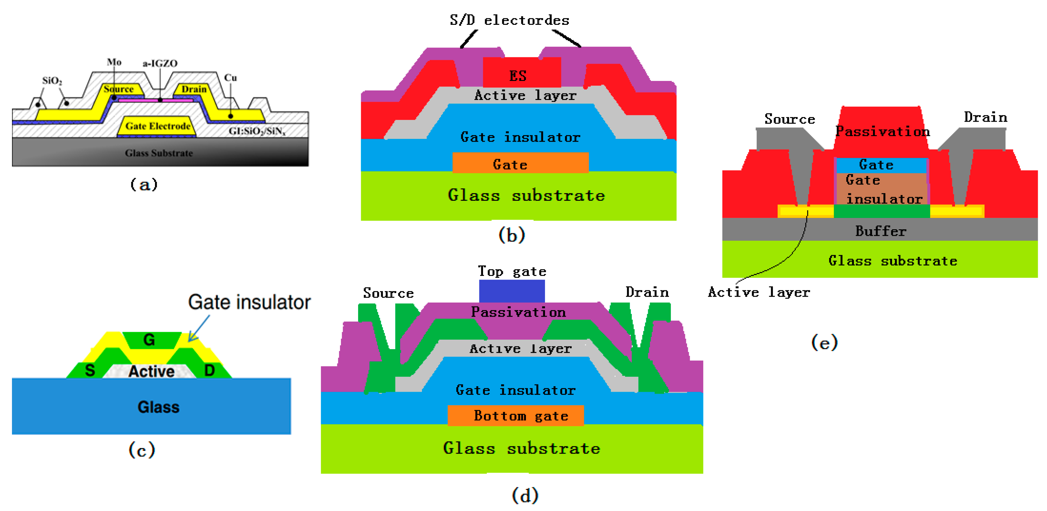
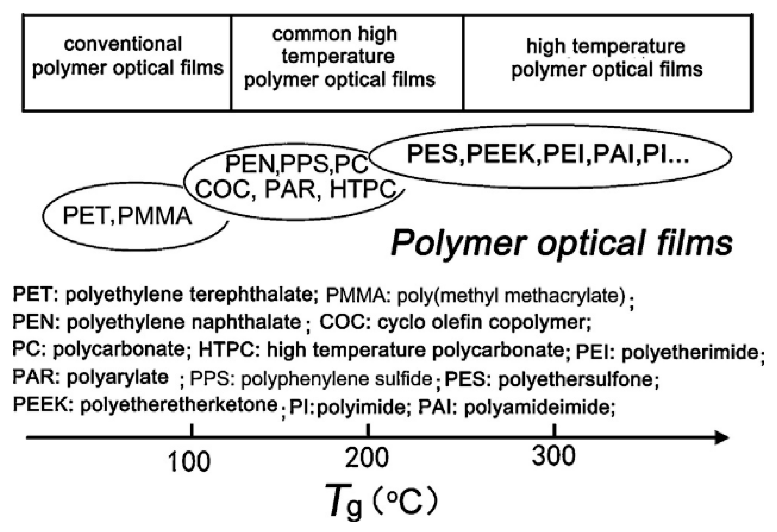
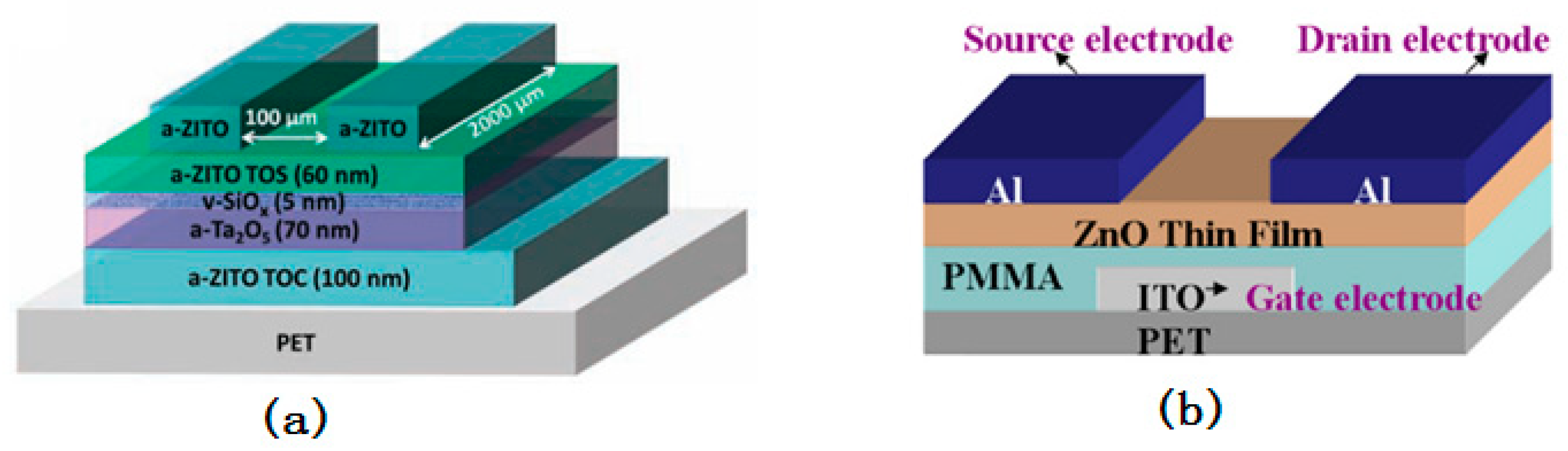
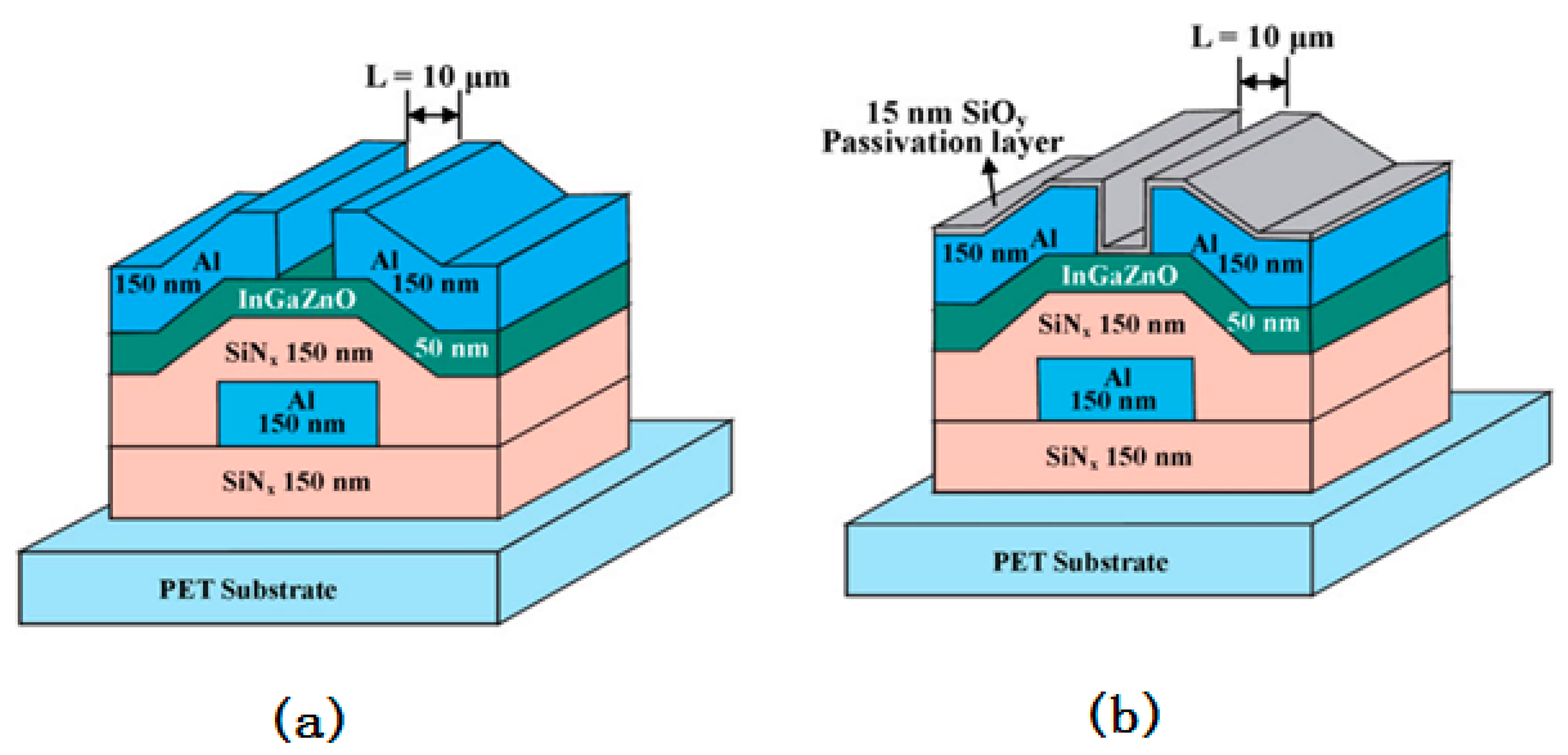
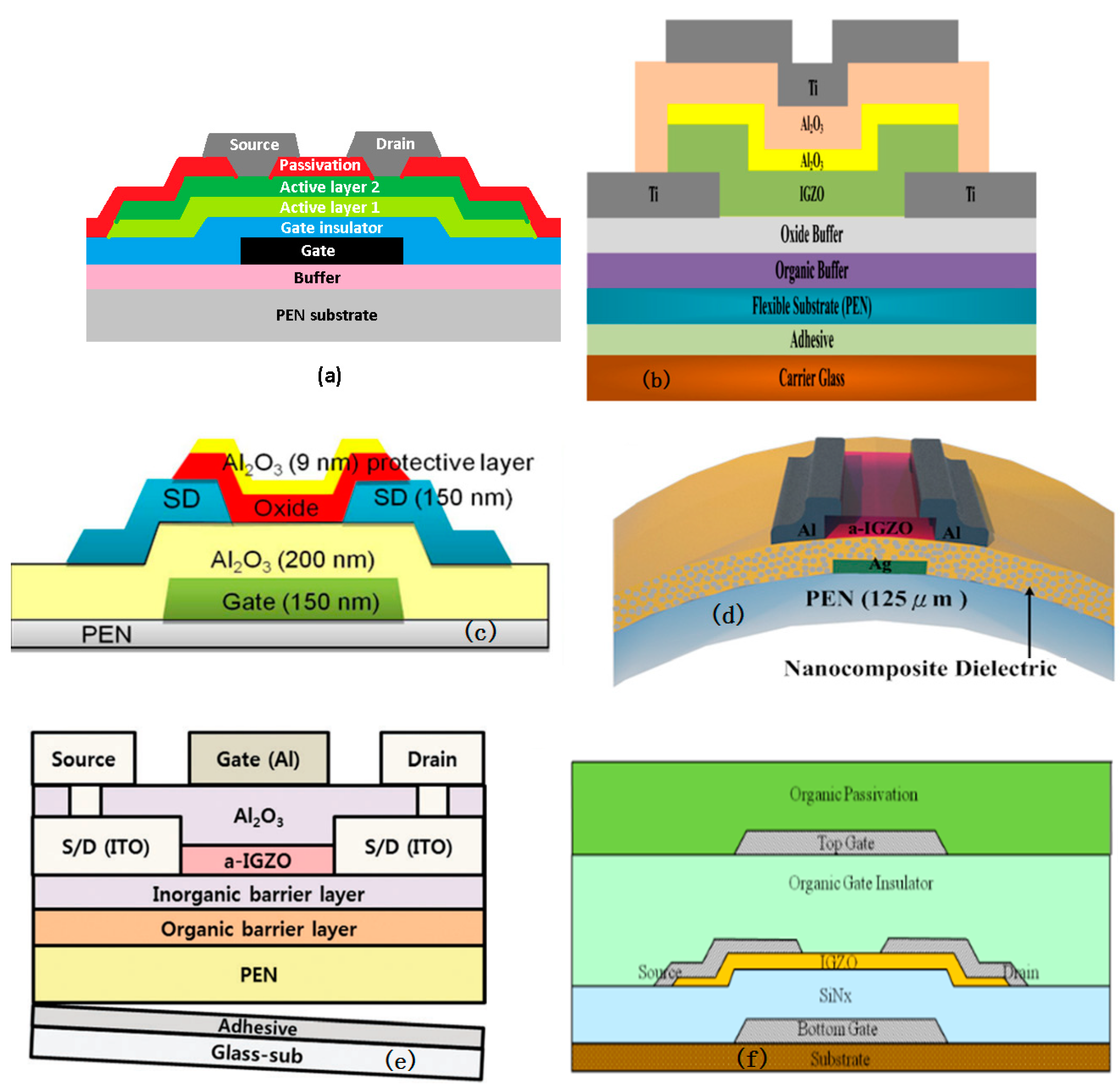
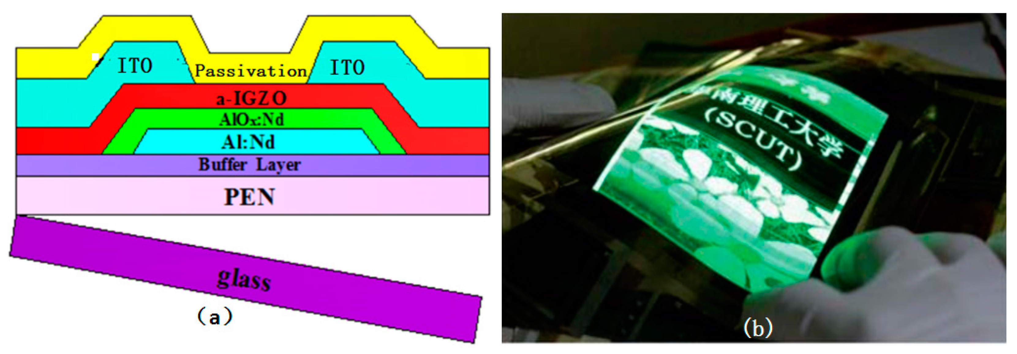
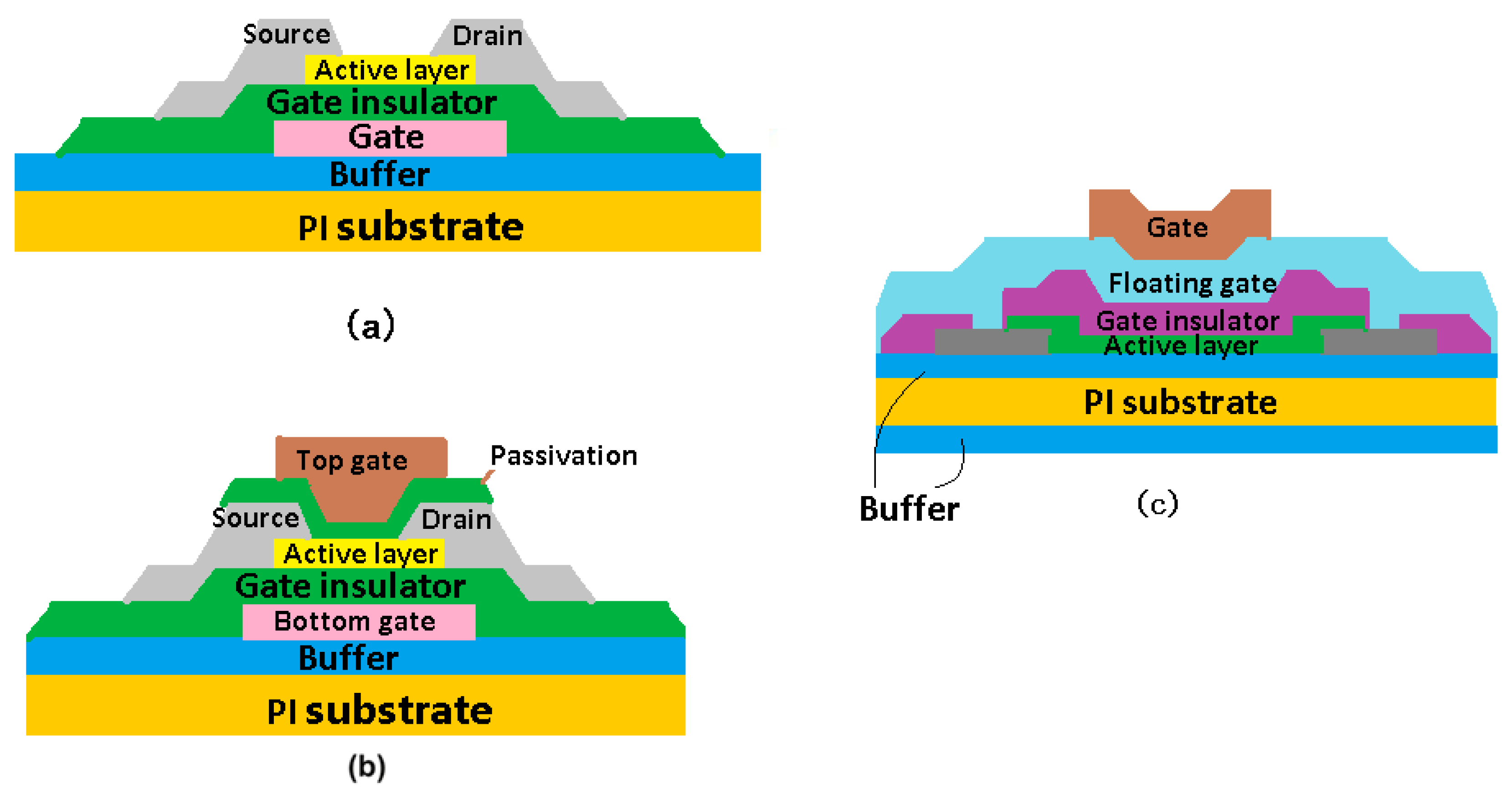
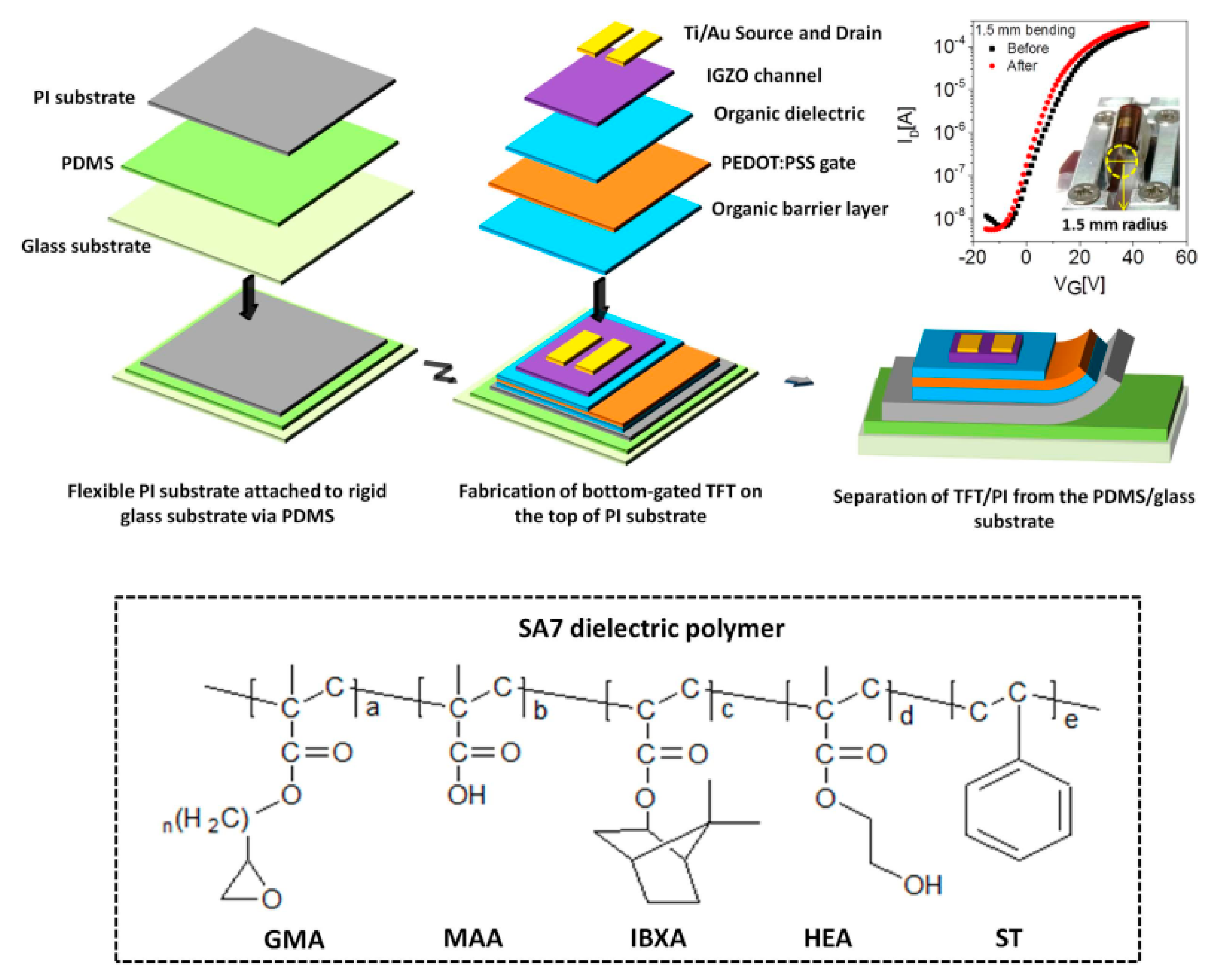
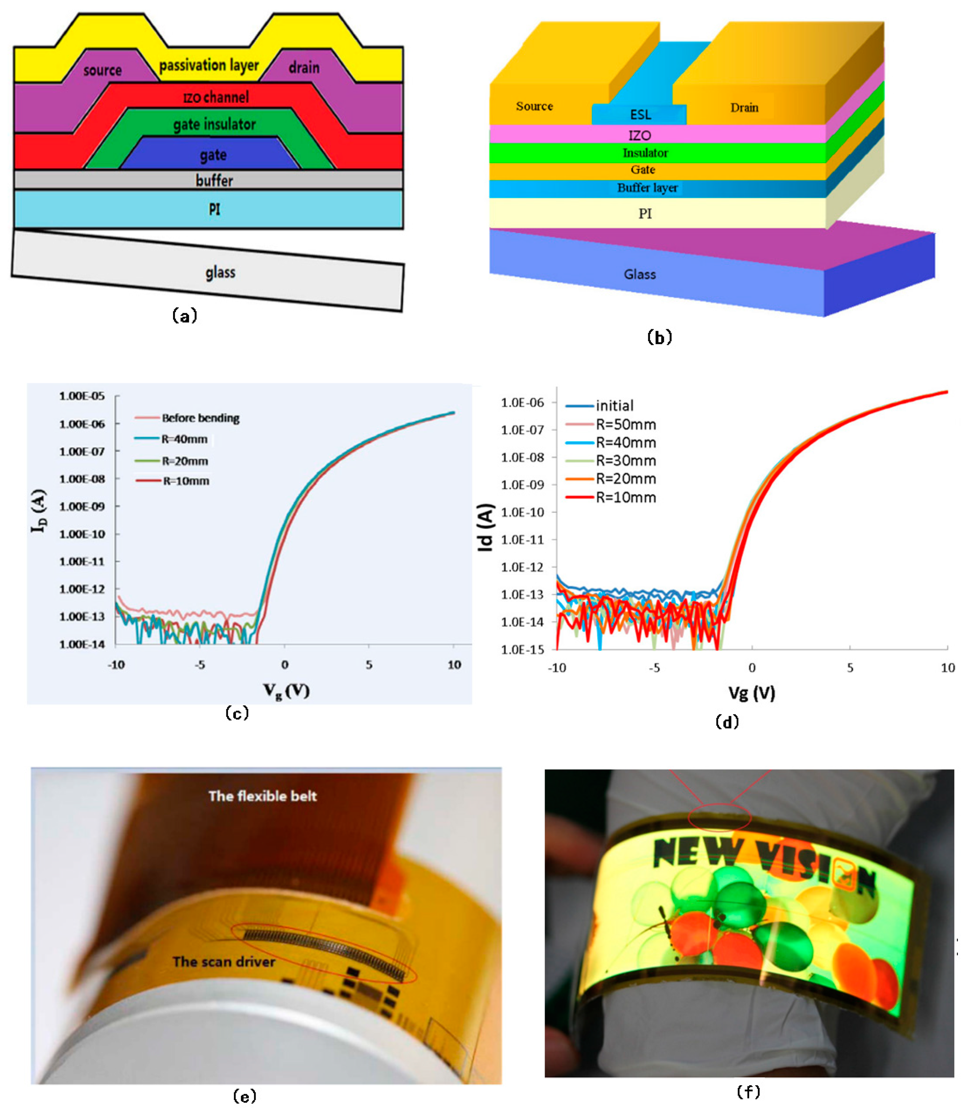
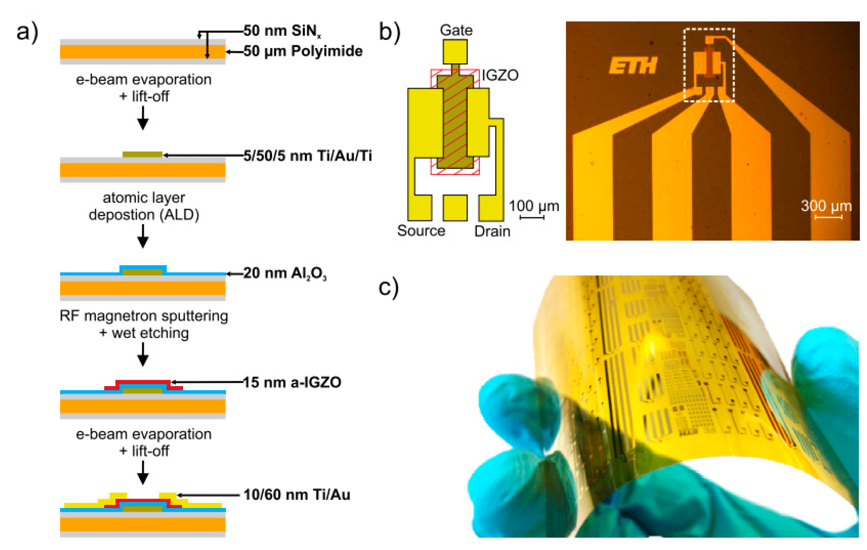
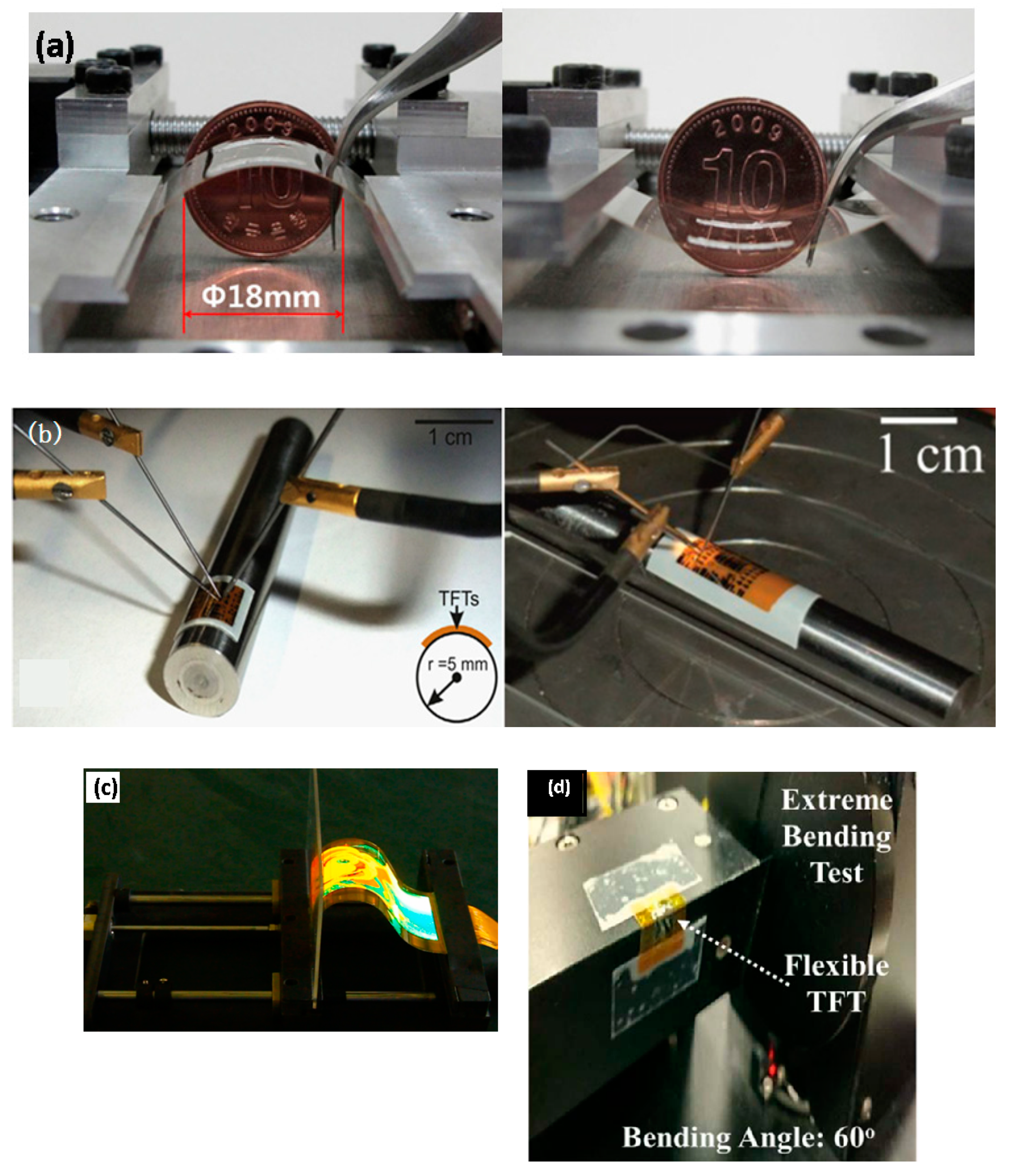
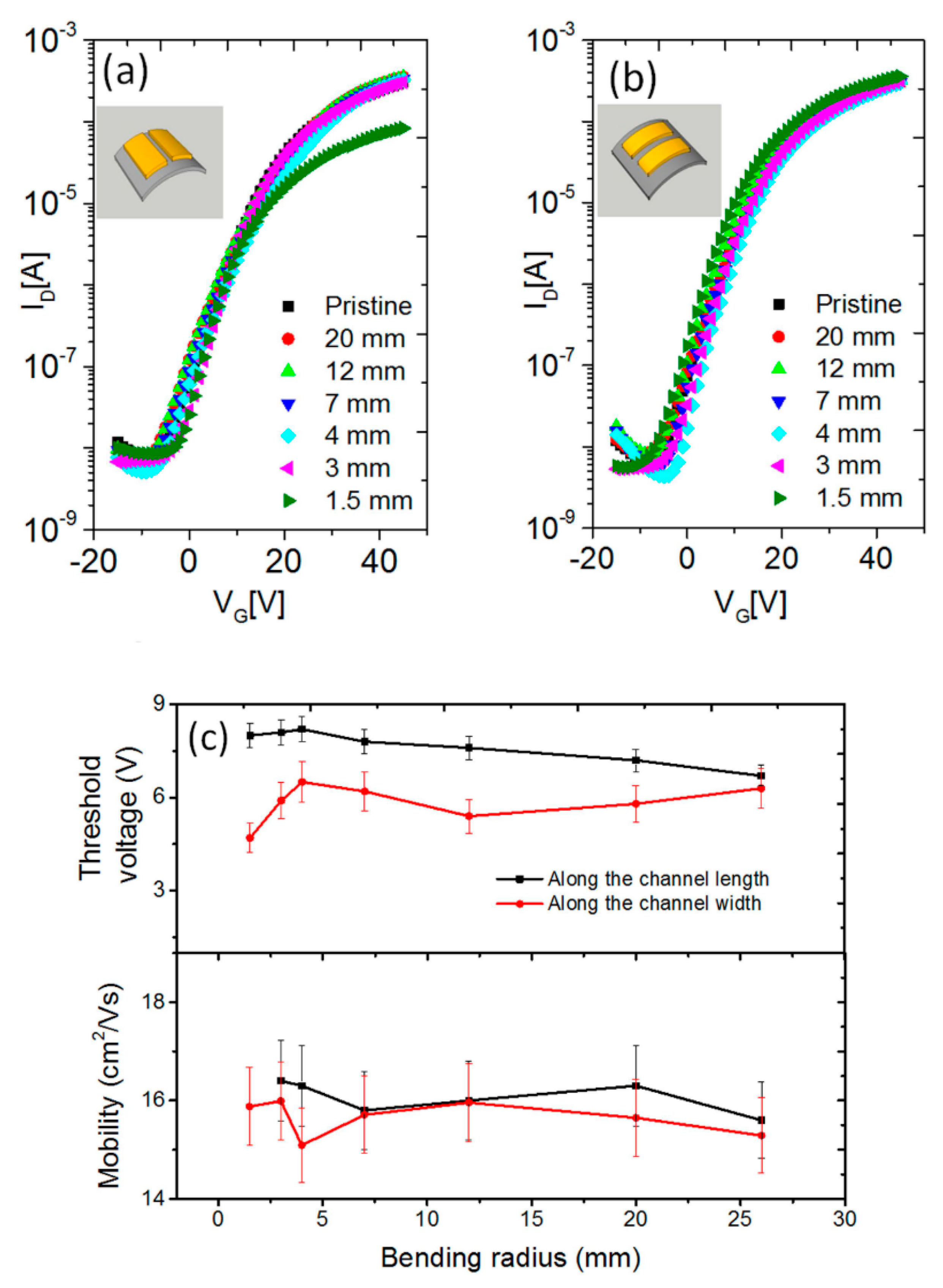
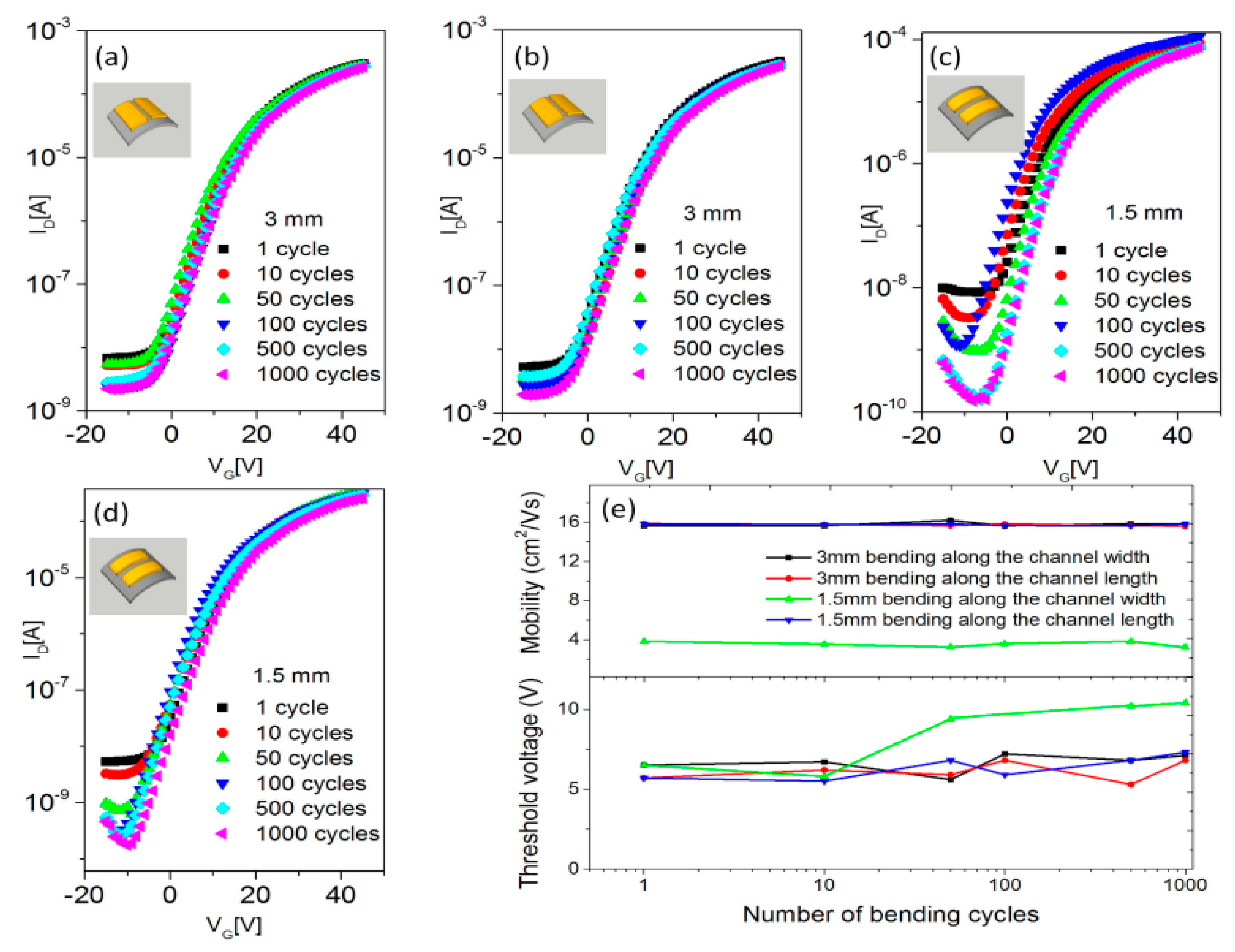
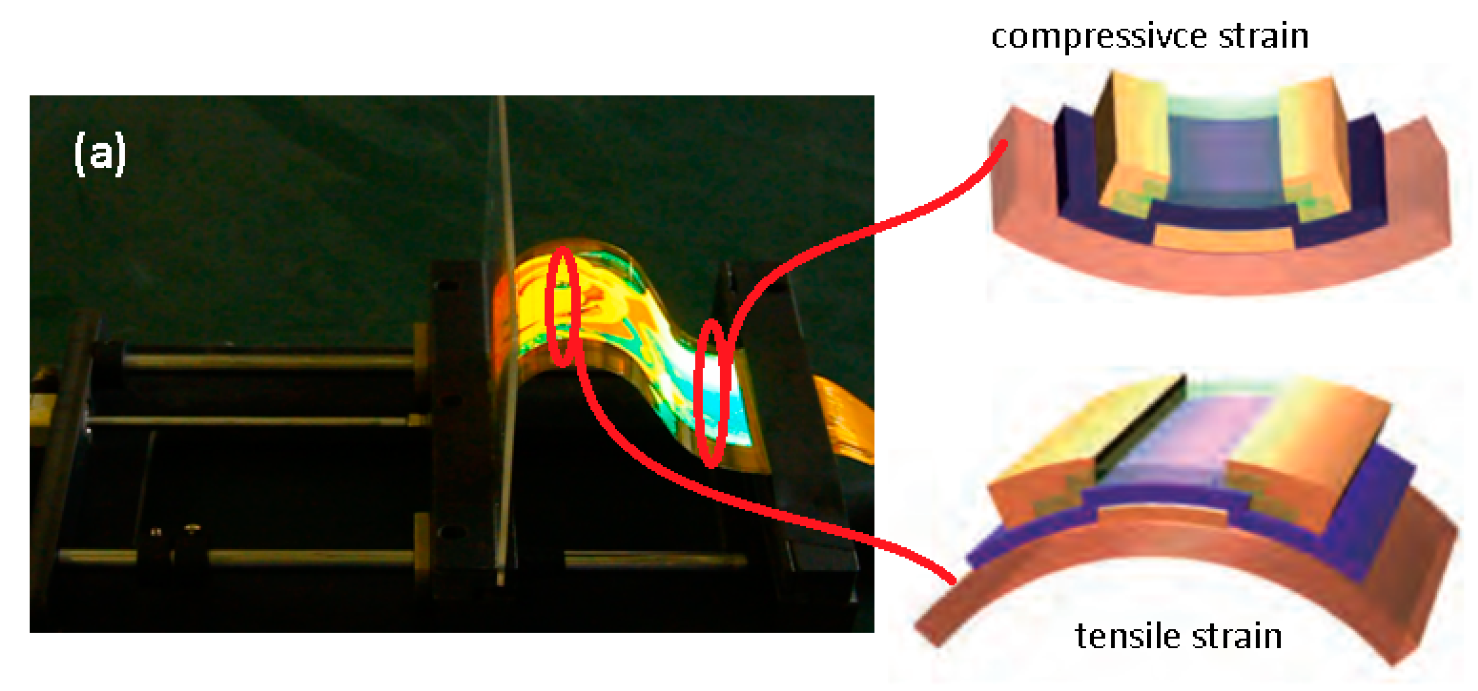
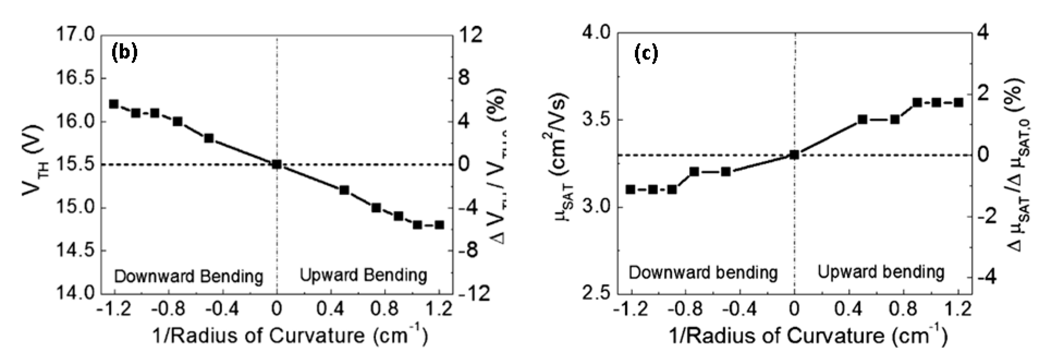
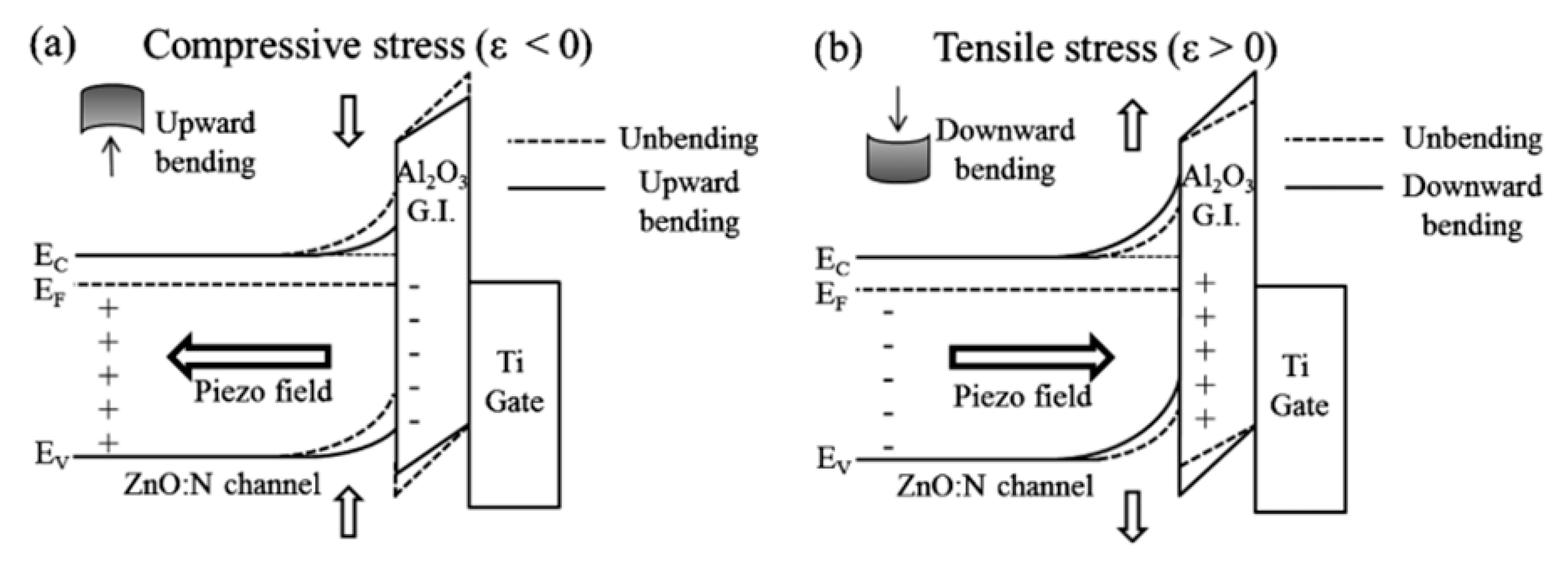
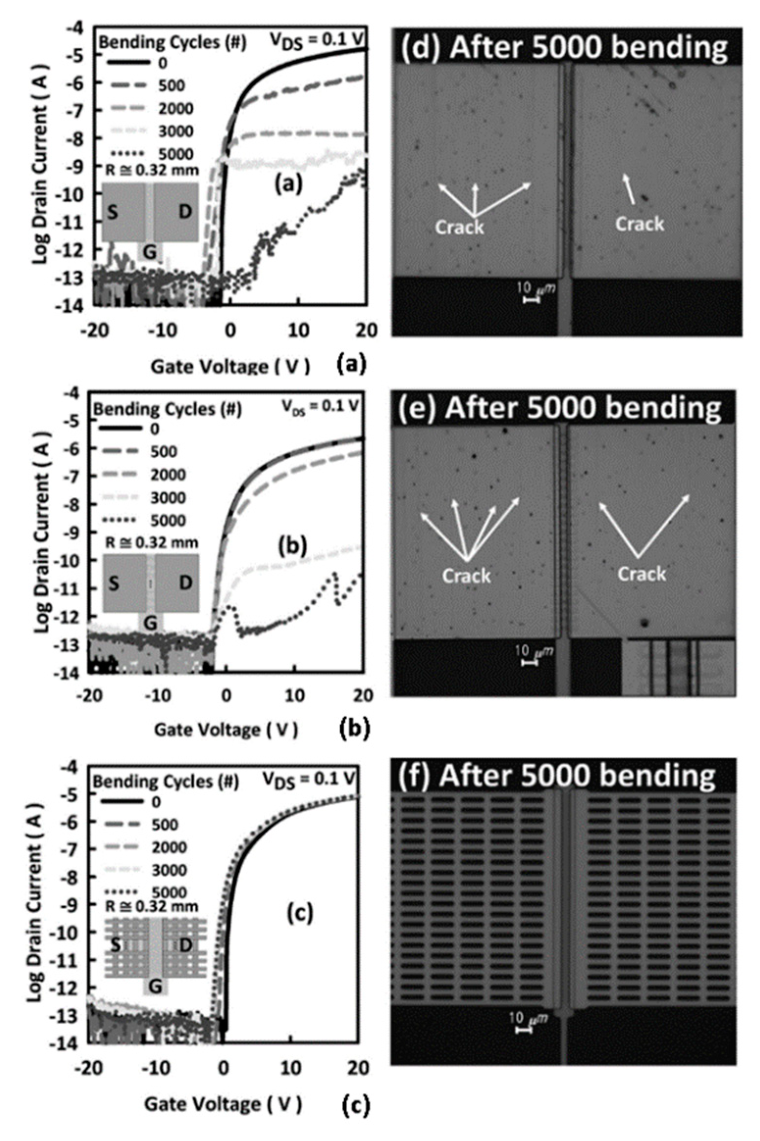
Table 1.
Summarized performances for representative flexible oxide-based TFTs.
| TFTs | Threshold Voltage (V) | Mobility (cm2 V−1 S−1) | On/Off Current | Subthreshold Swing (V dec−1) | Channel Material | Substrate | Temperature (°C) |
|---|---|---|---|---|---|---|---|
| Reference [71] | 4 | 20 | 105 | 0.26 | a-ZITO | PET | <150 |
| Reference [69] | 5.4 | 7.53 | 104 | >2 | ZnO | PET | <150 |
| Reference [150] | 1.3 | 21.3 | 2.7 × 10⁷ | 0.23 | AZO | PET | room temperature |
| Reference [151] | 2.85 | 8.0 | 2.51 × 10⁷ | 0.23 | InGaZnO | PET | - |
| Reference [57] | 1.2 | 66.7 | 2 × 10⁷ | 0.33 | TZO | PET | 80 |
| Reference [86] | 1.93 | 7.83 | ~108 | 0.24 | IGZO | PEN | 150 |
| Reference [124] | 5.5 | 4.1 | ~108 | 0.2 | IZO:F | PEN | 200 |
| Reference [154] | 4.1 | 15.5 | 2.2 × 10⁸ | 0.2 | IGZO | PEN | 180 |
| Reference [156] | 2.48 | 12.87 | 109 | 0.2 | IGZO | PEN | 150 |
| Reference [157] | 0.1 | 5.39 | 2 × 10⁵ | 0.81 | LZZO | PI | 320 |
| Reference [158] | 0.95 | 10 | 2 × 10⁹ | 0.069 | IGZO | PI | 150 |
| Reference [159] | −0.6 | 9.5 | 4.5 × 10⁸ | 0.109 | IGZO | PI | 150 |
© 2019 by the authors. Licensee MDPI, Basel, Switzerland. This article is an open access article distributed under the terms and conditions of the Creative Commons Attribution (CC BY) license (http://creativecommons.org/licenses/by/4.0/).
Share and Cite
MDPI and ACS Style
Zhang, L.; Xiao, W.; Wu, W.; Liu, B. Research Progress on Flexible Oxide-Based Thin Film Transistors. Appl. Sci. 2019, 9, 773. https://doi.org/10.3390/app9040773
AMA Style
Zhang L, Xiao W, Wu W, Liu B. Research Progress on Flexible Oxide-Based Thin Film Transistors. Applied Sciences. 2019; 9(4):773. https://doi.org/10.3390/app9040773
Chicago/Turabian StyleZhang, Lirong, Wenping Xiao, Weijing Wu, and Baiquan Liu. 2019. "Research Progress on Flexible Oxide-Based Thin Film Transistors" Applied Sciences 9, no. 4: 773. https://doi.org/10.3390/app9040773
Note that from the first issue of 2016, this journal uses article numbers instead of page numbers. See further details here.