Review

Addressing the Theoretical and Experimental Aspects of Low-Dimensional-Materials-Based FET Immunosensors: A Review

by
Ernane de Freitas Martins
1,2,
Luis Francisco Pinotti
3,
Cecilia de Carvalho Castro Silva
4 and
Alexandre Reily Rocha
5,*
1
School of Engineering, Royal Melbourne Institute of Technology (RMIT) University, Melbourne, VIC 3004, Australia
2
Catalan Institute of Nanoscience and Nanotechnology (ICN2), CSIC and BIST, Campus UAB, Bellaterra, 08193 Barcelona, Spain
3
Semiconductors, Instruments and Photonics Department (DSIF), School of Electrical and Computer Engineering (FEEC), University of Campinas (Unicamp), Campinas, São Paulo 13083-852, Brazil
4
MackGraphe—Mackenzie Institute for Research in Graphene and Nanotechnologies, Mackenzie Presbyterian University, São Paulo 01302-907, Brazil
5
Instituto de Física Teórica, São Paulo State University (UNESP), São Paulo 01140-070, Brazil
*
Author to whom correspondence should be addressed.
Chemosensors 2021, 9(7), 162; https://doi.org/10.3390/chemosensors9070162
Submission received: 16 May 2021 / Revised: 15 June 2021 / Accepted: 16 June 2021 / Published: 25 June 2021
(This article belongs to the Special Issue Electrochemical Immunosensor)

Abstract

:
Electrochemical immunosensors (EI) have been widely investigated in the last several years. Among them, immunosensors based on low-dimensional materials (LDM) stand out, as they could provide a substantial gain in fabricating point-of-care devices, paving the way for fast, precise, and sensitive diagnosis of numerous severe illnesses. The high surface area available in LDMs makes it possible to immobilize a high density of bioreceptors, improving the sensitivity in biorecognition events between antibodies and antigens. If on the one hand, many works present promising results in using LDMs as a sensing material in EIs, on the other hand, very few of them discuss the fundamental interactions involved at the interfaces. Understanding the fundamental Chemistry and Physics of the interactions between the surface of LDMs and the bioreceptors, and how the operating conditions and biorecognition events affect those interactions, is vital when proposing new devices. Here, we present a review of recent works on EIs, focusing on devices that use LDMs (1D and 2D) as the sensing substrate. To do so, we highlight both experimental and theoretical aspects, bringing to light the fundamental aspects of the main interactions occurring at the interfaces and the operating mechanisms in which the detections are based.

Graphical Abstract

1. Introduction

There is an urgent need to detect biomarker molecules at low levels to diagnose, at the development stage, several human diseases, particularly various types of cancer. Biosensors are a particular subset of detection devices that can determine the presence of biological and non-biological matter of biological interest, while using biological materials (or materials that mimic bioreceptors) as the active sensing region. This selectivity region is immobilized on a sensible transducer, and the biological response can be converted into an electrical signal [1].
Biosensing is a very active research area that puts together efforts from researchers in different fields. The main reason for that is the complexity of the operation principles and mechanisms of a biosensor. The first biosensor was introduced by the seminal work of Clark and Lyons in 1962 [2], and since then, a number of devices have been developed employing various materials for different applications [3,4,5,6,7,8,9,10,11,12].
Usually, the biomarkers detected by biosensors are proteins, and the specific and sensitive detection of these species can be efficiently performed using electrochemical immunosensors (EI), especially those based on field-effect transistors (FET) [8]. FET-based immunosensors have attracted significant attention because they are an ideal biosensor that can directly translate the interactions between target biological molecules and a bioreceptor (antibody) immobilized on the device surface into readable electrical signals [13,14,15].
In a standard FET, the current flows along a semiconductor material (the channel) connected to a source and a drain electrode. The semiconductor channel’s conductance is modulated by a third (gate) electrode that is capacitively coupled via a thin dielectric layer. Thus, the semiconductor channel is directly connected with the sample solution, giving better control over the surface charge. This implies that FET-based biosensors might be more sensitive to biological events occurring on the surface, resulting in the semiconductor surface potential variation, in turn modulating the channel conductance. An emerging strategy to improve the sensitivity of FET-based immunosensors, allowing the detection of biomolecules at the z-aM range, is to replace conventional semiconductor materials (bulk structures) with low-dimensional ones [16].
Materials with at least one physical dimension at the nanoscale that may exhibit different physical and chemical properties compared with their bulk counterpart are referred to as low-dimensional materials (LDM) [17,18]. LDMs can be classified into three groups based on their dimensionalities: (i) zero-dimensional (0D), which includes quantum dots, fullerenes, and nanoparticles with all the three dimensions at the nanoscale; (ii) one-dimensional (1D), including nanoribbons, nanotubes, nanowires (NWs), nanofibers, and nanorods, with two dimensions at the nanoscale and; (iii) two-dimensional (2D), represented by nanosheets and nanoplates, with one dimension at the nanoscale, such as graphene, transition metal dichalcogenides (TMDs), and black phosphorus (BP), among others [17,18].
The use of LDMs in fabricating FET-based immunosensors can lead to increased sensitivity, lowering their limit of detection (LOD) [19,20,21,22,23,24]. This introduces the possibility of going down to the single-molecule resolution. Besides that, the use of LDMs allows for miniaturization with fast-response sensors, paving the way for developing point-of-care devices.
A number of works attribute the outstanding performance of sensing devices that use LDMs as the substrate/transducer element to the high surface area to volume ratio in those materials [25,26,27]. Although that attribute is one of the main reasons for the success of sensors based on LDMs, there is still a lack of complete understanding about the operation principles and mechanisms of FET-based immunosensors on 1D and 2D materials (LDM). Nevertheless, complex systems such as these can present a number of different interplaying phenomena. Thus, a deeper understanding of the underlying mechanisms of FET immunosensors based on LDMs is vital in rationalizing the results and improving the sensing platforms’ performance.
In this review, we assess the most recent theoretical and experimental works on FET immunosensors based on LDMs. Our focus is on FET devices that use 1D or 2D materials as substrate/transducer elements. We will explore the fundamentals of EIs and how a FET can be used as an immunosensor to the benefit of integrating LDMs in FET-based immunosensors. The correlation between the theoretical and experimental works will be highlighted, bringing into light the operation principles and mechanisms of LDM-based FET immunosensors.

2. Fundamentals

2.1. From Biosensors to Immunosensors: Definitions and Type of Transduction

A biosensor is usually composed of three components: the biological recognition system (bioreceptors), the transducer, and the signal processor. The biological recognition system translates information from the biochemical domain, usually the concentration of the target analyte, into a chemical or physical output signal, with a very well-defined sensitivity. The purpose of the recognition system is to provide selectivity for the analyte to be measured. The transducer is used to transform the bio-recognition signal (electricity, heat, mass change, etc.) into another one that varies according to the type of transducer employed: electrodes, thermistor, and piezoelectric devices, for instance. Finally, the signal processor is used to change the detected signal into one that can be interpreted in a meaningful way [28,29,30].
Biosensors can be classified into two types, based on their sensitive element: catalytic or affinity. Catalytic biosensors employ enzymes, cells, or tissue slices immobilized on the surface [31,32,33,34]. Affinity biosensors, on the other hand, are based on a strong and specific interaction and employ the antigen/antibody complex, DNA, or RNA [35,36]. Biosensors that use the specific antigen/antibody immunoreaction receive another designation: immunosensor.
In an immunosensor, either antibody (Ab) or antigen (Ag) can be immobilized on the transducer surface, and the sensitivity is based on the binding strength of the Ag/Ab complex. The interaction between the Ab/Ag is converted into a measurable signal by the transducer, allowing real-time monitoring on the surface. The most prominent advantage of these biosensors is the high selectivity of the immunorecognition event [35,36,37]. Biosensors can also be classified according to the type of transducer as: optical (surface plasmon resonance—SPR, luminescence, fluorescence), piezoelectric (quartz crystal microbalance—QCM), calorimetric, and electrochemical (amperometric, potentiometric, impedimetric or capacitive, voltammetric).
Optical immunosensors are based on the generation of an optical signal (color [38,39,40] or fluorescence [41,42,43]) or upon changes in the local optical properties (absorption or emission of light, refractive index, etc.) after the Ab/Ag complex formation. A photodetector collects the signal, converts it into an electrical signal, and processes it to be analyzed by the user. The most utilized optical immunosensors are based on the SPR phenomenon [44,45]. In piezoelectric immunosensors, on the other hand, physical or mechanical changes are converted into an electrical signal.
The main piezoelectric sensor is the QCM [46,47], which detects changes in the frequency of the crystal’s vibration upon changes in surface mass (Ab/Ag binding) [48]. These crystal oscillations are very stable and precise, making this type of immunosensor extremely sensitive. Finally, calorimetric immunosensors can be applied whenever the immunoreaction is accompanied by heat change. That sensor allows for monitoring the reaction, which is hard to do with other methods [49,50].
An EI is a class of biosensors based on antigen/antibody immunoreaction (sensitive/specific element), where electrodes (transducer) are used to detect electrical changes (bio-recognition signal) in the device. EIs possess several advantages in relation to the previously discussed transductors due to their versatility, portability, high feasibility of miniaturization, fast response, high sensitivity, and the fact that they are generally disposable and less expensive than most other transduction technologies, and can carry out in situ or automated detections [35].
A type of EI that can determine analytes at extremely low concentrations, due to its intrinsic features—such as acting as amplifiers and allowing the highly sensitive detection of non-electroactive biomolecules—is the FET. An FET device is built using semiconductor materials where an electric field modulates the charge carriers in the employed material. The use of this platform to detect immunocomplex formation presents many advantages, mainly because most of the biological components are charged. Thus, the Ag/Ab bond can alter the devices’ charge carriers, changing the current flow and enabling the detection.
To have a clearer view of how an FET can be used as an immunosensor, one first needs to understand the operation principle of the solution-gated FET (SGFET) and how this can render the sensing of biomolecules in liquid samples. In this manner, the SGFET will be discussed in what follows.

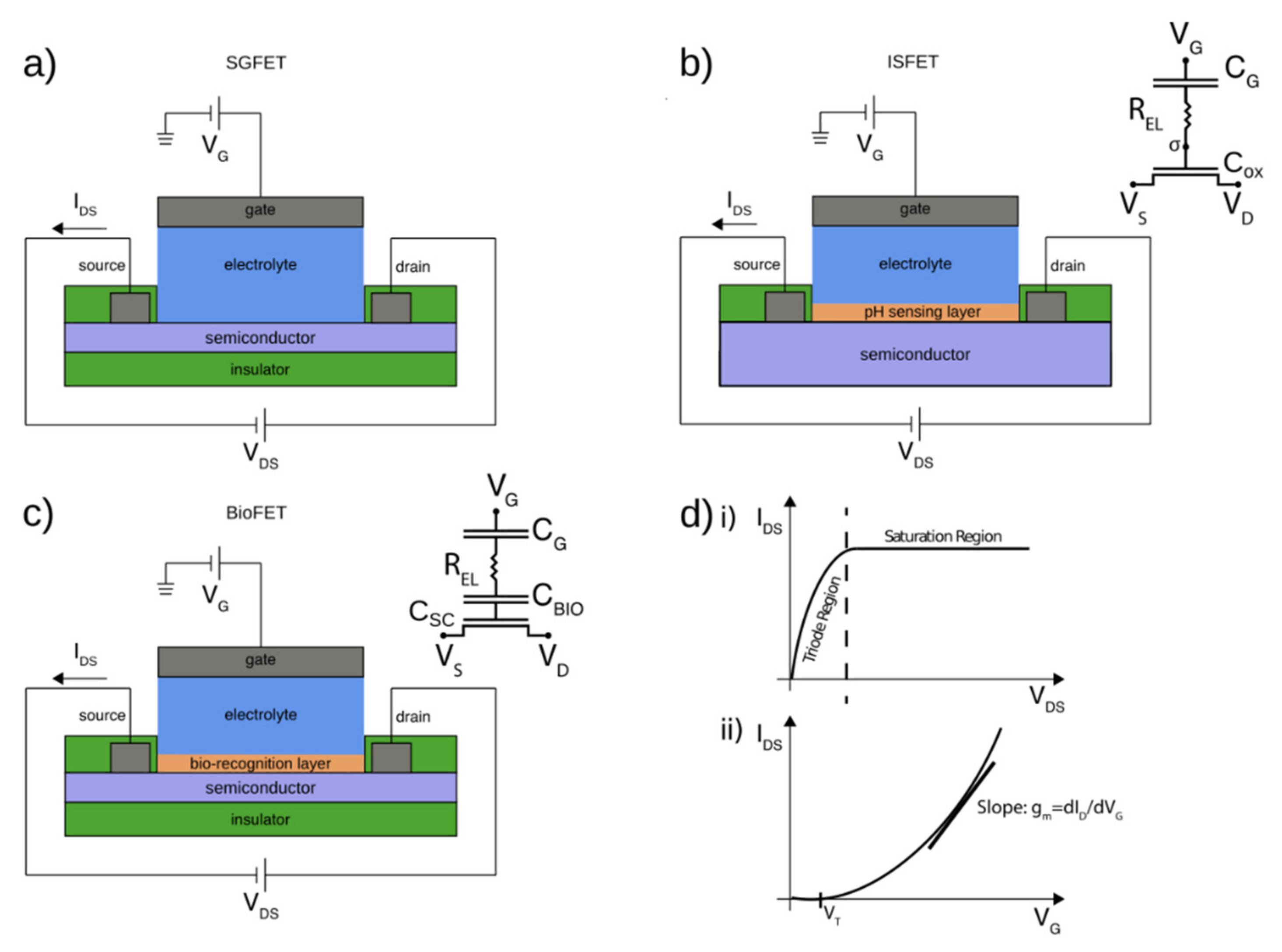
2.2. Field-Effect Transistors as Biosensors—Principles of Operation

SGFETs (Figure 1a) are transistors modified to operate with an ionic solution as the gate. Due to the different possible applications, one can separate them into groups such as the ion-sensitive field-effect transistor (ISFET) depicted in Figure 1c, and the field-effect transistor-based biosensor (BioFET) shown in Figure 1d. The ISFET, introduced by Bergveld in 1970 [51], has its operation mechanism based on changes in gate voltage (VG) and threshold voltage (VTH) due to the ion concentration changes in the solution. This solution-gate can control the current flow in the device channel, even without any bias applied to the electrode in contact with the solution, due to the difference in the potential between the Fermi level of the semiconductor and the redox potential of the solution (determined by the Nernst equation) [51]. In contrast, the BioFET operates on capacitance changes in the bulk semiconductor and in the region of biorecognition events and on the mobility of carriers. Their architectures rely on the SGFET, with differences arising from the ion-sensing membrane over the semiconductor for the ISFET and bio-functionalized layer in the case of the BioFET. Here we discuss the operation of SGFETs applied to biosensing, which is functionalized to sense protein biomarkers, such as antigens, for applications as immunosensors.
In an SGFET, electrical double-layers (EDLs) are established on the gate/solution and solution/semiconductor interfaces. The EDLs can be modeled as capacitors with very small lengths and which present high capacitance values, thus enabling operation with small values of VG. Due to the formation of these structures, the gate is capacitively coupled to the oxide/semiconductor layers [53]. In 2003, Bergveld reiterated that a reference electrode could be introduced in the gate solution to modulate the gate work function. Hence, the VTH presents another explanation of the sensing mechanism beyond Nernst’s equation [54].
The SGFETs applied to biosensing differs slightly from the ISFET since the pH sensing membrane is replaced by a molecule sensing layer. Here, most of the ionic sensing is eliminated since either the metal gate, semiconductor (in the case of organic or 2D materials), or insulator (in the case of permeable semiconductors) utilized is functionalized with bioreceptors (such as antibodies to the detection of antigens/proteins biomarkers), and the insulator (which provides the sensing membrane to the ISFET) is removed. For example, Figure 2a shows a sketch of an SGFET acting as an immunosensor, where specific antibodies are immobilized on the surface of the semiconductor, and Figure 2b–e show images of LDM-FET-based immunosensors using (b) indium phosphide (InP) NW, (c) single-walled carbon nanotube (SWCNT), (d) graphene, and (e) molybdenum disulfide (MoS2).
As stated before, the SGFET sensing capabilities rely on gate capacitance changes, the channel material carrier mobility, and the interfacial potential induced by the biorecognition event between the bioreceptor and the target analyte (Ab/Ag interaction for immunosensors). The current (IDS) in those devices can be obtained by Equations (1) and (2):
I D S = μ C S C A S C W L V E L V T H V D S   if   V G > V T H   and   V D S V E L V T H   Linear
I D S = μ 2 C S C A S C W L V E L V T H 2   if   V G > V T H   and   V D S > V E L V T H   Saturation
where W is the width of the channel, L is the length, μ is the mobility of the charge carriers in the channel, CSC is the capacitance of the electrolyte-semiconductor portion of the device, ASC is the semiconductor area, VEL is the potential in the bulk of the electrolyte, VG is the gate voltage, VTH is the threshold voltage, and VDS is the drain-source voltage. Picca et al. [59] derived these equations for the SGFET based on organic semiconductors, which can be used in the same manner for LDMs and bulk inorganic materials. We reference their work for a complete derivation of the equations and the interplay between the sensing mechanisms and equation parameters. The characteristic curves of the SGFET are presented in Figure 1d, output (i) IDS vs. VDS and transfer (ii) IDS vs. VGS. Basically, from the transfer curve, it is possible to analyze specific changes introduced due to recognition events and quantify the concentration of analytes, exploring for example alteration in the transconductance ((gm) slope of the transfer curve, Figure 1d(ii)), VTH and charge carrier mobility values.
BioFETs have been explored to detect different species, such as protein biomarkers and pathogens [8,15]. These devices are manufactured using conventional bulk semiconductors, such as silicon [60] and indium oxide [61], or organic semiconductors materials such as pentacene [62], α-sexithiophene [63], and P3HT [64], among others [52]. However, the need to detect ultra-low concentrations of target analytes requires the search for materials that possess high charge carrier mobility and surface chemistry that allows for the immobilization of a higher density of bioreceptors. In addition to that, due to the advent of printable electronics, and the possibility to develop flexible and disposable BioFETs, flexible semiconductor materials that have good electronic properties and high chemical stability—features not offered by the traditional semiconductors—become increasingly needed.
In this scenario, BioFETs based on LDMs arise as candidates to enhance the sensitivity of such devices, enabling the possibility of going down to single-molecule resolution. Besides that, LDMs offer several advantages in relation to bulk semiconductors, such as a decrease in response time, higher electrical sensitivity to the binding of the analytes on the antibodies, and the prospect of developing flexible FET immunosensors. In that sense, it is crucial to determine the properties of the LDM to use it in the rational design of immunosensors that can meet the user’s needs in the detection of target analytes.

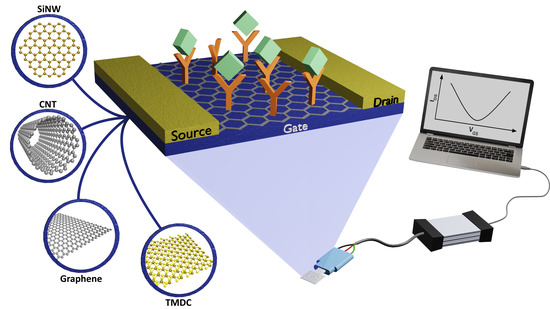
2.3. LDM Semiconductors in FET-Based Immunosensors

Here we mainly focus on the semiconductor features of 1D and 2D materials that are important for applications in FET-based immunosensors. As for 0D materials, metal nanoparticles have been extensively explored to decorate the surface of 1D and 2D materials aiming to promote the amplification of the detection signal, improving the sensitivity of the devices [65], as will be discussed in this review.
Many LDMs exhibit exceptional features, such as a large surface-to-volume ratio, atomic-level thickness, versatile surface chemistry, bandgap tunability, outstanding electrical conductivity and charge carrier mobilities, flexibility, and transparency, that are distinct from their 3D bulk counterparts [66]. Table 1 summarizes some of the unique features of the most popular 1D and 2D materials used to develop FET-based immunosensors. Those features are directly related to the successful development of highly sensitive and robust FET-based immunosensors. For example, due to their high surface-to-volume ratio, most of the atoms are on the surface. In the extreme case of graphene, all the carbon atoms are on the surface. In this way, these materials could show unprecedented levels of sensitivity to the surrounding environment. Furthermore, changes in their electrical properties (conductance) due to chemical or biological interactions are amplified in relation to the bulk [25].
Moreover, the high surface area of LDMs allows for a higher density of bioreceptors to be immobilized on their surfaces since more active sites will be exposed to interact with the bioreceptors. That results in FET-based immunosensors with improved sensitivity and extremely low LOD, reaching unequaled detection levels of zM [16].
The LDM surface properties are deeply related to these materials’ chemical stability, biocompatibility, and the feasibility of functionalizing their surface for improved bioreceptor binding. For example, as they are made entirely of carbon atoms, graphene and carbon nanotube (CNT) present a biocompatible surface to immobilize a wide range of bioreceptors [67]. On the other hand, BP is extremely unstable to the environmental conditions due to its fast oxidation in air and in an aqueous solution [68], which makes the immobilization of the bioreceptors directly on its surface unfeasible, but it can be achieved by other means [21].
Another exciting feature of some LDMs is their high electrical conductivity. Compared to silicon-based FET, several of them present quasi ballistic transport at low voltage, such as SWCNTs. In this way, the working voltage (VDS) necessary for an FET-based immunosensor to operate is extremely low—between 10 mV and 1 V [69]. Low operational VDS values are essential to guarantee the integrity of the antibodies immobilized on the surface of the LDM since high voltages could promote their denaturation and degradation. Furthermore, the development of portable and wearable FET-based immunosensors is benefited by low VDS, since batteries with lower energy density can be used.
One of the most outstanding features of LDMs is the high charge carrier mobility values achieved by some of these materials. The carrier mobility characterizes how rapidly carriers move under an applied electric field in an FET device [27]. The high electrical sensitivity to analyte binding of LDMs in FET-based immunosensors is also deeply related to the high mobility values of their charge carriers, which is fundamentally related and extracted via the transconductance of the device. In this way, the use of materials with higher electrical mobility improves the transconductance signal. This is an essential feature since, in a biorecognition event, the introduction of the target analyte can alter the transfer curve (slope) transconductance (Figure 1d(ii)) by introducing additional scattering sites and hence increasing the disorder [70]. This affects the charge carriers’ mobility values, which result in a change in the transfer curve slope of FET-based immunosensors. As follows, by maximizing the material mobility, the sensing active area, and the capacitive coupling between the semiconductor channel material and the EDL, it is possible to minimize the signal noise and improve these devices’ sensitivity [71].
Additionally, LDMs present a variety of bandgap values, and it directly affects the ION/IOFF ratio—the ratio of the output currents in the ON state and the OFF state—in FETs [27]. LDMs that present high bandgap values and high ION/IOFF ratio have low leakage current values from the gate in an FET, improving the electrostatic gating effect and carrier modulation [72]. Conversely, LDMs with low or no bandgap present a low ION/IOFF ratio. For example, graphene usually offers lower carrier modulation than MoS2 in a FET-based immunosensor [58]. Finally, another significant feature of LDMs is that they intrinsically have the same size as the target biomolecules. This size compatibility paves the way for detecting single-molecule events [13].

2.4. FET Based on 1D and 2D Materials: Detection Mechanisms

As extensively reported in the literature, the high surface area available in LDMs paves the way for surface functionalization, allowing for increased coverage. Nonetheless, comprehending such sensors’ underlying mechanisms of operation is vital in proposing new and more efficient devices. For FET EI devices, we highlight the following main mechanisms: charge transfer, scattering of charge carriers, molecular doping, and changes in EDL.
The charge transfer mechanism is essential for the cases where the detection principle is based on electric changes due to the adsorption of bioreceptors on the LDM employed as a transducer surface. Therefore, when charged species are placed close to the material’s surface, their electronic properties may be altered, and that change can be converted into a measurable signal (resistance, conductance, etc.). However, for FET immunosensor platforms, one usually attaches Ab onto the LDM surface, and the detection signal is measured after the Ag is added, forming the immunocomplex. In that sense, the new charges added in the system due to the presence of the Ag could be far from the surface, hindering the detection based on charge transfer, especially when large Ab/Ag is used.
Another primary detection mechanism in FET-based immunosensors is the scattering of charge carriers, which is also related to the charge transfer mechanism. The presence of either chem- or physiosorbed (macro) molecules onto the LDM surface may act as new scattering centers. Similar to having defects in those materials, the charge carriers in the conducting channel will be affected, leading to modifications in the electrical signal [95]. The polarity of the added scattering sites will influence the charge carriers (holes or electrons). The transfer characteristics curve slopes (the transconductance) will vary, often asymmetrically, indicating that the biorecognition event occurred [70].
Molecular doping is often explored in sensing platforms since the type of semiconductor material employed in the FET immunosensor will determine the device’s conductivity trend. If, on the one hand, one uses p-type materials, i.e., materials where the carriers are “holes”, a decrease (increase) in the conductivity is observed for a positive (negative) gate voltage. If, on the other hand, one uses an n-type material, i.e., materials where the carriers are electrons, an opposite trend in the conductivity is observed [14]. Molecular doping is often observed by analyzing the shift in VTH in the transfer characteristics curves when adding the analyte [96].
Changes in the EDL are also considered a critical operating mechanism of FET-based immunosensors. Once the EDL is formed at the electrolyte/LDM interface, biorecognition events occurring at that region will lead to changes in the EDL capacitance. In this manner, that change can be detected in the device, providing a measurable signal. However, the EDL can also lead to screening of the analyte’s charge when detecting charged systems in a sample that contains a solution with high ionic content, since the ions in the EDL region may interact with the analyte [97].
In SGFET devices, for instance, an EDL is formed with or without an applied voltage bias applied, when an electrolyte solution, such as a biological fluid, is in contact with the semiconductor surface. The EDL is composed of electrolyte ions with opposite charges from the carriers accumulated on the semiconductor surface. Its effective length is measured via the Debye length (λD), which is inversely dependent on the square root of the ionic strength (I) of the solution [14]:
λ D = ε k B T 2 N A e 2 I   ,
where ε is the dielectric constant of the electrolyte multiplied by the vacuum permittivity, kB is the Boltzmann constant, T is the temperature of the electrolyte, NA is Avogadro’s number, e is the electron charge, and I is the ionic strength of the electrolyte.
Thus, the higher the concentration of ions in the solution, the shorter λD consequently the EDL is formed closer to the semiconductor surface. Hence, when a biorecognition event occurs within λD, the changes in the charges due to that event can be sensed by the device. Otherwise, if the event occurs further away from λD, the interaction is screened out, which ends up causing the loss of sensitivity of the BioFET.
Depending on the LDM employed, the operating mechanism on which the bio-recognition event is based may change. In the following, we describe the most recent works on EIs based on LDMs, highlighting the underlying detection mechanisms and correlate theoretical and experimental works when possible.

3. Recent Applications towards Biosensing

3.1. 1D Materials

3.1.1. Carbon Nanotubes

One of the quintessential representatives of a one-dimensional system is the CNT. A CNT corresponds to a cylindrical structure made entirely of carbon atoms formed by rolling a single sheet of graphene. First discovered by Iijima in 1991 [98], CNTs can be either metallic or semiconducting depending on chirality and radius. They can also appear as SWCNT or multi-walled nanotubes (a number of concentric SWCNTs of different radii) [99]. This confers a range of possibilities that combines low dimensionality and different electronic properties. Since the first carbon nanotube field-effect transistor (CNT-FET) device was reported in 1998 by the Avouris group [100], this device has been explored in different types of sensing applications (gas [101], ions [102], proteins [103], nucleic acids, [104,105] and in immunosensing [13,56,106,107]).
Semiconducting (sc) SWCNTs possess outstanding properties for developing highly sensitive FET-based immunosensors, such as high on-state conductance and high ION/IOFF ratio. These properties provide higher analytical sensitivity toward the target analyte than other carbon nanomaterials such as unsorted SWCNT and graphene [106]. However, one of the challenges related to using SWCNTs as FET immunosensors is related to the mixture of SWCNTs with metallic and semiconducting properties obtained during synthesis. Nonetheless, nowadays, high-purity sc-SWCNTs are commercially available, albeit at a high cost [108].
Recently, Shao et al. [106] showed the use of sc-SWCNTs in the development of FET-based immunosensors to detect the spike (S) and nucleocapsid (N) proteins for the severe acute respiratory syndrome coronavirus 2 (SARS-CoV-2) with very high sensitivity, reaching an LOD of 0.55 fg/mL for S and 0.016 fg/mL for N, respectively, in deionized (DI) water. The authors used the conventional dielectrophoresis (DEP) method to immobilize the sc-SWCNTs between the S and D electrodes. To immobilize the antibodies against the S and N proteins, the authors took advantage of the residual carboxylic groups on the surface of the sc-SWCNTs, and the very well-established chemistry between the EDC/sulfo-NHS solution [109] to activate the carboxylic groups and bind the antibodies by the amino-terminal groups. The exposed areas of the nanotubes were blocked with a blocking buffer (0.1% Tween 20 and 4% polyethylene glycol in PBS) to avoid nonspecific binding. The successful immobilization of the antibodies on the surface of the (sc)-SWCNTs was proven by the shift of the threshold voltage (VTH) toward more negative gate voltages and the decrease in the device conductance in the p-type region in the transfer characteristics curves.
The device’s sensitivity to detect the S and N protein was also investigated by Shao et al. [106] through the transfer characteristics curves. For the detection of the S protein, shifts toward more positive VTH were observed with the increase of the S protein concentration. The authors attributed this effect to introducing the negatively charged biomolecule (isoelectric point of S protein is 6.24) near the sc-SWCNT surface, which induced additional hole carriers, p-type doping the SWCNTs. For N protein detection, the transfer characteristic curves presented shifts toward more positive VTH values with the increase of the N protein concentration, attributed to an electrostatic gating effect. However, in this case, the authors proposed that the sensing mechanism is predominantly related to the neutralization of charged antibodies upon N protein binding due to its positive charge.
Thus, the devices studied by Shao et al. [106] were able to distinguish the presence of the SARS-CoV-2 in patient samples (nasopharyngeal fluid suspended in the viral transport medium). However, it is important to highlight that all the transfer characteristics curves obtained to detect the S and N protein and the analysis of the patient samples were performed using DI water, not in direct contact with the samples. The devices were incubated with the samples for 2 min and subsequently washed several times to perform the analysis. The authors did not show the use of the device for real-time detection nor the use of fluids that mimic realistic sample conditions (high ionic strength content). However, the FET-based sc-SWCNT developed by the authors is an excellent alternative to provide fast diagnosis of the coronavirus disease of 2019 (COVID-19) (2–5 min.) when compared to the other popular methods available, such as reverse transcription-quantitative polymerase chain reaction (rt–qPCr) (24–48 h) and lateral flow antigen tests (30 min) [110].
Hybrid nanostructures based on CNTs and metal nanoparticles have been profoundly explored in the development of ultra-sensitive FET immunosensors [111,112,113,114]. However, it is crucial to understand how the metal nanoparticles improve the sensitivity in this system and how the interactions with biomolecules adsorbed on the surface of metal nanoparticles modulate the electronic properties of the CNTs. This knowledge may be beneficial in predicting the response mechanism of this hybrid immunosensor and promoting the rational design of new immunosensors architectures.
Michael et al. [115] presented an interesting study on the modulation of the electronic properties of FET devices based on SWCNTs decorated with gold nanoparticles (Au NPs) in the presence of the common stress biomarkers, reduced glutathione (GSH), and oxidized glutathione (GSSG). For this purpose, the authors used milder oxidized (ox) SWCNTs to electrodeposit the Au NPs on its surface. Figure 3a shows the device transfer characteristics before and after Au NPs electrodeposition. As can be seen, there is an increase in the device conductance after the Au NPs immobilization. That finding indicates a strong coupling between the nanoparticles and ox-SWCNT, and a direct charge transfer between AuNPs and SWNTs [116].
In the work of Michael et al. [115], both GSH and GSSG are adsorbed on Au NPs through the formation of Au-S bonds. The transfer characteristics of the proposed device show a decrease in the FET conductance as the concentration of GSH (Figure 3b(i)) and GSSG (Figure 3b(ii)) is increased. The authors attributed the consistent drop in the device conductance to the charge transfer from GSH and GSSG to Au NPs and further to the ox-SWCNTs, resulting in a decrease in the concentration of the major carriers (holes) in the ox-SWCNTs.
Michael et al. [115] also presented a density functional theory (DFT) study to confirm the charge transfer hypothesis mentioned above. Figure 3c shows pictorial views of the corresponding charge difference maps performed for GSSG and GSH molecules. The panels shown in Figure 3c(i,iv) represent the charge difference maps for the GSSH and GSH, respectively, at the interface between the molecules and the Au nanocluster. In contrast, the panels shown in Figure 3c(ii,v) show the charge difference maps at the interface between Au nanocluster and ox-SWCNTs. Via the Bader charge distribution analysis performed by the authors, it was possible to conclude that the GSSG and GSH contributed to a net charge transfer of 0.32 and 0.37 e, respectively, from the Au NPs to the ox-SWCNTs.
Finally, Michael et al. [115] also performed the total density of states (DOS) for the GSH (Figure 3d(i)) and GSSG (Figure 3d(ii)) Au-ox-SWCNT hybrid system, together with the contributions of the projected density of states (PDOS) onto the different components of the complex molecule, AuNPs, and ox-SWCNT. The DOS results (Figure 3d(i,ii)) indicate a nonzero electronic contribution above the Fermi level, suggesting a semimetal or metallic system. Furthermore, from the analysis of panels iii and vi of Figure 3c, the authors could confirm that the charge density is delocalized on both SWCNT and Au NP, contributing to the performance of the hybrid system. Thus, this work shows that combining electrical FET characterization and DFT calculations provides a more in-depth analysis of the operation mechanism in FET immunosensor devices.

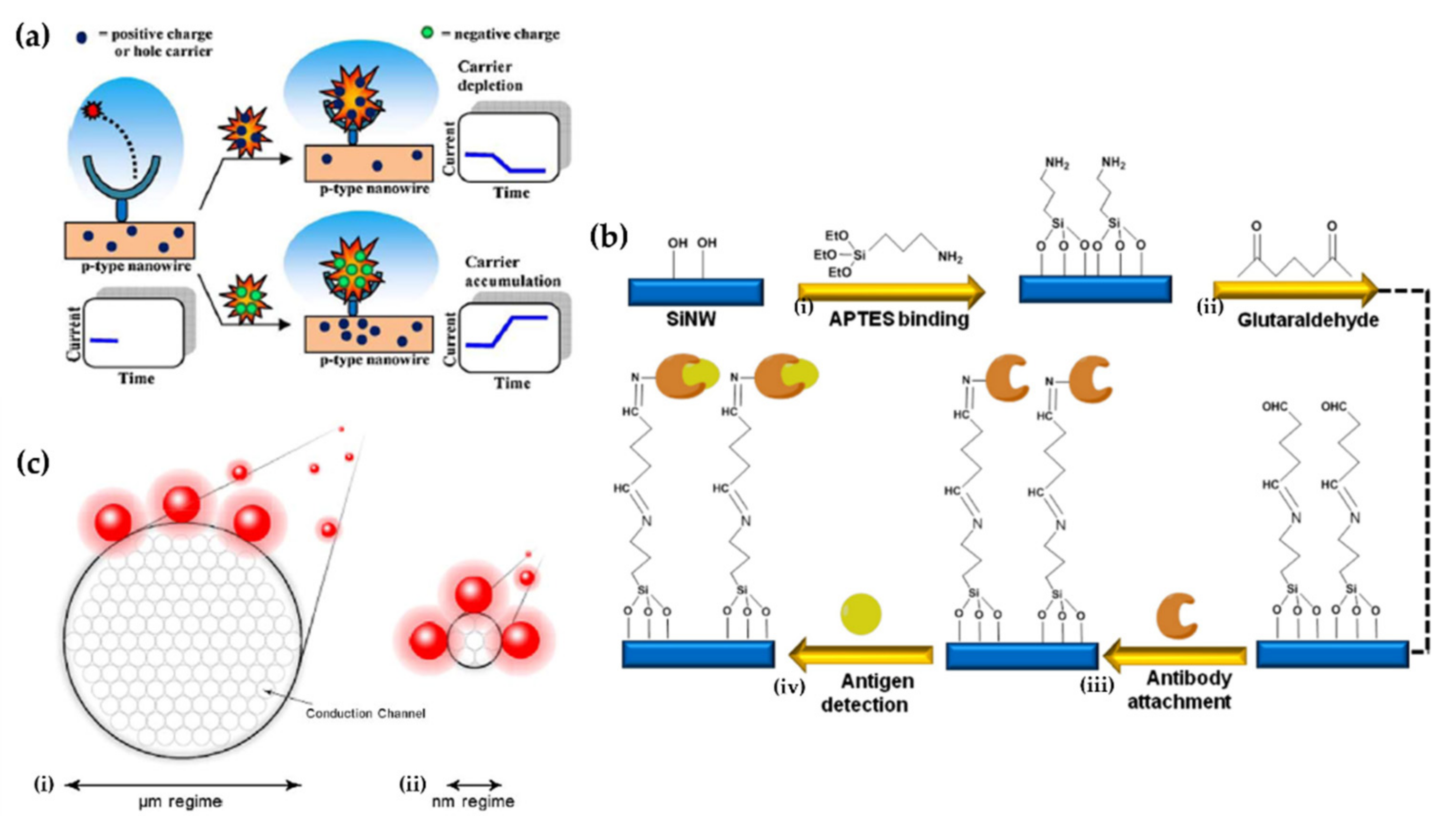
3.1.2. Nanowires—Silicon and Beyond

Different from the hollow structures in carbon nanotubes, semiconducting NWs are compact, with a crystal structure that typically resembles their bulk counterparts [24]. The formation of NWs—usually grown from a metallic precursor—exposes different facets, normally the lowest energy ones [117]. Those different facets can have different reactivity, which can result in selectivity towards different molecules.
In fact, silicon nanowires (SiNWs) are widely used in FET-based biosensors due to their semiconductor properties [88]. The group led by Lieber at Harvard University demonstrated for the first time the use of SiNW-based FETs to sensing streptavidin in the picomolar range [5]. Since then, SiNW-FET-based immunosensors have been extensively explored to detect proteins [118], virus particles [119], and multiple protein biomarkers simultaneously [22,120].
The outstanding electrical sensitivity of SiNW-FET-based immunosensors is related to the high surface-area-to-volume ratio of SiNWs. NWs can behave as 1D quantum wires, with a conductivity that is highly sensitive to minimal perturbations in the surface charge density upon adsorption of molecular targets [121]. In addition, SiNW-FET-based immunosensors benefit from a well-established industrial microfabrication process, where structures can be large-scale-prepared by bottom-up or top-down approaches [88]. Besides that, SiNWs can be doped, in a versatile manner, with positive or negative elements to act as p- and n-type semiconductors, respectively [122].
In general, in a SiNW-FET-based immunosensor, depending on the dominant charge carrier in the nanowire (conductance channel in the FET), the conductance change correlates with the sign of the charges in the target antigen, and the magnitude of the change reflects the antigen-antibody interaction. For instance, for p-type SiNW-FET-based immunosensors (Figure 4a), when the positively charged analytes bind to the immobilized antibody, a depletion of charge carriers occurs in the conductance channel, causing a decrease in the device conductivity. On the other hand, the accumulation of charge carriers in the conductance channel increases the device conductivity.
Proposals of SiNW-FET-based immunosensors are widely reported for cancer diagnostics and monitoring due to their capability for real-time, label-free, and sub-femtomolar detection ranges of cancer biomarkers [88,125]. In this scenario, the work of Tran et al. stands out [126]. First, the authors explored the traditional functionalization of SiNWs with 3-aminopropyl triethoxysilane (APTES) in vapor-phase silanization, enabling a higher homogenization of the surface. Next, the reaction with glutaraldehyde was performed to covalently bind a monoclonal antibody against cytokeratin. Finally, they showed the use of a microchip with arrays (8 channels) of SiNW FETs to detect even a single disseminated tumor cell (DTC) per lymph node, and the presence of circulating tumor cells (CTC) in the blood of colorectal cancer patients as low as 2.5 cells/mL of blood.
Recently, Chang et al. [124] used an approach similar to the one presented by Tran et al. [126] to functionalize the SiNW surface and immobilize a cardiac troponin I monoclonal antibody (Mab-cTnI) (Figure 4b), enabling them to achieve a LOD of 0.016 ng/mL. However, the authors did not investigate the SiNW FET transfer characteristics before and after the immobilization of the Mab-cTnI. That analysis could confirm whether the immobilization of antibodies on the surface of the SINWs was successful by the shift of the VTH.
SiNW-FET-based immunosensors sensitivity is influenced by many factors related to the structure and configuration of the device, such as the NW diameter, doping density, and the number of wires in an FET [127]. For example, Figure 4c shows a schematic representation of the surface-to-volume ratio of a thick (i) and thin (ii) NW. It is possible to see that when charged particles are close to the surface of a thick wire (Figure 4c(i)), the area affected by the electric field exerted from the charged particles is localized on the wire surface. In this way, the atoms located in the interior of the wire are unaffected. On the other hand, when the wire diameter decreases (nanoscale), the influence of the external electric field could reach the entire cross-section of the NW [123]. As one would intuitively assert, this result confirms that the change in conductance in a thinner NW is much more sensitive than in a thicker one.
Li et al. [127] performed a systematic study on the influence of the SiNW diameter, doping density, and the number of SiNWs in the sensitivity of a SiNW-FET-based immunosensor for the model immunodetection of hIgG. The authors demonstrated that the immunosensor sensitivity decreases with the increase of the number of SiNWs deposited between the source and drain electrodes. A device with seven SiNWs per channel presented a reduction of 82% in sensitivity compared to a single NW device. The authors attributed this impressive sensitivity reduction to the competitive binding and depletion of the analytes from the surrounding solution. In this way, the distance between the SiNWs in a multiple-SiNW FET should be very well controlled to achieve a sensitivity comparable to a single-SiNW FET.
In addition, the authors [127] also showed that an immunosensor with a larger diameter (101–120 nm) exhibited a decrease in sensitivity of around 37% compared to devices with diameters of 60–80 nm. A similar feature was observed for the SiNW doping density: higher doping (1019 atoms cm−3) promoted a decrease of the sensitivity of around 69% compared with lower doping density (1017 atoms cm−3). The system with lower doping density is less affected by charge screening due to the mobile charge carriers in the NW, improving the sensitivity of the devices to immunodetection [128]. In summary, these parameters are essential for any NW-FET-based immunosensors, and they should be optimized to ensure higher sensitivity and reproducibility in devices, allowing immunosensors to reach the market.
Besides silicon, other materials have been explored in the development of FET immunosensors based on NWs, such as indium phosphide (InP) [55] and zinc oxide (ZnO) [129,130,131]. In the III-V semiconductor family, InP NWs exhibit exciting features for the development of FET-based immunosensors. For example, InP exhibits lower surface recombination rates and consequently longer carrier lifetimes [132], which undoubtedly improves biosensor performance.
In particular, we highlight the InP-NW-FET-based immunosensor developed by Janissen et al. [55] to detect the Chagas disease protein marker (IBMP8-1). To achieve this, first of all, the authors grew InP NW using chemical beam epitaxy and immobilized them between source and drain electrodes in arrays of FETs, using microfluidic channels. Then, the InP NWs were modified with ethanolamine (EA), followed by poly-(ethylene glycol) (PEG), to bind the specific polyclonal IBMP8-1 antibodies. As a result, the device presented impressive high sensitivity, with a LOD of 5.7 fM for IBMP8-1. Furthermore, the authors claimed that the successful detection of the IBMP8-1 is related to the excellent uniformity in the immobilized receptor on the InP NWs surface and the capture binding performance of the antibodies, since the molecular linker used by the authors (EA plus PEG) decreased the steric hindrance for the antigen (IBMP8-1). Thus, this work brought a significant contribution, showing that the nanomaterials’ functionalization to immobilize bioreceptors plays an essential role in the sensitivity of FET-based immunosensors.
Another material, which shows very attractive properties for the development of high sensitivity FET-based immunosensors, is ZnO. It has low cost, is abundant, non-toxic, compatible with intercellular material, and possesses a large direct bandgap of 3.37 eV, contributing to high ION/IOFF ratios [131]. In this way, ZnO NW (or nanorod (NR), as they are more commonly known) has gained a lot of attention as a semiconductor material for developing FET-based immunosensors [7,133]. One of the distinctions of ZnO NRs is their use to build FET in a non-planar configuration. Chakraborty et al. [130] showed the effect of the horizontal and vertical drain-source contact configuration in the sensitivity of a ZnO-NR-FET-based immunosensor for the ultrasensitive detection of Hep-B antigen biomarkers. First, the authors covalently immobilized the anti-Hep-B monoclonal antibodies on the ZnO NRs surface using the 3-mercaptopropyltrimethoxysilane (MTS). Then, they evaluated the IDS changes in the device transfer characteristics (IDS vs. VDS) curves for the horizontal and the vertical configuration in the presence of different antigen concentrations.
Figure 5b from Chakraborty et al. [130] shows the sensitivity variation as a function of the antigen concentration at 1 MHz frequency for both horizontal and vertical electrode configurations. It is possible to see that the LOD for the horizontal electrode configuration cannot go beyond 1fM. However, in the vertical electrode configuration, the LOD can be reduced by two orders of magnitude down to 0.02 fM with a sensitivity of approximately 20%. Besides that, the sensitivity at 1fM antigen concentration increases by more than 200% in the vertical configuration compared to the horizontal one. The authors attributed this significant improvement in sensitivity in the vertical electrode configuration to the enhanced penetration of the electric field lines within the NRs and the facilitated transport of the charge carriers and their mobility.
Figure 5c also shows that the equivalent resistance of the NRs appears in series with the ZnO seed layer (substrate) (Figure 5c(i)). Since the seed layer thickness is smaller than that of the NRs, the effect of the NRs dominates the electrical resistance. However, for the horizontal electrode configuration (Figure 5c(ii)), the resistances appear in shunt with each other. In this case, the seed layer resistance dominates. This study is a clear example of how it is possible to play with the geometry and configuration of the electrodes in FET-based immunosensors to improve their sensitivity.

3.2. 2D Materials

3.2.1. Graphene

Following the isolation of graphene—an atomically thin sheet of carbon atoms arranged in a honeycomb lattice—in 2004 by Novoselov et al. [134], soon enough the application of this novel material as a sensing platform was investigated, culminating in the study of the detection of single gas molecules by the same group [135]. Later on, the first work to investigate graphene’s sensing ability operating as a FET in solutions was conducted by Ang et al. [136], analyzing the device’s response due to changes in pH. Mohanty et al. [137] introduced biosensing applications of graphene derivatives for field-effect transistors (GFET) with the development of a device to detect single strands of DNA with aptamers linked to a graphene oxide surface via carboxylic groups. Another exciting application and realization of this device architecture was in detecting bacteria via the amine groups functionalized onto the graphene oxide surface [137]. There detection was due to changes in the surface charge induced by the recognition event. The device presented outstanding sensitivity, however the mechanism of operation was related to a chemiresistor instead of a FET, since the authors used GO, which is an insulating material. This can be attested by the poor electrical characteristics of the transfer curves (IDS vs. VGS) in the device, that presented a low value of IDS current (around nA) and the Dirac voltage (VDIRAC) not very well defined.
Two pioneer works conducted independently for immunosensing applications were performed by Mao et al. [138] and Ohno et al. [139] in 2010 for the detection of immunoglobulin G (IgG) and immunoglobulin E (IgE), respectively. Mao et al. utilized reduced graphene oxide (rGO) as the channel material for the FET. rGO was decorated with AuNPs, where the antibodies were conjugated. This architecture could reach LOD for IgG of 2 ng/mL. The authors attributed the sensing mechanism to changes in mobility that occur due to the increase of scattering sites on the rGO surface, caused by the recognition event and the electrostatic gating effect. That effect, in turn, occurs due to the positive charges introduced by the binding of the IgG (positively charged at this pH) into the antibody’s sites. Ohno et al. [139] utilized graphene nanoflakes with anti-IgE linked to its surface via the covalent bonding of a previously introduced linker 1-pyrenebutanoic acid succinimidyl ester (PBASE) which interacts with graphene via π-stacking, acting as a molecular bridge to immobilize the antibodies on the sheet surface. With this functionalization, the device could selectively detect IgE among bovine serum albumin (BSA) and streptavidin (SA), with the capability of detection down to 0.29 nM with solutions of pure IgE.
More recently, Zhu et al. [140] reported an immunosensor to detect E. coli K12 using a graphene FET platform. They have investigated real-time detection by tracking the current between the drain and source electrodes with a solution gate approach. They also presented a numerical analysis of the carrier density to corroborate the experimental results, proposing that the primary mechanism of detection for the investigated setup was p-doping, due to the adsorption of the negatively charged system—increasing the number of holes. Finally, they found a correlation between the current change (IDS) and the bacteria’s concentration. As we discussed before, for p-type materials, an increase in the conductivity is observed when one applies a negative gate voltage to the device. Although Zhu et al. [140] had not applied a gate voltage on their experiment, one can argue that the bacteria’s adsorption after the immunoreaction acts as a negative gate.
Zhou et al. [141] reported a label-free GFET based on non-covalent modification with 1-pyrenebutanoic acid succinimidyl ester (PYR-NHS). In this device, the aromatic pyrenyl group interacts with the graphene surface by π-stacking and succinimidyl ester group with the antibodies’ amine groups. In that manner, the immobilization of an anti-carcinoembryonic antigen (anti-CEA) on single-layer graphene keeps its electronic properties. The mechanism of operation for the GFET proposed by Zhou et al. [141] was based on the CEA proteins interacting on the surface that acted as electron donors. This results in the experimentally observed conductance changes. The LOD estimated for this immunosensor was about 100 pg/mL, much lower than the cut-off in clinical diagnosis (5 ng/mL). As we discussed before, EI operating as FET can significantly decrease the LOD of the devices. Thus, Zhou et al.’s [141] results indicate that the proposed antibody-modified GFET is a promising tool for biomarker quantification at low concentrations on biological fluids.
Islam et al. [142] developed a GFET for acquired immunodeficiency syndrome (peptide p-24), cardiovascular disease (cardiac troponin I biomarker), and rheumatoid arthritis (cyclic citrullinated peptide). The specific antibodies were covalently conjugated to amine-functionalized graphene via carbodiimide activation (EDC/NHS) in different transistors. The mechanism used to determine the analyte concentrations is related to the interaction between biomarkers and antibodies (bound to graphene). This interaction promotes a redistribution of local doping, which manifests as a change in the channel’s resistance. The LOD obtained with this method for peptides was 100 fg/mL, and for both troponin I and rheumatoid arthritis peptide, it was 10 fg/mL.
Kanai et al. [143] recently reported a new GFET immunosensor for a small antigen peptide with only seven amino acids (BGP-C7). An antibody fragment was immobilized on the graphene surface using a non-covalent modification by PYR-NHS. This strategy led to a dramatic increase in sensitivity, and a LOD of 10 fg/mL was obtained. The authors considered that there are some reasons for the sensitivity improvement. One of them is the high electron mobility of graphene, causing a current change by analyte binding. Another reason is the fusion of the antibody fragment and the murine amyloid precursor protein, which increased the negative charge on graphene, promoting a change in the detected current. Furthermore, they studied the effect of the potential on the graphene surface by applying a negative voltage on graphene and a positive voltage on the solution, promoting the movement of cations from the solution to graphene. The authors also made determinations in 0.5% serum, suggesting a potential application of this device in real samples, for clinical diagnosis.
Finally, one recent work in GFET biosensors drew attention for its applicability in the detection of SARS-CoV-2 in human nasopharyngeal swab specimens (Figure 6a), conducted by Seo et al. [57]. Despite its simple geometry already applied in other immunosensors the graphene sheets utilized as the device channel portion was treated with PBASE to work as a linker between the graphene surface and the spike protein antibody of the virus. The operation principle of the device beyond the field-effect is not explicitly mentioned, or even the bias values of the VGS applied during the kinetic experiments to determine the concentration of spike protein and/or the role of the SARS-CoV-2 virus in the samples as a function of time (Figure 6b). In this case, the VGS refers to the maximum value of the transconductance extracted from the characteristic transfer curve, which should be applied together with the VDS to obtain the kinetic curves, with an amplified response. This device detected concentrations of 100 fg/mL of the SARS-CoV-2 spike protein on eNAT® medium, that stabilize and preserve microbial nucleic acids. It showed that the detection without preprocessing of the sample is possible. The final results of this work demonstrated that it is possible to detect SARS-CoV-2 virus (instead of only the spike protein) in real clinical samples with LOD as low as 2.42 × 10² copies per mL with linear normalized responses curves from 10−6 to 10−4 dilution factor (Figure 6c).

3.2.2. Transition Metal Dichalcogenides

The emergence of graphene led to a search for other two-dimensional materials. One of the drawbacks of graphene is the absence of a bandgap, characterizing the material as a semimetal. So, other 2D materials that could act as semiconductors with direct bandgap were sought after. In 2010, the re-discovery of TMDs opened another era in electronics research and the areas derived from these devices, such as biosensing [144]. The first isolated 2D TMD was MoS2 [145].
Among the TMDs, MoS2 stands out as the most widely studied for integration in BioFET. For that matter, the first publications of TMD applied as a channel material for BioFET occurred in 2014, by Sarkar et al. [58], reaching LOD of streptavidin down to 100 fM, and by Wang et al. [146], detecting the prostate-specific antigen (PSA) cancer biomarker with LOD down to 375 fM. Lee et al. [89] soon after eliminated the use of a dielectric over the TMD channel, fabricating a sensor for PSA where the antibodies were nonspecifically physiosorbed on the MoS2 surface, simplifying the overall device. This approach was able to detect concentrations of 1 pg/mL, three orders of magnitude lower than the clinical cut-off level. The sensing mechanism relied on the accumulation and interaction of charges due to recognition events on the surface of MoS2, leading to a change in the IOFF current and subthreshold swing (SS) of the device.
In 2015, Nam et al. [147] conducted a kinetic analysis of molecule interaction with MoS2. They studied transistors passivated with hafnium oxide (HfO2) and functionalized with antibodies for the detection of human tumor necrosis factor-alpha (TNFα) in a solution of PBS. Beyond the characterization of the recognition events, the device could detect TNFα concentrations as low as 60 fM. Later on, the same group functionalized the MoS2 layer with the antibodies without the dielectric [148], and compared its characteristics to their previous device. The mechanism on the passivated device relies on the shift of the VTH caused by the capacitively coupled charge on the binding of the Ab/Ag region. The primary detection mechanism for sensing in directly functionalized MoS2 is the modulation of the ION current transconductance of the device by the distortion of the potential on the MoS2 channel due to the recognition event. This new device displayed the same LOD demonstrated for the previous one.
One of the main challenges of immunosensors based on FETs is the operation with real bodily fluids without further processing of these solutions. An example of a device that works in complex solutions such as serum and saliva was presented by Ryu et al. [149] for detecting Interleukin-1β and streptavidin down to a concentration of 1 fM. This work sets itself apart from others because the device incorporates microfluidic channels that enable its cyclewise and rapid operation (23 min. from beginning to end), i.e., the channel portion of the device, which is made of MoS2, is flushed with reagents and fluids to complete the four steps necessary for operation: incubation of the targets, flushing of the target solution, drying of the device and electrochemical measurement. These stages can be run in a timely fashion, reducing the damage of the semiconductor, nonspecific adsorption, and screening by the electrolyte, enabling time-dependent responses and signal quantifications with high sensitivity and selectivity. The sensing of streptavidin and Interleukin-1β is not conducted on the same device, as different functionalization is required. The recognition events are conducted with the functionalization of the device, beginning with the deposition of APTES on the MoS2. This molecule serves as a linker to the biotin molecule (streptavidin sensing) and a linker to the glutaraldehyde that is connected to the anti-Interleukin-1β (Interleukin-1β sensing).
A more recent work covering the application of a MoS2 flexible transistor to detect the Ebola virus was conducted by Zhang et al. [150] (Figure 7a,b). The device was fabricated over a polyimide substrate, yielding its characteristic flexibility. The mechanical strength of the configuration was tested via bending repetitions, and even after 100 cycles, no visible degradation was observed (Figure 7c), which is a remarkable result for future applications in integrated devices over the human skin. The channel portion was functionalized with VP40 antibodies via a cross-linker (11-MUA). The recognition event is characterized due to molecular gating of the VP40 proteins, causing a modulation of carrier density in the MoS2 channel since the structure does not have a gate electrode. The LOD was achieved with concentrations of 2 fM (Figure 7d), showing the high performance of the device.
Despite MoS2 interesting characteristics, we are yet to see the advent of their application on immunosensors since graphene is clearly the most used material in transistors applied to biosensing. Other 2D materials applied to biosensing are described in the following.

3.2.3. Black Phosphorus and MXenes

Within the 2D family, BP [68] presents some exciting properties for application in BioFET, such as high mobility and the presence of a bandgap, as shown in Table 1. Composed of phosphorus atoms covalently bonded to other three phosphorus atoms in its structure, is in puckered structure [83]. The use of BP applied to immunosensing FET is still yet to be explored due to its instability and degradation when exposed to solutions and air, but those drawbacks can be overcome if a passivation layer is introduced. The most reviewed work in this subject is the one from Chen et al. [68], where BP was applied as a channel material for sensing IgG. The channel was isolated from the aqueous solution with an alumina (Al2O3) thin film, where gold nanoparticles were deposited on top of the film and then functionalized with the anti-IgG via cysteamine and glutaraldehyde linkers. The device showed a low LOD (10 ng/mL) and a high selectivity towards IgG. The operation mechanism was characterized by a gating effect instead of charge transfer due to the passivated layer. After encapsulating BP with alumina, the high surface properties are lost, but it could be recovered with the introduction of gold nanoparticles, enhancing the density of the bioreceptor immobilized on the surface. Despite these drawbacks, the device still presents high mobility, which is important for this kind of application.
Another interesting and recent approach to utilizing BP as the channel for a BioFET was conducted by Kim et al. [151] to detect alpha-fetoprotein (AFP) produced by liver cancers. The AFP antibody was directly linked to a film of poly-L-lysine (PLL) over the BP layer. The device could detect AFP in the range of 0.1 ppb to 1 ppm, enough to diagnose liver cancer in humans. AFP is a negatively charged molecule, and BP sheets are naturally p-type. When the recognition event takes place, the AFP molecule is capable of changing the conductivity of the channel, changing the output current, and providing the sensing mechanism.
A 2D material class that has recently gained attention for the application in biosensors is the class of MXenes. They can be categorized as transition metal carbides or transition metal carbonitrides and are obtained from the etching of the A layer in MAX phases, where M is a transition metal, A is an element from group III-A or IV-A, and X is carbon or nitrogen. The structure resembles the one from TMDs, where the X element is between the M atoms. In the bulk form, the layers of MXenes are held together by the A atoms in a metallic bond, in contrast to graphene, or TMDs which are held by Van der Waals forces. So, other processes, such as a balance between heat and etchants, are necessary to exfoliate the sheets. Through stoichiometry, electronic characteristics can be changed, varying from metallic to small bandgap semiconductors [94]. In 2011, Naguib et al. [152] produced Ti3C2 nanosheets with multilayer structures and conical scrolls from Ti3AlC2 via chemical exfoliation. This material has properties closely related to graphene, such as high conductivity and low bandgap. However, it has a low surface area, but still higher than that found in MoS2 [77].
A recent work conducted by Li et al. [153] explored a heterostructure of graphene and Ti2C to sense both influenza A (H1N1) and SARS-CoV-2. The combination of the high chemical sensitivity of the MXene and the possibility of integration in high continuous sheets of graphene provided a platform with high sensitivity and selectivity, with detection limits of 125 copies/mL for H1N1 and 1 fg/mL for SARS-CoV-2 spike protein. The antibodies were linked to the surface of the MXene via APTES. The surface of MXenes has a large number of terminating groups, which in turn allows the binding of a high amount of APTES. The device operates with relatively low voltages, and with characteristics suggesting further integrations as wearable sensors. The mechanism in which the recognition event is transduced is the changes in the localization of the neutral point of the transfer curves, recording the values of IDS and VGS for these points.

3.3. Theory and Simulation of Biosensing

The theory/experiment synergy to investigate sensing devices can enable the development of robust rationalized devices. Theoretical works dealing with molecular modeling can lead to relevant insights for the area, providing an understanding of EI’s underlying mechanisms and supporting the proposal of new and more efficient devices. Besides, complex and often expensive experiments can be optimized based on the theoretical insights gained by molecular modeling. However, simulating sensing devices is challenging due to the need for complex models to describe all the phenomena occurring during the detection event. There are numerous ways of applying theory to biosensing, and we can classify them into continuous or large-scale modeling and molecular modeling. On the one hand, continuous modeling is habitually used to propose semi-empirical equations to describe some specific property and then solve them for a given set of parameters [154]. After that, the obtained characteristic curve can be compared to the experimental result. On the other hand, molecular modeling usually applies atomistic simulations based on classical/quantum mechanics [115,155,156] to the studied systems for investigating its fundamental properties.
Nevertheless, molecular modeling works applied to EI are rarely reported in the literature. The systems required to computationally model an EI are usually large macromolecules, limiting the applications as it becomes a costly simulation. Since EI’s mechanisms are related to the charge carriers through the employed material, there is a need to apply computationally expensive techniques for the required number of atoms, such as density functional theory (DFT). Another important aspect from the molecular modeling point-of-view that limits its application to biosensing is to realistically simulate the solvent effects on these systems, which is still an open challenge for the area.
In contrast, molecular modeling works applied to biosensing not based on immunorecognition events are more frequently reported in the literature. Molecular modeling based on classical mechanics, such as classical molecular dynamics (MD), has been applied to investigate the underlying mechanisms of biosensors on a more regular basis [157]. Thereby, the theoretical works of molecular modeling reported in the literature are usually done using small molecules [158]. Stroud et al. [159], for instance, reported on an MD simulation to investigate the interaction between a model peptide sequence and different potential LDM candidates as transducer/substrate in biosensors platforms. That kind of simulation can also be used to study phenomena like the EDL formation, calculate free energies, etc.
MD simulations are frequently used to investigate macromolecules and their surrounding environment to assess fundamental properties that might be useful in proposing new sensing devices. A recent work on the SARS-CoV-2 virus by Badhe et al. [160] using MD presented an investigation of twelve peptides that could be used to both propose therapeutics and detect the virus. The authors studied the functionalization of graphene and CNT using the proposed peptides, evidencing the possibility of detecting the SARS-CoV-2 virus based on the binding of its spike protein into the peptides. Due to the shorter length of the peptides in relation to the antibodies, they are shown as an extremely viable alternative to circumvent the Debye screening effects that occur in the analysis of real samples, due to their high ionic content.
The works described above, however, do not consider a FET setup as electrons are not explicitly accounted for. Molecular modeling based on quantum mechanics is widely applied to gas sensors [161], particularly in the proposal of nanoscopic devices based on channel conductance changes. For those studies, the typical size and number of atoms needed to perform the simulations allow for the use of more computationally demanding methods, such as DFT and the non-equilibrium Green’s functions (NEGF) [162]. Li et al. [163], for instance, have recently reported a promising work on a gas sensor using 2D Tungsten oxide (WO3). Among other results, the authors concluded that the adsorbed gases affected the material’s conductance in distinct manners, paving the way for more selective devices compared to the ones that use more traditional materials, such as graphene.
A class of biosensors that has been addressed in a more routine way are DNA sequence devices. There are wishes to detect and identify the different nucleobases. There DNA sensors have been frequently studied by means of molecular modeling based on quantum mechanics as the nucleobases are small [95,164,165,166]. In this case, Feliciano et al. [167] recently included the effect of the solvent in the simulations, something that was routinely ignored due to the system size limitations. This was done in combination with molecular mechanics to assess the solvent effects on biosensors [155]. Those studies usually involve smaller systems compared to the ones needed to simulate a full EI, but can give important insight, such as the effect of the solvent on the electronic properties of the system.
In this manner, theoretical approaches using numerical simulations are used on a more regular basis to investigate EI, mainly focusing on their operation optimization. In contrast, the methods based on molecular modeling are widely applied for biosensors, but the system size required to investigate EI is still prohibitive, especially for methods based on quantum mechanics. Nonetheless, molecular modeling can be used to assess fundamental properties and mechanisms of operation of EI, such as charge transfer, binding energy, changes in conductance, etc., using simplified models.

4. Outlook and Conclusions

There are many scientific challenges associated with LDM-based FET immunosensors. We have shown that even the same material, when in a different environment, can present significantly different detection mechanisms. From the experimental point of view, using these devices to perform real-time measurements in samples from biological fluids, such as saliva, blood, serum, and sweat. These samples possess a high ionic content that contributes to the Debye screening effect, decreasing the sensitivity of the devices in the analytical detections, as mentioned in Section 2.4. In this case, searching for bioreceptors with shorter dimensions compared to the antibodies, such as aptamers and nanoantibodies, appears to be an appealing option to overcome this issue.
Due to their small size, LDM-based FET immunosensors are ideal for the implementation of multiplex analysis. This opens new possibilities for the medical community to explore these devices to detect multiple biomarkers on low volume of patients’ samples, allowing them to perform disease diagnosis with higher precision. Furthermore, the devices could be integrated into portable readers to achieve the concept of point-of-care biosensors, offering low-cost technology, especially for underdeveloped and emerging countries, where access to clinical analysis laboratories is scarce.
Despite the remarkable progress in developing LDM-based FET immunosensors, there is still a gap to bring these devices from the lab to the fab. First of all, the large-scale production of LDMs in a standardized, fast, cheap and controllable way is still missing. This is close to being realized for graphene and SWCNTs, but there is plenty to be filled for other emerging LDMs beyond nanocarbon materials. More than that, integrating LDMs into the standard CMOS technology for silicon semiconductor chips, retaining their outstanding properties, is an ongoing process. New methods to transfer the LDMs to substrates in a controllable, homogeneous, and scalable way are also in development. In addition, strategies to improve the lifetime of the bioreceptors immobilized onto the LDMs surface are an area of intense research. Those aspects are critical to allow these devices to reach the final users. Besides that, it is essential to highlight that LDMs represent a new class of materials, and their regulated use is not fully established. However, there is a strong effort in the materials science community and the regulatory agencies to develop the guidelines and the safe use of these materials.
In conclusion, we presented an extensive review addressing the fundamental aspects of LDM-based FET immunosensors as well as the most recent advances in the field. We discussed the principles of operation of such devices, the advantages of using LDM materials, and the main detecting mechanisms. We covered most of the recent and outstanding works reported in the literature, focusing our discussion on the main detecting mechanisms described by the authors. Finally, we discussed the theoretical efforts in simulating systems in the area and the main open challenges.

Author Contributions

Conceptualization, E.d.F.M., A.R.R. and C.d.C.C.S.; formal analysis, E.d.F.M., C.d.C.C.S. and L.F.P.; data curation, E.d.F.M., C.d.C.C.S. and L.F.P.; writing original draft preparation, E.d.F.M., C.d.C.C.S. and L.F.P.; writing review and editing, E.d.F.M., A.R.R., C.d.C.C.S. and L.F.P.; supervision, A.R.R. and C.d.C.C.S.; project administration, A.R.R.; funding acquisition, A.R.R. All authors have read and agreed to the published version of the manuscript.

Funding

This research was funded by FAPESP, grant number 2016/01343-7 and 2017/02317-2; CAPES—PRINT (Programa Institucional de Internacionalização), grant number 88887.310281/2018-00–Finance code 001 and CAPES, grant number 88887.361047/2019-00–Finance code 001.

Institutional Review Board Statement

Not applicable.

Informed Consent Statement

Not applicable.

Data Availability Statement

Not applicable.

Conflicts of Interest

The authors declare no conflict of interest.

Abbreviations

The following abbreviations are used in this manuscript:
AbAntibody
AgAntigen
BioFETField-effect-transistor-based biosensor
BPBlack phosphorus
CNTCarbon nanotube
DEPDielectrophoresis
DFTDensity functional theory
DIDeionized water
EDLElectrical double layer
EIElectrochemical immunosensor
FETField-effect transistor
GFETGraphene field-effect transistor
IDSDrain-source current
ION/IOFFRatio of drain-source current between on and off operation modes
ISFETIon sensitive field-effect transistor
LDMLow-dimensional material
LODLimit of detection
MDMolecular dynamics
N/ANot available
NEGFNon-equilibrium green’s functions
NRNanorod
NWNanowire
ox-SWCNTOxidized single-walled carbon nanotube
rGOReduced graphene oxide
sc-SWCNTSemiconducting single-walled carbon nanotube
SGFETSolution-gated field-effect transistor
SWCNTSingle-walled carbon nanotube
TMDTransition metal dichalcogenides
VGSGate-source voltage
VTHThreshold voltage
λDDebye length

References

  1. Scheller, F.W.; Hintsche, R.; Pfeiffer, D.; Schubert, F.; Riedel, K.; Kindervater, R. Biosensors: Fundamentals, applications and trends. Sens. Actuators B Chem. 1991, 4, 197–206. [Google Scholar] [CrossRef]
  2. Clark, L.C.; Lyons, C. Electrode systems for continuous monitoring in cardiovascular surgery. Ann. N. Y. Acad. Sci. 2006, 102, 29–45. [Google Scholar] [CrossRef]
  3. Amorim, R.G.; Rocha, A.R.; Scheicher, R.H. Boosting DNA recognition sensitivity of graphene nanogaps through nitrogen edge functionalization. J. Phys. Chem. C 2016, 120, 19384–19388. [Google Scholar] [CrossRef]
  4. Prasongkit, J.; Feliciano, G.T.; Rocha, A.R.; He, Y.; Osotchan, T.; Ahuja, R.; Scheicher, R.H. Theoretical assessment of feasibility to sequence DNA through interlayer electronic tunneling transport at aligned nanopores in bilayer graphene. Sci. Rep. 2015, 5. [Google Scholar] [CrossRef]
  5. Cui, Y.; Wei, Q.; Park, H.; Lieber, C.M. Nanowire nanosensors for highly sensitive and selective detection of biological and chemical species. Science 2001, 293, 1289–1292. [Google Scholar] [CrossRef] [PubMed]
  6. Tran, T.T.; Clark, K.; Ma, W.; Mulchandani, A. Detection of a secreted protein biomarker for citrus Huanglongbing using a single-walled carbon nanotubes-based chemiresistive biosensor. Biosens. Bioelectron. 2020, 147, 111766. [Google Scholar] [CrossRef]
  7. Chakraborty, B.; Mondal, D.; Roychaudhuri, C. ZnO nanorod FET biosensors with enhanced sensing performance: Design issues for rational geometry selection. IEEE Sens. J. 2020, 20, 13451–13460. [Google Scholar] [CrossRef]
  8. Syu, Y.-C.; Hsu, W.-E.; Lin, C.-T. Review—field-effect transistor biosensing: Devices and clinical applications. ECS J. Solid State Sci. Technol. 2018, 7, Q3196–Q3207. [Google Scholar] [CrossRef]
  9. Mattioli, I.A.; Hassan, A.; Sanches, N.M.; Vieira, N.C.S.; Crespilho, F.N. Highly sensitive interfaces of graphene electrical-electrochemical vertical devices for on drop atto-molar DNA detection. Biosens. Bioelectron. 2021, 175, 112851. [Google Scholar] [CrossRef] [PubMed]
  10. Macedo, L.J.A.; Iost, R.M.; Hassan, A.; Balasubramanian, K.; Crespilho, F.N. Bioelectronics and interfaces using monolayer graphene. ChemElectroChem 2019, 6, 31–59. [Google Scholar] [CrossRef]
  11. Alves, A.P.P.; Meireles, L.M.; Ferrari, G.A.; Cunha, T.H.R.; Paraense, M.O.; Campos, L.C.; Lacerda, R.G. Highly sensitive and reusable ion-sensor based on functionalized graphene. Appl. Phys. Lett. 2020, 117, 33105. [Google Scholar] [CrossRef]
  12. Cipriano, T.; Knotts, G.; Laudari, A.; Bianchi, R.C.; Alves, W.A.; Guha, S. Bioinspired peptide nanostructures for organic field-effect transistors. ACS Appl. Mater. Interfaces 2014, 6, 21408–21415. [Google Scholar] [CrossRef] [PubMed]
  13. Liu, S.; Guo, X. Carbon nanomaterials field-effect-transistor-based biosensors. NPG Asia Mater. 2012, 4, e23. [Google Scholar] [CrossRef] [Green Version]
  14. de Moraes, A.C.M.; Kubota, L.T. Recent trends in field-effect transistors-based immunosensors. Chemosensors 2016, 4, 20. [Google Scholar] [CrossRef] [Green Version]
  15. Vu, C.A.; Chen, W.Y. Field-effect transistor biosensors for biomedical applications: Recent advances and future prospects. Sensors 2019, 19, 4214. [Google Scholar] [CrossRef] [PubMed] [Green Version]
  16. Hwang, M.T.; Heiranian, M.; Kim, Y.; You, S.; Leem, J.; Taqieddin, A.; Faramarzi, V.; Jing, Y.; Park, I.; van der Zande, A.M.; et al. Ultrasensitive detection of nucleic acids using deformed graphene channel field-effect biosensors. Nat. Commun. 2020, 11, 1543. [Google Scholar] [CrossRef] [PubMed]
  17. Miernicki, M.; Hofmann, T.; Eisenberger, I.; von der Kammer, F.; Praetorius, A. Legal and practical challenges in classifying nanomaterials according to regulatory definitions. Nat. Nanotechnol. 2019, 14, 208–216. [Google Scholar] [CrossRef]
  18. ISO/TS 80004-2:2015 Nanotechnologies—Vocabulary—Part 2: Nano-objects. 2015, p. 10. Available online: https://www.iso.org/standard/54440.html (accessed on 17 February 2021).
  19. Holzinger, M.; Le Goff, A.; Cosnier, S.; Le Goff, A.; Cosnier, S. Nanomaterials for biosensing applications: A review. Front. Chem. 2014, 2. [Google Scholar] [CrossRef] [Green Version]
  20. Tran, T.T.; Mulchandani, A. Carbon nanotubes and graphene nano field-effect transistor-based biosensors. TrAC Trends Anal. Chem. 2016, 79, 222–232. [Google Scholar] [CrossRef] [Green Version]
  21. Mao, S.; Chang, J.; Pu, H.; Lu, G.; He, Q.; Zhang, H.; Chen, J. Two-dimensional nanomaterial-based field-effect transistors for chemical and biological sensing. Chem. Soc. Rev. 2017, 46, 6872–6904. [Google Scholar] [CrossRef]
  22. Zheng, G.; Patolsky, F.; Cui, Y.; Wang, W.U.; Lieber, C.M. Multiplexed electrical detection of cancer markers with nanowire sensor arrays. Nat. Biotechnol. 2005, 23, 1294–1301. [Google Scholar] [CrossRef]
  23. Lee, M.; Lucero, A.; Kim, J. One-dimensional nanomaterials for field-effect transistor (FET) type biosensor applications. Trans. Electr. Electron. Mater. 2012, 13, 165–170. [Google Scholar] [CrossRef] [Green Version]
  24. Patolsky, F.; Lieber, C.M. Nanowire nanosensors. Mater. Today 2005, 8, 20–28. [Google Scholar] [CrossRef]
  25. Nguyen, E.P.; de Carvalho Castro Silva, C.; Merkoçi, A. Recent advancement in biomedical applications on the surface of two-dimensional materials: From biosensing to tissue engineering. Nanoscale 2020, 12, 19043–19067. [Google Scholar] [CrossRef] [PubMed]
  26. Shen, M.Y.; Li, B.R.; Li, Y.K. Silicon nanowire field-effect-transistor based biosensors: From sensitive to ultra-sensitive. Biosens. Bioelectron. 2014, 60, 101–111. [Google Scholar] [CrossRef]
  27. Wang, F.F.; Hu, X.Y.; Niu, X.X.; Xie, J.Y.; Chu, S.S.; Gong, Q.H. Low-dimensional materials-based field-effect transistors. J. Mater. Chem. C 2018, 6, 924–941. [Google Scholar] [CrossRef]
  28. da Silva, E.T.S.G.; Souto, D.E.P.; Barragan, J.T.C.; Giarola, J.d.F.; de Moraes, A.C.M.; Kubota, L.T. Electrochemical biosensors in point-of-care devices: Recent advances and future trends. ChemElectroChem 2017, 4, 778–794. [Google Scholar] [CrossRef]
  29. Mohanty, S.P.; Kougianos, E. Biosensors: A tutorial review. IEEE Potentials 2006, 25, 35–40. [Google Scholar] [CrossRef]
  30. Mehrotra, P. Biosensors and their applications—A review. J. Oral Biol. Craniofac. Res. 2016, 6, 153–159. [Google Scholar] [CrossRef] [PubMed] [Green Version]
  31. Campàs, M.; Prieto-Simón, B.; Marty, J.-L. A review of the use of genetically engineered enzymes in electrochemical biosensors. Semin. Cell Dev. Biol. 2009, 20, 3–9. [Google Scholar] [CrossRef]
  32. Thévenot, D.R.; Toth, K.; Durst, R.A.; Wilson, G.S. Electrochemical biosensors: Recommended definitions and classification. International Union of Pure and Applied Chemistry: Physical Chemistry Division, Commission I.7 (Biophysical Chemistry); Analytical Chemistry Division, Commission V.5 (Electroanalytica). Biosens. Bioelectron. 2001, 16, 121–131. [Google Scholar] [CrossRef]
  33. Fatibello-Filho, O.; Lupetti, K.O.; Leite, O.D.; Vieira, I.C. Chapter 17 Electrochemical biosensors based on vegetable tissues and crude extracts for environmental, food and pharmaceutical analysis. In Electrochemical Sensor Analysis; Alegret, S., Merkoçi, A., Eds.; Elsevier: Amsterdam, The Netherlands, 2007; Volume 49, pp. 357–377. ISBN 0166-526X. [Google Scholar]
  34. Li, Y.-C.E.; Lee, I.-C. The Current Trends of Biosensors in Tissue Engineering. Biosensors 2020, 10, 88. [Google Scholar] [CrossRef]
  35. Felix, F.S.; Angnes, L. Electrochemical immunosensors—A powerful tool for analytical applications. Biosens. Bioelectron. 2018, 102, 470–478. [Google Scholar] [CrossRef]
  36. Ronkainen, N.J.; Halsall, H.B.; Heineman, W.R. Electrochemical biosensors. Chem. Soc. Rev. 2010, 39, 1747–1763. [Google Scholar] [CrossRef]
  37. Turner, A.P.F. Biosensors: Sense and sensibility. Chem. Soc. Rev. 2013, 42, 3184–3196. [Google Scholar] [CrossRef] [Green Version]
  38. dos Santos, G.P.; Corrêa, C.C.; Kubota, L.T. A simple, sensitive and reduced cost paper-based device with low quantity of chemicals for the early diagnosis of Plasmodium falciparum malaria using an enzyme-based colorimetric assay. Sens. Actuators B Chem. 2018, 255, 2113–2120. [Google Scholar] [CrossRef]
  39. Roda, A.; Cavalera, S.; Di Nardo, F.; Calabria, D.; Rosati, S.; Simoni, P.; Colitti, B.; Baggiani, C.; Roda, M.; Anfossi, L. Dual lateral flow optical/chemiluminescence immunosensors for the rapid detection of salivary and serum IgA in patients with COVID-19 disease. Biosens. Bioelectron. 2021, 172, 112765. [Google Scholar] [CrossRef]
  40. Parolo, C.; Sena-Torralba, A.; Bergua, J.F.; Calucho, E.; Fuentes-Chust, C.; Hu, L.; Rivas, L.; Álvarez-Diduk, R.; Nguyen, E.P.; Cinti, S.; et al. Tutorial: Design and fabrication of nanoparticle-based lateral-flow immunoassays. Nat. Protoc. 2020, 15, 3788–3816. [Google Scholar] [CrossRef] [PubMed]
  41. Piguillem, S.V.; Regiart, M.; Bertotti, M.; Raba, J.; Messina, G.A.; Fernández-Baldo, M.A. Microfluidic fluorescence immunosensor using ZnONFs for invasive aspergillosis determination. Microchem. J. 2020, 159, 105371. [Google Scholar] [CrossRef]
  42. Guo, W.; Vilaplana, L.; Hansson, J.; Marco, M.P.; van der Wijngaart, W. Immunoassays on thiol-ene synthetic paper generate a superior fluorescence signal. Biosens. Bioelectron. 2020, 163, 112279. [Google Scholar] [CrossRef] [PubMed]
  43. Amin, N.; Torralba, A.S.; Álvarez-Diduk, R.; Afkhami, A.; Merkoçi, A. Lab in a tube: Point-of-care detection of Escherichia coli. Anal. Chem. 2020, 92, 4209–4216. [Google Scholar] [CrossRef]
  44. Giarola, J.d.F.; Souto, D.E.P.; Kubota, L.T. Evaluation of PAMAM dendrimers (G3, G4, and G5) in the construction of a SPR-based immunosensor for cardiac troponin T. Anal. Sci. 2021, 1–28. [Google Scholar] [CrossRef]
  45. Sharma, P.K.; Kumar, J.S.; Singh, V.V.; Biswas, U.; Sarkar, S.S.; Alam, S.I.; Dash, P.K.; Boopathi, M.; Ganesan, K.; Jain, R. Surface plasmon resonance sensing of Ebola virus: A biological threat. Anal. Bioanal. Chem. 2020, 412, 4101–4112. [Google Scholar] [CrossRef] [PubMed]
  46. Hampitak, P.; Jowitt, T.A.; Melendrez, D.; Fresquet, M.; Hamilton, P.; Iliut, M.; Nie, K.; Spencer, B.; Lennon, R.; Vijayaraghavan, A. A point-of-care immunosensor based on a quartz crystal microbalance with graphene biointerface for antibody assay. ACS Sens. 2020, 5, 3520–3532. [Google Scholar] [CrossRef]
  47. Pohanka, M. Immunoassay of interferon gamma by quartz crystal microbalance biosensor. Talanta 2020, 218, 121167. [Google Scholar] [CrossRef]
  48. Holford, T.R.J.; Davis, F.; Higson, S.P.J. Recent trends in antibody based sensors. Biosens. Bioelectron. 2012, 34, 12–24. [Google Scholar] [CrossRef]
  49. Bari, S.M.I.; Reis, L.G.; Nestorova, G.G. Calorimetric sandwich-type immunosensor for quantification of TNF-α. Biosens. Bioelectron. 2019, 126, 82–87. [Google Scholar] [CrossRef] [PubMed]
  50. Ahmad, L.M.; Towe, B.; Wolf, A.; Mertens, F.; Lerchner, J. Binding event measurement using a chip calorimeter coupled to magnetic beads. Sens. Actuators B Chem. 2010, 145, 239–245. [Google Scholar] [CrossRef]
  51. Bergveld, P. Development of an ion-sensitive solid-state device for neurophysiological measurements. IEEE Trans. Biomed. Eng. 1970, 17, 70–71. [Google Scholar] [CrossRef] [PubMed]
  52. de Carvalho Castro Silva, C.; Pinotti, L.F. Sensing materials: Electrolyte-gated organic field-effect transistor (EGOFETs). In Reference Module in Biomedical Sciences; Elsevier: Amsterdam, The Netherlands, 2021. [Google Scholar] [CrossRef]
  53. Kaisti, M. Detection principles of biological and chemical FET sensors. Biosens. Bioelectron. 2017, 98, 437–448. [Google Scholar] [CrossRef]
  54. Bergveld, P. Thirty years of ISFETOLOGY. Sens. Actuators B Chem. 2003, 88, 1–20. [Google Scholar] [CrossRef] [Green Version]
  55. Janissen, R.; Sahoo, P.K.; Santos, C.A.; da Silva, A.M.; von Zuben, A.A.G.; Souto, D.E.P.; Costa, A.D.T.; Celedon, P.; Zanchin, N.I.T.; Almeida, D.B.; et al. InP nanowire biosensor with tailored biofunctionalization: Ultrasensitive and highly selective disease biomarker detection. Nano Lett. 2017, 17, 5938–5949. [Google Scholar] [CrossRef] [Green Version]
  56. Allen, B.L.; Kichambare, P.D.; Star, A. Carbon nanotube field-effect-transistor-based biosensors. Adv. Mater. 2007, 19, 1439–1451. [Google Scholar] [CrossRef]
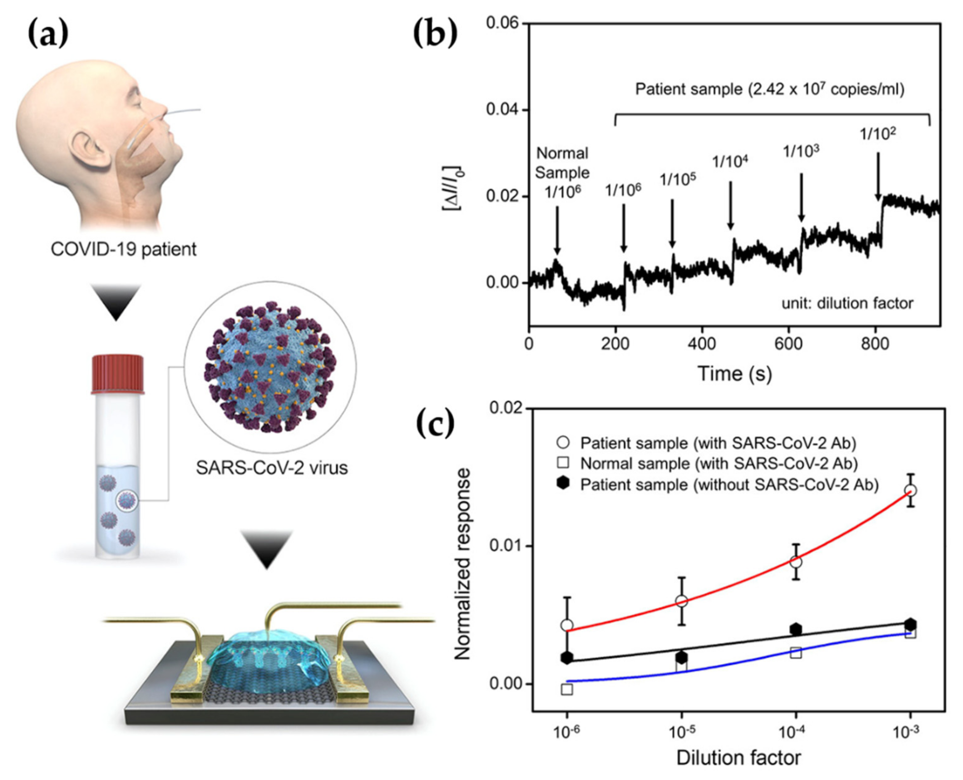
  57. Seo, G.; Lee, G.; Kim, M.J.; Baek, S.-H.H.; Choi, M.; Ku, K.B.; Lee, C.-S.S.; Jun, S.; Park, D.; Kim, H.G.; et al. Rapid detection of COVID-19 causative virus (SARS-CoV-2) in human nasopharyngeal swab specimens using field-effect transistor-based biosensor. ACS Nano 2020, 14, 5135–5142. [Google Scholar] [CrossRef] [PubMed] [Green Version]
  58. Sarkar, D.; Liu, W.; Xie, X.; Anselmo, A.C.; Mitragotri, S.; Banerjee, K. MoS2 field-effect transistor for next-generation label-free biosensors. ACS Nano 2014, 8, 3992–4003. [Google Scholar] [CrossRef]
  59. Picca, R.A.; Manoli, K.; Macchia, E.; Sarcina, L.; Di Franco, C.; Cioffi, N.; Blasi, D.; Österbacka, R.; Torricelli, F.; Scamarcio, G.; et al. Ultimately sensitive organic bioelectronic transistor sensors by materials and device structure design. Adv. Funct. Mater. 2020, 30, 1–23. [Google Scholar] [CrossRef]
  60. Kim, D.-S.; Park, J.-E.; Shin, J.-K.; Kim, P.K.; Lim, G.; Shoji, S. An extended gate FET-based biosensor integrated with a Si microfluidic channel for detection of protein complexes. Sens. Actuators B Chem. 2006, 117, 488–494. [Google Scholar] [CrossRef]
  61. Kim, J.; Rim, Y.S.; Chen, H.; Cao, H.H.; Nakatsuka, N.; Hinton, H.L.; Zhao, C.; Andrews, A.M.; Yang, Y.; Weiss, P.S. Fabrication of high-performance ultrathin In2O3 film field-effect transistors and biosensors using chemical lift-off lithography. ACS Nano 2015, 9, 4572–4582. [Google Scholar] [CrossRef] [Green Version]
  62. Parkula, V.; Berto, M.; Diacci, C.; Patrahau, B.; Di Lauro, M.; Kovtun, A.; Liscio, A.; Sensi, M.; Samorì, P.; Greco, P.; et al. Harnessing selectivity and sensitivity in electronic biosensing: A novel lab-on-chip multigate organic transistor. Anal. Chem. 2020, 92, 9330–9337. [Google Scholar] [CrossRef]
  63. Buth, F.; Donner, A.; Sachsenhauser, M.; Stutzmann, M.; Garrido, J.A. Biofunctional electrolyte-gated organic field-effect transistors. Adv. Mater. 2012, 24, 4511–4517. [Google Scholar] [CrossRef]
  64. Macchia, E.; Sarcina, L.; Picca, R.A.; Manoli, K.; Di Franco, C.; Scamarcio, G.; Torsi, L. Ultra-low HIV-1 p24 detection limits with a bioelectronic sensor. Anal. Bioanal. Chem. 2020, 412, 811–818. [Google Scholar] [CrossRef] [Green Version]
  65. Yin, P.T.; Shah, S.; Chhowalla, M.; Lee, K.B. Design, synthesis, and characterization of graphene-nanoparticle hybrid materials for bioapplications. Chem. Rev. 2015, 115, 2483–2531. [Google Scholar] [CrossRef] [PubMed] [Green Version]
  66. Meng, Z.; Stolz, R.M.; Mendecki, L.; Mirica, K.A. Electrically-transduced chemical sensors based on two-dimensional nanomaterials. Chem. Rev. 2019, 119, 478–598. [Google Scholar] [CrossRef] [PubMed]
  67. Yang, Y.; Asiri, A.M.; Tang, Z.; Du, D.; Lin, Y. Graphene based materials for biomedical applications. Mater. Today 2013, 16, 365–373. [Google Scholar] [CrossRef]
  68. Chen, Y.; Ren, R.; Pu, H.; Chang, J.; Mao, S.; Chen, J. Field-effect transistor biosensors with two-dimensional black phosphorus nanosheets. Biosens. Bioelectron. 2017, 89, 505–510. [Google Scholar] [CrossRef] [PubMed] [Green Version]
  69. Alabsi, S.S.; Ahmed, A.Y.; Dennis, J.O.; Khir, M.H.M.; Algamili, A.S. A Review of carbon nanotubes field effect-based biosensors. IEEE Access 2020, 8, 69509–69521. [Google Scholar] [CrossRef]
  70. Béraud, A.; Sauvage, M.; Bazán, C.M.; Tie, M.; Bencherif, A.; Bouilly, D. Graphene field-effect transistors as bioanalytical sensors: Design, operation and performance. Analyst 2021, 146, 403–428. [Google Scholar] [CrossRef]
  71. Fakih, I.; Mahvash, F.; Siaj, M.; Szkopek, T. Sensitive precise pH measurement with large-area graphene field-effect transistors at the quantum-capacitance limit. Phys. Rev. Appl. 2017, 8, 044022. [Google Scholar] [CrossRef]
  72. Ahmad, W.; Gong, Y.; Abbas, G.; Khan, K.; Khan, M.; Ali, G.; Shuja, A.; Tareen, A.K.; Khan, Q.; Li, D. Evolution of low-dimensional material-based field-effect transistors. Nanoscale 2021, 13, 5162–5186. [Google Scholar] [CrossRef]
  73. Bolotsky, A.; Butler, D.; Dong, C.; Gerace, K.; Glavin, N.R.; Muratore, C.; Robinson, J.A.; Ebrahimi, A. Two-dimensional materials in biosensing and healthcare: From in vitro diagnostics to optogenetics and beyond. ACS Nano 2019, 13, 9781–9810. [Google Scholar] [CrossRef] [Green Version]
  74. Wang, Y.; Xu, Y.; Hu, M.; Ling, H.; Zhu, X. MXenes: Focus on optical and electronic properties and corresponding applications. Nanophotonics 2020, 9, 1601–1620. [Google Scholar] [CrossRef]
  75. Jiang, X.; Kuklin, A.V.; Baev, A.; Ge, Y.; Ågren, H.; Zhang, H.; Prasad, P.N. Two-dimensional MXenes: From morphological to optical, electric, and magnetic properties and applications. Phys. Rep. 2020, 848, 1–58. [Google Scholar] [CrossRef]
  76. Zhang, X.; Zhao, X.; Wu, D.; Jing, Y.; Zhou, Z. High and anisotropic carrier mobility in experimentally possible Ti2CO2 (MXene) monolayers and nanoribbons. Nanoscale 2015, 7, 16020–16025. [Google Scholar] [CrossRef] [PubMed]
  77. Khan, R.; Andreescu, S. Mxenes-based bioanalytical sensors: Design, characterization, and applications. Sensors 2020, 20, 5434. [Google Scholar] [CrossRef] [PubMed]
  78. Hutagalung, S.D.; Fadhali, M.M.; Areshi, R.A.; Tan, F.D. Optical and electrical characteristics of silicon nanowires prepared by electroless etching. Nanoscale Res. Lett. 2017, 12, 425. [Google Scholar] [CrossRef] [PubMed] [Green Version]
  79. Avouris, P.; Chen, Z.; Perebeinos, V. Carbon-based electronics. Nat. Nanotechnol. 2007, 2, 605–615. [Google Scholar] [CrossRef]
  80. Lee, M.; Jeon, Y.; Sik Son, K.; Hyung Shim, J.; Kim, S. Comparative performance analysis of silicon nanowire tunnel FETs and MOSFETs on plastic substrates in flexible logic circuit applications. Phys. Status Solid 2012, 209, 1350–1358. [Google Scholar] [CrossRef]
  81. Li, X.; Wang, X.; Zhang, L.; Lee, S.; Dai, H. Chemically derived, ultrasmooth graphene nanoribbon semiconductors. Science 2008, 319, 1229–1232. [Google Scholar] [CrossRef]
  82. Li, X.; Zhu, H. Two-dimensional MoS2: Properties, preparation, and applications. J. Mater. 2015, 1, 33–44. [Google Scholar] [CrossRef] [Green Version]
  83. Li, L.; Yu, Y.; Ye, G.J.; Ge, Q.; Ou, X.; Wu, H.; Feng, D.; Chen, X.H.; Zhang, Y. Black phosphorus field-effect transistors. Nat. Nanotechnol. 2014, 9, 372–377. [Google Scholar] [CrossRef] [Green Version]
  84. Chen, X.; Bi, Q.; Sajjad, M.; Wang, X.; Ren, Y.; Zhou, X.; Xu, W.; Liu, Z. One-dimensional porous silicon nanowires with large surface area for fast charge–discharge lithium-ion batteries. Nanomaterials 2018, 8, 285. [Google Scholar] [CrossRef] [Green Version]
  85. Zhang, S.; Wang, H.; Liu, J.; Bao, C. Measuring the specific surface area of monolayer graphene oxide in water. Mater. Lett. 2020, 261, 127098. [Google Scholar] [CrossRef]
  86. Cheng, J.; Gao, L.; Li, T.; Mei, S.; Wang, C.; Wen, B.; Huang, W.; Li, C.; Zheng, G.; Wang, H.; et al. Two-dimensional black phosphorus nanomaterials: Emerging advances in electrochemical energy storage science. Nano Micro Lett. 2020, 12, 179. [Google Scholar] [CrossRef] [PubMed]
  87. Zhou, Y.; Fang, Y.; Ramasamy, R. Non-covalent functionalization of carbon nanotubes for electrochemical biosensor development. Sensors 2019, 19, 392. [Google Scholar] [CrossRef] [PubMed] [Green Version]
  88. Doucey, M.-A.; Carrara, S. Nanowire sensors in cancer. Trends Biotechnol. 2019, 37, 86–99. [Google Scholar] [CrossRef] [Green Version]
  89. Lee, J.; Dak, P.; Lee, Y.; Park, H.; Choi, W.; Alam, M.A.; Kim, S. Two-dimensional layered MoS2 biosensors enable highly sensitive detection of biomolecules. Sci. Rep. 2015, 4, 7352. [Google Scholar] [CrossRef] [Green Version]
  90. Kukkar, M.; Tuteja, S.K.; Sharma, A.L.; Kumar, V.; Paul, A.K.; Kim, K.-H.; Sabherwal, P.; Deep, A. A new electrolytic synthesis method for few-layered MoS2 nanosheets and their robust biointerfacing with reduced antibodies. ACS Appl. Mater. Interfaces 2016, 8, 16555–16563. [Google Scholar] [CrossRef]
  91. Xu, B.; Zhi, C.; Shi, P. Latest advances in MXene biosensors. J. Phys. Mater. 2020, 3, 031001. [Google Scholar] [CrossRef]
  92. Patolsky, F.; Zheng, G.; Lieber, C.M. Fabrication of silicon nanowire devices for ultrasensitive, label-free, real-time detection of biological and chemical species. Nat. Protoc. 2006, 1, 1711–1724. [Google Scholar] [CrossRef] [PubMed]
  93. Agarwal, V.; Chatterjee, K. Recent advances in the field of transition metal dichalcogenides for biomedical applications. Nanoscale 2018, 10, 16365–16397. [Google Scholar] [CrossRef]
  94. Naguib, M.; Mochalin, V.N.; Barsoum, M.W.; Gogotsi, Y. 25th Anniversary article: MXenes: A new family of two-dimensional materials. Adv. Mater. 2014, 26, 992–1005. [Google Scholar] [CrossRef] [PubMed]
  95. de Freitas Martins, E.; Troiano Feliciano, G.; Hendrik Scheicher, R.; Reily Rocha, A. Simulating DNA Chip Design Using All-Electronic Graphene-Based Substrates. Molecules 2019, 24, 951. [Google Scholar] [CrossRef] [PubMed] [Green Version]
  96. Tsang, D.K.H.; Lieberthal, T.J.; Watts, C.; Dunlop, I.E.; Ramadan, S.; del Rio Hernandez, A.E.; Klein, N. Chemically functionalised graphene FET biosensor for the label-free sensing of exosomes. Sci. Rep. 2019, 9, 2–11. [Google Scholar] [CrossRef] [Green Version]
  97. Huang, W.; Diallo, A.K.; Dailey, J.L.; Besar, K.; Katz, H.E. Electrochemical processes and mechanistic aspects of field-effect sensors for biomolecules. J. Mater. Chem. C 2015, 3, 6445–6470. [Google Scholar] [CrossRef]
  98. Iijima, S. Helical microtubules of graphitic carbon. Nature 1991, 354, 56–58. [Google Scholar] [CrossRef]
  99. Sedki, M.; Shen, Y.; Mulchandani, A. Nano-FET-enabled biosensors: Materials perspective and recent advances in North America. Biosens. Bioelectron. 2021, 176, 112941. [Google Scholar] [CrossRef] [PubMed]
  100. Martel, R.; Schmidt, T.; Shea, H.R.; Hertel, T.; Avouris, P. Single- and multi-wall carbon nanotube field-effect transistors. Appl. Phys. Lett. 1998, 73, 2447–2449. [Google Scholar] [CrossRef] [Green Version]
  101. Chang, Y.W.; Oh, J.S.; Yoo, S.H.; Choi, H.H.; Yoo, K.-H. Electrically refreshable carbon-nanotube-based gas sensors. Nanotechnology 2007, 18, 435504. [Google Scholar] [CrossRef]
  102. Melzer, K.; Bhatt, V.D.; Jaworska, E.; Mittermeier, R.; Maksymiuk, K.; Michalska, A.; Lugli, P. Enzyme assays using sensor arrays based on ion-selective carbon nanotube field-effect transistors. Biosens. Bioelectron. 2016, 84, 7–14. [Google Scholar] [CrossRef]
  103. Kuang, Z.; Kim, S.N.; Crookes-Goodson, W.J.; Farmer, B.L.; Naik, R.R. Biomimetic chemosensor: Designing peptide recognition elements for surface functionalization of carbon nanotube field-effect transistors. ACS Nano 2010, 4, 452–458. [Google Scholar] [CrossRef]
  104. Xuan, C.T.; Thuy, N.T.; Luyen, T.T.; Huyen, T.T.T.; Tuan, M.A. Carbon Nanotube Field-Effect Transistor for DNA Sensing. J. Electron. Mater. 2017, 46, 3507–3511. [Google Scholar] [CrossRef]
  105. Ko, J.W.; Woo, J.-M.; Jinhong, A.; Cheon, J.H.; Lim, J.H.; Kim, S.H.; Chun, H.; Kim, E.; Park, Y.J. Multi-Order dynamic range dna sensor using a gold decorated swcnt random network. ACS Nano 2011, 5, 4365–4372. [Google Scholar] [CrossRef]
  106. Shao, W.; Shurin, M.R.; Wheeler, S.E.; He, X.; Star, A. rapid detection of SARS-CoV-2 antigens using high-purity semiconducting single-walled carbon nanotube-based field-effect transistors. ACS Appl. Mater. Interfaces 2021. [Google Scholar] [CrossRef]
  107. Münzer, A.M.; Seo, W.; Morgan, G.J.; Michael, Z.P.; Zhao, Y.; Melzer, K.; Scarpa, G.; Star, A. Sensing reversible protein-ligand interactions with single-walled carbon nanotube field-effect transistors. J. Phys. Chem. C 2014, 118, 17193–17199. [Google Scholar] [CrossRef] [PubMed] [Green Version]
  108. Lapedus, M. Chasing after Carbon Nanotube FETs. Available online: https://semiengineering.com/chasing-after-carbon-nanotube-fets/ (accessed on 25 March 2021).
  109. Fischer, M.J.E. Amine coupling through EDC/NHS: A practical approach. In Surface Plasmon Resonance: Methods and Protocols; Mol, N.J., Fischer, M.J.E., Eds.; Humana Press: Totowa, NJ, USA, 2010; pp. 55–73. ISBN 978-1-60761-670-2. [Google Scholar]
  110. Amoretti, M.; Amsler, C.; Bonomi, G.; Bouchta, A.; Bowe, P.; Carraro, C.; Cesar, C.L.; Charlton, M.; Collier, M.J.T.; Doser, M.; et al. Production and detection of cold antihydrogen atoms. Nature 2002, 419, 456–459. [Google Scholar] [CrossRef]
  111. Alim, S.; Vejayan, J.; Yusoff, M.M.; Kafi, A.K.M. Recent uses of carbon nanotubes & gold nanoparticles in electrochemistry with application in biosensing: A review. Biosens. Bioelectron. 2018, 121, 125–136. [Google Scholar] [CrossRef] [PubMed]
  112. Sadighbayan, D.; Hasanzadeh, M.; Ghafar-Zadeh, E. Biosensing based on field-effect transistors (FET): Recent progress and challenges. TrAC Trends Anal. Chem. 2020, 133, 116067. [Google Scholar] [CrossRef] [PubMed]
  113. Mao, S.; Lu, G.; Yu, K.; Chen, J. Specific biosensing using carbon nanotubes functionalized with gold nanoparticle–antibody conjugates. Carbon N. Y. 2010, 48, 479–486. [Google Scholar] [CrossRef]
  114. Kim, J.P.; Lee, B.Y.; Lee, J.; Hong, S.; Sim, S.J. Enhancement of sensitivity and specificity by surface modification of carbon nanotubes in diagnosis of prostate cancer based on carbon nanotube field effect transistors. Biosens. Bioelectron. 2009, 24, 3372–3378. [Google Scholar] [CrossRef]
  115. Michael, Z.P.; Shao, W.; Sorescu, D.C.; Euler, R.W.; Burkert, S.C.; Star, A. Probing biomolecular interactions with gold nanoparticle-decorated single-walled carbon nanotubes. J. Phys. Chem. C 2017, 121, 20813–20820. [Google Scholar] [CrossRef]
  116. Ding, M.; Tang, Y.; Star, A. Understanding interfaces in metal–graphitic hybrid nanostructures. J. Phys. Chem. Lett. 2013, 4, 147–160. [Google Scholar] [CrossRef]
  117. Schmidt, V.; Wittemann, J.V.; Senz, S.; Gösele, U. Silicon nanowires: A review on aspects of their growth and their electrical properties. Adv. Mater. 2009, 21, 2681–2702. [Google Scholar] [CrossRef]
  118. Tran, D.P.; Wolfrum, B.; Stockmann, R.; Pai, J.-H.; Pourhassan-Moghaddam, M.; Offenhäusser, A.; Thierry, B. Complementary metal oxide semiconductor compatible silicon nanowires-on-a-chip: Fabrication and preclinical validation for the detection of a cancer prognostic protein marker in serum. Anal. Chem. 2015, 87, 1662–1668. [Google Scholar] [CrossRef]
  119. Gonchar, K.A.; Agafilushkina, S.N.; Moiseev, D.V.; Bozhev, I.V.; Manykin, A.A.; Kropotkina, E.A.; Gambaryan, A.S.; Osminkina, L.A. H1N1 influenza virus interaction with a porous layer of silicon nanowires. Mater. Res. Express 2020, 7, 035002. [Google Scholar] [CrossRef]
  120. Gao, A.; Yang, X.; Tong, J.; Zhou, L.; Wang, Y.; Zhao, J.; Mao, H.; Li, T. Multiplexed detection of lung cancer biomarkers in patients serum with CMOS-compatible silicon nanowire arrays. Biosens. Bioelectron. 2017, 91, 482–488. [Google Scholar] [CrossRef] [PubMed]
  121. Chartuprayoon, N.; Zhang, M.; Bosze, W.; Choa, Y.H.; Myung, N.V. One-dimensional nanostructures based bio-detection. Biosens. Bioelectron. 2015, 63, 432–443. [Google Scholar] [CrossRef] [PubMed]
  122. Mu, L.; Chang, Y.; Sawtelle, S.D.; Wipf, M.; Duan, X.; Reed, M.A. Silicon nanowire field-effect transistors—A versatile class of potentiometric nanobiosensors. IEEE Access 2015, 3, 287–302. [Google Scholar] [CrossRef]
  123. Chen, K.I.; Li, B.R.; Chen, Y.T. Silicon nanowire field-effect transistor-based biosensors for biomedical diagnosis and cellular recording investigation. Nano Today 2011, 6, 131–154. [Google Scholar] [CrossRef]
  124. Chang, S.-M.; Palanisamy, S.; Wu, T.-H.; Chen, C.-Y.; Cheng, K.-H.; Lee, C.-Y.; Yuan, S.-S.F.; Wang, Y.-M. Utilization of silicon nanowire field-effect transistors for the detection of a cardiac biomarker, cardiac troponin I and their applications involving animal models. Sci. Rep. 2020, 10, 22027. [Google Scholar] [CrossRef]
  125. Smith, R.; Geary, S.M.; Salem, A.K. Silicon nanowires and their impact on cancer detection and monitoring. ACS Appl. Nano Mater. 2020. [Google Scholar] [CrossRef]
  126. Tran, D.P.; Winter, M.A.; Wolfrum, B.; Stockmann, R.; Yang, C.-T.; Pourhassan-Moghaddam, M.; Offenhäusser, A.; Thierry, B. Toward intraoperative detection of disseminated tumor cells in lymph nodes with silicon nanowire field-effect transistors. ACS Nano 2016, 10, 2357–2364. [Google Scholar] [CrossRef] [Green Version]
  127. Li, J.; Zhang, Y.; To, S.; You, L.; Sun, Y. Effect of nanowire number, diameter, and doping density on nano-fet biosensor sensitivity. ACS Nano 2011, 5, 6661–6668. [Google Scholar] [CrossRef] [PubMed]
  128. Nair, P.R.; Alam, M.A. Design considerations of silicon nanowire biosensors. IEEE Trans. Electron Devices 2007, 54, 3400–3408. [Google Scholar] [CrossRef]
  129. Fathil, M.F.M.; Arshad, M.K.M.; Nuzaihan, M.N.M.; Gopinath, S.C.B.; Ruslinda, A.R.; Hashim, U. The ZnO-FET biosensor for cardiac troponin I. IOP Conf. Ser. Mater. Sci. Eng. 2018, 318. [Google Scholar] [CrossRef]
  130. Chakraborty, B.; Ghosh, S.; Das, N.; RoyChaudhuri, C. Liquid gated ZnO nanorod FET sensor for ultrasensitive detection of Hepatitis B surface antigen with vertical electrode configuration. Biosens. Bioelectron. 2018, 122, 58–67. [Google Scholar] [CrossRef] [PubMed]
  131. Ditshego, N.M.J. Zno nanowire field effect transistor for biosensing: A review. J. Nano Res. 2019, 60, 94–112. [Google Scholar] [CrossRef] [Green Version]
  132. Joyce, H.J.; Docherty, C.J.; Gao, Q.; Tan, H.H.; Jagadish, C.; Lloyd-Hughes, J.; Herz, L.M.; Johnston, M.B. Electronic properties of GaAs, InAs and InP nanowires studied by terahertz spectroscopy. Nanotechnology 2013, 24, 214006. [Google Scholar] [CrossRef]
  133. Ahn, M.S.; Ahmad, R.; Bhat, K.S.; Yoo, J.Y.; Mahmoudi, T.; Hahn, Y.B. Fabrication of a solution-gated transistor based on valinomycin modified iron oxide nanoparticles decorated zinc oxide nanorods for potassium detection. J. Colloid Interface Sci. 2018, 518, 277–283. [Google Scholar] [CrossRef]
  134. Novoselov, K.S. Electric Field Effect in Atomically Thin Carbon Films. Science 2004, 306, 666–669. [Google Scholar] [CrossRef] [Green Version]
  135. Schedin, F.; Geim, A.K.; Morozov, S.V.; Hill, E.W.; Blake, P.; Katsnelson, M.I.; Novoselov, K.S. Detection of individual gas molecules adsorbed on graphene. Nat. Mater. 2007, 6, 652–655. [Google Scholar] [CrossRef] [PubMed]
  136. Ang, P.K.; Chen, W.; Wee, A.T.S.; Loh, K.P. Solution-Gated Epitaxial Graphene as pH Sensor. J. Am. Chem. Soc. 2008, 130, 14392–14393. [Google Scholar] [CrossRef]
  137. Mohanty, N.; Berry, V. Graphene-based single-bacterium resolution biodevice and DNA transistor: Interfacing graphene derivatives with nanoscale and microscale biocomponents. Nano Lett. 2008, 8, 4469–4476. [Google Scholar] [CrossRef]
  138. Mao, S.; Lu, G.; Yu, K.; Bo, Z.; Chen, J. Specific Protein Detection Using Thermally Reduced Graphene Oxide Sheet Decorated with Gold Nanoparticle-Antibody Conjugates. Adv. Mater. 2010, 22, 3521–3526. [Google Scholar] [CrossRef]
  139. Ohno, Y.; Maehashi, K.; Matsumoto, K. Label-free biosensors based on aptamer-modified graphene field-effect transistors. J. Am. Chem. Soc. 2010, 132, 18012–18013. [Google Scholar] [CrossRef] [PubMed]
  140. Zhu, J.; Niu, F.; Zhu, C.; Yang, J.; Xi, N. Graphene-based FET detector for E. coli K12 real-time monitoring and its theoretical analysis. J. Sens. 2016, 2016. [Google Scholar] [CrossRef]
  141. Zhou, L.; Mao, H.; Wu, C.; Tang, L.; Wu, Z.; Sun, H.; Zhang, H.; Zhou, H.; Jia, C.; Jin, Q.; et al. Label-free graphene biosensor targeting cancer molecules based on non-covalent modification. Biosens. Bioelectron. 2017, 87, 701–707. [Google Scholar] [CrossRef] [Green Version]
  142. Islam, S.; Shukla, S.; Bajpai, V.K.; Han, Y.K.; Huh, Y.S.; Kumar, A.; Ghosh, A.; Gandhi, S. A smart nanosensor for the detection of human immunodeficiency virus and associated cardiovascular and arthritis diseases using functionalized graphene-based transistors. Biosens. Bioelectron. 2019, 126, 792–799. [Google Scholar] [CrossRef]
  143. Kanai, Y.; Ohmuro-Matsuyama, Y.; Tanioku, M.; Ushiba, S.; Ono, T.; Inoue, K.; Kitaguchi, T.; Kimura, M.; Ueda, H.; Matsumoto, K. Graphene field effect transistor-based immunosensor for ultrasensitive noncompetitive detection of small antigens. ACS Sens. 2020, 5, 24–28. [Google Scholar] [CrossRef]
  144. Perez, A.; Amorim, R.G.; Villegas, C.E.P.; Rocha, A.R. Nanogap-based all-electronic DNA sequencing devices using MoS2 monolayers. Phys. Chem. Chem. Phys. 2020, 22, 27053–27059. [Google Scholar] [CrossRef] [PubMed]
  145. Mak, K.F.; Lee, C.; Hone, J.; Shan, J.; Heinz, T.F. Atomically thin MoS2: A new direct-gap semiconductor. Phys. Rev. Lett. 2010, 105, 136805. [Google Scholar] [CrossRef] [Green Version]
  146. Wang, L.; Wang, Y.; Wong, J.I.; Palacios, T.; Kong, J.; Yang, H.Y. Functionalized MoS2 nanosheet-based field-effect biosensor for label-free sensitive detection of cancer marker proteins in solution. Small 2014, 10, 1101–1105. [Google Scholar] [CrossRef]
  147. Nam, H.; Oh, B.-R.; Chen, P.; Chen, M.; Wi, S.; Wan, W.; Kurabayashi, K.; Liang, X. Multiple MoS2 Transistors for Sensing Molecule Interaction Kinetics. Sci. Rep. 2015, 5, 10546. [Google Scholar] [CrossRef] [Green Version]
  148. Nam, H.; Oh, B.-R.; Chen, P.; Yoon, J.S.; Wi, S.; Chen, M.; Kurabayashi, K.; Liang, X. Two different device physics principles for operating MoS2 transistor biosensors with femtomolar-level detection limits. Appl. Phys. Lett. 2015, 107, 012105. [Google Scholar] [CrossRef]
  149. Ryu, B.; Nam, H.; Oh, B.-R.; Song, Y.; Chen, P.; Park, Y.; Wan, W.; Kurabayashi, K.; Liang, X. Cyclewise operation of printed MoS2 transistor biosensors for rapid biomolecule quantification at femtomolar levels. ACS Sens. 2017, 2, 274–281. [Google Scholar] [CrossRef] [PubMed]
  150. Zhang, P.; Yang, S.; Pineda-Gómez, R.; Ibarlucea, B.; Ma, J.; Lohe, M.R.; Akbar, T.F.; Baraban, L.; Cuniberti, G.; Feng, X. Electrochemically exfoliated high-quality 2H-MoS2 for multiflake thin film flexible biosensors. Small 2019, 1901265. [Google Scholar] [CrossRef] [PubMed]
  151. Kim, J.; Sando, S.; Cui, T. Biosensor Based on Layer by Layer Deposited Phosphorene Nanoparticles for Liver Cancer Detection. In Proceedings of the Volume 2: Advanced Manufacturing; American Society of Mechanical Engineers, Tampa, FL, USA, 3–9 November 2017. [Google Scholar]
  152. Naguib, M.; Kurtoglu, M.; Presser, V.; Lu, J.; Niu, J.; Heon, M.; Hultman, L.; Gogotsi, Y.; Barsoum, M.W. Two-dimensional nanocrystals produced by exfoliation of Ti3AlC2. Adv. Mater. 2011, 23, 4248–4253. [Google Scholar] [CrossRef] [Green Version]
  153. Li, Y.; Peng, Z.; Holl, N.J.; Hassan, M.R.; Pappas, J.M.; Wei, C.; Izadi, O.H.; Wang, Y.; Dong, X.; Wang, C.; et al. MXene–graphene field-effect transistor sensing of influenza virus and SARS-CoV-2. ACS Omega 2021, 6, 6643–6653. [Google Scholar] [CrossRef]
  154. Rafat, N.; Satoh, P.; Calabrese Barton, S.; Worden, R.M. Integrated experimental and theoretical studies on an electrochemical immunosensor. Biosensors 2020, 10, 144. [Google Scholar] [CrossRef]
  155. De Freitas Martins, E.; Amorim, R.G.; Feliciano, G.T.; Scheicher, R.H.; Rocha, A.R. The role of water on the electronic transport in graphene nanogap devices designed for DNA sequencing. Carbon N. Y. 2020, 158, 314–319. [Google Scholar] [CrossRef]
  156. Kogikoski, S.; Sousa, C.P.; Liberato, M.S.; Andrade-Filho, T.; Prieto, T.; Ferreira, F.F.; Rocha, A.R.; Guha, S.; Alves, W.A. Multifunctional biosensors based on peptide–polyelectrolyte conjugates. Phys. Chem. Chem. Phys. 2016, 18, 3223–3233. [Google Scholar] [CrossRef] [PubMed]
  157. Lowe, B.M.; Skylaris, C.K.; Green, N.G.; Shibuta, Y.; Sakata, T. Molecular dynamics simulation of potentiometric sensor response: The effect of biomolecules, surface morphology and surface charge. Nanoscale 2018, 10, 8650–8666. [Google Scholar] [CrossRef] [PubMed] [Green Version]
  158. Mirzaii Babolghani, F.; Mohammadi-Manesh, E. Simulation and experimental study of FET biosensor to detect polycyclic aromatic hydrocarbons. Appl. Surf. Sci. 2019, 488, 662–670. [Google Scholar] [CrossRef]
  159. Stroud, A.; Leuty, G.; Muratore, C.; Derosa, P.A.; Berry, R. Molecular dynamics simulation of the interaction of HLL peptide and 2D materials with individual residue resolution. Comput. Mater. Sci. 2019, 169, 109112. [Google Scholar] [CrossRef]
  160. Badhe, Y.; Gupta, R.; Rai, B. In silico design of peptides with binding to the receptor binding domain (RBD) of the SARS-CoV-2 and their utility in bio-sensor development for SARS-CoV-2 detection. RSC Adv. 2021, 11, 3816–3826. [Google Scholar] [CrossRef]
  161. de Souza, F.A.L.; Amorim, R.G.; Prasongkit, J.; Scopel, W.L.; Scheicher, R.H.; Rocha, A.R. Topological line defects in graphene for applications in gas sensing. Carbon N. Y. 2018, 129, 803–808. [Google Scholar] [CrossRef] [Green Version]
  162. Rocha, A.R.; García-suárez, V.M.; Bailey, S.W.; Lambert, C.J.; Ferrer, J.; Sanvito, S. Towards molecular spintronics. Nat. Mater. 2005, 4, 335–339. [Google Scholar] [CrossRef]
  163. Li, J.H.; Wu, J.; Yu, Y.X. DFT exploration of sensor performances of two-dimensional WO3 to ten small gases in terms of work function and band gap changes and I-V responses. Appl. Surf. Sci. 2021, 546, 149104. [Google Scholar] [CrossRef]
  164. Prasongkit, J.; de Freitas Martins, E.; de Souza, F.A.L.; Scopel, W.L.; Amorim, R.G.; Amornkitbamrung, V.; Rocha, A.R.; Scheicher, R.H. Topological Line Defects Around Graphene Nanopores for DNA Sequencing. J. Phys. Chem. C 2018, 122, 7094–7099. [Google Scholar] [CrossRef] [Green Version]
  165. Lee, J.H.; Choi, Y.K.; Kim, H.J.; Scheicher, R.H.; Cho, J.H. Physisorption of DNA nucleobases on h-BN and graphene: VdW-corrected DFT calculations. J. Phys. Chem. C 2013, 117, 13435–13441. [Google Scholar] [CrossRef] [Green Version]
  166. Civitarese, T.; Zollo, G. Triggering amino acid detection by atomistic resolved tunneling current signals in graphene nanoribbon devices for peptide sequencing. ACS Appl. Nano Mater. 2021, 4, 363–371. [Google Scholar] [CrossRef]
  167. Feliciano, G.T.; Sanz-Navarro, C.; Coutinho-Neto, M.D.; Ordejón, P.; Scheicher, R.H.; Rocha, A.R. Capacitive DNA detection driven by electronic charge fluctuations in a graphene nanopore. Phys. Rev. Appl. 2015, 3, 1–7. [Google Scholar] [CrossRef]
Figure 1. Schematic representation of (a) solution-gated field-effect transistor (SGFET), (b) ion-sensitive field-effect transistor (ISFET), and (c) field-effect transistor-based biosensor (BioFET) with their equivalent circuits, respectively. (d) The characteristic curves of the SGFET, output (i) IDS vs. VDS and transfer (ii) IDS vs. VGS. Adapted from [52] with permission from Elsevier.
Chemosensors 09 00162 g001
Figure 2. (a) Sketch of a solution-gated field-effect transistor (SGFET) immunosensor platform. A source, a drain, and gate electrodes form the basics of a FET device. The biorecognition event occurs when the antigens (light green squares) bind to its specific antibody (orange Y), immobilized at the surface of the semiconductor. Examples of immunosensors based field-effect transistor (FET). (b) Indium phosphide (InP) nanowire (NW) FET device and scanning electron microscopy (SEM) image showing the InP NW between source and drain electrode. Adapted from [55] with permission from ACS. (c) Carbon nanotubes (CNTs) FET device (i) atomic force microscopy (AFM) image showing an individual single-walled carbon nanotube (SWCNT) between source and drain electrodes and (ii) an SEM image of an array of SWCNTs. Adapted from [56] with permission from Wiley. Optical image of (d) graphene and (e) molybdenum disulfide (MoS2) FET devices. Adapted from [57] and [58], respectively, with permission from ACS.
Chemosensors 09 00162 g002
Figure 3. Field-effect transistor based on single-walled carbon nanotube (SWCNT) decorated with Au nanoparticles (NPs) for the detection of GSH and GSSG. (a) Transfer characteristics (IDS vs. VGS) for the SWCNTs before and after the electrodeposition of Au NPs and (b) for the detection of reduced glutathione (GSH) (i) and oxidized glutathione (GSSG) (ii). (c) Results of density functional theory calculations for two representative adsorption configurations of GSSG and GSH on the hybrid Au80-(14,0) SWCNT system. Panels (i) and (iv) represent the charge difference maps for GSSG and GSH at the interface between the molecules and the Au nanocluster. Panels (ii) and (v) show the charge difference maps at the interface between the Au nanocluster and the SWCNT. Panels (iii) and (vi) show the partial charge density (isovalue of 0.01 e3) corresponding to the electronic bands within a 0.2 eV interval above the Fermi level. (d) Total density of states and the local density of states of SWCNT, Au cluster, and the individual GSSG (i) or GSH (ii) molecules. Adapted from [115] with permission from ACS.
Chemosensors 09 00162 g003
Figure 4. Silicon-nanowire-field-effect-transistor-based (SiNW-FET) immunosensors. (a) Schematic representation of the conductance change in a SiNW-FET-based immunosensor as a function of the target molecule charge. Adapted from [123] with permission from Elsevier. (b) Schematic representation of the chemical process involved in the modification of silicon nanowire (SiNW) surface: (i) Binding of 3-aminopropyl triethoxysilane (APTES) to SiNW, (ii) addition of bifunctional linker glutaraldehyde and (iii) antibody attachment, and (iv) antigen detection. Adapted from [124] with permission from Springer Nature. (c) Schematic representation of how the diameter of a wire affects the change in its conductance: (i) for thick wires, the surface-to-volume ratio is relatively small. When the wire surface is approached by charged particles (red ball), only the conductance near the wire surface is affected. There is still a large interior area of the wire that might not be influenced (gray circle). (ii) As the wire diameter is reduced to the nanoscale, the surface-to-volume ratio drastically increases. Therefore, the same external electrical field (pink area) caused by the charged particles (red ball) could influence most of the inner region of the nanowire, thus drastically changing its conductance. Adapted from [123] with permission from Elsevier.
Chemosensors 09 00162 g004
Figure 5. (a) Schematic illustration of the zinc-oxide-nanorod-field-effect-transistor-based (ZnO-NR-FET) immunosensors with lateral (i) and vertical (ii) electrode configuration, respectively. (b) Variation of sensitivity with different antigen concentrations for 1 MHz frequency for vertical and horizontal electrode configuration. (c) Resistance model for vertical (i) and lateral (ii) electrode configuration. Adapted from [130] with permission from Elsevier.
Chemosensors 09 00162 g005
Figure 6. Graphene field-effect transistor (GFET) biosensor for the detection of the severe acute respiratory syndrome coronavirus 2 (SARS-CoV-2) in human nasopharyngeal swab specimens. (a) Schematic of the collection of samples and graphene field-effect transistor. (b) Real-time response of the GFET biosensor for various dilutions of patient samples. (c) Response dependence curve for the dilution factor of samples. Adapted from [57] with permission from ACS Publications.
Chemosensors 09 00162 g006
Figure 7. MoS2 flexible field-effect transistor biosensor for the detection of the Ebola virus. (a) Schematic of the biosensor with antibodies anchored to the substrate and antigens recognized by the antibodies. (b) Optical images of the device fabrication and atomic force microscopy image of the MoS2 nanosheet. (c) Output characteristic curves (IDS vs. VDS) for the bending tests, showing no degradation of the IDS current. (d) Calibration curves of the device for de detection of the VP 40 with (in black dots) and without (in blue dots) the presence of the VP40 antibodies and in the presence of the interferent staphylococcal enterotoxin B (SEB) (in red dots). Adapted from [150] with permission from Wiley-VCH.
Chemosensors 09 00162 g007
Table 1. Main properties and features of the most used LMDs in FET-based immunosensors.
1D2D
LDMSingle-Walled Carbon NanotubesSilicon NanowireGrapheneTransition Metal DichalcogenidesBlack PhosphorusMXenes
Chemosensors 09 00162 i001 Chemosensors 09 00162 i002 Chemosensors 09 00162 i003 Chemosensors 09 00162 i004 Chemosensors 09 00162 i005 Chemosensors 09 00162 i006
Bandgap (eV)0.6−1.8 [73]1.1 [73]0 [73]0−3.4 [73]1.59 [73]0−1.82 [74,75]
Bandgap Tunability (eV)−0.3 [73]3 [73]0.25 [73]±1 [73]0.1 [73]1.25−1.80 [75]
Carrier Mobility (cm2 V−1 s−1)105 [73]400 [73]105 [73]1−102 [73]103 [73]7.41 × 10⁴ (Ti2CO2) [76]
Conductivity (S/cm)102−106 [77]2.95 × 10⁻² [78]6300 [66]10−4 (MoS2) [77]N/A2410 (Ti3C2) [77]
ION/IOFF ratio104 [79]106 [80]107 [81]1 × 10⁸ (MoS2) [82]105 [83]N/A
Surface Area (m2 g−1)600 [77]323.47 (Porous) [84]2630 [85]8.6 (MoS2) [77]2630 [86]93.6 (Ti3C2) [77]
Active Sitessp2 orbital of carbon (large π system), defects [66]Silanol (Si-OH) groups on the surface of the native oxide layer [66]sp2 orbital of carbon (large π system), defects [66]p orbital of chalcogenide atoms, defects [66]pZ orbital of P atom [66]O, OH, and F on the surface [66]
Resulting interactionsπ−π interaction, Van der Waals, charge transfer, covalent bond [66]Covalent bond [66]π−π interaction, Van der Waals, charge transfer, covalent bond [66]Charge transfer [66]Charge transfer [66]van der Waals, H-bond, charge transfer [66]
Functionalization strategies commonly used to immobilize antibodies on the surfaceNon-covalent functionalization by π−π interaction via PBASE; Covalent functionalization by promoting carboxyl groups on the surface followed by EDC-NHS crosslinker [87]Covalent attachment of antibodies to the NW surface through silane derivatives, i.e., APTES [88]Non-covalent functionalization by π−π interaction via PBASE; Covalent functionalization by promotion carboxyl groups on the surface followed by EDC-NHS crosslinker [87]Physical adsorption [89]; Disulfide linkages between the MoS2 nanosheets and the chemically reduced antibodies with exposed sulfhydryl (−SH) groups [90]Covalent functionalization of the protective oxide layer with silane derivatives, i.e., APTES [68]Soy phospholipid, PEGylation, photo-grafting, photopolymerization, APTES [91]
Surface propertiesHigh chemical stability, hydrophobic [56]Low chemical stability [92]High chemical stability, hydrophobic [25]Hydrophobic [93]Poor chemical stability [25]Hydrophilic [94]
APTES: (3-aminopropyl)triethoxysilane; EDC-NHS: 1-ethyl-3-(3-dimethylaminopropyl)carbodiimide—N-hydroxysuccinimide; N/A: not available; PBASE: 1-pyrenebutanoic acid succinimidyl ester; PEG: polyethylene glycol polymer.
Publisher’s Note: MDPI stays neutral with regard to jurisdictional claims in published maps and institutional affiliations.

