Capacitance Properties in Ba0.3Sr0.7Zr0.18Ti0.82O3 Thin Films on Silicon Substrate for Thin Film Capacitor Applications


College of Material Science and Engineering, Sichuan University, Chengdu 610064, China
*
Author to whom correspondence should be addressed.
Crystals 2020, 10(4), 318; https://doi.org/10.3390/cryst10040318
Submission received: 30 March 2020
/
Revised: 13 April 2020
/
Accepted: 17 April 2020
/
Published: 19 April 2020
(This article belongs to the Special Issue Synthesis and Characterization of Ferroelectrics)
Abstract
:Crystalline Ba0.3Sr0.7Zr0.18Ti0.82O3 (BSZT) thin film was grown on Pt(111)/Ti/SiO2/Si substrate using radio frequency (RF) magnetron sputtering. Based on our best knowledge, there are few reports in the literature to prepare the perovskite BSZT thin films, especially using the RF magnetron sputtering method. The microstructure of the thin films was characterized using X-ray diffraction (XRD) and scanning electron microscopy (SEM), and capacitance properties, such as capacitance density, leakage behavior, and the temperature dependence of capacitance were investigated experimentally. The prepared perovskite BSZT film showed a low leakage current density of 7.65 × 10⁻⁷ A/cm2 at 60 V, and large breakdown strength of 4 MV/cm. In addition, the prepared BSZT thin film capacitor not only exhibits an almost linear and acceptable change (ΔC/C ~13.6%) of capacitance from room temperature to 180 °C but also a large capacitance density of 1.7 nF/mm2 at 100 kHz, which show great potential for coupling and decoupling applications.
1. Introduction
Recently, the increasing demand for high-density and highly integrated electronic passive components in the microelectronics industry, has greatly accelerated research on thin film capacitors with high capacitance density (capacitance per unit area) and advanced functional dielectric films with high dielectric constant and appropriate dielectric strength [1,2,3]. Except for high capacitance density and appropriate electric breakdown strength, temperature stability is another very important parameter for dielectric capacitor applications [4]. Many international electronic industries alliances, like the now-defunct Electronic Industries Alliance (EIA) and European Committee for Electrotechnical Standardization (CENELEC), have clear demands of different temperature stability for various capacitor applications [5]; for instance, ΔC/C over the temperature range in X7R ceramics capacitor is lower than −15% to +15%. According to these standards, the ferroelectric materials which exhibit paraelectric behavior over the working temperature range, can not only have a bigger dielectric constant than the linear dielectrics, but also can satisfy some EIA Class I or EIA Class II ceramics capacitors with a high requirement of temperature stability, like high-frequency capacitors, and coupling and decoupling applications.
As one of the most studied perovskite material systems, SrTiO3 (STO) thin films have been widely used in these applications due to its high dielectric constant (~120), low dielectric loss, and low curie temperature (~250 °C) [6,7,8,9,10,11]. Compared with STO films, the Ba1−xSrxTiO3 (BST) thin films have a higher dielectric constant, which has currently become very attractive for higher integration of thin film capacitors. However, electronic hopping between Ti4+ and Ti3+ ions makes the BST thin films have a low electric breakdown strength (hardly exceeding 0.8 MV/cm) [12,13]. For this reason, BaxSr1−xZryTi1−yO3 (BSZT) ceramics are thus fabricated by the substitution of Zr4+ for Ti4+ in BST ceramics [14]. As Zr4+ is chemically more stable than Ti4+ and has a larger ionic size to expand the perovskite lattice, the substitution of Ti with Zr can improve the chemical and temperature stability, and reduce the dielectric loss [15,16]. Therefore, the BSZT thin films could be a promising dielectric thin film as an alternative to the BST or STO thin films for the high-frequency capacitors, coupling and decoupling capacitors. Thus far, the perovskite BSZT thin films are prepared by using pulse laser deposition (PLD) and Sol-Gel processing [13,15,16,17,18,19]. Radio frequency (RF) magnetron sputtering method is widely used in the preparation of advanced functional thin films; it is especially flexible in preparing high-quality oxide thin films with a large area. Based on our best knowledge, there are few reports in the literature to prepare the perovskite BSZT thin films [13,15,16,17,18,19], especially using the RF magnetron sputtering method.
In this work, the perovskite Ba0.3Sr0.7Zr0.18Ti0.82O3 thin films were prepared on Pt (111)/SiO2/Si substrates by using RF magnetron sputtering technology. According to our previous results, the Curie temperature (Tc) of Ba0.3Sr0.7Zr0.18Ti0.82O3 compounds is about −102 °C, thus the Ba0.3Sr0.7Zr0.18Ti0.82O3 thin films exhibit para-electric behavior above that temperature. Its capacitance properties were systematically characterized as a function of frequency, voltage, and temperature. In addition, its dielectric performance was compared with other reported dielectric thin-films.
2. Materials and Methods
The radio frequency (RF) magnetron sputtering method was used to deposit BSZT thin films on Pt(111)/SiO2/Si(100) substrates using a RF magnetron sputtering device (Sky Technology Development, JGP560D, Shenyang, China). In this experiment, the oxygen and argon gas were mixed with a ratio of 1:4 and a total pressure of 2 Pa, and the growth temperature was carried at 625 °C. The BSZT powders were prepared as the target with a purity of 99%. This deposition time is 5 hours. After the sputtering process, the deposited thin films were annealed by conventional thermal annealing (CTA) at 700 °C for 180 min in the air to obtain well-crystallized grains.
The crystal phase of the BSZT thin films was measured by using X ray-diffraction (DX-2700, Dandong, China) with Cu Kα radiation. The thickness of the BSZT thin films was investigated by field emission scanning electron microscope (JEOL, JSM-7500F, Tokyo, Japan). The top Au electrode layer was prepared with an area of 0.145 mm2. The dielectric properties were measured by a multi-frequency Inductance-Capacitance-Resistance (LCR) meter (Agilent, HP4294A, Santa Clara, USA). The leakage current behavior and polarization-electric field (P-E) hysteresis loops of the capacitor were measured by a Radiant Precision Workstation (Radiant Technologies, Median, New York, USA). The temperature-related properties were carried on a heating probe stage (Linkam, THMS600, Surrey, UK).
3. Results
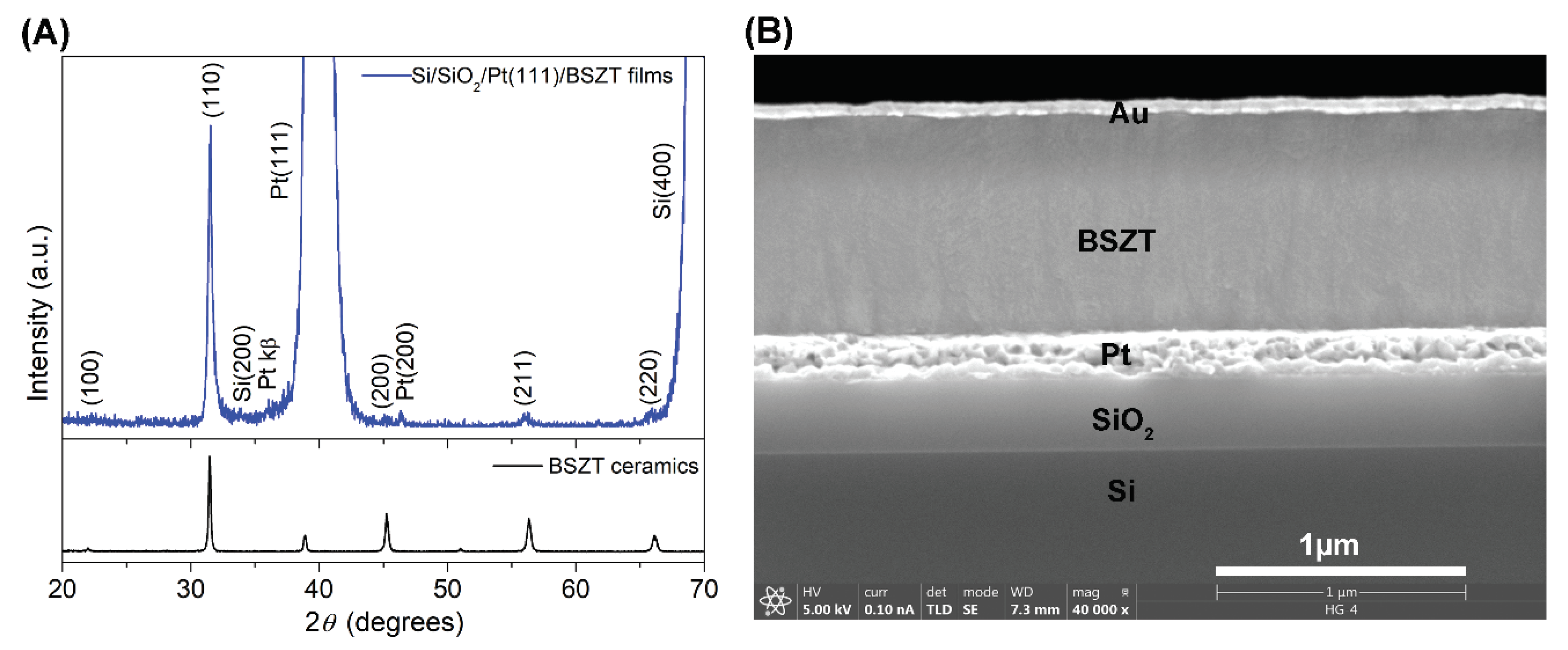
The X-ray diffraction (XRD) patterns of the BSZT films and BSZT ceramics are shown in Figure 1A. It is agreed that the detected XRD peaks are almost the same, which indicates the perovskite BSZT phase was clearly formed on the Si/SiO2/Pt(111) substrate. The deposited films have a pure perovskite phase and no secondary phase is detected, confirming that the stable solid solution of BSZT is formed. The cross-section SEM photograph in Figure 1B shows that the prepared BSZT thin films show a dense, cracks-free, uniform microstructure, and the clear structure of the Pt/BSZT/Au thin film capacitor is visible. The thickness of the prepared BSZT films is about 870 nm.
Figure 2 shows the capacitance properties of the BSZT films as a function of frequency, voltage, and temperature. As shown in Figure 2A, the prepared BSZT films show a weak frequency dispersion and a large capacitance density of 1.7 nF/mm2 at 100 kHz. It can be calculated that the dielectric constant (εr) is about 170, which is obviously higher than the reported STO films (~100). Therefore, a larger capacitance density higher than that of STO thin films could be achieved. In addition, the prepared BSZT films show a very low dielectric loss of 0.01, which is lower than the reported BST thin films [20]. The results reveal that the substitution of Ti with Zr can reduce the dielectric loss. The Direct Current (DC) voltage dependence of the capacitance density of the prepared films at the frequency of 100 kHz was measured from −40 V to 40 V in Figure 2B. The prepared films can withstand 40 V DC bias voltage. It was also noticed that the capacitance decreases with the voltage. This phenomenon is very prevalent in EIA Class II ceramic capacitor. For a better description of the stability of the capacitance under high operating voltage, the relative variation ratio of capacitance was plotted as a function of DC voltage in Figure 2C. This ratio is calculated by the change of the capacitance values under different DC operating voltages to that of 0 V DC. The EIA code does not take into consideration the DC voltage dependence in the Class II ceramics capacitor. According to the CENELEC Electronic Components Committee (CECC) code, the DC voltage dependence is less than −30% for the 2C1 class ceramics capacitor [21]. Therefore, the prepared BSZT films can satisfy this standard when the rated voltage is less than 40 V. The temperature dependence of capacitance in the testing range of 30~180 °C is shown in Figure 2D. The prepared capacitance exhibits an almost linear and small change (ΔC/C ~13.6%) of capacitance from 30 to 180 °C. According to the EIA code, the BSZT thin film capacitor can satisfy the requirement from most Class II ceramics with first letter code of Z.
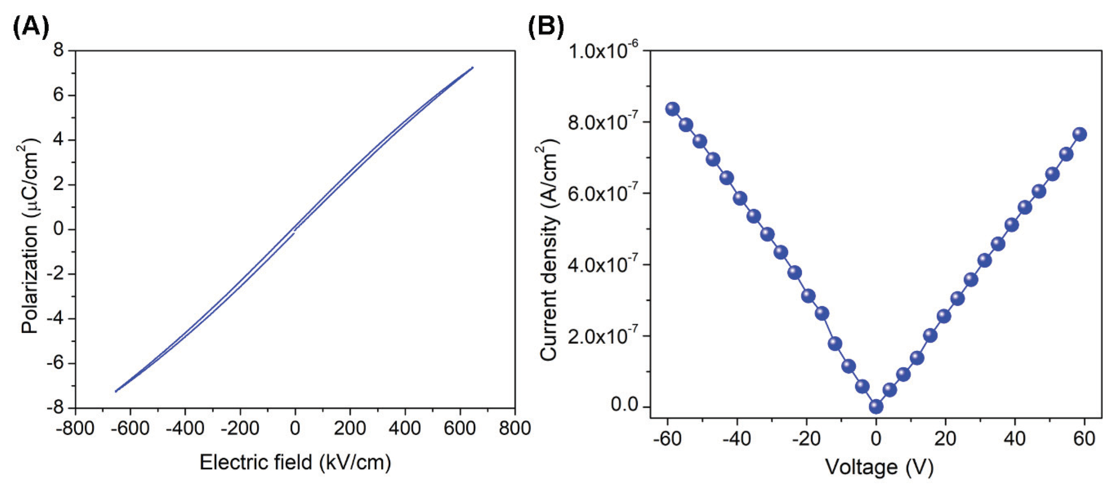
Figure 3A shows the polarization electric field (P-E) hysteresis loop and the leakage current behavior of the BSZT thin films. The P-E loops of the prepared BSZT films possess good linearity and weak ferroelectric behavior, which indicate the obvious characteristics of paraelectric thin films. Figure 3B shows the leakage current density of the thin films as a function of the applied bias electrical field from −60 V to 60 V. The leakage current density of the films linearly increases with the applied bias range, which indicates good ohmic conduction in the films. More importantly, the current density is about 7.65 × 10⁻⁷ A/cm2 at 60 V, which is lower than that of BST films.
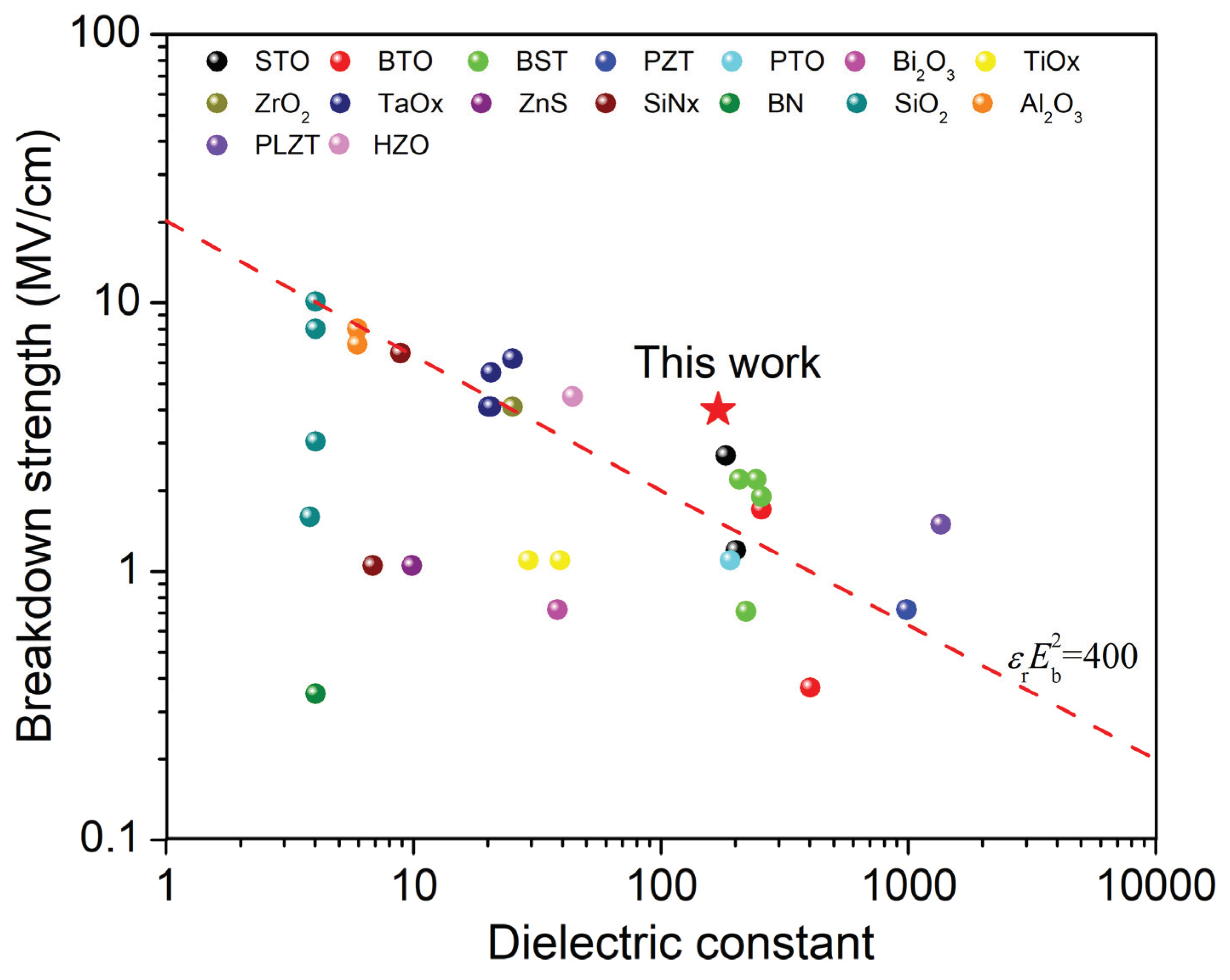
The electrical performance of a dielectric capacitor is determined mainly by the electric breakdown field (Eb) and dielectric constants (εr) of the dielectric layers. It is very difficult to obtain a dielectric material with the simultaneous features of high εr and Eb since there is an inherent tradeoff between the εr and the Eb for a dielectric material [2]. There is an equation used to describe the relationship between εr and Eb:
This experimental constant is given as 400 when Eb is expressed in megavolts per centimeter (MV/cm). The εr of most dielectric films is not more than 400. Figure 4 shows the Eb as a function of εr for a variety of dielectric thin-films [2,22,23]. In this work, the Eb of the BSZT thin film was about 4 MV/cm, which is higher than the reported STO and BST films. Therefore, εr is higher than the constant. This result shows that the BSZT films are a very potential dielectric material for the thin filmcapacitor application in many performance parameters.
4. Conclusions
In this work, high-quality BSZT thin films were successfully prepared on a Si/SiO2/Pt(111) substrate. The prepared perovskite BSZT film also showed a high capacitance density of 1.7 nF/mm2 at 100 kHz and a very low dielectric loss of 0.01 at 100 kHz. The prepared BSZT thin films also display a very low leakage current density (7.65 × 10⁻⁷ A/cm2 at 60 V) and high electric breakdown strength (~4 MV/cm). The results indicate that the BSZT thin film shows great potential for coupling and decoupling thin filmcapacitor applications.
Author Contributions
Conceptualization, P.Y.; methodology, X.C.; investigation, X.C., T.M., B.H., and Y.L.; data curation, X.C.; writing—original draft preparation, X.C.; writing—review and editing, P.Y.; project administration, P.Y.; funding acquisition, P.Y. All authors have read and agreed to the published version of the manuscript.
Funding
This research was funded by the National Natural Science Foundation of China under grant No. u1601208 and No. 51802204, China.
Acknowledgments
We appreciate Wang Hui from the Analytical and Testing Center of Sichuan University for her help with SEM characterization.
Conflicts of Interest
The authors declare no conflicts of interest.
References
- Chen, X.; Zhang, Y.; Xie, B.; Huang, K.; Wang, Z.; Yu, P. Thickness-Dependence of growth rate, dielectric response, and capacitance properties in Ba0.67Sr0.33TiO3/LaNiO3 hetero-structure thin films for film capacitor applications. Thin Solid Films 2019, 685, 269–274. [Google Scholar] [CrossRef]
- Johari, H.; Ayazi, F. High-Density Embedded Deep Trench Capacitors in Silicon with Enhanced Breakdown Voltage. IEEE Trans. Compon. Packag. 2010, 32, 808–815. [Google Scholar] [CrossRef]
- Perng, T.H.; Chien, C.H.; Chen, C.W.; Lehnen, P.; Chang, C.Y. High-Density MIM capacitors with HfO2 dielectrics. Thin Solid Films 2004, 469, 345–349. [Google Scholar] [CrossRef]
- Tuichai, W.; Danwittayakul, S.; Maensiri, S.; Thongbai, P. Investigation on temperature stability performance of giant permittivity (In + Nb) in co-Doped TiO2 ceramic: a crucial aspect for practical electronic applications. Rsc. Adv. 2016, 6, 5582–5589. [Google Scholar] [CrossRef]
- Pan, M.-J.; Randall, C.A. A brief introduction to ceramic capacitors. IEEE Electr. Insul. Mag. 2010, 26, 44–50. [Google Scholar] [CrossRef]
- Sugii, N.; Yamada, H.; Kagaya, O.; Yamasaki, M.; Sekine, K.; Yamashita, K.; Watanabe, M.; Murakami, S. High-Frequency properties of SrTiO3 thin-film capacitors fabricated on polymer-Coated alloy substrates. Appl. Phys. Lett. 1998, 72, 261–263. [Google Scholar] [CrossRef]
- Kozyrev, A.; Samoilova, T.; Golovkov, A.; Hollmann, E.; Kalinikos, D.; Loginov, V.; Prudan, A.; Soldatenkov, O.; Galt, D.; Mueller, C. Nonlinear behavior of thin film SrTiO3 capacitors at microwave frequencies. J. Appl. Phys. 1998, 84, 3326–3332. [Google Scholar] [CrossRef]
- Finstrom, N.H.; Gannon, J.A.; Pervez, N.K.; York, R.A.; Stemmer, S. Dielectric losses of SrTiO3 thin film capacitors with Pt bottom electrodes at frequencies up to 1 GHz. Appl. Phys. Lett. 2006, 89, 242910. [Google Scholar] [CrossRef] [Green Version]
- Konofaos, N.; Evangelou, E.; Wang, Z.; Helmersson, U. Properties of Al-SrTiO3-ITO capacitors for microelectronic device applications. IEEE Trans. Electron Devices 2004, 51, 1202–1204. [Google Scholar] [CrossRef]
- Takemura, K.; Kikuchi, K.; Ueda, C.; Baba, K.; Aoyagi, M.; Otsuka, K. SrTiO3 thin film decoupling capacitors on Si interposers for 3D system integration. In Proceedings of the 2009 IEEE International Conference on 3D System Integration, San Francisco, CA, USA, 28–30 September 2009; pp. 1–5. [Google Scholar]
- Takemura, K.; Ohuchi, A.; Shibuya, A. Si interposers integrated with SrTiO3 thin film decoupling capacitors and through-Si-vias. In Proceedings of the 2008 IEEE 9th VLSI Packaging Workshop of Japan, Kyoto, Japan, 1–2 December 2008; pp. 127–130. [Google Scholar]
- Jain, P.; Rymaszewski, E.J. Embedded thin film capacitors-Theoretical limits. IEEE Trans. Adv. Packag. 2002, 25, 454–458. [Google Scholar] [CrossRef]
- Chan, N.; Wang, D.; Wang, Y.; Dai, J.; Chan, H. The structural and in-Plane dielectric/ferroelectric properties of the epitaxial (Ba, Sr)(Zr, Ti)O3 thin films. J. Appl. Phys. 2014, 115, 234102. [Google Scholar] [CrossRef]
- Fu, S.L.; Ho, I.C.; Chen, L.S. Studies on semiconductive (Ba0.8Sr0.2)(Ti0.9Zr0.1)O3 ceramics. J. Mater. Sci. 1990, 25, 4042–4046. [Google Scholar] [CrossRef]
- Jiang, L.; Tang, X.; Jiang, Y.; Liu, Q.; Ma, C.; Chan, H. Epitaxial growth and dielectric properties of BSZT thin films on SrTiO3: Nb single crystal substrate prepared by pulsed laser deposition. Surf. Coat. Technol. 2013, 229, 162–164. [Google Scholar] [CrossRef]
- Fan, Y.; Yu, S.; Sun, R.; Li, L.; Yin, Y.; Du, R. Microstructure and electrical properties of Ba0.7Sr0.3(Ti1−xZrx)O3 thin films prepared on copper foils with sol–gel method. Thin Solid Films 2010, 518, 3610–3614. [Google Scholar] [CrossRef]
- Sharma, S.; Ram, M.; Thakur, S.; Sharma, H.; Negi, N.S. Structural Studies of Zirconium Doped Ba0.70Sr0.30TiO3 Lead Free Ferroelectric Thin Films. Aip Conf. Proc. 2016, 1728, 020192. [Google Scholar]
- Zhai, J.; Yao, X.I.; Chen, H. Structural and dielectric properties of (Ba0.85Sr0.15)(Zr0.18Ti0.82)O3 thin films grown by a sol–gel process. Ceram. Int. 2004, 30, 1237–12403. [Google Scholar] [CrossRef]
- Tang, X.; Jie, W.; Chan, L.W. Dielectric properties of columnar-grained (Ba0.75Sr0.25)(Zr0.25Ti0.75)O3 thin films prepared by pulsed laser deposition. J. Cryst. Growth 2005, 276, 453–457. [Google Scholar] [CrossRef]
- Chen, X.; Yang, C.; Zhang, X.; Li, J.; Liu, H.; Xiao, D.; Yu, P. The Effects of Buffers on the Microstructure and Electrical Properties of Mn/Y Co-Doped Ba0.67Sr0.33TiO3 Thin Films. Integr. Ferroelectr. 2012, 140, 132–139. [Google Scholar] [CrossRef]
- ABC of CLR in European Passive Components Institute (EPCI) Home Page. Available online: https://epci.eu/category/abc-of-clr/ (accessed on 26 March 2020).
- Park, M.H.; Kim, H.J.; Kim, Y.J.; Moon, T.; Kim, K.D.; Hwang, C.S. Thin HfxZr1−xO2 films: a new lead-Free system for electrostatic supercapacitors with large energy storage density and robust thermal stability. Adv. Energy Mater. 2014, 4, 1400610. [Google Scholar] [CrossRef]
- Ma, B.; Hu, Z.; Koritala, R.E.; Lee, T.H.; Dorris, S.E.; Balachandran, U. PLZT film capacitors for power electronics and energy storage applications. J. Mater. Sci. Mater. Electron. 2015, 26, 9279–9287. [Google Scholar] [CrossRef]
Figure 1.
(A) The X ray-diffraction (XRD) patterns of the Ba0.3Sr0.7Zr0.18Ti0.82O3 (BSZT) films. (B) The cross-section scanning electron microscopy (SEM) photographs of the Pt/BSZT/Au thin film capacitor.
Figure 1.
(A) The X ray-diffraction (XRD) patterns of the Ba0.3Sr0.7Zr0.18Ti0.82O3 (BSZT) films. (B) The cross-section scanning electron microscopy (SEM) photographs of the Pt/BSZT/Au thin film capacitor.

Figure 2.
The capacitance properties of the BSZT films. (A) The capacitance density and dielectric loss as a function of frequency. (B) Direct Current (DC) voltage dependence of capacitance density and dielectric loss. (C) The relative variation ratio of capacitance density as a function of DC voltage. (D) The capacitance density as a function of testing temperature in the range of 30~180 °C.

Figure 3.
(A) The polarization-electric field (P-E) hysteresis loops measured at 100 Hz. (B) Leakage current density of the BSZT thin film capacitor as a function of the applied bias voltage at room temperature.
Figure 3.
(A) The polarization-electric field (P-E) hysteresis loops measured at 100 Hz. (B) Leakage current density of the BSZT thin film capacitor as a function of the applied bias voltage at room temperature.

Figure 4.
Electric breakdown field (Eb) as a function of dielectric constants (εr) for a variety of the dielectric thin-films. The data are from previously published literature.
Figure 4.
Electric breakdown field (Eb) as a function of dielectric constants (εr) for a variety of the dielectric thin-films. The data are from previously published literature.

© 2020 by the authors. Licensee MDPI, Basel, Switzerland. This article is an open access article distributed under the terms and conditions of the Creative Commons Attribution (CC BY) license (http://creativecommons.org/licenses/by/4.0/).
Share and Cite
MDPI and ACS Style
Chen, X.; Mo, T.; Huang, B.; Liu, Y.; Yu, P. Capacitance Properties in Ba0.3Sr0.7Zr0.18Ti0.82O3 Thin Films on Silicon Substrate for Thin Film Capacitor Applications. Crystals 2020, 10, 318. https://doi.org/10.3390/cryst10040318
AMA Style
Chen X, Mo T, Huang B, Liu Y, Yu P. Capacitance Properties in Ba0.3Sr0.7Zr0.18Ti0.82O3 Thin Films on Silicon Substrate for Thin Film Capacitor Applications. Crystals. 2020; 10(4):318. https://doi.org/10.3390/cryst10040318
Chicago/Turabian StyleChen, Xiaoyang, Taolan Mo, Binbin Huang, Yun Liu, and Ping Yu. 2020. "Capacitance Properties in Ba0.3Sr0.7Zr0.18Ti0.82O3 Thin Films on Silicon Substrate for Thin Film Capacitor Applications" Crystals 10, no. 4: 318. https://doi.org/10.3390/cryst10040318
Note that from the first issue of 2016, this journal uses article numbers instead of page numbers. See further details here.