Article

One-Step Fabrication of Inverted Pyramid Textured Silicon Wafers via Silver-Assisted Chemical Etching Combing with Synergism of Polyvinylpyrrolidone (PVP)

College of Materials Science & Engineering, Nanjing Tech University, 30 South PuZhu Road, Nanjing 211816, China
*
Author to whom correspondence should be addressed.
Crystals 2021, 11(5), 459; https://doi.org/10.3390/cryst11050459
Submission received: 2 April 2021 / Revised: 18 April 2021 / Accepted: 19 April 2021 / Published: 21 April 2021
(This article belongs to the Special Issue Low-Dimensional Materials for Electronic Device Applications)

Abstract

:
Inverted pyramid-texturing of silicon surface has been proven to have great application potential in silicon solar cells. In this paper, we utilized Ag-assisted chemical etching (Ag–ACE) technology combing with polyvinylpyrrolidone (PVP) to fabricate an inverted pyramid textured Si surface. We call it Ag@PVP–ACE. The effect of different experimental parameters on etching results was observed. We show that the microstructure of the Si surface exhibited two states as the concentration of NH4HF2 and PVP concentration changed: polishing and inverted pyramid texturing. Meanwhile, we found inverted pyramids easier to form at the high temperature and low H2O2 concentration of the etching system. Consequently, compared to inverted pyramid structures fabricated by nanostructure rebuilding (NSR) technology and Ag@PVP–ACE, we consider that Ag@PVP–ACE technology could become a viable strategy for fabricating inverted pyramid textured Si wafers in Si solar cells production.

1. Introduction

Light-trapping structure fabrication is an essential step in Si solar cell production [1,2,3]. The significant reduction of surface reflectivity enhances light absorption and thus improves the conversion efficiency of solar cells [4]. As reported in single crystalline silicon (sc-Si) solar cell with the conventional upright pyramid, normally, the average reflectivity is limited to 10–14% [5,6], it was difficult to further reduce the surface reflectivity of upright pyramid textured Si. Thus, the inverted pyramid has attracted the attention of many researchers due to its controllable low surface reflectivity and secondary reflection of light in the structure [7,8,9].
As a simple wet chemical etching method to fabricate micro/nanostructure of Si surface. More attention has been paid to metal-assisted chemical etching (MACE) in recent years [10]. Various structures of Si prepared by MACE have presented application potentials in fields ranging from solar cells [2,11,12], Si photoelectrodes [13], chemical and biological sensing [14,15,16,17], thermoelectric transform [18,19], Li-ion batteries [20,21,22], semiconductor micro/nano devices [23,24,25] and more. MACE has been involved local coupling of redox reactions, catalytically generated electric fields caused by bipolar electrochemical reaction and autonomous movement aroused from self-electrophoresis of noble metal particles [26]. It is acknowledged that H2O2 is reduced faster around silver nanoparticles. The holes (h+) are concentrated at the Si/Ag interface and injected from the metal into the silicon valence band [10,27]. The self-electrophoresis model reported by Peng and his coworkers was that the etching of the local Si layer around noble metal particles and the catalytic electric field further pushed the noble metal particles into the inner of Si wafers [28]. Ag [29,30] and Cu [31] are used as the most common catalysts in MACE. However, other catalysts have been reported, such as Pt [32], Pd [33], Au [34], C [35], etc. The commonly used oxidants in MACE are H2O2 [36] and HNO3 [37]. Other oxidants are rarely used, such as V2O5 [38].
It is worth mentioning that MACE is always used to fabricate the inverted pyramid structure of the Si surface [1,39]. The manufacturing process of an inverted pyramid can be divided into one-step and multistep methods. Du et al. utilized Cu particles to fabricate an inverted pyramid by a one-step method. They have reported that solution composition and concentration significantly affected the structure of Si surface, inverted pyramid, V-groove, hybrid structure, and upright pyramid were observed in the evolution of textured Si surface morphologies [40]. In addition, they considered that the anisotropic etching process, which resulted in the formation of an inverted pyramid, is mainly derived from noble metal particles that are easier to obtain electrons from {100} crystal planes than {111}. Thus, the difference of noble metal nanoparticle deposition density on different crystal planes resulted in the anisotropic characteristic of etching rate [40,41]. Nanostructure rebuilding (NSR) technology has been reported as a common multistep method to fabricate the inverted pyramid [5,8,42]. Deposited Ag particles accelerated the etching rate of the local Si layer to form nanopores, then utilized NSR treatment to fabricate the inverted pyramid via anisotropic etching [42,43].
In this paper, we fabricated the inverted pyramid of Si surface through Ag-assisted chemical etching technology combing with the synergism of polyvinylpyrrolidone (PVP), which we called Ag@PVP–ACE. As a safe and efficient etching agent, ammonium hydrogen difluoride (NH4HF2) was used to replace HF for rapidly etching SiO2 [44] in our work. Koker et al. [45] confirmed that the etching rate of HF2 is about 15 times faster than HF via the photoelectrochemical method. In addition, polyvinylpyrrolidone (PVP) is a well-known surfactant and stabilizer [46] that has attracted attention to its structure-directing characteristics of controlling the length and diameter of noble metal particles [47]. The critical factors in achieving polishing or fabricating inverted pyramid in Ag@PVP–ACE process were revealed, and a systematic investigation was performed to confirm the parameters condition of fabricating inverted pyramids in Ag@PVP–ACE process. We compared the microstructure obtained by Ag@PVP–ACE and NSR technology and analyzed the difference. Furthermore, the difference in optical properties between the structure of upright, inverted pyramids is revealed.

2. Materials and Methods

2.1. Materials

Diamond-wire-sawn (DWS) (100)-oriented p-type Si wafers (156.75 × 156.75 mm2, 180 ± 10 μm thickness, the resistivity of 0.5–1.5 Ω·cm) were employed in experiments, and all of above p-type silicon wafers were born-doped. Silver nitrate (AgNO3, AR), hydrogen peroxide (H2O2, 30%, GR) were obtained from Sinopharm Chemical. High purity deionized water with a resistivity of 18.25 MΩ·cm−1 was used in the experiment. Ammonium hydrogen fluoride (NH4HF2, AR) was purchased from Nanjing Chemical Reagent Co., Ltd. (Nanjing, China). Aqueous ammonia (NH3·H2O, 25%, AR) was purchased from Shanghai Ling Feng Chemical Reagent Co., Ltd. (Shanghai, China). Polyvinylpyrrolidone (PVP-K12/K30/K88-96, AR) was received from Shanghai Aladdin Biochemical Technology Co., Ltd. (Shanghai, China). All laboratory supplies were used as-received.

2.2. Experimental Method

A wet chemical etching aqueous solution containing AgNO3, H2O2 and NH4HF2 (Ag–ACE) along with the addition of polyvinylpyrrolidone (Ag@PVP–ACE) was used in our experiment. We explored the optimal conditions for fabricating inverted pyramid structure through a series of experiments with different parameters, as shown in Table 1.
DWS Si wafers were immersed vertically into the Ag@PVP–ACE solution for fabricating inverted pyramid textured surface. Then etched Si wafers were immersed into deionized water for 2 min. Moreover, the textured Si wafers were rinsed in NH3·H2O (0.1 M) solution with H2O2 (0.1 M) for 3 min to remove residual Ag particles. Afterward, Si wafers were rinsed in pure water for 30 s and HF (0.1 M) solution for 1 min to clean the residual aqueous ammonia. Consequently, rinsing the silicon wafer repeatedly with deionized water and drying.
The surface and cross-sectional morphologies of Si wafers were observed by field-emission scanning electron microscopy (FESEM, Hitachi, 4800) and scanning electron microscopy (SEM, JEOL, JSM-IT200). The sample’s reflectivity spectra in the wavelength range of 350–1050 nm were measured by UV-vis-NIR spectrophotometer (UV-3101PC, Japan, with an integrating sphere). The average reflectivity was calculated by measuring the reflectivity of nine areas evenly distributed on the surface of the Si wafer.

3. Results

As shown in Figure 1, etching results exhibited two completely different phenomena-fabrication of inverted pyramid or polishing. The object mirroring was completely invisible due to the existence of the inverted pyramid light-trapping structure on the Si surface; a clear object outline appeared on the polished Si surface (Figure 1a). Correspondingly, inverted pyramid textured prepared by Ag@PVP–ACE exhibited low reflectivity, the average reflectivity reached 8.31%, and the average reflectivity of Si surface polished by Ag@PVP–ACE reached 49.46%.

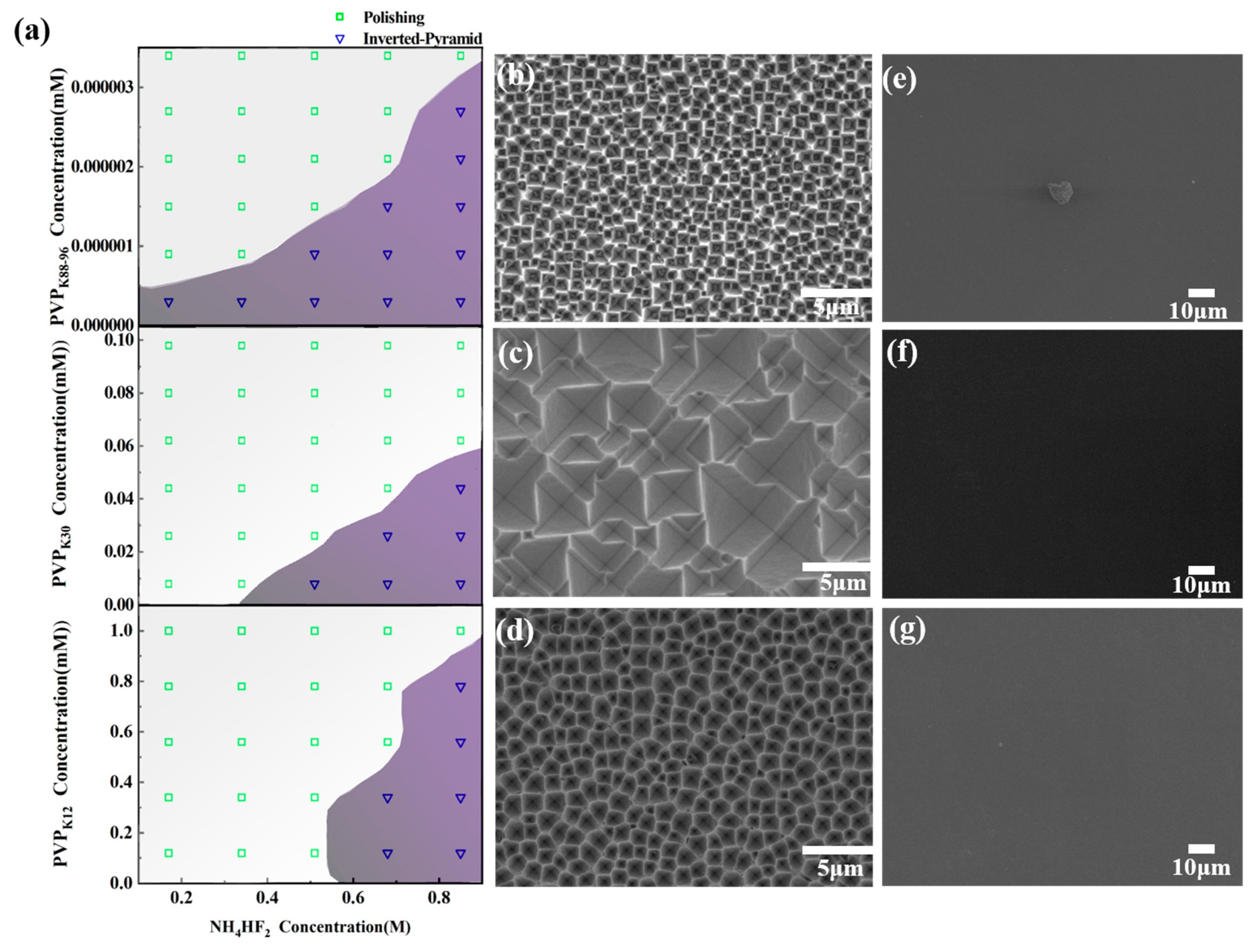
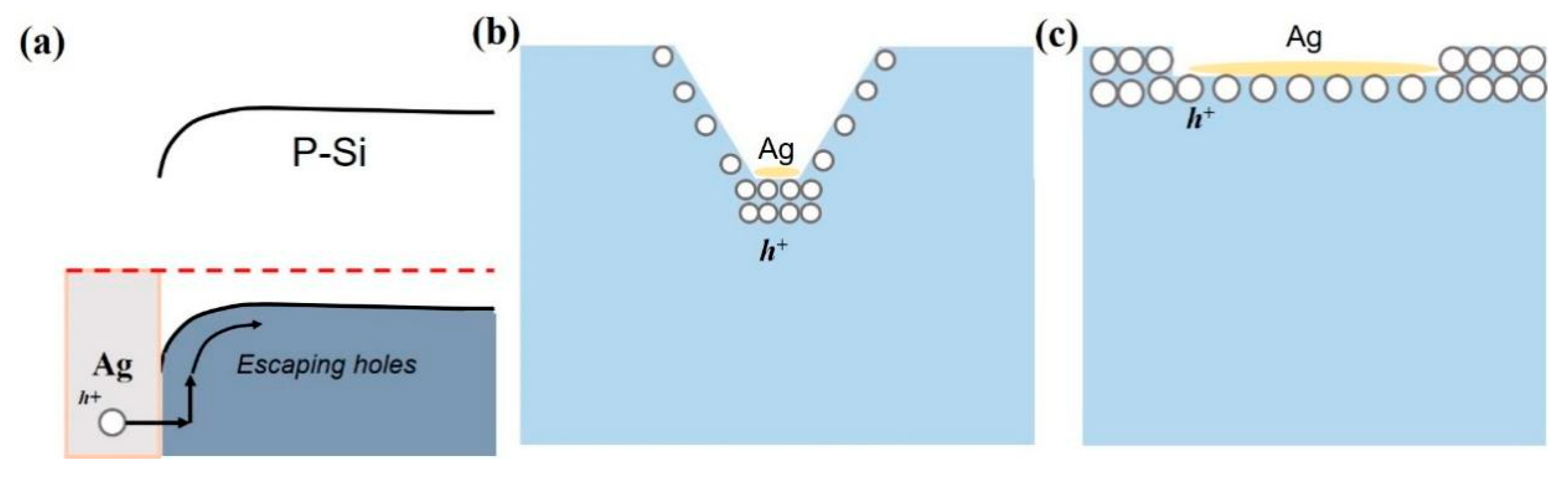
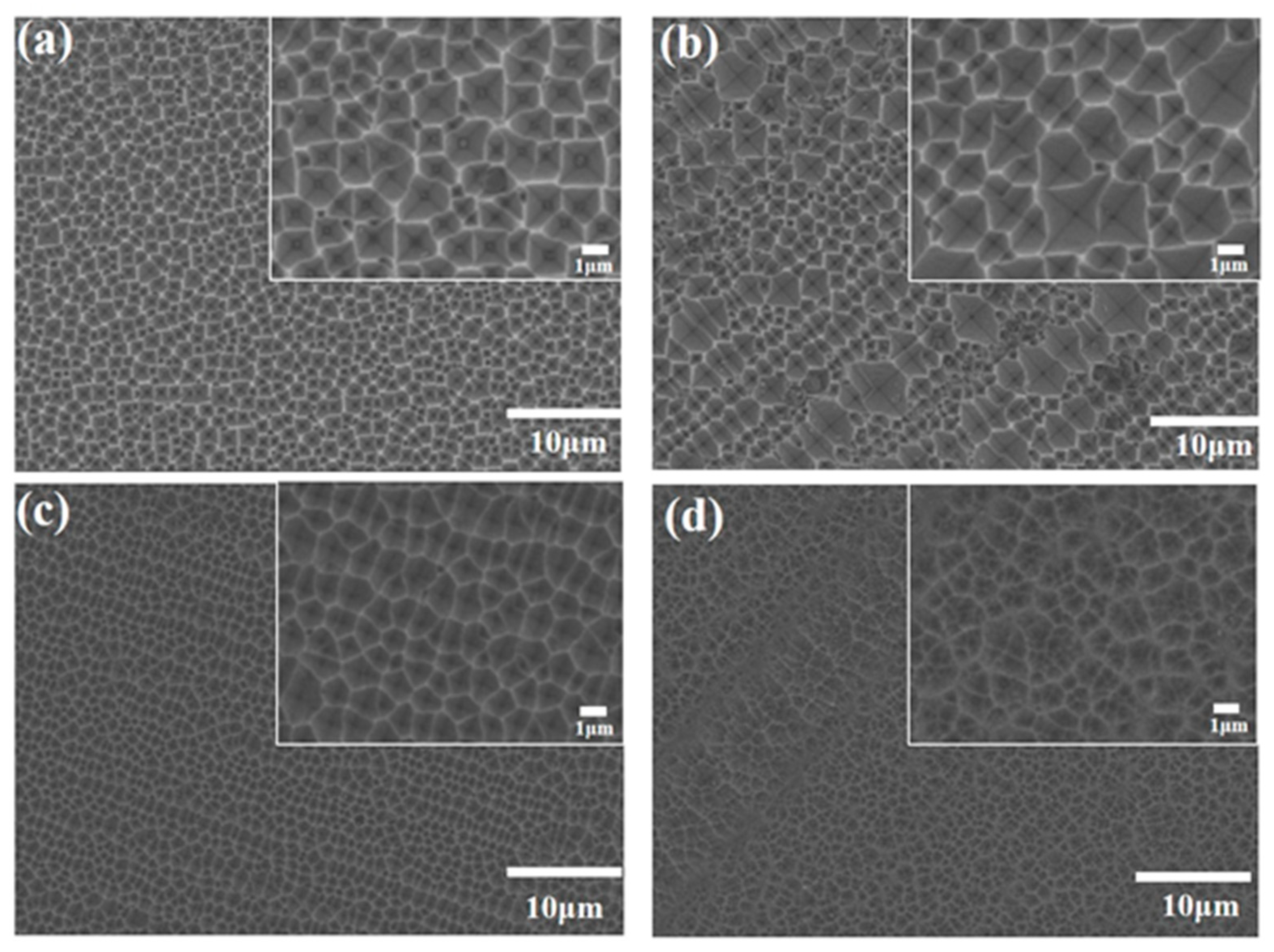
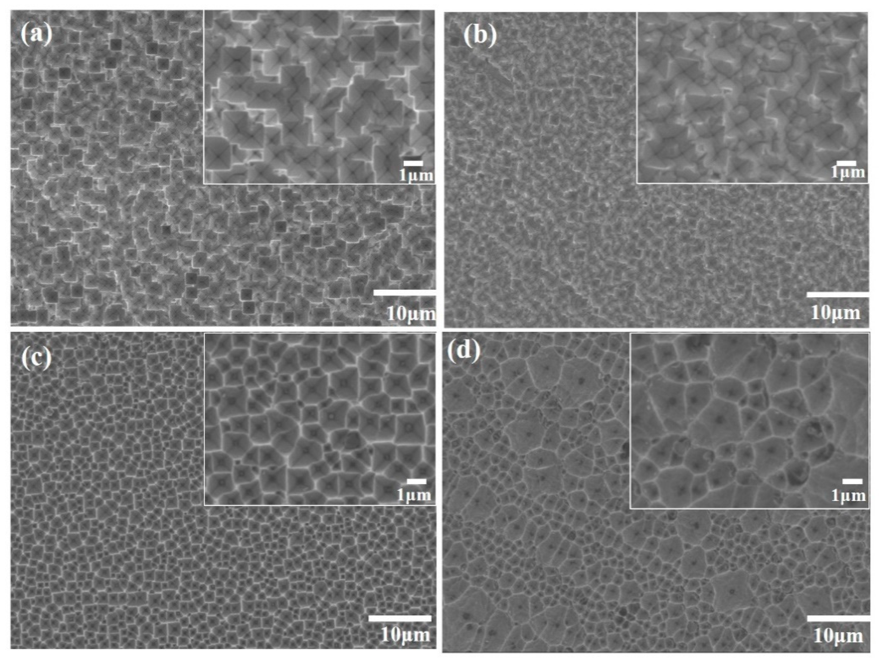
3.1. Effect of PVP and NH4HF2 Concentration on Etching Results in Ag@PVP-MACE

The etching results were related to NH4HF2 and PVP concentration in Ag@PVP–ACE solution, as shown in Figure 2a. The inverted pyramid (Figure 2b–d) was normally produced at low PVP concentration and high NH4HF2 concentration. A polished Si surface (Figure 2e–g) appeared under high PVP concentration and low NH4HF2 concentration. In addition, the polymer molecular weight of PVP in the solution significantly affected the etching results. The addition of K12 and K30 to an aqueous Ag–ACE solution was more inclined to manufacture a polished Si surface. However, under some circumstances, the addition of K88-96 in Ag–ACE was easier to manufacture the inverted pyramid structure on the Si surface. Thus, we utilized K88-96 to complete the subsequent experiments.
The transformation of the etching results was directly related to the absorption effect of PVP on Ag particles because PVP was more inclined to bind the {111} crystal plane of Ag particles [46,48]. The fabrication of inverted pyramids arose from the weak absorption effect of PVP when the PVP concentration was low. As PVP concentration increased, the adsorption effect of the PVP enhanced continuously, resulting in difficulty for single Ag particles to move directly into the inner of Si. Due to the steric hindrance of Ag@PVP, the vertical etching process of Ag@PVP–ACE became unapparent. Thus, the polishing process occurred. A high NH4HF2 concentration made it easier to generate the inverted pyramid structure, which was attributed to the transformation of etching behavior of Ag@PVP–ACE solution. A. M. Khort et al. observed that HF2 was different from F in etching mechanism, HF2 was conducive to the formation of porous silicon, but F was more inclined to occur plane-parallel etching [49]. With the increase of NH4HF2 concentration, the tendency of vertical etching that resulted from the amount of HF2 increase strengthened, which further weakened the effect of PVP. Therefore, a higher NH4HF2 concentration was more conducive to the fabrication of an inverted pyramid. At this moment, the NH4HF2 concentration played a leading role in the Ag@PVP–ACE process.

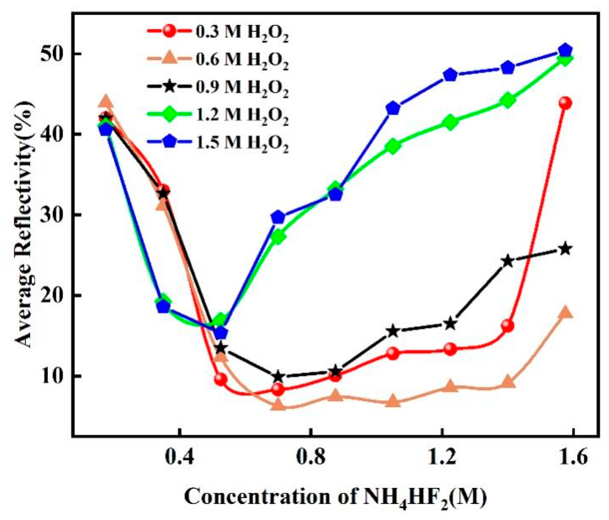
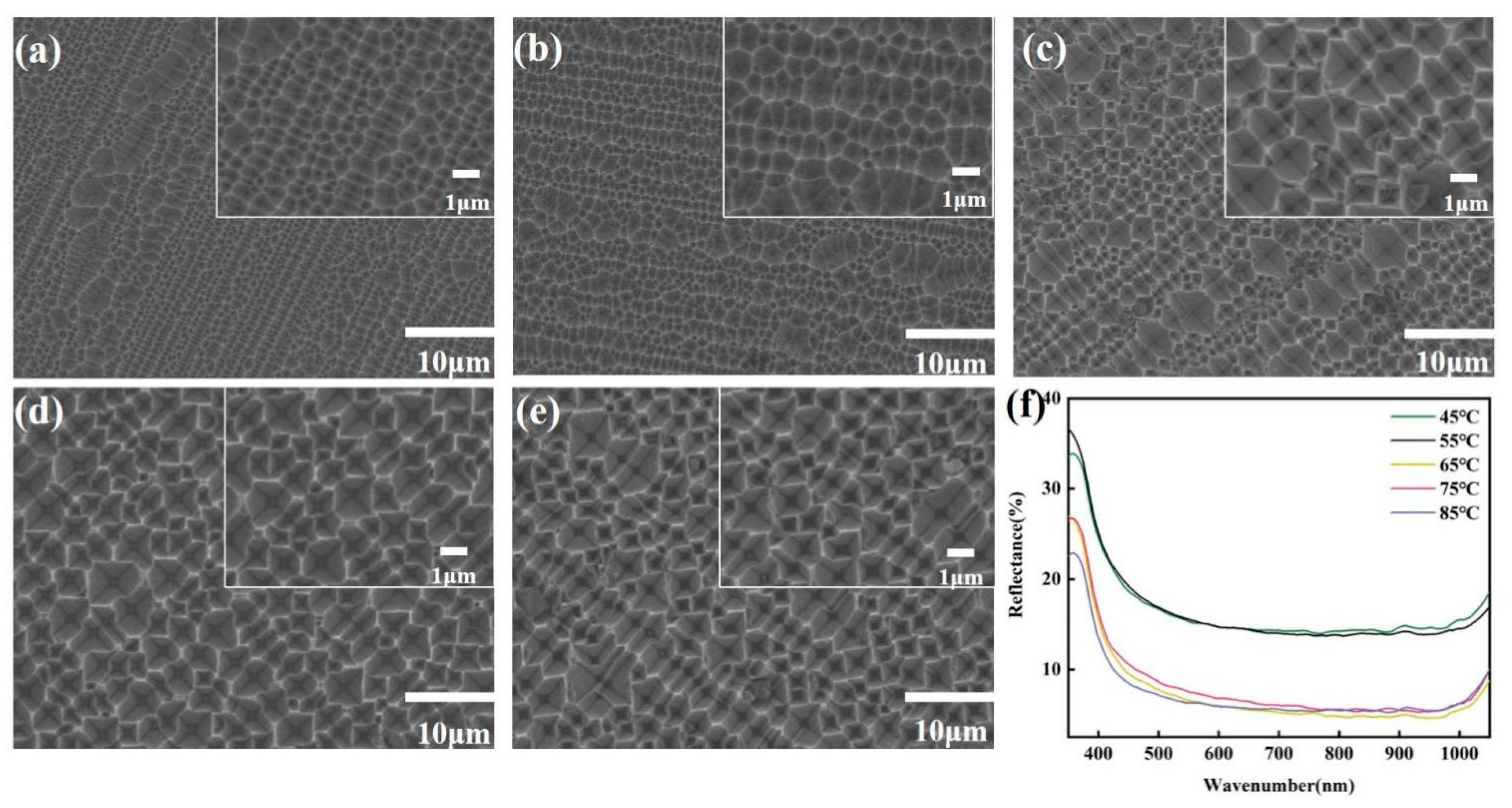
3.2. Effect of H2O2 Concentration on Etching Results in Ag@PVP–ACE

Figure 3 illustrates the dependence of samples surface average reflectivity on the concentration of H2O2 and NH4HF2. It can be clearly observed that as the concentration of NH4HF2 increased continuously, the surface reflectance first decreased and then increased. When the concentration of NH4HF2 was 0.175 M, the surface reflectivity etched by different H2O2 concentrations in solution was above 40%. When the concentration of NH4HF2 in the solution reached 0.35 M, the surface reflectivity reduced to 33% at low H2O2 concentration (0.3–0.9 M), while at high H2O2 concentration (1.2–1.5 M), the Si surface reflectance reduced to less than 20%. It is worth mentioning that etched Si surface average reflectivity increased as NH4HF2 concentration improved when the H2O2 concentration of the solution was 1.2–1.5 M. However, a similar situation did not appear when the H2O2 concentration was 0.3–0.9 M. The surface reflectivity did not change much as the NH4HF2 concentration increased to 1.05 M. Afterward, average reflectivity of the etched Si surface slowly raised as NH4HF2 concentration improved.
Figure 4 shows the corresponding SEM images of samples etched by Ag@PVP–ACE with different H2O2 concentrations under 0.175 M NH4HF2. When the H2O2 concentration was 0.3 M, some large-sized shallow square grooves appeared on the Si surface, and the overall morphology was relatively flat (Figure 4a). The surface morphology became flatter when the concentration of H2O2 was 0.6 M (Figure 4b). However, the difference was that the shallow round groove was generated when H2O2 concentration increased to 1.2–1.5 M (Figure 4c,d). The process of transforming square groove to round groove means that anisotropy of the etching process was weakened as NH4HF2 concentration increased.
As for p-type Si, it was difficult to confine the holes under the Ag/Si contact interface. The holes would drift away from the p-type Si surface via the effect of the interface catalytic electric field (Figure 5a). Thus, the hole distribution density of different parts of the Si was obviously different. An anisotropy etching process of MACE occurred [27] (Figure 5b). With the increase of H2O2 concentration, ultra-high H2O2 concentration would inject additional holes into the Si valance band. The difference of holes distribution density reduced. As a result, anisotropic etching was weakened. By contrast, the isotropic etching process enhanced, the transformation of the square groove to round groove occurred via the etching behavior of Ag@PVP–ACE changes (Figure 5c).
The samples treated in 0.875 M NH4HF2-Ag@PVP–ACE with different H2O2 concentrations are shown in Figure 6. Large-scale inverted pyramid randomly distributed on the Si surface when H2O2 concentration was 0.3–0.6 M (Figure 6a,b), and inverted pyramid structure became shallow as H2O2 concentration increase to 1.2–1.5 M (Figure 6c,d). The above experimental results indicated that excessive H2O2 concentration did not apply to the formation of an inverted pyramid, whose average reflectivity was difficult to reduce effectively to less than 10% (Figure 3). As mentioned before, the increase of NH4HF2 concentration accelerated the formation of pores. However, there was a certain balance between oxidation rate and etching rate. The appearance of a shallow inverted pyramid was caused by an intense oxidation process and low SiO2 etching rate.

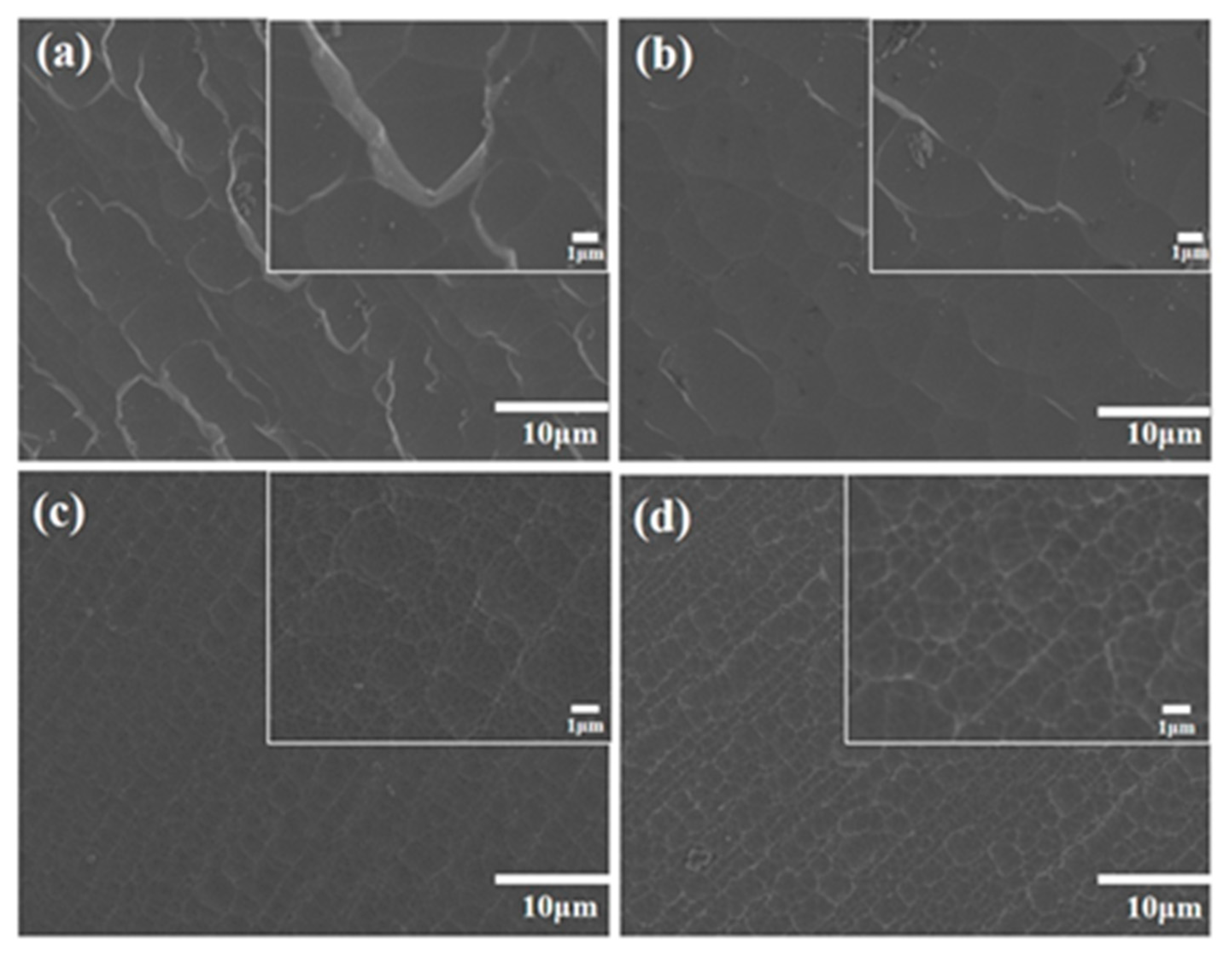
3.3. Effect of Temperature on Etching Results in Ag@PVP–ACE

Figure 7 shows the effect of etching temperature on the surface morphology of the DWS-Si wafers treated in Ag@PVP–ACE. The inverted pyramid structure fabricated at 45–55 °C was clearly shallow, and the four side edges of the inverted pyramid were blurred (Figure 7a,b). As the etching temperature increased to 65 °C, the depth of the inverted pyramid increased, and the four side edges were clearly distinguishable (Figure 7c–e). Results of reflectance spectrum were interrelated to surface morphology (Figure 7f), the reflectivity of Si wafers etched at 45–55 °C was significantly higher than the Si surface obtained by high-temperature (65–85 °C). It seems that NH4HF2 activity in the solution is positively related to temperature, but the oxidizing ability of H2O2 is rarely affected by the temperature. Under equal solution conditions, the etching process at low-temperature was dominated by H2O2. It is acknowledged that there was an obvious difference in the thickness of the thermal oxide layer on different Si crystal planes [50]. It was difficult for the low reactivity of NH4HF2 to completely remove the oxide layer of each crystal plane, which resulted in the appearance of a shallow inverted pyramid. The high etching rate of NH4HF2 could effectively remove the oxide layer of different crystal planes with increasing etching temperature. Namely, the etching rate was faster than the oxidation rate, which resulted in the anisotropic etching behavior of Ag@PVP–ACE enhanced. Hence, it was easier to generate the inverted pyramid with a high aspect ratio at high-temperature.

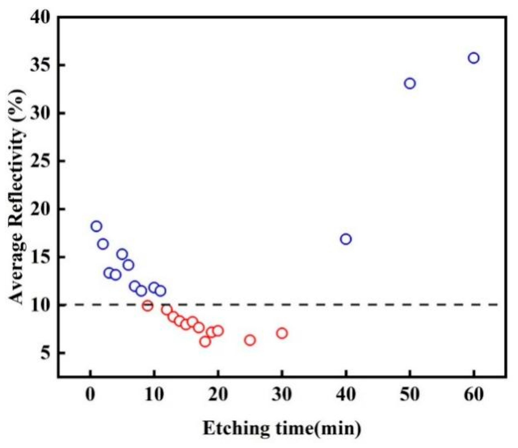
3.4. Effect of Time on Etching Results in Ag@PVP–ACE

The effect of time on the etching results is shown in Figure 8. It is obvious that the average reflectivity of Si wafers first decreased and then increased with prolonging etching time. The reflectivity of samples etched for 10–30 min was lower than 10%. Combing with the above experiment results, we considered that 0.6 M H2O2 was most beneficial for the inverted pyramid texturing process. With the above parameter conditions at this moment, NH4HF2 concentration (Figure 3) and temperature changes (Figure 7f) had little effect on the surface reflectivity after etching.

4. Discussion

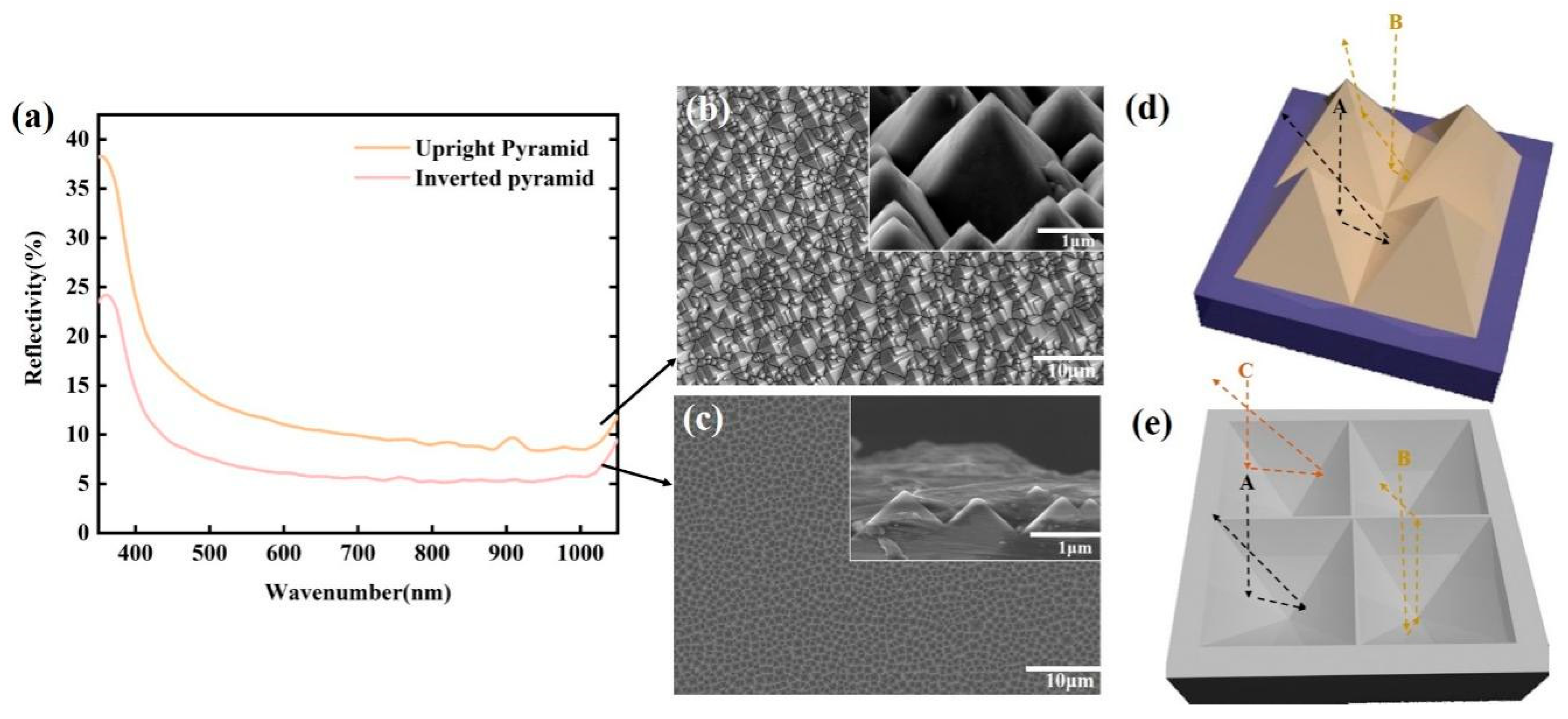
4.1. Comparative Analysis of NSR and Ag@PVP–ACE Technology for Fabricating Inverted Pyramid

We compared the inverted pyramid formation process of NSR treatment and Ag@PVP–ACE, as shown in Figure 9. As for the fabrication process of inverted pyramids in Ag@PVP–ACE, first, shallow inverted pyramid grooves appeared locally on the Si surface via anisotropic etching (Figure 9a), then dense inverted pyramid grooves distributed randomly on the Si surface (Figure 9b). As the etching process continued, large-sized inverted pyramid holes emerged (Figure 9c). Completely different from Ag@PVP–ACE was that many nanopores needed to be manufactured on the Si surface first, before NSR treatment (Figure 9d). During the NSR treatment, nanopores expanded (Figure 9e) and then inverted pyramid formed via anisotropic etching (Figure 9f). The above results are consistent with the phenomenon in Figure 8. What was completely different from NSR technology was that the surface reflectivity decreased from high to low at the initial etching stage (0–15 min) of Ag@PVP–ACE. However, the reflectivity of Si treated by NSR technology would first decrease and then increase. Due to the difference in etching behavior in NSR and Ag@PVP–ACE, the appearance of many nanopores resulted in low surface reflectivity at the beginning of the texturing process. Afterward, the formation of a large-sized inverted pyramid structure via anisotropic etching increased the surface reflectivity in the NSR process (Figure 9g). As for the Ag@PVP–ACE technology, nanopores were replaced by shallow inverted pyramid square grooves on the Si surface. The relatively smooth surface resulted in higher surface reflectivity at the beginning of the etching process. Subsequently, the depth and distribution density of many inverted pyramid structures whose increased, and the inverted pyramid grooves transformed to inverted pyramid pores, which resulted in a gradual decrease in reflectivity (Figure 9h).
As shown in Figure 10, the inverted pyramid after NSR treatment was regular and square holes (Figure 10a). However, the uneven distribution of inverted pyramid structure led to a significant difference in structure size. The size of the structure was mainly distributed in 0.2–0.6 μm and 1–1.2 μm (Figure 10c). The inverted pyramid prepared by Ag@PVP–ACE exhibited uniform and relatively flat textured Si surface (Figure 10b), the size of structure mainly distributes in 1.5–2.0 μm, and the distribution characteristics were more similar to the normal distribution (Figure 10d).
The significant difference in the size distribution of the inverted pyramid structure treated by NSR technology can be attributed to the inconsistent depth of the nanopores, as shown in Figure 11a. It is difficult to regulate the depth of nanopores in the MACE process. Thus, under the same etching rate, nanopores with smaller depth would preferentially form an inverted pyramid, while nanopores with the larger depth needed to remove more Si layer from the hole walls to form regular inverted pyramid (Figure 11b), inverted pyramids with different depths appeared on the surface of Si wafers (Figure 11c).
During the process of transforming deep nanopores into a complete inverted pyramid structure, the inverted pyramid structure formed by shallow pores was easily damaged due to further etching, which made the etching process difficult to control. The etching process needed to be controlled more precisely to obtain the ideal inverted pyramid structure (Figure 12a) in the NSR process, prolonged etching process led to the destruction of a large number of an inverted pyramid, and the inverted pyramid was replaced by an upright pyramid on the Si surface (Figure 12b). Because no nanopores were fabricated on the Si surface at the initial Ag@PVP–ACE stage, the inverted pyramids were almost formed on a similar plane. Thus, the inverted pyramid fabricated in the Ag@PVP–ACE process was more uniform in size and distribution (Figure 12c). Furthermore, increasing etching time would only cause the inverted pyramid to shallower, but the shape remained unchanged (Figure 12d).

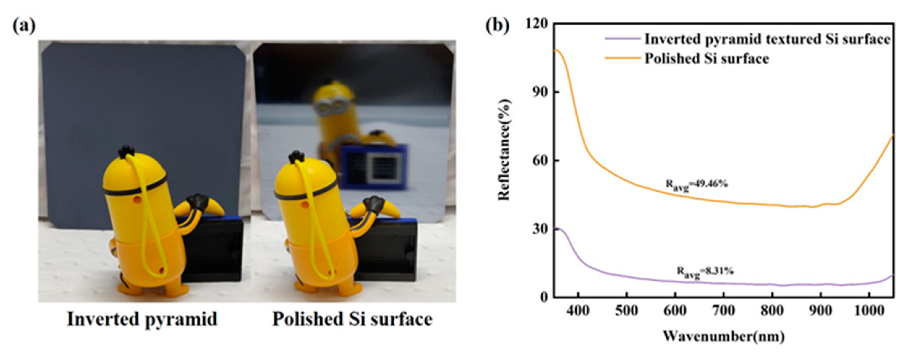
4.2. Comparative Analysis of the Optical Properties of Upright Pyramid and the Inverted Pyramid

The Si surface reflectivity of the inverted pyramid was significantly lower than that of an upright pyramid, as shown in Figure 13a. As for the randomly distributed upright pyramid (Figure 13b,d), 89% of incident rays suffered a double bounce (path A), and 11% occurred a triple bounce [51] (path B). However, the reflection paths of the randomly distributed inverted pyramid (Figure 13c) increased from two to three, the rays incident on the pyramid at smaller angles (path C) and 42% of incident rays suffered triple bounces [52,53]. The higher reflection frequency effectively reduced the surface reflectivity. Correspondingly, the energy mostly gathered inside the inverted pyramid, which had stronger energy collection efficiency [5].

5. Conclusions

In this paper, an efficient fabrication method for inverted pyramids of Si wafers by silver ion-assisted chemical etching with the synergism of PVP was investigated. The etching behavior with the addition of PVP into Ag–ACE solution exhibited two statuses: polishing or fabricating inverted pyramid. The critical factors for fabricating microstructure were demonstrated. The effect of various experimental parameters on the etching results in Ag@PVP–ACE was verified. Furthermore, we compared the inverted pyramid obtained by NSR technology and Ag@PVP–ACE, and the advantages of Ag@PVP–ACE were analyzed. Consequently, as a simple and low-cost one-step method to fabricate an inverted pyramid, we believe that the Ag@PVP–ACE process is a powerful solution with its simplicity and stability and may have application potential in solar cell, Si photoelectrode sensor, optical element and superhydrophobic surface. In addition, we hope that our work could provide a new strategy for utilizing organic molecules to control the etching behavior of the Ag/Si interface in the MACE solution.

Author Contributions

Y.L.: Conceptualization, investigation, data processing, writing—original draft. K.D.: revision, characterization. L.B.: grammar. Z.G.: formal analysis, funding acquisition, supervision, project administration, writing—review and editing. All authors have read and agreed to the published version of the manuscript.

Funding

This research was funded by the Jiangsu Collaborative Innovation Center for Advanced Inorganic Function Composites, the Priority Academic Program Development of Jiangsu Higher Education Institutions (PAPD).

Data Availability Statement

Not applicable.

Acknowledgments

This work was supported by funding of Jiangsu Collaborative Innovation Center for Advanced Inorganic Function Composites, the Priority Academic Program Development of Jiangsu Higher Education Institutions (PAPD) and Nanjing Naxin New Material Co., Ltd. (Nanjing, Jiangsu, China).

Conflicts of Interest

We would like to declare on behalf of my co-authors that the work described was original research that has not been published previously and not under consideration for publication elsewhere, in whole or in part. All the authors listed have approved the manuscript that is enclosed. No conflict of interest exists in the submission of this manuscript, and the manuscript is approved by all authors for publication.

References

  1. Wang, Y.; Yang, L.; Liu, Y.; Mei, Z.; Chen, W.; Li, J.; Liang, H.; Kuznetsov, A.; Xiaolong, D. Maskless inverted pyramid texturization of silicon. Sci. Rep. 2015, 5, 10843. [Google Scholar] [CrossRef] [PubMed] [Green Version]
  2. Liu, Y.; Lai, T.; Li, H.; Wang, Y.; Mei, Z.; Liang, H.; Li, Z.; Zhang, F.; Wang, W.; Kuznetsov, A.Y.; et al. Nanostructure formation and passivation of large-area black silicon for solar cell applications. Small 2012, 8, 1392–1397. [Google Scholar] [CrossRef] [PubMed]
  3. Yang, X.; Zhang, W.; Choi, J.; Ta, H.Q.; Bai, Y.; Chen, L.; Zhang, M.; Chen, Y.; Guan, Z.; Rummeli, M.H.; et al. Influence of bowl-like nanostructures on the efficiency and module power of black silicon solar cells. Sol. Energy 2019, 189, 67–73. [Google Scholar] [CrossRef]
  4. Zhang, P.; Jia, R.; Tao, K.; Jiang, S.; Dai, X.; Sun, H.; Jin, Z.; Ji, Z.; Liu, X.; Zhao, C.; et al. The influence of Ag-ion concentration on the performance of mc-Si silicon solar cells textured by metal assisted chemical etching (MACE) method. Sol. Energy Mater. Sol. Cells 2019, 200, 109983. [Google Scholar] [CrossRef]
  5. Zhang, C.; Chen, L.; Zhu, Y.; Guan, Z. Fabrication of 20.19% Efficient Single-Crystalline Silicon Solar Cell with Inverted Pyramid Microstructure. Nanoscale Res. Lett. 2018, 13, 91. [Google Scholar] [CrossRef] [PubMed] [Green Version]
  6. Mrazkova, Z.; Sobkowicz, I.P.; Foldyna, M.; Postava, K.; Florea, I.; Pištora, J.; Roca i Cabarrocas, P. Optical properties and performance of pyramidal texture silicon heterojunction solar cells: Key role of vertex angles. Prog. Photovolt. Res. Appl. 2018, 26, 369–376. [Google Scholar] [CrossRef]
  7. Han, S.J.; Ghosh, S.; Abudayyeh, O.K.; Hoard, B.R.; Culler, E.C.; Bonilla, J.E.; Han, S.M.; Han, S.E. Symmetry-breaking nanostructures on crystalline silicon for enhanced light trapping in thin film solar cells. Opt. Express 2016, 24, 1586–1596. [Google Scholar] [CrossRef] [PubMed]
  8. Gu, H.; Guan, Z.; Liu, Y. Large-scale preparation of 22.06% efficiency single-crystalline silicon solar cells with inverted pyramid microstructure through nanostructure rebuilding treatment. Mater. Res. Express 2020, 7, 096203. [Google Scholar] [CrossRef]
  9. Zhao, J.; Wang, A.; Green, M.A.; Ferrazza, F. 19.8% efficient “honeycomb” textured multicrystalline and 24.4% monocrystalline silicon solar cells. Appl. Phys. Lett. 1998, 73, 1991–1993. [Google Scholar] [CrossRef]
  10. Huang, Z.; Geyer, N.; Werner, P.; de Boor, J.; Gosele, U. Metal-assisted chemical etching of silicon: A review. Adv. Mater. 2011, 23, 285–308. [Google Scholar] [CrossRef]
  11. Cacciato, A.; Duerinckx, F.; Baert, K.; Moors, M.; Caremans, T.; Leys, G.; De Keersmaecker, K.; Szlufcik, J. Investigating manufacturing options for industrial PERL-type Si solar cells. Sol. Energy Mater. Sol. Cells 2013, 113, 153–159. [Google Scholar] [CrossRef]
  12. Koynov, S.; Brandt, M.S.; Stutzmann, M. Black nonreflecting silicon surfaces for solar cells. Appl. Phys. Lett. 2006, 88, 203107. [Google Scholar] [CrossRef]
  13. Kan, M.; Yan, Z.W.; Wang, X.; Hitt, J.L.; Xiao, L.; McNeill, J.M.; Wang, Y.; Zhao, Y.; Mallouk, T.E. 2-Aminobenzenethiol-Functionalized Silver-Decorated Nanoporous Silicon Photoelectrodes for Selective CO2 Reduction. Angew. Chem. Int. Ed. Engl. 2020, 59, 11462–11469. [Google Scholar] [CrossRef]
  14. Qin, Y.; Cui, Z.; Wen, Z.; Bai, Y. Highly sensitive NO2 sensors based on core-shell array of silicon nanowires/polypyrrole and new insight into gas sensing mechanism of organic/inorganic hetero-contact. Polym. Compos. 2019, 40, 3275–3284. [Google Scholar] [CrossRef]
  15. Zhang, B.; Wang, H.; Lu, L.; Ai, K.; Zhang, G.; Cheng, X. Large-Area Silver-Coated Silicon Nanowire Arrays for Molecular Sensing Using Surface-Enhanced Raman Spectroscopy. Adv. Funct. Mater. 2008, 18, 2348–2355. [Google Scholar] [CrossRef]
  16. Kumar, A.; Dhasmana, H.; Kumar, A.; Kumar, V.; Verma, A.; Jain, V.K. Highly sensitive MWCNTs/SiNWs hybrid nanostructured sensor fabricated on silicon-chip for alcohol vapors detection. Phys. E Low-Dimens. Syst. Nanostructures 2020, 127, 114538. [Google Scholar] [CrossRef]
  17. Zhang, M.-L.; Yi, C.-Q.; Fan, X.; Peng, K.-Q.; Wong, N.-B.; Yang, M.-S.; Zhang, R.-Q.; Lee, S.-T. A surface-enhanced Raman spectroscopy substrate for highly sensitive label-free immunoassay. Appl. Phys. Lett. 2008, 92, 043116. [Google Scholar] [CrossRef]
  18. Boukai, A.I.; Bunimovich, Y.; Tahir-Kheli, J.; Yu, J.K.; Goddard, W.A.; Heath, J.R. Silicon nanowires as efficient thermoelectric materials. Nature 2008, 451, 168–171. [Google Scholar] [CrossRef] [PubMed]
  19. Hochbaum, A.I.; Chen, R.K.; Delgado, R.D.; Liang, W.J.; Garnett, E.C.; Najarian, M.; Majumdar, A.; Yang, P.D. Enhanced thermoelectric performance of rough silicon nanowires. Nature 2008, 451, 163–165. [Google Scholar] [CrossRef]
  20. Cho, S.; Jung, W.; Jung, G.Y.; Eom, K. High-performance boron-doped silicon micron-rod anode fabricated using a mass-producible lithography method for a lithium ion battery. J. Power Sources 2020, 454, 227931. [Google Scholar] [CrossRef]
  21. Kim, Y.Y.; Kim, H.J.; Jeong, J.H.; Lee, J.; Choi, J.H.; Jung, J.Y.; Lee, J.H.; Cheng, H.; Lee, K.W.; Choi, D.G. Facile Fabrication of Silicon Nanotube Arrays and Their Application in Lithium-Ion Batteries. Adv. Eng. Mater. 2016, 18, 1349–1353. [Google Scholar] [CrossRef]
  22. Magasinski, A.; Dixon, P.; Hertzberg, B.; Kvit, A.; Ayala, J.; Yushin, G. High-performance lithium-ion anodes using a hierarchical bottom-up approach. Nat. Mater. 2010, 9, 353–358. [Google Scholar] [CrossRef]
  23. Song, Y.; Mohseni, P.K.; Kim, S.H.; Shin, J.C.; Ishihara, T.; Adesida, I.; Li, X. Ultra-High Aspect Ratio InP Junctionless FinFETs by a Novel Wet Etching Method. IEEE Electron. Device Lett. 2016, 37, 970–973. [Google Scholar] [CrossRef]
  24. Van Toan, N.; Toda, M.; Ono, T. High Aspect Ratio Silicon Structures Produced via Metal-Assisted Chemical Etching and Assembly Technology for Cantilever Fabrication. IEEE Trans. Nanotechnol. 2017, 16, 567–573. [Google Scholar] [CrossRef]
  25. Van Toan, N.; Wang, X.Y.; Inomata, N.; Toda, M.; Voiculescu, I.; Ono, T. Low Cost and High-Aspect Ratio Micro/Nano Device Fabrication by Using Innovative Metal-Assisted Chemical Etching Method. Adv. Eng. Mater. 2019, 21, 9. [Google Scholar] [CrossRef]
  26. Owen, J.; Hildreth, W.L.; Ching Ping, W. Effect of Catalyst Shape and Etchant Composition on Etching Direction in Metal-Assisted Chemical Etching of Silicon to Fabricate 3D Nanostructures. ACS Nano 2009, 3, 10. [Google Scholar]
  27. Lai, R.A.; Hymel, T.M.; Narasimhan, V.K.; Cui, Y. Schottky Barrier Catalysis Mechanism in Metal-Assisted Chemical Etching of Silicon. ACS Appl. Mater. Interfaces 2016, 8, 8875–8879. [Google Scholar] [CrossRef]
  28. Wu, Y.; Gao, F.; Wu, H.; Liu, X.; Zheng, X.; Liu, S.; Wang, H.; Zhou, S.; Li, F. Motility of Metal Nanoparticles in Silicon and Induced Anisotropic Silicon Etching. Adv. Funct. Mater. 2008, 18, 3026–3035. [Google Scholar]
  29. Wu, Y.; Gao, F.; Wu, H.; Liu, X.; Zheng, X.; Liu, S.; Wang, H.; Zhou, S.; Li, F. The effects of Ag particle morphology on the antireflective properties of silicon textured using Ag-assisted chemical etching. J. Alloy. Compd. 2016, 670, 156–160. [Google Scholar] [CrossRef]
  30. Pinna, E.; Le Gall, S.; Torralba, E.; Mula, G.; Cachet-Vivier, C.; Bastide, S. Mesopore Formation and Silicon Surface Nanostructuration by Metal-Assisted Chemical Etching With Silver Nanoparticles. Front. Chem. 2020, 8, 658. [Google Scholar] [CrossRef]
  31. Omer, A.-A.-A.; Yang, Y.; Sheng, G.; Li, S.; Yu, J.; Ma, W.; Qiu, J.; Kolaly, W.E. Nano-Texturing of Silicon Wafers Via One-Step Copper-Assisted Chemical Etching. Silicon 2019, 12, 231–238. [Google Scholar] [CrossRef]
  32. Huang, J.C.; Sen, R.K.; Yeager, E. Oxygen Reduction on Platinum in 85% Orthophosphoric Acid. J. Electrochem. Soc. 2019, 12, 786–792. [Google Scholar] [CrossRef]
  33. Xiaohua Cai, K.K.; Gottjiried, K.; Christian, N.; Wolfgang, D.; Ogorevc, B. Electrocatalytic Reduction of Hydrogen Peroxide on a PalladiumModified Carbon Paste Electrode. Electronanalysis 1995, 4, 340–345. [Google Scholar]
  34. Zeis, R.; Lei, T.; Sieradzki, K.; Snyder, J.; Erlebacher, J. Catalytic reduction of oxygen and hydrogen peroxide by nanoporous gold. J. Catal. 2008, 253, 132–138. [Google Scholar] [CrossRef]
  35. Hu, Y.; Fu, H.; Wang, J.; Sun, R.; Wu, L.; Liu, Y.; Xu, J.; Liu, J.; Peng, K.-Q. Carbon induced galvanic etching of silicon in aerated HF/H2O vapor. Corros. Sci. 2019, 157, 268–273. [Google Scholar] [CrossRef]
  36. Wang, J.; Hu, Y.; Zhao, H.; Fu, H.; Wang, Y.; Huo, C.; Peng, K.Q. Oxidant Concentration Modulated Metal/Silicon Interface Electrical Field Mediates Metal-Assisted Chemical Etching of Silicon. Adv. Mater. Interfaces 2018, 5, 1801132. [Google Scholar] [CrossRef]
  37. Yang, W.; Shen, H.; Jiang, Y.; Tang, Q.; Raza, A.; Gao, K. Formation of Inverted Pyramid-Like Submicron Structures on Multicrystalline Silicon Using Nitric Acid as Oxidant in Metal Assisted Chemical Etching Process. Phys. Status Solidi A 2019, 216, 1800636. [Google Scholar] [CrossRef]
  38. Kolasinski, K.W.; Barclay, W.B. The stoichiometry of electroless silicon etching in solutions of V2O5 and HF. Angew. Chem. Int. Ed. Engl. 2013, 52, 6731–6734. [Google Scholar] [CrossRef]
  39. Choi, J.-Y.; Honsberg, C. Sub-Wavelength Scale Si Inverted Pyramid Fabrication with Enhanced Size Control by Using Silica Sphere Lithography Technique. Appl. Sci. 2018, 8, 1720. [Google Scholar] [CrossRef] [Green Version]
  40. Zhao, Y.; Liu, Y.; Chen, W.; Wu, J.; Chen, Q.; Tang, H.; Wang, Y.; Du, X. Regulation of surface texturization through copper-assisted chemical etching for silicon solar cells. Solar Energy 2020, 201, 461–468. [Google Scholar] [CrossRef]
  41. Wu, J.; Liu, Y.; Chen, Q.; Chen, W.; Yang, L.; Wang, Y.; He, M.; Du, X. The orientation and optical properties of inverted-pyramid-like structures on multi-crystalline silicon textured by Cu-assisted chemical etching. Solar Energy 2018, 171, 675–680. [Google Scholar] [CrossRef]
  42. Wu, J.; Liu, Y.; Chen, W.; Zhao, Y.; Chen, Q.; Tang, H.; Wang, Y.; Du, X. Influence of different-sized inverted-pyramids of silicon texture by Ag manipulation on solar cell performance. Appl. Surf. Sci. 2020, 506, 144778. [Google Scholar] [CrossRef]
  43. Tang, Q.; Shen, H.; Yao, H.; Gao, K.; Ge, J.; Liu, Y. Investigation of optical and mechanical performance of inverted pyramid based ultrathin flexible c-Si solar cell for potential application on curved surface. Appl. Surf. Sci. 2020, 504, 144588. [Google Scholar] [CrossRef]
  44. Brahiti, N.; Bouanik, S.-A.; Hadjersi, T. Metal-assisted electroless etching of silicon in aqueous NH4HF2 solution. Appl. Surf. Sci. 2012, 258, 5628–5637. [Google Scholar] [CrossRef]
  45. Koker, L.; Kolasinski, K.W. Laser-Assisted Formation of Porous Si in Diverse Fluoride Solutions: Reaction Kinetics and Mechanistic Implications. ACS J. Phys. Chem. B 2001, 8, 3864–3871. [Google Scholar] [CrossRef]
  46. Qi, X.; Balankura, T.; Zhou, Y.; Fichthorn, K.A. How Structure-Directing Agents Control Nanocrystal Shape: Polyvinylpyrrolidone-Mediated Growth of Ag Nanocubes. Nano Lett. 2015, 15, 7711–7717. [Google Scholar] [CrossRef]
  47. Zhang, X.; Liu, B.; Hu, C.; Chen, S.; Liu, X.; Liu, J.; Chen, F.; Chen, J.; Xie, F. A facile method in removal of PVP ligands from silver nanowires for high performance and reusable SERS substrate. Spectrochim. Acta A Mol. Biomol. Spectrosc. 2020, 228, 117733. [Google Scholar] [CrossRef]
  48. Mao, H.; Feng, J.; Ma, X.; Wu, C.; Zhao, X. One-dimensional silver nanowires synthesized by self-seeding polyol process. J. Nanoparticle Res. 2012, 14, 1–5. [Google Scholar] [CrossRef]
  49. Abramova, E.N.; Khort, A.M.; Gvelesiani, A.A.; Yakovenko, A.G.; Shvets, V.I. A model of the mechanism of the chemical interaction of the etchant ion (HF2)– with silicon during its electrochemical etching in hydrofluoric acid solutions. Dokl. Chem. 2016, 470, 252–254. [Google Scholar] [CrossRef]
  50. Lee, J.; Wong, C.C.D.; Tung, C.Y.; Smith, W.L.; Hahn, S.; Arst, M. Gate oxide integrity and minority-carrier lifetime correlated with Si wafer polish damage. Appl. Phys. Lett. 1987, 51, 54–56. [Google Scholar] [CrossRef]
  51. Baker-Finch, S.C.; McIntosh, K.R. Reflection distributions of textured monocrystalline silicon: Implications for silicon solar cells. Prog. Photovolt. Res. Appl. 2012. [Google Scholar] [CrossRef]
  52. Baker-Finch, S.C.; McIntosh, K.R. Reflection of normally incident light from silicon solar cells with pyramidal texture. Prog. Photovolt. Res. Appl. 2011, 19, 406–416. [Google Scholar] [CrossRef]
  53. Chen, Q.; Liu, Y.; Wang, Y.; Chen, W.; Wu, J.; Zhao, Y.; Du, X. Optical properties of a random inverted pyramid textured silicon surface studied by the ray tracing method. Solar Energy 2019, 186, 392–397. [Google Scholar] [CrossRef]
Figure 1. Photograph (a) and reflectance spectrum (b) of polished and etched samples in Ag@PVP–ACE.
Crystals 11 00459 g001
Figure 2. Dependence of the etching results (a) on NH4HF2 and PVP concentration and SEM images of inverted pyramid fabricated by Ag@PVP–ACE (bd) and polished Si surface after treatment with Ag@PVP–ACE solution (eg). The above samples were etched in mixed solution with 94 mM AgNO3 and 0.9 M H2O2 for 20 min at 65 °C.
Crystals 11 00459 g002
Figure 3. Dependence of samples surfaces average reflectivity on the concentration of H2O2 and NH4HF2 in mixed solution with 94 mM AgNO3 and 9 × 10⁻⁷ M PVP. All experiments were performed at 65 °C for 20 min.
Crystals 11 00459 g003
Figure 4. SEM images of the Si surface etched in 0.175 M NH4HF2 Ag@PVP–ACE solution with different H2O2 concentration: (a) 0.3 M; (b) 0.6 M; (c) 1.2 M; (d) 1.5 M. All above samples were etched at 65 °C for 20 min.
Crystals 11 00459 g004
Figure 5. Schematic of Schottky barrier of Ag/Si contact interface (a) and transformation of etching behaviors by holes injection difference: (b) low H2O2 concentration; (c) high H2O2 concentration.
Crystals 11 00459 g005
Figure 6. SEM image of the Si surface etched in 0.875 M NH4HF2 Ag@PVP–ACE solution with different H2O2 concentration: (a) 0.3 M; (b) 0.6 M; (c) 1.2 M; (d) 1.5 M. All above samples were etched at 65 °C for 20 min.
Crystals 11 00459 g006
Figure 7. Effect of etching temperature on etched Si surface morphology: (a) 45 °C; (b) 55 °C; (c) 65 °C; (d) 75 °C; (e) 85 °C and corresponding reflectance spectrum (f).
Crystals 11 00459 g007
Figure 8. Effect of etching time on results in Ag@PVP–ACE with 0.875 M NH4HF2, 94 mM AgNO3 and 0.6 M H2O2. All samples were etched for 6–60 min at 65 °C.
Crystals 11 00459 g008
Figure 9. SEM images of inverted pyramid formation process via Ag@PVP–ACE (ac), nanopore formation and NSR treatment (df) and corresponding schematic diagram of inverted pyramid fabrication process by NSR treatment technology (g) and Ag@PVP–ACE (h).
Crystals 11 00459 g009
Figure 10. SEM image and results of sample structure size: (a,c) NSR technology processed inverted pyramid structure; (b,d) Ag@PVP–ACE one-step textured inverted pyramid structure.
Crystals 11 00459 g010
Figure 11. Cross-sectional SEM images of nanopores (a) and schematic diagram of nanopores treated by NSR process (b,c).
Crystals 11 00459 g011
Figure 12. SEM images of uniform inverted pyramid structure fabricated by NSR technology (a) and Ag@PVP–ACE (b) and the morphology transformation with increasing etching time in NSR process (c) and Ag@PVP–ACE process (d).
Crystals 11 00459 g012
Figure 13. Reflectance spectra (a), SEM images (b,c) and possible reflection paths (d,e) of inverted and upright pyramids.
Crystals 11 00459 g013
Table 1. Experiment parameters used in Ag@PVP–ACE for fabricating inverted pyramid.
Experiment ParametersRange
NH4HF20.175–1.75 M
H2O20.3–1.5 M
PVP0.1–1.5 wt%
Temperature45–75 °C
Publisher’s Note: MDPI stays neutral with regard to jurisdictional claims in published maps and institutional affiliations.

