1. Introduction
Nowadays, LEDs are considered the future of lighting, since they have an increasing demand caused by the long useful life that they have, around 50,000 h [
1] and the lighting efficiency they present, which can reach up to 160 lm/W in the laboratory. Power supplies must meet power quality standards, which contemplate total harmonic content (
THDi) at the input current and power factor (PF) [
2]. The guidelines for lighting systems connected to the line are specified in the IEC61000-3-2 class C standard [
3].
In general, it is common to find LED power supplies with a power factor correction (PFC) stage, after the bridge of the rectifier diode, to ensure regulatory compliance. The single-stage PFC converter has the advantage of having high efficiency since only one converter processes the total energy.
However, the power supply also must convert the AC power from the main line to the constant power that the LED needs for good performance [
4,
5], but to achieve this, it is necessary to have an element that can store a large amount of pulsing energy. A large capacitor could solve this problem; however, large capacitance values are generally handled in electrolytic capacitors, which generate a bottleneck due to their short lifespan, compared to LEDs, so it is recommended to avoid their use [
6,
7,
8].
To avoid the use of the electrolytic capacitor, another converter is usually added, in series or parallel to try to reduce the low-frequency current ripple that is supplied to the LED and operate with a low capacitance value. This solution generates a two-stage converter; the first with the task of the PFC and the second that must compensate for the low-frequency ripple; this latter maintains the advantage of a fast control action [
9,
10]. This allows the use of film capacitors that have a lifespan similar to that of LEDs [
1,
7,
8]. However, the overall efficiency of the lighting system is decreased and therefore reduces the ratio lumens per watt (lm/W). This is because the total energy of the system is processed twice.
Some works seek alternative solutions through other techniques, such as integrated converters [
11,
12,
13,
14,
15,
16,
17,
18], harmonic injection [
19,
20,
21], ripple cancellation and ripple ports [
17,
22,
23,
24,
25,
26,
27,
28,
29,
30,
31], and power decoupling techniques were also analyzed [
32,
33,
34,
35].
All of them have a PFC converter as the first stage and make some adjustments in the operation of the circuit to change the energy processing and eliminate the low-frequency ripple current. In these converters, the energy is not processed twice, since they follow the principle of reduced redundant energy processing (R
2P
2) [
18,
22,
36,
37,
38]. They prevent the energy processed by one converter from being completely processed by another converter. Some of these jobs are called 1.5-stage converters by themselves.
In this work, a converter is presented that does not seek to solve the output capacitor problem. However, the principle of reduced redundant power processing (R2P2) is taken further and created a 0.5-stage converter, which can improve the efficiency of any PFC converter and still comply with corresponding regulations.
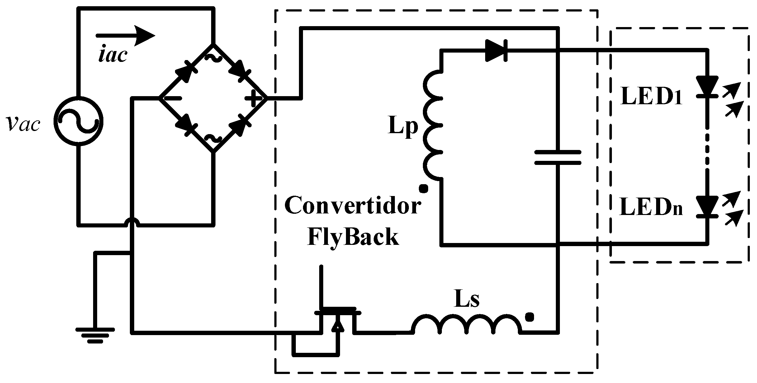
The proposed converter is a re-arranged variation of the flyback converter; placing the secondary of the flyback in parallel with the load and this arrangement is connected in series with the primary side and the rectified voltage source. This configuration allows part of the energy from the source to pass directly to the load, and another part to be processed by the rearranged flyback converter, thus increasing the efficiency of the entire system. To analyze the proposed circuit, a low frequency averaged analysis (LFAA) was carried out, which resulted in an equivalent circuit that was very easy to evaluate and thus determine its behavior and design method. As the flyback converter is an isolated topology, it is possible to use some other of the aforementioned methods, such as ripple ports, to be able to eliminate low-frequency ripple current in the load. This paper is organized as follows:
Section 2 presents and explains the operation and mathematical analysis of the converter.
Section 3 focuses on converter design and simulation in Spice.
Section 4 shows the results obtained, and finally, in
Section 5, the main conclusions of this document are presented.
2. Mathematical Analysis of the Proposed Circuit
The interface between the AC power supply and an LED load is called online LED driver, the driver should have a power factor greater than 0.9 according to the U.S. Energy Star program [
2]. The LED drivers must also comply with the current harmonics level specified in IEC 61000-3-2 Class C [
3]. Therefore, a Power Factor Converter (PFC) should be used to meet the usual requirements for an LED power supply. In
Figure 1 the proposed topology is shown. The converter consists of a variation of the flyback converter in which the secondary stage is connected in parallel with the LED lamp and these in turn in series with the primary stage.
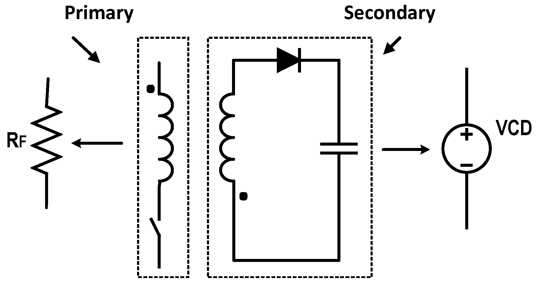
In order to carry out the analysis of the rearranged flyback converter, a low-frequency average analysis (LFAA) was used; This is used to know in a general way if a topology complies with the corresponding regulations, knowing its efficiency, and evaluating its feasibility of implementation. The LFAA model the behavior of the flyback converter at the frequency line. At this frequency and due to the discontinues conduction mode (DCM) of the flyback converter, the primary side can be represented as a loss-free resistance (
RF), this resistance represents the average power delivered to the primary side of the flyback converter (
PFi), the energy “consumed” by this resistance is transferred to the secondary side of the flyback converter that is modeled as a direct current voltage source (
VF), as shown in
Figure 2.
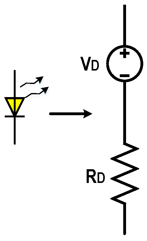
On the LED side, it can be modeled as a series direct DC voltage source with a resistor, as shown in
Figure 3.
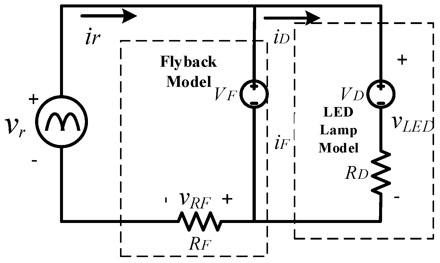
Figure 4 shows the equivalent low-frequency scheme corresponding to the circuit proposed in
Figure 1. Where:
vr is the rectified Voltage,
ir is the rectified Current,
VF is the average voltage in the secondary of the flyback converter,
RF Loss-free resistance representing the primary of the flyback converter,
VD representing the LED threshold voltage of the LED model,
RD is the resistance of the LED model.
The loss free resistance is evaluated with the following expression:
where
IRrms is the RMS value of
ir. 2.1. Analysis of the Power Factor (PF) and the Current Total Harmonic Distortion (THDi) Using LAAA
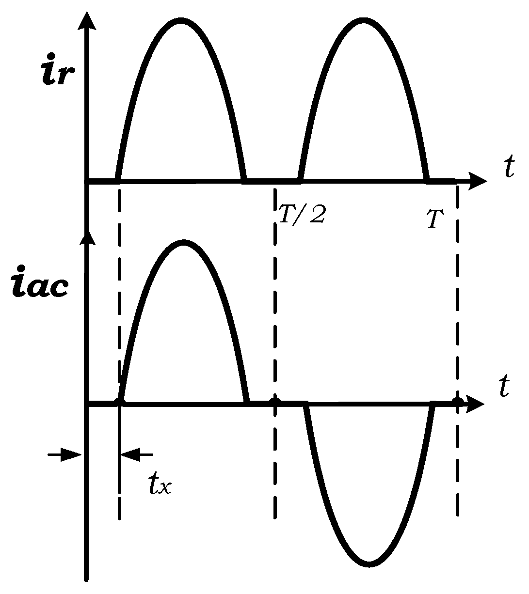
In
Figure 4, it is observed that the LED is powered by the voltage source
VF, it is interesting to obtain the expression of
ir. applying Kirchhoff’s voltage law to the scheme we obtain:
Additionally, the following observations were made:
The topology is reductive, so it is always true that VF < Vr, where Vr is the peak voltage of vr(t), as shown in (4).
There will be current flow through
RF if
vr >
VF, when
vr <
VF the current
ir(
t) = 0, as
Vr approaches
VF there will be very long death times. Therefore, the
ir waveform will be the same as
iac at
T/
2 as shown in
Figure 5.
where
tx is a constant that represents the dead time, which is given by:
where
m =
VF/
Vr is the gain of the proposed converter,
ω is the angular frequency and
f is the line frequency.
In order to calculate the
PF and
THDi in the proposed converter, it is necessary to know the harmonics of the input current waveform (
iac), shown in (6). For this,
tx can be used in the integration limits of the calculation of the Fourier coefficients of
iac in (7) and verify if the topology meets the requirements of IEC61000-3-2 class C.
The waveform being analyzed (
iac) is an odd function, therefore there are only odd harmonics. The
THDi is obtained from (8), where
I1 is the fundamental component that is defined in (9), and
In is the amplitude of the
n-th harmonic that is defined in (10).
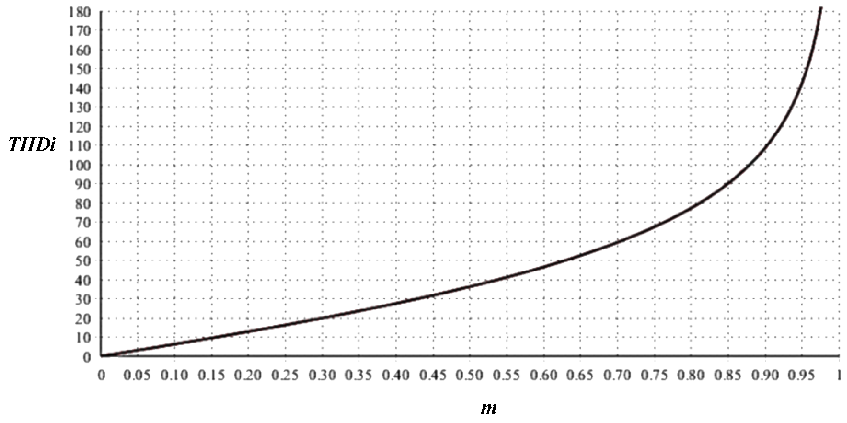
Returning to (8) and assuming the main voltage is sinusoidal the PF is obtained by:
Figure 6 shows the plot of (8), assuming
THDi ≤ 32%., it can be seen that the gain
m can vary from 0 to 0.46. If
m > 0.46 the
THDi will be very high and the power factor
PF very low.
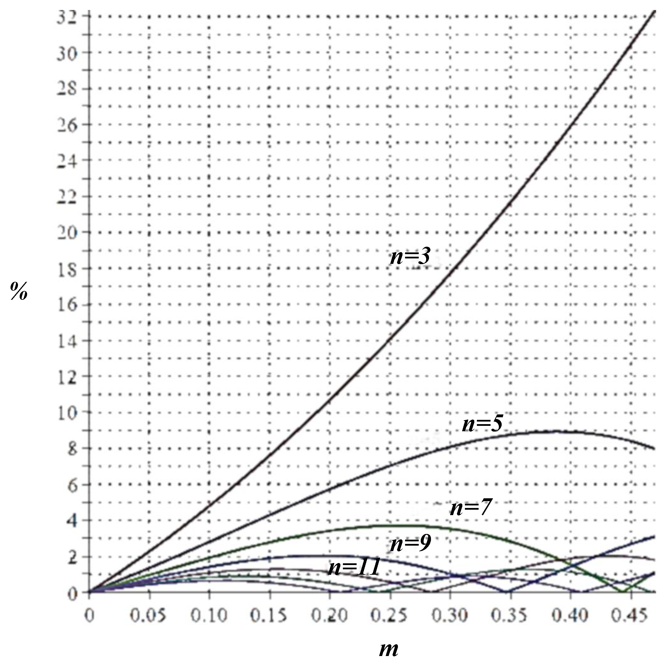
Regarding the requirements of the IEC61000-3-2,
Figure 7 shows the curves for the odd harmonics from
n = 3 to
n = 15, it is observed that the topology is limited in a range of 0 <
m < 0.41.
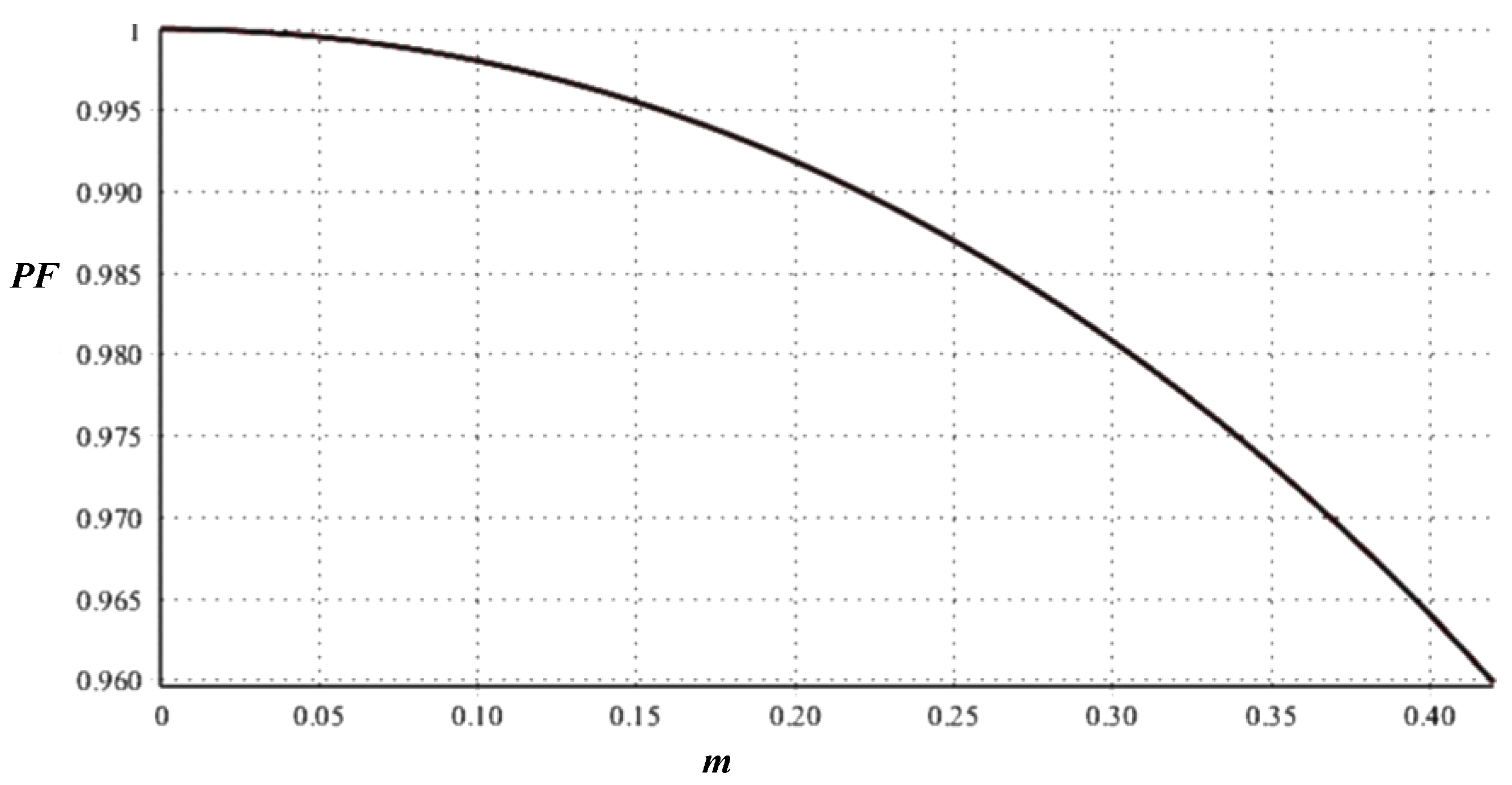
From
Figure 8, where (11) is plotted, it can be seen that the topology meets the requirements of a
PF > 90 without a problem in a range of 0 <
m < 0.41.
From this section it is concluded that the proposed topology complies with all applicable standards in the range of 0 < m < 0.41.
2.2. Analysis of the Power Flow in the Converter
In order to analyze the power flow in the proposed converter the following concepts are defined in
Table 1.
Figure 9 shows the power flow diagram of a conventional flyback compared with the proposed rearranged flyback. In this diagram, it is easier to understand the operation of the proposed converter, in which it is observed as part of the input power
Pi is supplied directly to the load, while the other fraction is processed by the
PFi flyback converter. Therefore, the total efficiency concerning the conventional flyback will be improved.
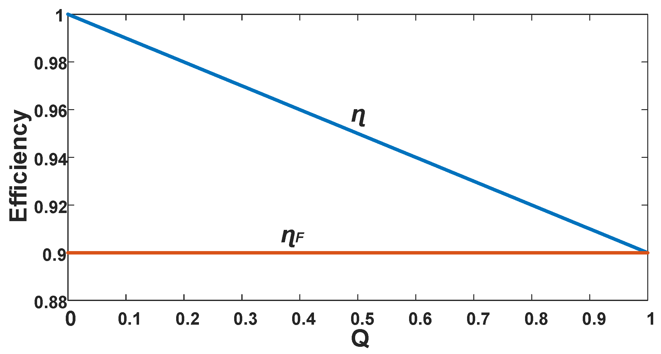
The percentage of power processed by the flyback is called the constant Q. The range of Q must be 0 < Q < 1, if Q is greater than 1 there is no point in implementing the topology since instead of having benefits, low efficiency and greater electrical size would be obtained concerning an isolated basic flyback.
According to
Figure 9 the total efficiency η of the converter will be:
This equation was plotted in
Figure 10 assuming an arbitrary value for the flyback efficiency
ηF = 0.9. As can be seen in this figure, regardless of the Q value, the efficiency of the proposed converter will always be greater than the efficiency of a conventional flyback. Total efficiency will increase as the flyback converter processes less energy.
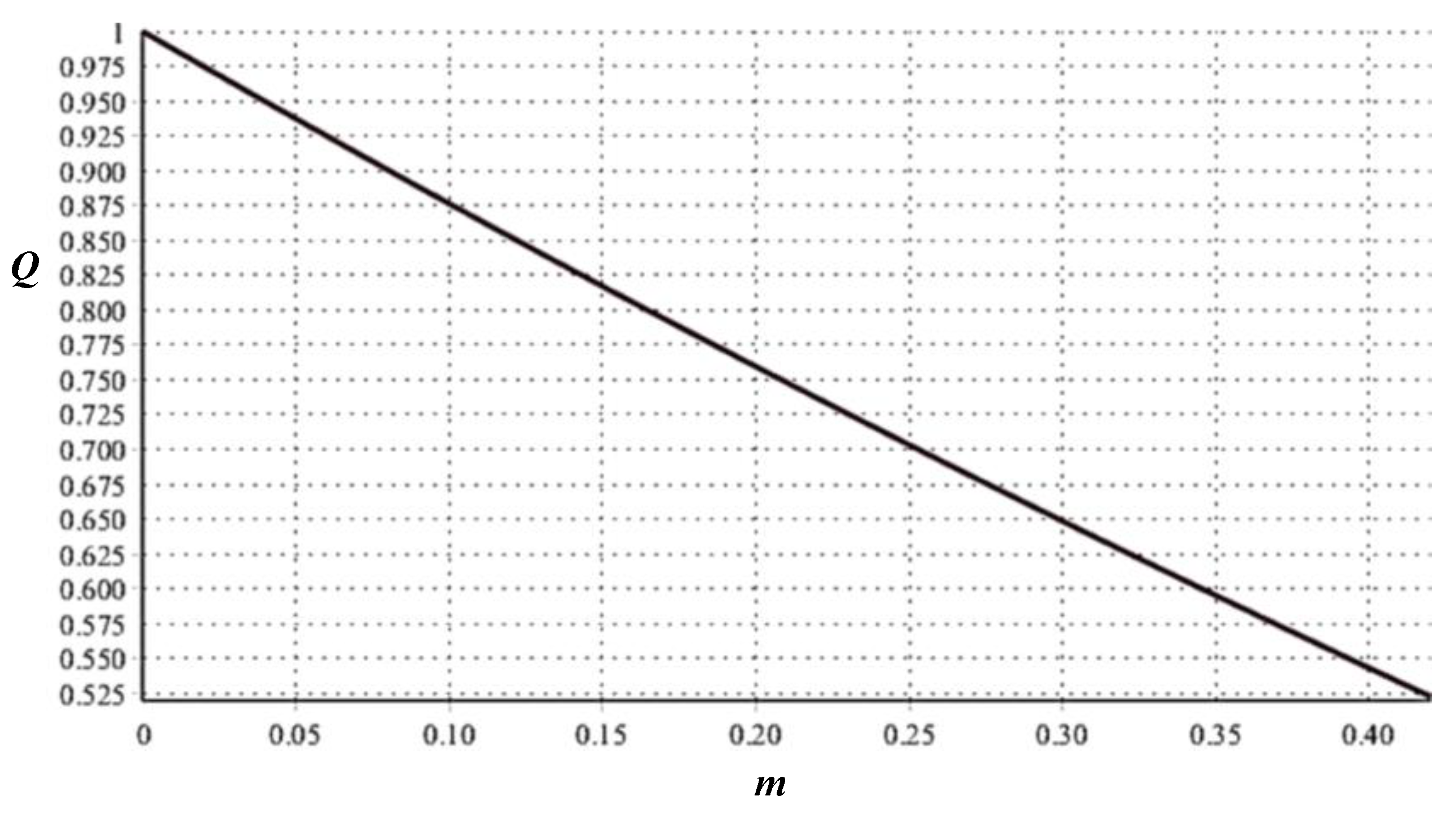
Substituting (3) and (4) in the expressions of
Table 1 with the definition of
m:
In
Figure 11, the graph (23) is obtained, in which it is observed that when
m increases,
Q decreases; this is favorable since the flyback by processing fewer power benefits the total efficiency of the system.
3. Design of the Rearranged Flyback
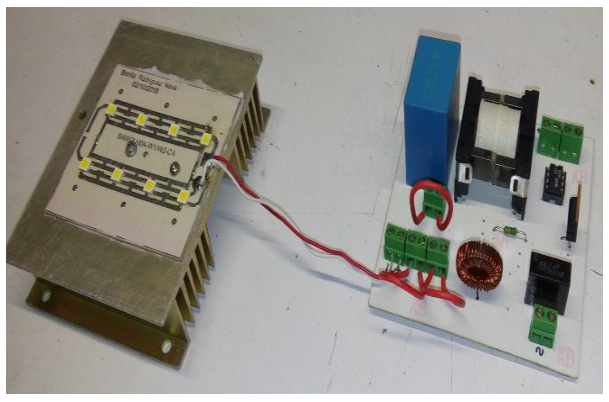
For the implementation of the rearranged flyback converter circuit, LEDs were purchased from the manufacturer Seoul Semiconductor with part number SAW0LH0A. An array of 8 LEDs was made in parallel, which is shown in Figure 14.
The resulting specifications of the LED array are shown in
Table 2, which will be used to simulate at low frequency.
In order to calculate the components of the converter, some design parameters must be proposed, which are shown in
Table 3, among them it is worth noting that the flyback dead time is defined in DCM for AC-DC converters [
16]. With the values of
Table 3, and the equations previously developed, the necessary values for the implementation of the converter are shown in
Table 4.
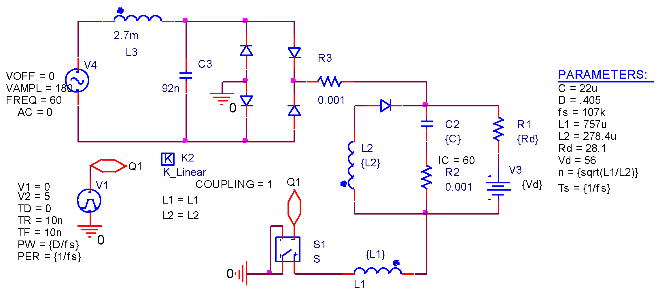
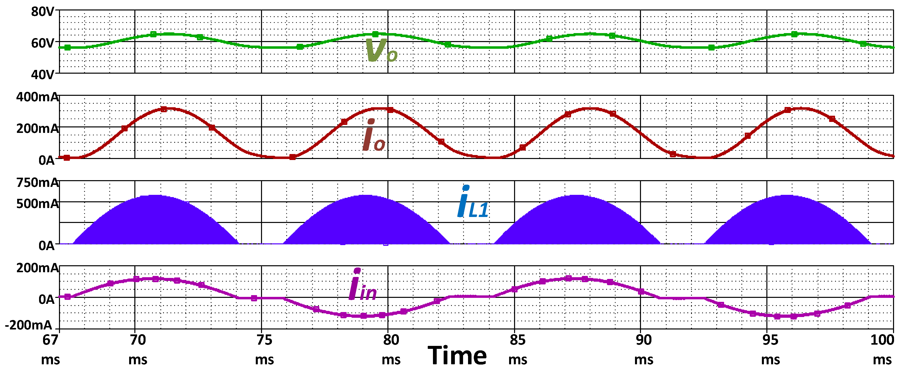
In order to evaluate the proposed circuit before the implementation, a simulation of the circuit was made in Spice. In
Figure 12, The schematic is shown, and the results of the simulation are shown in
Figure 13.
4. Experimental Results
A laboratory prototype has been built to carry out experimental tests and evaluate the performance of the proposed converter. an IR2106 driver and a MOSFET IRF840 were used. The prototype for experimental tests is shown in
Figure 14.
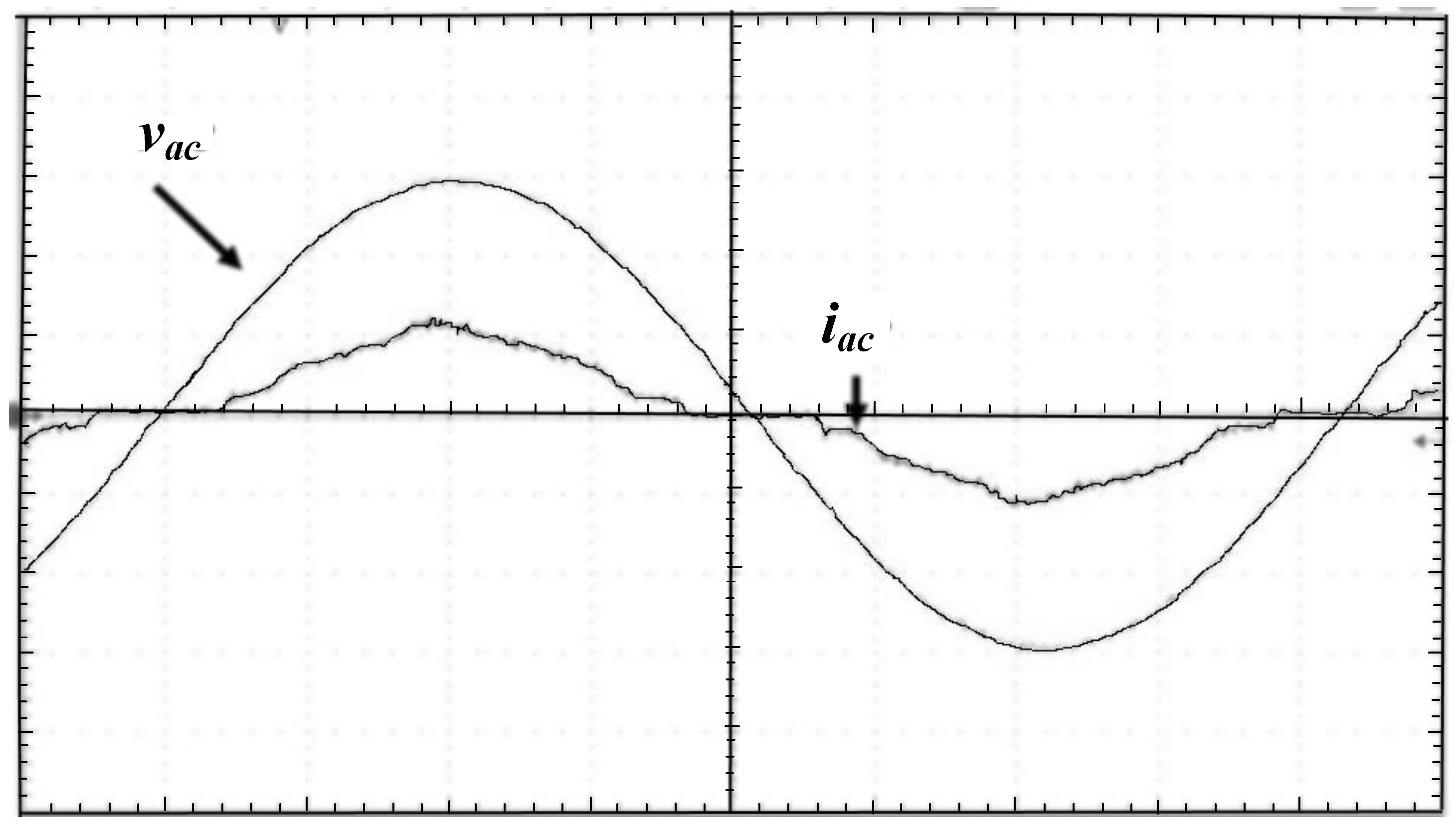
Figure 15 shows the main line current and voltage waveforms. As can be seen in this Figure the current waveform shows the death time
tx predicted by the LFAA and this waveform is similar to the theoretical waveform shown in
Figure 5.
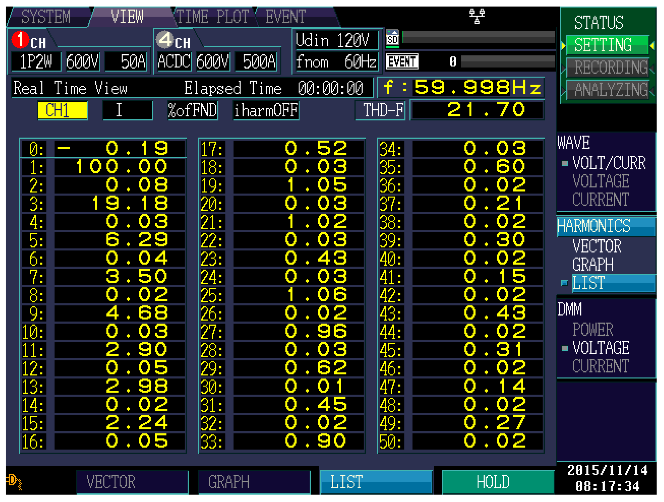
The
THDi of the input waveforms of
Figure 15 was measured with the HIOKI model PW3198 power quality analyzer, which is shown in
Figure 16, which shows that the
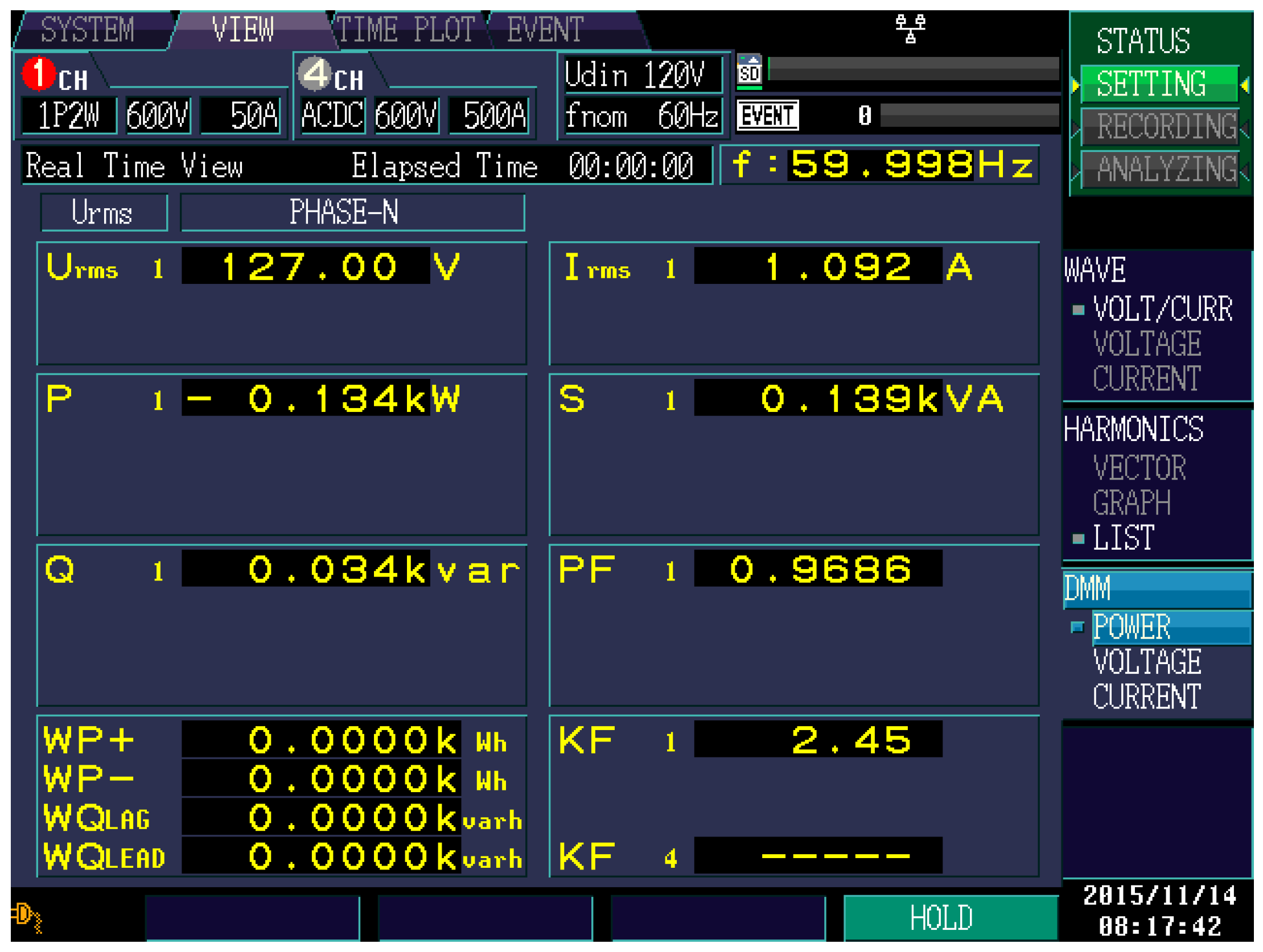
THDi is close to 21.7% and the harmonics are within the requirements of the EN 61000-3-2 class C standard. As for the
PF obtained in experimental tests with the energy quality meter, it is shown to be 0.9686 in
Figure 17.
The instantaneous voltage of the LED lamp obtained in experimental tests is shown in
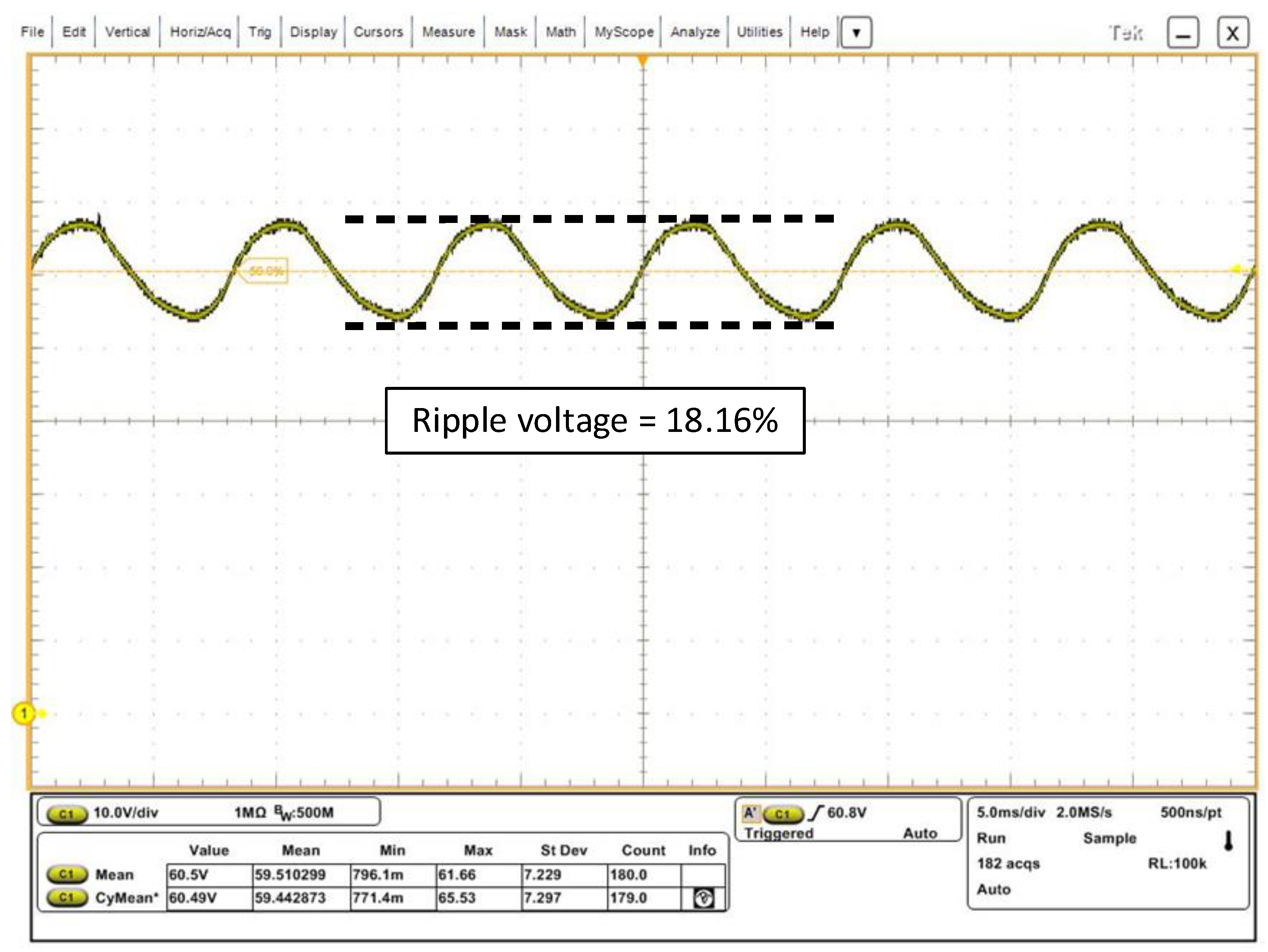
Figure 18. The average voltage applied to the LED was
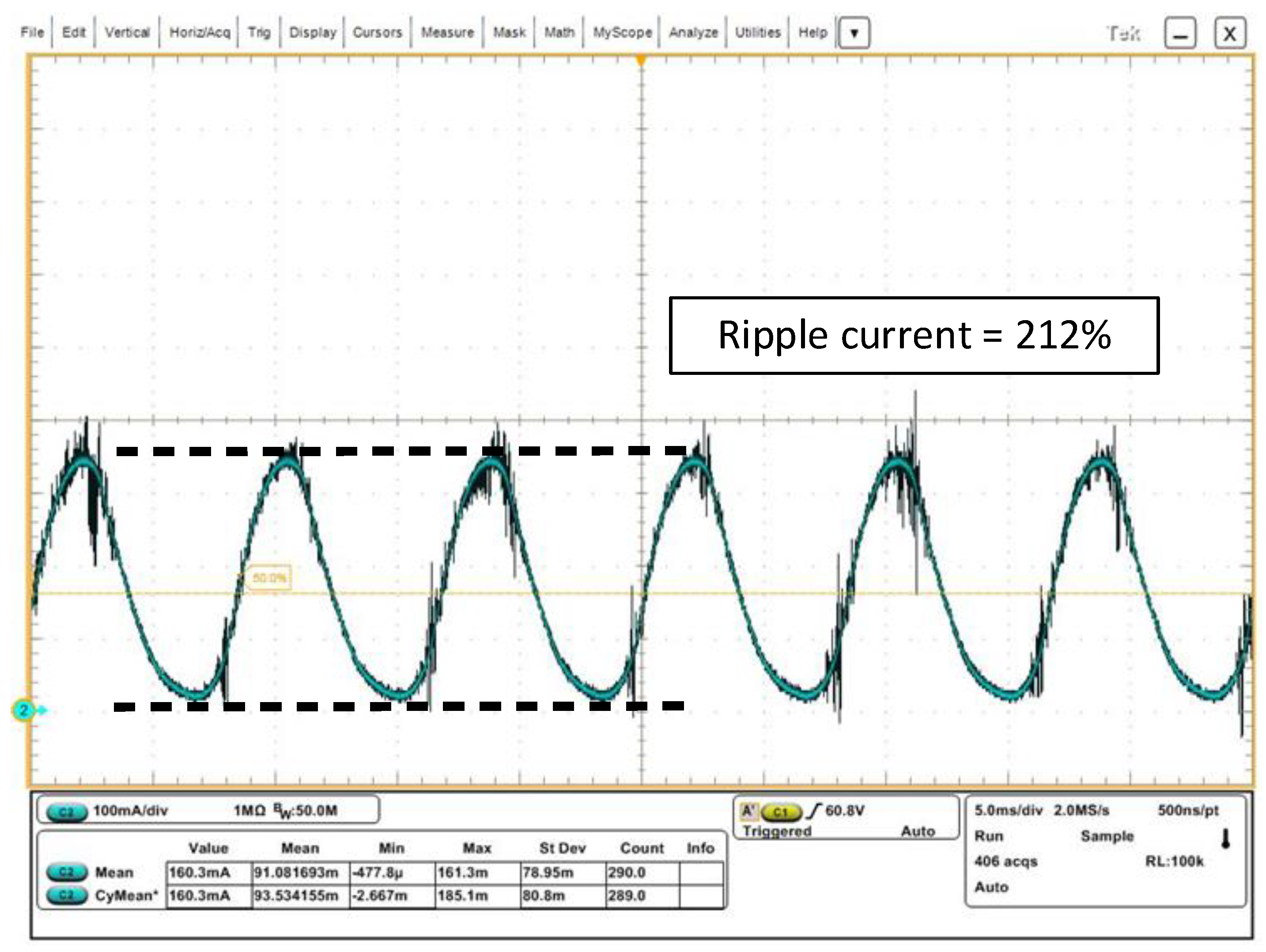
VLED = 60.5, the same of the specifications, the voltage ripple obtained was 18.16%. The instantaneous current of the LED lamp obtained in experimental tests is shown in
Figure 19. The average current applied to the LED was
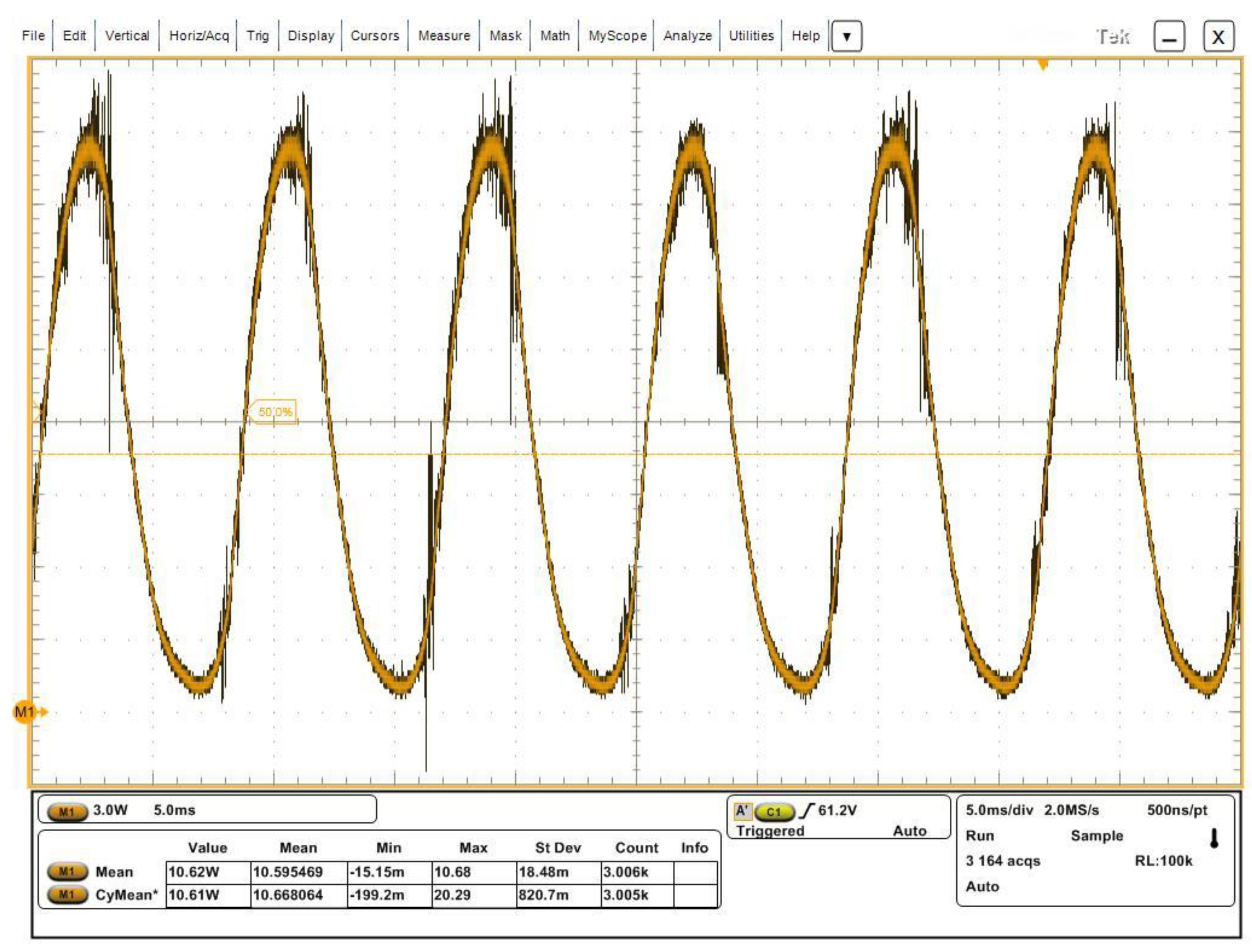
ILED = 160.3 mA, the current ripple obtained was 212%. Finally, in
Figure 20 the instantaneous output power in the LED is shown. which shows an average power of
Po = 10.62 W.
Finally,
Table 5 and
Table 6 summarize what was obtained in the implementation of the topology and the percentages of error obtained, and as expected, there are parameters such as in the case of
THDi with a higher percentage of error, this is since losses of the elements used were not considered, in addition to this the construction of the prototype, to mention the manual manufacture of the transformer, which can considerably affect the performance of the entire system.
It should be noted that the flyback only processes 63% of the input power.
Finally,
Table 7 shows a small comparison with a couple of similar power topologies. It can be seen that the topology has a good efficiency and power factor compared to the other two topologies, and even less energy stored in the capacitor is reported, which translates into a physically smaller capacitor. However, it has a greater current ripple.
5. Conclusions
Through this document, a new converter has been evaluated which is based on a variant of the flyback converter and is used as a power supply in solid-state lighting systems.
The proposed converter consists of a rearrangement of the components of the conventional flyback, the secondary is placed in parallel with the LED load and this set is in turn placed in series with the primary and the voltage source.
The primary advantage of this converter is the partial processing of energy, which goes beyond the principle of reduced redundant energy processing (R
2P
2) [
16], one part of the energy is directly delivered to the load and the other part is processed by the converter. Since in this rearrangement the flyback converter processed less energy, the stress in the components is lower than in a conventional flyback. As well, this operation allows the efficiency of the proposed converter to always will be greater than the conventional flyback converter. The main disadvantages are the converter have not magnetic isolation, it is a reductive topology and the power factor depends on the gain
m of the converter.
The mathematical analysis of the topology of the retrofitted flyback converter was performed and it was shown that it complies with the requirements established by the IEC61000-3-2 class C standard and the FIDE directives in an interval of 0 < m < 0.41, with a THDi = 21.7% and a PF = 0.9686.
In order to validate the mathematical calculations, a 10 W prototype was built. Experimental results show the rearranged flyback processed only 63% of the input power and the other 37% flows directly to the load.

 ,
, 


