
A Versatile, Voltage-Pulse Based Read and Programming Circuit for Multi-Level RRAM Cells

 , , , , , and
Abstract
:1. Introduction
2. RRAM Technology
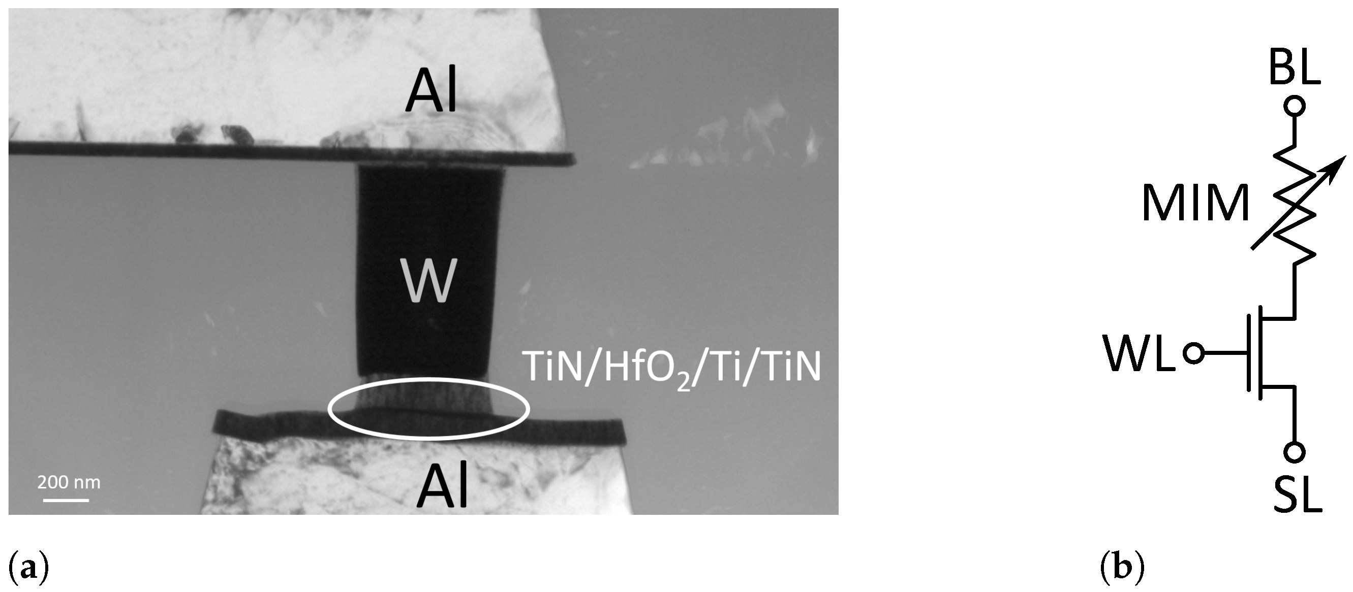
2.1. 1T1R RRAM Cells
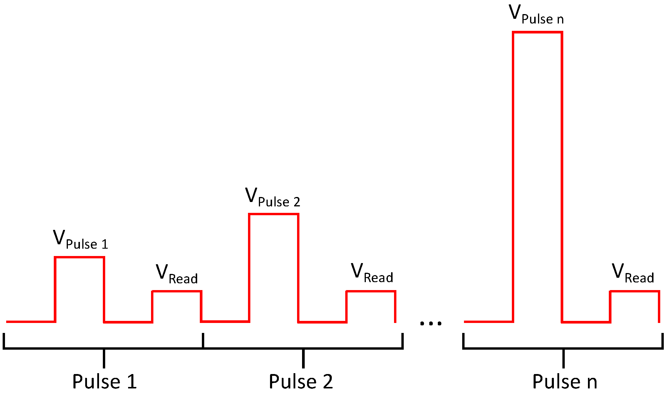
2.2. Programming Algorithm
2.3. Cell Variability
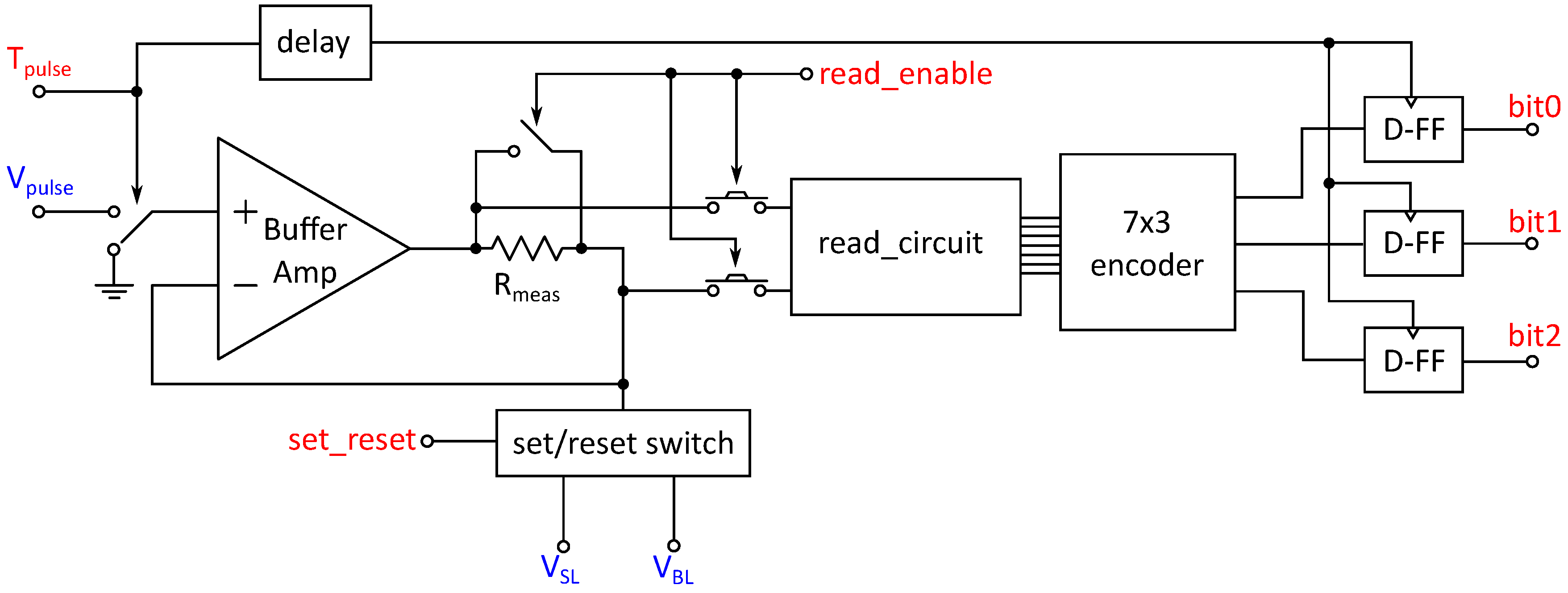
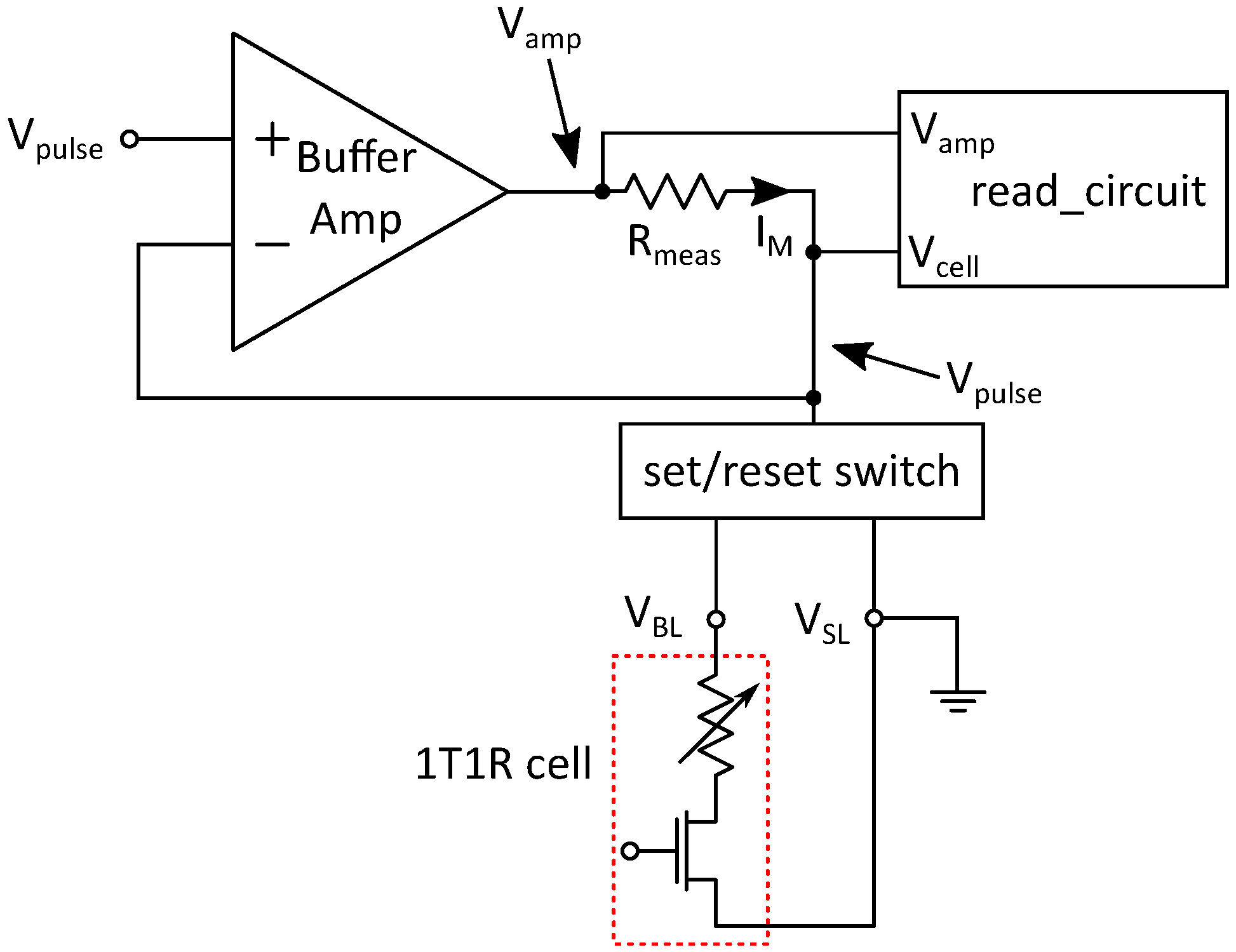
3. Circuit Overview
3.1. Programming Operation
3.2. Read Operation
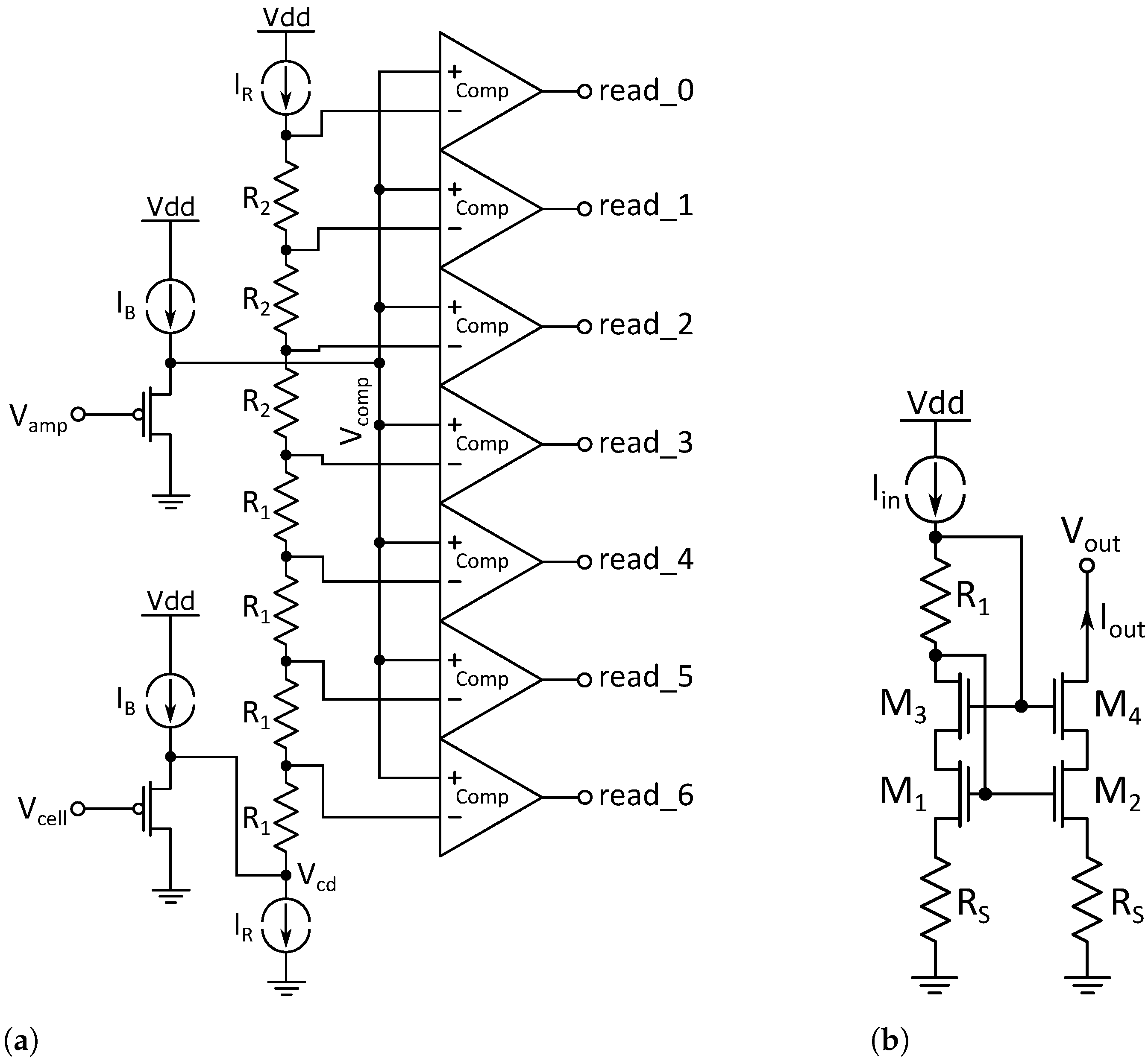
4. Read Circuit
- Provide a high input impedance to decouple the read circuit from the measurement resistor. This is necessary to prevent current flow into the read circuit
- Shift the relatively low input voltage of away from ground supply, therefore providing a voltage headroom for the current source
5. Simulation and Measurement Results
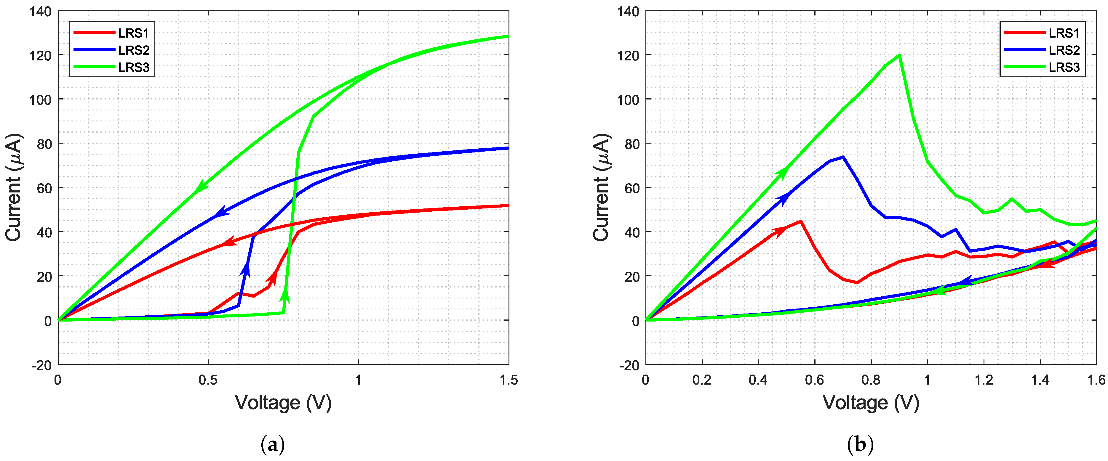
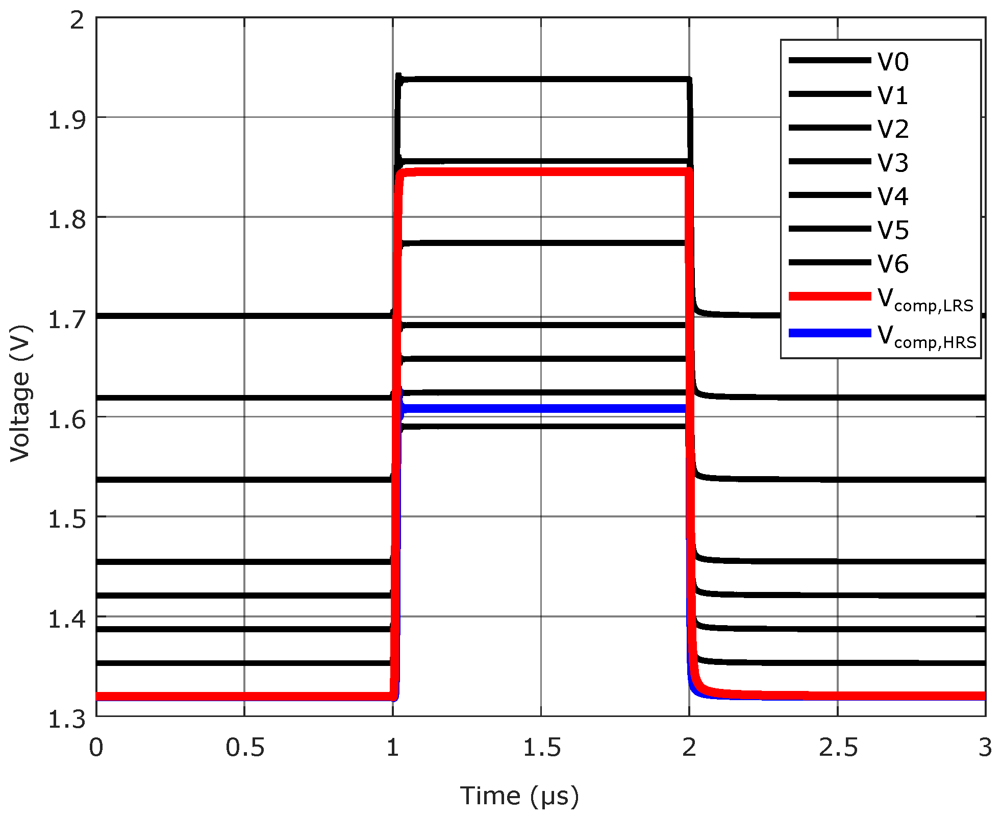
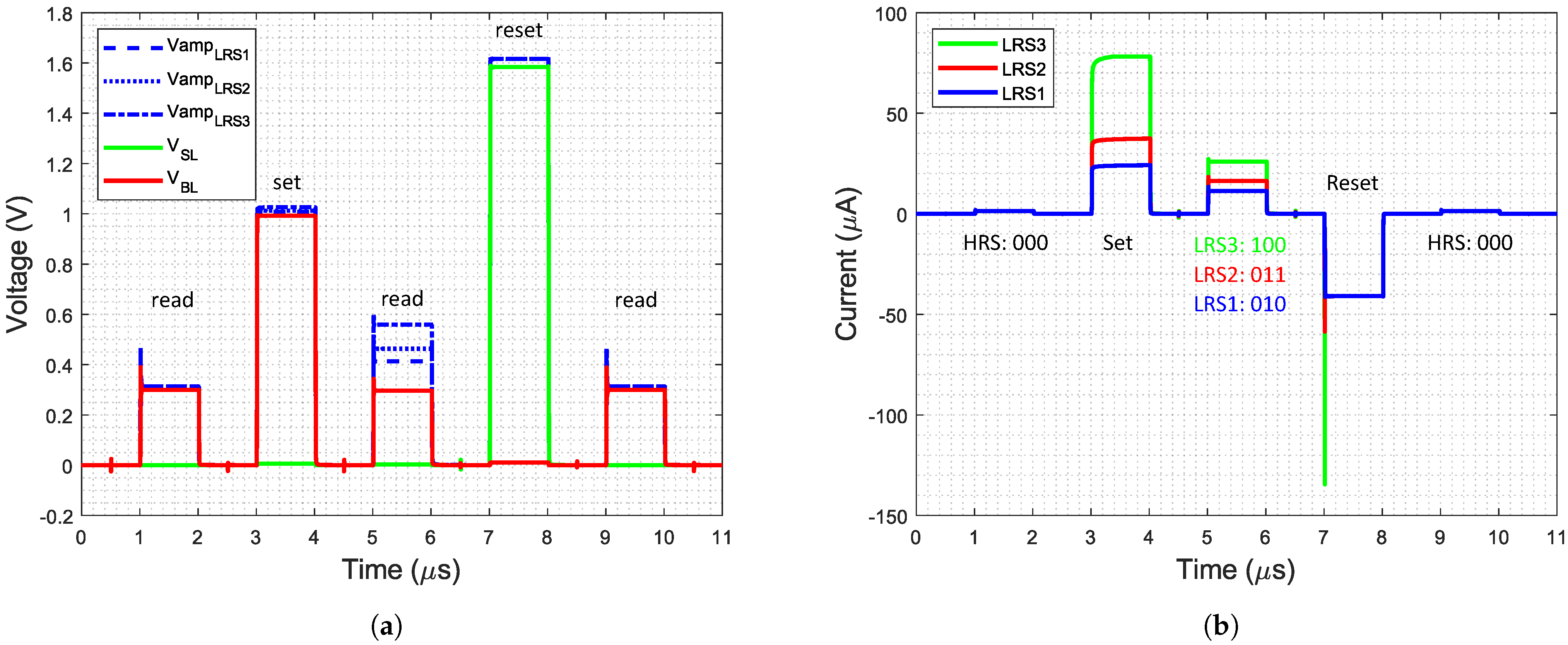
5.1. Simulation Results
- LRS3: 100
- LRS2: 011
- LRS1: 010
- HRS: 000
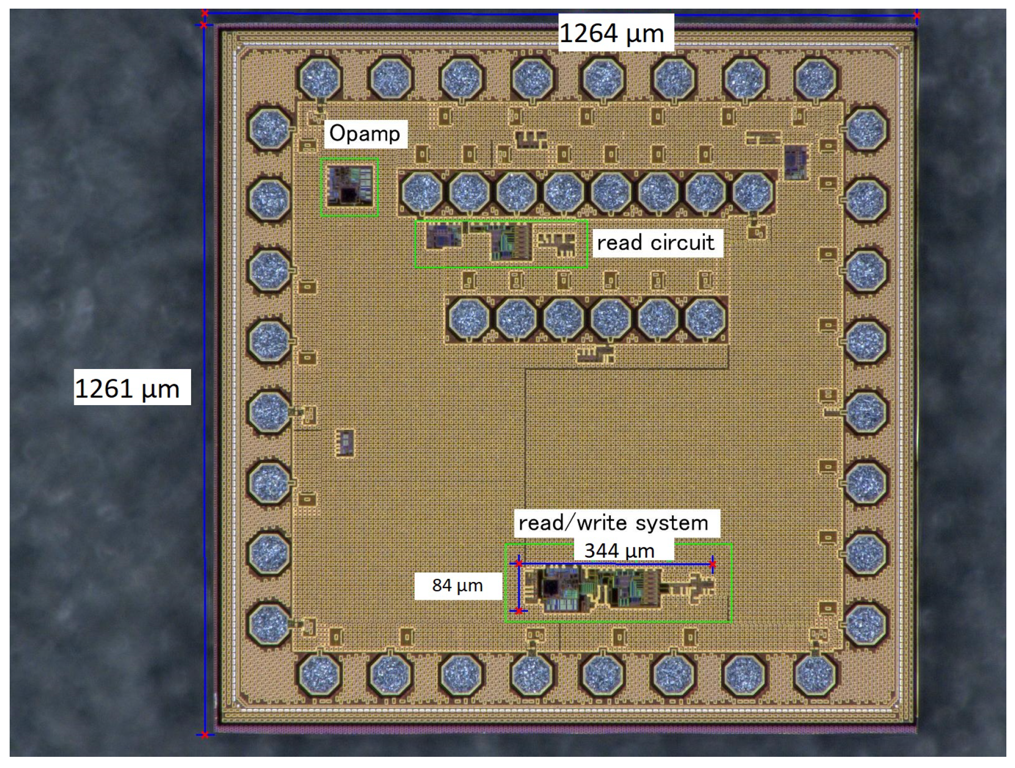
5.2. Measurement Results Read Circuit
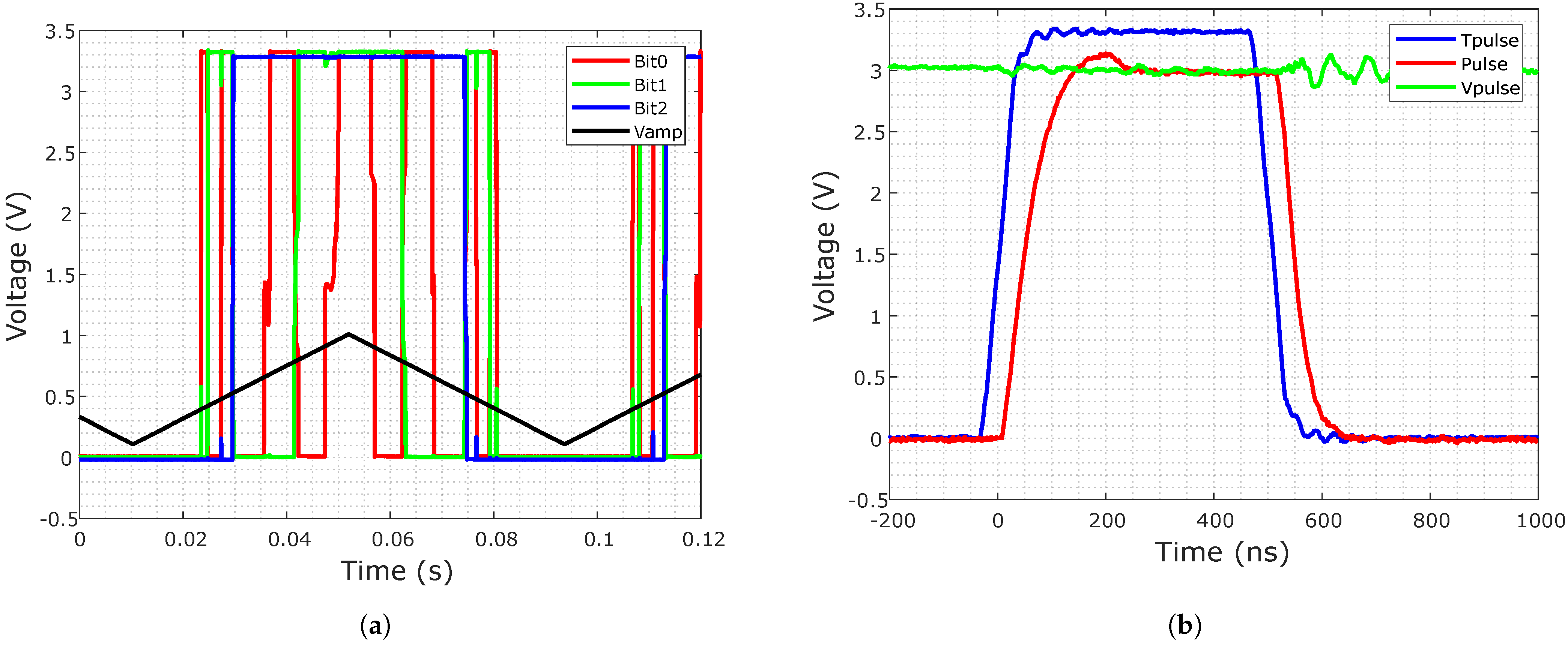
5.3. Measurement Results System
5.3.1. Programming System
5.3.2. Read System
6. Discussion and Comparison with Other Read and Programming Circuits
7. Conclusions
Author Contributions
Funding
Institutional Review Board Statement
Informed Consent Statement
Data Availability Statement
Acknowledgments
Conflicts of Interest
Abbreviations
| RRAM | Resistive Random Access Memory |
| PUF | Physical unclonable function |
| SRAM | Static Random Access Memory |
| FF | Flip Flop |
| NVM | Non-volatile Memory |
| AI | Artificial Intelligence |
| ML | Machine Learning |
| BL | Bitline |
| SL | Sourceline |
| WL | Wordline |
| MIM | Metal-Insulator-Metal |
| 1T1R | One-Transistor/One-Resistor |
| BEOL | Back end of line |
| SEM | Scanning electron microscope |
| HRS | High resistive state |
| LRS | Low resistive state |
| ISPVA | Incremental Step Pulse and Verify Algorithm |
| LSB | Least significant bit |
| MSB | Most significant bit |
References
- Covi, E.; Lin, Y.; Wang, W.; Stecconi, T.; Milo, V.; Bricalli, A.; Ambrosi, E.; Pedretti, G.; Tseng, T.; Ielmini, D. A Volatile RRAM Synapse for Neuromorphic Computing. In Proceedings of the 2019 26th IEEE International Conference on Electronics, Circuits and Systems (ICECS), Genoa, Italy, 27–29 November 2019; pp. 903–906. [Google Scholar]
- Kawahara, A.; Azuma, R.; Ikeda, Y.; Kawai, K.; Katoh, Y.; Hayakawa, Y.; Tsuji, K.; Yoneda, S.; Himeno, A.; Shimakawa, K.; et al. An 8 Mb Multi-Layered Cross-Point ReRAM Macro With 443 MB/s Write Throughput. IEEE J. Solid-State Circuits 2013, 48, 178–185. [Google Scholar] [CrossRef]
- Kim, K.H.; Gaba, S.; Wheeler, D.; Cruz-Albrecht, J.M.; Hussain, T.; Srinivasa, N.; Lu, W. A Functional Hybrid Memristor Crossbar-Array/CMOS System for Data Storage and Neuromorphic Applications. Nano Lett. 2012, 12, 389–395. [Google Scholar] [CrossRef] [PubMed]
- Biglari, M.; Lieske, T.; Fey, D. High-Endurance Bipolar ReRAM-Based Non-Volatile Flip-Flops with Run-Time Tunable Resistive States. In Proceedings of the 14th IEEE/ACM International Symposium on Nanoscale Architectures NANOARCH ’18, Athens, Greece, 17–19 July 2018; Association for Computing Machinery: New York, NY, USA, 2018; pp. 19–24. [Google Scholar] [CrossRef]
- Reuben, J.; Pechmann, S. A Parallel-friendly Majority Gate to Accelerate In-memory Computation. In Proceedings of the 2020 IEEE 31st International Conference on Application-specific Systems, Architectures and Processors (ASAP), Manchester, UK, 6–8 July 2020; pp. 93–100. [Google Scholar]
- Zahoor, F.; Zulkifli, T.Z.A.; Khanday, F.A. Resistive Random Access Memory (RRAM): An Overview of Materials, Switching Mechanism, Performance, Multilevel Cell (mlc) Storage, Modeling, and Applications. Nanoscale Res. Lett. 2020, 15, 90. [Google Scholar] [CrossRef]
- Yu, S.; Chen, P. Emerging Memory Technologies: Recent Trends and Prospects. IEEE Solid-State Circuits Mag. 2016, 8, 43–56. [Google Scholar] [CrossRef]
- Wu, H.; Zhao, M.; Liu, Y.; Yao, P.; Xi, Y.; Li, X.; Wu, W.; Zhang, Q.; Tang, J.; Gao, B.; et al. Reliability Perspective on Neuromorphic Computing Based on Analog RRAM. In Proceedings of the 2019 IEEE International Reliability Physics Symposium (IRPS), Monterey, CA, USA, 31 March–4 April 2019; pp. 1–4. [Google Scholar] [CrossRef]
- Pérez, E.; Maldonado, D.; Acal, C.; Ruiz-Castro, J.; Alonso, F.; Aguilera, A.; Jiménez-Molinos, F.; Wenger, C.; Roldán, J. Analysis of the statistics of device-to-device and cycle-to-cycle variability in TiN/Ti/Al:HfO2/TiN RRAMs. Microelectron. Eng. 2019, 214, 104–109. [Google Scholar] [CrossRef]
- Grossi, A.; Perez, E.; Zambelli, C.; Olivo, P.; Wenger, C. Performance and reliability comparison of 1T-1R RRAM arrays with amorphous and polycrystalline HfO2. In Proceedings of the 2016 Joint International EUROSOI Workshop and International Conference on Ultimate Integration on Silicon (EUROSOI-ULIS), Vienna, Austria, 25–27 January 2016; pp. 80–83. [Google Scholar] [CrossRef] [Green Version]
- Milo, V.; Zambelli, C.; Olivo, P.; Pérez, E.; Mahadevaiah, M.K.; Ossorio, O.G.; Wenger, C.; Ielmini, D. Multilevel HfO2-based RRAM devices for low-power neuromorphic networks. APL Mater. 2019, 7. [Google Scholar] [CrossRef] [Green Version]
- Pérez, E.; Grossi, A.; Zambelli, C.; Olivo, P.; Roelofs, R.; Wenger, C. Reduction of the Cell-to-Cell Variability in Hf1-xAlxOyBased RRAM Arrays by Using Program Algorithms. IEEE Electron Device Lett. 2017, 38, 175–178. [Google Scholar] [CrossRef] [Green Version]
- Crupi, F.; Filice, F.; Grossi, A.; Zambelli, C.; Olivo, P.; Perez, E.; Wenger, C. Implications of the Incremental Pulse and Verify Algorithm on the Forming and Switching Distributions in RERAM Arrays. IEEE Trans. Device Mater. Reliab. 2016, 16, 413–418. [Google Scholar] [CrossRef] [Green Version]
- Pérez, E.; Grossi, A.; Zambelli, C.; Olivo, P.; Wenger, C. Impact of the Incremental Programming Algorithm on the Filament Conduction in HfO2-Based RRAM Arrays. IEEE J. Electron Devices Soc. 2017, 5, 64–68. [Google Scholar] [CrossRef]
- Pérez, E.; Zambelli, C.; Kalishettyhalli Mahadevaiah, M.; Olivo, P.; Wenger, C. Towards Reliable Multi-Level Operation in RRAM Arrays: Improving Post-Algorithm Stability and Assessing Endurance/Data Retention. IEEE J. Electron Devices Soc. 2019, 7, 740–747. [Google Scholar] [CrossRef]
- Yu, S. Overview of resistive switching memory (RRAM) switching mechanism and device modeling. In Proceedings of the 2014 IEEE International Symposium on Circuits and Systems (ISCAS), Melbourne, VIC, Australia, 1–5 June 2014; pp. 2017–2020. [Google Scholar] [CrossRef]
- Ciocoveanu, R.; Bahr, A.; Krautschneider, W. Design of a Rail-to-Rail Folded Cascode Amplifier with Transconductance Feedback Circuit. In Proceedings of the ITC Open Conference, Amersfoort, The Netherlands, 14–16 September 2016; pp. 21–24. [Google Scholar]
- Gray, P. Analysis and Design of Analog Integrated Circuits, 5th ed.; Wiley Global Education: Hoboken, NJ, USA, 2009. [Google Scholar]
- Pérez, E.; Ossorio, O.G.; Dueñas, S.; Castán, H.; García, H.; Wenger, C. Programming Pulse Width Assessment for Reliable and Low-Energy Endurance Performance in Al:HfO2-Based RRAM Arrays. Electronics 2020, 9, 864. [Google Scholar] [CrossRef]
- Reuben, J.; Fey, D.; Wenger, C. A Modeling Methodology for Resistive RAM Based on Stanford-PKU Model With Extended Multilevel Capability. IEEE Trans. Nanotechnol. 2019, 18, 647–656. [Google Scholar] [CrossRef] [Green Version]
- Hossam, H.; Mamdouh, G.; Hussein, H.H.; El-Dessouky, M.; Mostafa, H. A New Read Circuit for Multi-Bit Memristor-Based Memories based on Time to Digital Sensing Circuit. In Proceedings of the 2018 IEEE 61st International Midwest Symposium on Circuits and Systems (MWSCAS), Windsor, ON, Canada, 5–8 August 2018; pp. 1114–1117. [Google Scholar] [CrossRef]
- Manem, H.; Rose, G.S. A read-monitored write circuit for 1T1M multi-level memristor memories. In Proceedings of the 2011 IEEE International Symposium of Circuits and Systems (ISCAS), Rio de Janeiro, Brazil, 15–18 May 2011; pp. 2938–2941. [Google Scholar] [CrossRef]
- Elshamy, M.; Mostafa, H.; Ghallab, Y.H.; Said, M.S. A Novel Nondestructive Read/Write Circuit for Memristor-Based Memory Arrays. IEEE Trans. Very Large Scale Integr. (VLSI) Syst. 2015, 23, 2648–2656. [Google Scholar] [CrossRef]


| State | Resistance | WL Voltage |
|---|---|---|
| LRS1 | ≈16 kΩ | 1 |
| LRS2 | ≈ kΩ | |
| LRS3 | ≈ kΩ | |
| HRS | ≈200 kΩ |
| Name | Type | In/Out | Function |
|---|---|---|---|
| Tpulse | digital | Input | length of voltage pulse |
| Vpulse | analog | Input | height of voltage pulse |
| read_enable | digital | Input | read or programming operation |
| set_reset | digital | Input | polarity of voltage pulse |
| VSL | analog | Output | SL voltage signal |
| VBL | analog | Output | BL voltage signal |
| bit<0:2> | digital | Output | read values |
| Corresponding | Output | |
|---|---|---|
| <380 | > | 000 |
| 380 | 001 | |
| 420 | 25 | 010 |
| 475 | 011 | |
| 530 | 13 | 100 |
| 660 | 101 | |
| 780 | 110 | |
| ≥930 | ≤ | 111 |
| Measurement Resistance | Read Values | State |
|---|---|---|
| 96% 110; 4% 101 | LRS3 | |
| 100% 100 | LRS2 | |
| 16 | 84% 010; 16% 011 | LRS1 |
| 200 | 100% 000 | HRS |
Publisher’s Note: MDPI stays neutral with regard to jurisdictional claims in published maps and institutional affiliations. |
© 2021 by the authors. Licensee MDPI, Basel, Switzerland. This article is an open access article distributed under the terms and conditions of the Creative Commons Attribution (CC BY) license (http://creativecommons.org/licenses/by/4.0/).
Share and Cite
Pechmann, S.; Mai, T.; Völkel, M.; Mahadevaiah, M.K.; Perez, E.; Perez-Bosch Quesada, E.; Reichenbach, M.; Wenger, C.; Hagelauer, A. A Versatile, Voltage-Pulse Based Read and Programming Circuit for Multi-Level RRAM Cells. Electronics 2021, 10, 530. https://doi.org/10.3390/electronics10050530
Pechmann S, Mai T, Völkel M, Mahadevaiah MK, Perez E, Perez-Bosch Quesada E, Reichenbach M, Wenger C, Hagelauer A. A Versatile, Voltage-Pulse Based Read and Programming Circuit for Multi-Level RRAM Cells. Electronics. 2021; 10(5):530. https://doi.org/10.3390/electronics10050530
Chicago/Turabian StylePechmann, Stefan, Timo Mai, Matthias Völkel, Mamathamba K. Mahadevaiah, Eduardo Perez, Emilio Perez-Bosch Quesada, Marc Reichenbach, Christian Wenger, and Amelie Hagelauer. 2021. "A Versatile, Voltage-Pulse Based Read and Programming Circuit for Multi-Level RRAM Cells" Electronics 10, no. 5: 530. https://doi.org/10.3390/electronics10050530