Article

Impact of the Chaotic Synchronization’s Stability on the Performance of QCPSK Communication System

Institute of Radioelectronics, Riga Technical University, Kalku St. 1, LV-1050 Riga, Latvia
*
Author to whom correspondence should be addressed.
Electronics 2021, 10(6), 640; https://doi.org/10.3390/electronics10060640
Submission received: 22 January 2021 / Revised: 28 February 2021 / Accepted: 1 March 2021 / Published: 10 March 2021
(This article belongs to the Special Issue Recent Advances in Chaotic Systems and Their Security Applications)

Abstract

:
The current work presents a study of the implementation of a quadrature chaos phase-shift keying communication system (QCPSK) based on the employment of different chaos oscillators. The research takes two directions, with one being the study of the chaos synchronization’s noise immunity for several chaos oscillators that are the potential core blocks of the QCPSK system. The correlation coefficient over time is used to estimate the synchronization noise immunity. The second direction is the estimation of the QCPSK system’s baseband model performance in the AWGN propagation channel using the bit error ratio (BER) as the estimation method for several chaos oscillators employed as the core of the QCPSK system’s model.

1. Introduction

The reason for the increasing interest in the employment of chaos phenomenon as a building block in the design of communication systems is supported by the characteristics of the chaos-based communication systems: non-periodic, noise-like signal waveform, wide frequency bandwidth, and sensitive dependence on initial conditions. These properties allow the additional physical layer of security for the information transfer. In the ongoing digital transformation of the world in such directions as the internet of things (IoT) and wireless sensor networks (WSNs), there is a demand for highly efficient, wideband, secure communication, that could be ensured by the use of chaos-based data transmission systems [1,2]. Having grasped the benefits of the employment of chaos in data communication, the various chaos-based modulation schemes were introduced and studied. These modulation schemes are generally divided into two broad groups: noncoherent modulation schemes and coherent modulation schemes.
In the case of coherent modulation schemes, the in-phase synchronization between the receiver and the transmitter must be sustained. The modulation schemes that refer to this group are chaos-shift keying (CSK) [3,4], quadrature chaos shift-keying (QCSK) [5], chaos-based code division multiple access (CDMA) [6]. In the CSK system, two or more chaos generators with different parameters are located in the transmitter. The information is transmitted utilizing switching between signals from the corresponding chaos generators. The QCSK system adds the employment of the orthogonal signals, increasing the rate of band usage.
In the case of noncoherent modulation schemes, in-phase synchronization is not required. The modulation schemes of this group are chaos on-off keying (COOK) [7], differential chaos-shift keying (DCSK) [8], frequency-modulated differential chaos-shift keying (FM-DCSK) [9]. In COOK, the chaos generator is turned on when the “1” bit is transmitted and off when the “0” bit is transmitted. The receiver then estimates the energy of the received signal. For the received “1” bit, the energy of the signal is notably higher. The DCSK modulation scheme uses two consecutive parts of the chaotic signal in one symbol transmission, the first part is a reference signal, and the second part bears the information. The FM-DCSK utilizes frequency modulation performed by chaotic signals.
Complementing many possible chaos modulations, several approaches in implementing chaos signal generators exist. The first type of chaotic generators are known as chaotic maps, also referred to as chaotic functions [10,11]. Another approach for generating chaotic signals is to employ chaotic systems defined with a set of differential equations. Chaotic systems of such type are implemented using either analog circuit arithmetic [12] or analog circuit state variables [13,14,15].
In [16], we proposed a model of quadrature chaos phase-shift keying-based communication system (QCPSK) employing chaos oscillators (defined by state variable differential equations). The current paper further investigates the proposed system using some approaches for the study developed in Reference [17].
The paper is organized in the following way: the model of the communication system based on chaos phase-shift keying and the quadrature transceiver is presented in Section 2. Section 3 describes the chaos oscillators employed in the research of the presented communication system. In Section 4, the first step of the research is to study the synchronization properties of the proposed chaos oscillators using simulation, hardware experiments, and analysis of the results acquired in this step. Section 5 describes the second step of the research, which is focused on investigating the performance of the proposed communication system with the employment of the chaos oscillators studied in the first step. The performance is estimated using the baseband model of the communication system in the AWGN propagation channel. Section 5 also includes the analysis of the results acquired in the second step of the research. The final section presents conclusions.

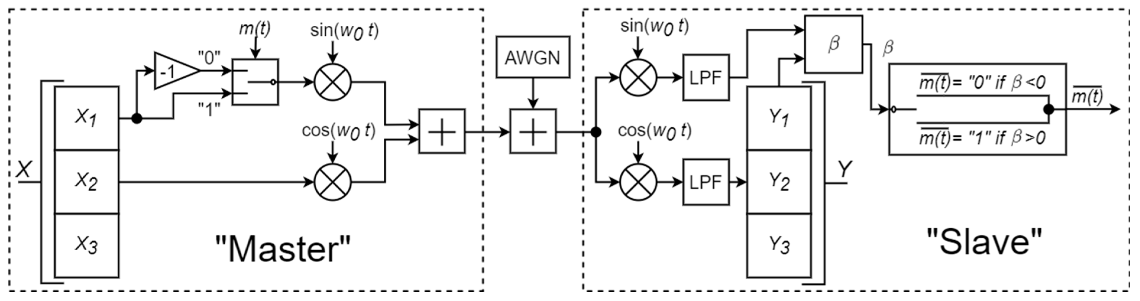
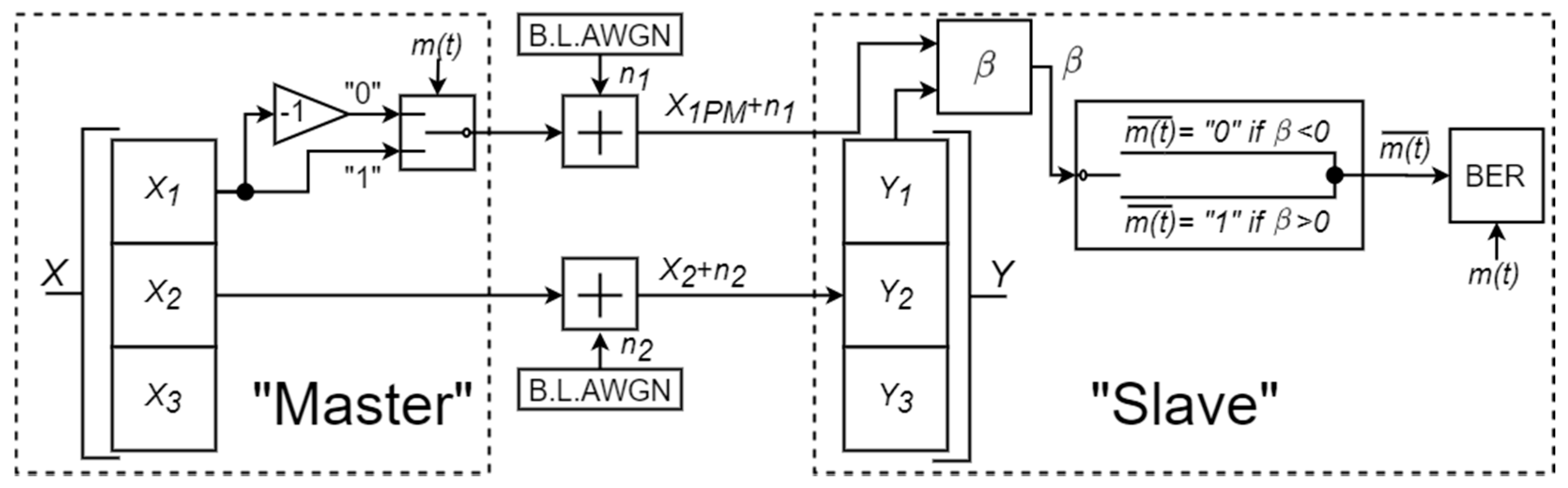
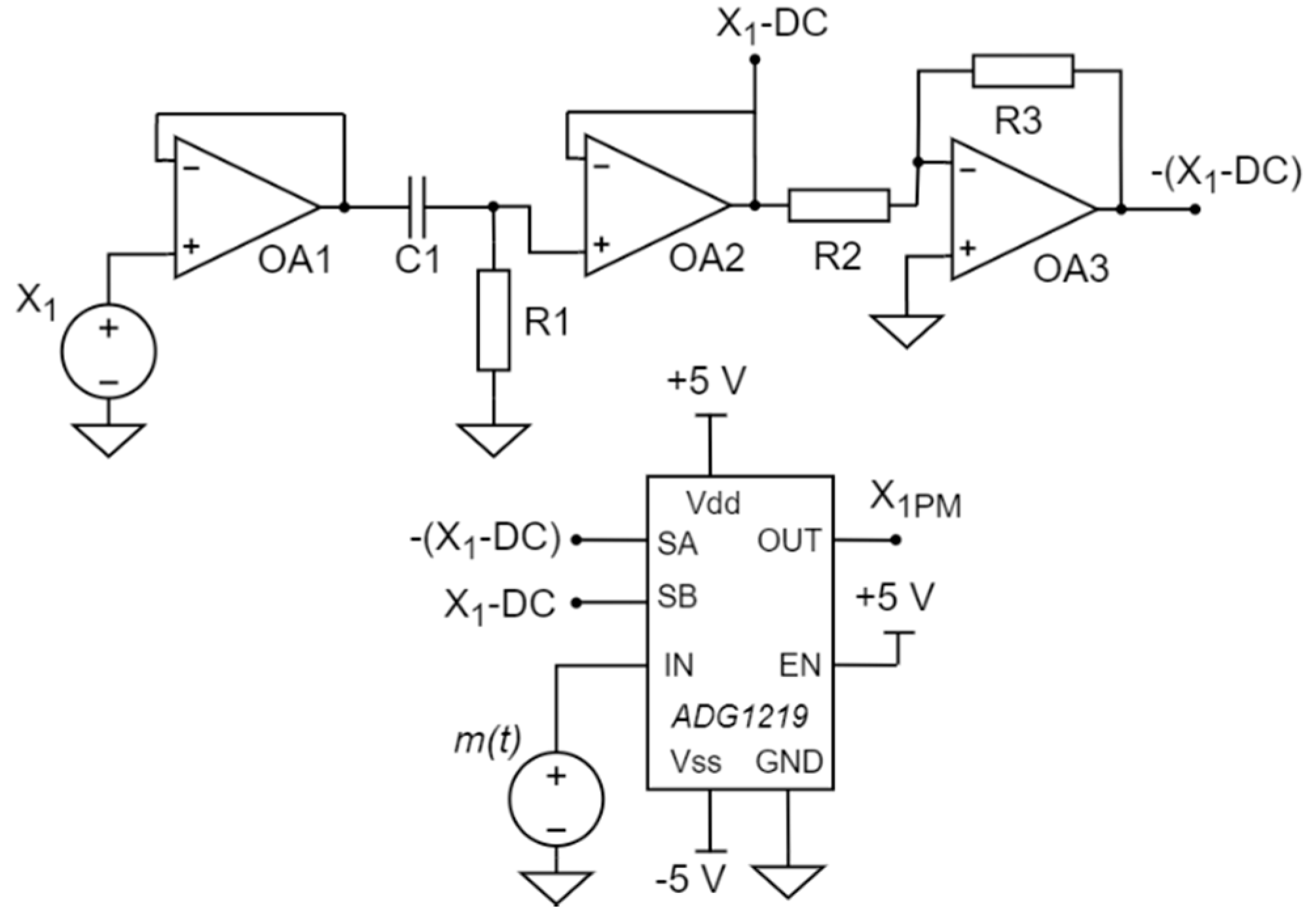
2. Communication System Based on Quadrature Chaos Phase-Shift Keying

The current section presents the model of a communication system first proposed with the description of the applied elements and their functions in [16]. The block diagram for the communication system under investigation is shown in Figure 1.
X and Y in Figure 1 represent two systems exhibiting chaotic behavior. These systems are described by the state variables, which are X 1 , X 2 , X 3 for the X system, and Y 1 , Y 2 , Y 3 for the Y system. The state variables of chaotic systems are also referred to as chaotic signals. The “master” device utilizes X 1 and X 2 state variables for data transmission. The state variable X 1 is used to encode the binary message m ( t ) , ensured by a corresponding data-driven switch. When the “1” bit is transmitted, the output of the switch is equal to X 1 , and when the “0” bit is transmitted, the output of the switch is equal to X 1 . In the “master” device synchronization and the encoded message signals are then fed into the quadrature modulator. The X 2 , which is used as a synchronization signal between chaotic systems X and Y , is the in-phase component (commonly referred to as “I”) of the baseband signal. It is up-converted to the passband by multiplying it with a cosine waveform having a frequency w 0 , which is regarded as the carrier frequency. In turn, the message signal is the quadrature component (commonly referred to as “Q”) of the baseband signal and it is up-converted to the passband by multiplying it with a sine waveform having the same carrier frequency. The master device transmits the modulated harmonic signal, which is the sum of up-converted I and Q components. The environment between the transmitter and the receiver is modeled as a direct additive white Gaussian noise (AWGN) channel [16].
In the “slave” device, the quadrature demodulator and the low-pass filters (LFP) are used to down-convert the received passband signal from the carrier frequency and separate synchronization signal carried by the “I” component, and encoded message signal carried by the “Q” component of the baseband signal. The synchronization signal X 2 substitutes Y 2 , thereby causing Y 1 repeat behavior of X 1 and Y 3 , repeat behavior of X 3 . This type of chaotic synchronization is called “substitution-based chaos synchronization”. Studies [10,17,18,19] demonstrated that replacing a single state variable of a chaotic system Y with a similar state variable from a similar chaotic system X results in Y system, following the behavior of X . In this configuration, the X system acts as “master” and Y system acts as “slave”. Moreover, Section 4 introduces differential equitation systems of investigated chaotic oscillators showing how state variables impact each other. Differential equitation systems of “master” and “slave” systems are absolutely the same, except substitution.
Y To decode the received message signal, a time-windowed correlation coefficient β is calculated for a pair of Y 1 and the received encoded message signal (which is either X 1 or X 1 ). The correlation coefficient β is greater than 0 when X 1 is received, and less than 0 when X 1 is received. At perfect conditions β = 1 for X 1 , and β = −1 for X 1 , β = 1 means Y 1 and X 1 are precisely identical, while β = −1 shows that Y 1 and X 1 are precisely opposite because of X 1 . β = 0 indicates the absence of correlation between the two signals. The final block interprets the results of the correlation coefficient as binary “1” if β > 0 and “0” if β < 0 , thereby acquiring the decoded message signal m ( t ) ¯ [16].

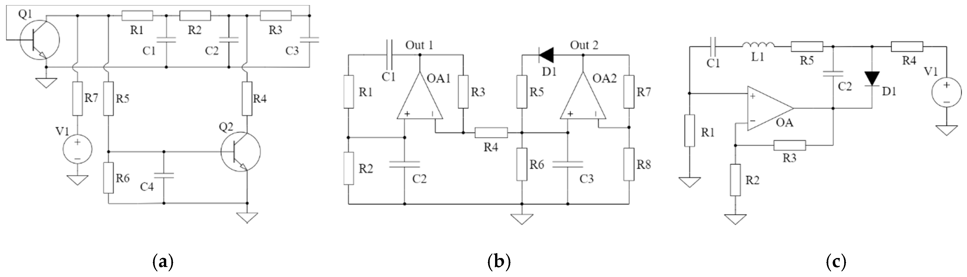
3. Chaos Oscillators

As shown in the previous section, the most important components of the proposed communication system defining its performance are chaotic oscillators. The chaos oscillators selected for this research were: the “Simple Two-Transistor Single-Supply Resistor-Capacitor Chaotic Oscillator” [15], “Simple RC chaotic oscillator” [14] and “A simple chaotic oscillator for educational purposes” [13] (also referred to as “Vilnius chaotic oscillator” [17]). For the sake of simplicity, the following denotation is used for the mentioned chaos oscillators throughout this paper: “RC1 chaos oscillator”, “RC2 chaos oscillator” and “Vilnius chaos oscillator.” This section further describes each of the mentioned chaos oscillators starting with the RC1. The circuit diagram of every mentioned chaos oscillator is shown in Figure 2.
From Figure 2a, the mathematical model of the RC1 oscillator is represented with a set of differential equations, Equation (1) [15,16], where the state variables are the voltages across the capacitors C 1 C 4 .
R B C d v C 1 d t = v C 1 ( 1 + R B R A R B R 5 R A ( 2 R 5 + R A ) ) + v C 1 + R B R 5 2 R 5 + R A ( V 1 R A i C 1 + v B E 2 R 5 ) , R B C d v C 2 d t = 2 v C 2 + v C 1 + v B E 1 i C 4 R B , R B C d v B E 1 d t = v B E 1 + v C 2 i B 1 R B , ( 2 R 5 + R A ) C 4 d v B E 2 d t = v B E 2 ( 2 + ( 2 R 5 + R A ) R 6 ) + v C 1 + V 1 i C 1 R A i B 2 ( 2 R 5 + R A ) ,
where R A = R 1 = R 7 = 5.6 kΩ; R B = R 2 = R 3 = 10 kΩ; R 4 = 15 kΩ; R 5 = 33 kΩ; R 6 = 47 kΩ; C = C 1 = C 2 = C 3 = 1 nF; C 4 = 330 pF; v C 1 —voltage across the capacitor C 1 ; v C 2 —voltage across the capacitor C 2 ; i C 1 —current through the capacitor C 1 ; i C 4 —current through the capacitor C 4 ; v B E 1 —base-emitter voltage of the 2N3904 transistor Q 1 (is equal to the voltage across the capacitor C 3 ); v B E 2 —base-emitter voltage of the 2N3904 transistor Q 2 (is equal to the voltage across the capacitor C 4 ); V 1 —5.8 V power supply voltage [15,16].
The circuit diagram of the RC2 chaos oscillator, shown in Figure 2b, could be described by the differential equations presented in Equation (2) [14]. From Equations (2)–(4), it is seen that the state variables are the voltages across the capacitors C 1 , C 2 , C 3 , as well as the output voltages of the operational amplifiers O A 1 and O A 2 .
x ˙ = x + ( k 1 1 ) y ( k 1 1 ) z , y ˙ = x + ( k 1 2 ) y ( k 1 1 ) z , z ˙ = y k 1 ( k 1 + α ) z + β ( z 1 ) H ( z 1 ) .
The coefficients of the differential equations for this chaos oscillator are defined from the Figure 2b circuit parameters, summarized in [14]:
v C 1 v * = x , v C 2 v * = y , v C 3 v * = z , v * = v 0 ( k 2 1 ) , d v d t = v ˙ , R R 6 = α , R R 8 = β .
For the circuit in Figure 2b, two additional equations describing the outputs of the operational amplifiers O A 1 and O A 2 are provided as follows:
v o u t 1 = [ k 1 y ( k 1 1 ) z ] v * , v o u t 2 = k 2 z v * .
In Equations (2)–(4), v C 1 —voltage across the capacitor C 1 ; v C 2 —voltage across the capacitor C 2 ; v C 3 —voltage across the capacitor C 3 ; v 0 —voltage across the 1N4148 diode D 1 ; v o u t 1 —TL082 operational amplifier O A 1 output voltage; v o u t 2 —TL082 operational amplifier O A 2 output voltage; k 1 O A 1 gain; k 2 O A 2 gain; R = R 1 = R 2 = 11 kΩ; R 3 = 9.1 kΩ; R 4 = 2 kΩ; R 5 = R 7 = 2.7 kΩ; R 6 = 1.1 kΩ; R 8 = 780 Ω; H —Heaviside step function [14].
The circuit diagram of the Vilnius chaos oscillator is shown in Figure 2c with the mathematical model described by a system of differential equations in Equation (5) [13,17], defining the state variables for the Vilnius chaos oscillator as voltages across the capacitors C 1 and C 2 , and a current through the inductor L 1 .
C 1 d v C 1 d t = i L 1 , L 1 d i L 1 d t = ( k 1 ) R i L 1 v C 1 v C 2 , C 2 d v C 2 d t = i 0 + i L 1 i D ,
where C 1 = 1 nF; C 2 = 150 pF; L 1 = 1 mH; R = R 1 = 1 kΩ; R 2 = R 3 = 10 kΩ; R 4 = 20 kΩ; R 5 = 2.9 Ω; v C —voltage across the capacitor C 1 ; v C 2 —voltage across the capacitor C 2 ; i L —current through the inductor L 1 ; i D —current through the 1N4148 diode D 1 ; i 0 —current through the resistor R 4 ; k —is a gain of the TL082 operational amplifier O A [17]. In Figure 2c, V 1 = 3 V; k = 2.

4. Study of the Properties of Chaos Oscillators

The current section describes the first step in the investigation of the proposed communication system’s performance with the employment of selected chaos oscillators. The first step is the study of noise immunity of chaos oscillator’s synchronization. The importance of this step is approved by the fact that the model of the communication system in Figure 1 is based on the synchronization of two chaotic systems, and the noise immunity of the chaotic synchronization will directly affect the performance of the entire system. This section considers the model of the experiment, complemented with simulation and hardware implementations. The block diagram of the experimental study is depicted in Figure 3.
The experimental model in Figure 3 is resembling the model of the communication system from Figure 1, excluding the message encoder, quadrature modulator-demodulator, and the decision-making device. The model consists of two chaotic systems X (master) and Y (slave). State variables X 2 and Y 2 are used for chaos synchronization, much like in Figure 1. For the study of synchronization’s noise immunity, the environment between the two oscillators is an additive white Gaussian noise channel with a limited frequency bandwidth. The use of band-limited noise signals reflects the influence of low-pass filters (LPF) in Figure 1. This means that the noise signal with the same frequency band as the received chaotic signals will affect the Y system. The frequency bandwidth of the noise signals n 1 and n 2 is equal to the frequency band of the corresponding signals X 1 and X 2 . The noise signal n 2 is added to the synchronization signal X 2 and results in a signal X 2 + n 2 . This signal is applied to the Y system for the Y 2 substitution. The other signal that is being transmitted to the Y system through the noisy environment is X 1 that results in the X 1 + n 1 signal. The simultaneous presence of the noise in the channel for both transmitted signals is assumed as the worst-case scenario. Synchronization of the two systems is estimated using the 100 μs window correlation coefficient β for the signals X 1 + n 1 and Y 1 . The correlation coefficient’s values are in the range from 0 to 1, as only the direct X 1 signal is taken to calculate correlation with Y 1 . The higher value β indicates better synchronization. The window of the correlation coefficient has a fixed time frame like in the model of the communication system in Figure 1. The equation used for calculating the correlation coefficient between the given signals is as follows:
β = m k ( ( X 1 + n 1 ) m k ( X 1 + n 1 ) ¯ ) ( ( Y 1 ) m k ( Y 1 ) ¯ ) m k ( ( X 1 + n 1 ) m k ( X 1 + n 1 ) ¯ ) 2 m k ( ( Y 1 ) m k ( Y 1 ) ¯ ) 2 ,
where β —correlation coefficient; m , k —array indexes.
The n 1 , n 2 noise signal levels are measured in SNR (signal to noise ratio) from 20 dB to 0 dB with a step of 5 dB. The experiment is applied to all of the three previously shown chaos oscillators.

4.1. Simulation-Based Study

This section presents the simulation setup for the experiment shown in Figure 3. The simulation is done using LTspice software for circuit simulation and MATLAB for the required noise signals generation and calculation of the correlation coefficient. The simulation setup for this experiment is shown in Figure 4 using the Vilnius chaos oscillator as an example [17].
Elements in Figure 4 have the following values: R 6 = R 8 = R 9 = 1 kΩ; R 7 = 2 kΩ; R 10 = R 11 = 200 Ω; O A 1 O A 4 are TL082 operational amplifiers. All the operational amplifiers in Figure 4 are supplied with ±3 V. In Figure 4, X 1 is the capacitor’s C 1 M voltage, X 2 is the capacitor’s C 2 M voltage, Y 1 is the capacitor’s C 1 S voltage, Y 2 is the capacitor’s C 2 S voltage. A signal V 2 is the noise n 2 voltage that is added to the capacitor’s C 2 M voltage signal applied to the capacitor C 2 S , like the signal X 2 + n 2 in Figure 3. The signal X 1 + n 1 is obtained summing up the noise signal n 1 with the capacitor’s C 1 M voltage signal [17].
Equation (7) shows the state variable differential equation of the “slave” circuit with C 2 S voltage v C 2 S substituted by C 1 M voltage with noise v C 2 M + V 2 . Equation (7) demonstrates substitution-based chaos synchronization in action: v C 2 S state variable of the “slave” chaos oscillator is replaced with v C 2 M ; assuming V 2 = 0 V. As v L 1 S , v C 1 S , v C 2 S are related, v L 1 S follows the behavior of v L 1 M , and v C 1 S follows v C 1 M —the “slave” oscillator follows the “master” oscillator. Synchronization for chaos oscillators performs exactly as previously described for X and Y chaotic systems in Figure 1. In Equation (7), the influence of noise V 2 on the “slave” chaos oscillator during synchronization can be seen—increasing noise level will deviate the “slave” circuit from following the “master.”
C 1 S d v C 1 S d t = i L 1 S , L 1 S d i L 1 S d t = ( k 1 ) R i L 1 S v C 1 S ( v C 2 M + V 2 ) , C 2 S d ( v C 2 M + V 2 ) d t = i 0 + i L 1 S i D 1 S .
In the case of RC1 chaos oscillator, X 1 is the voltage across the C 1 M capacitor and the Y 1 is the voltage across C 1 S ( C 1 in Figure 2a), X 2 is the voltage of the C 2 M capacitor, and the Y 2 is the voltage of the C 2 S ( C 2 in Figure 2a). In the case of the RC2 chaos oscillator, X 1 is the voltage signal at the output of the operational amplifier O A 2 M and Y 1 is the voltage at the output of the O A 2 S amplifier ( O A 2 in Figure 2b). X 2 is the voltage of the C 2 M and the Y 2 is the voltage of the C 2 S ( C 2 in Figure 2b).

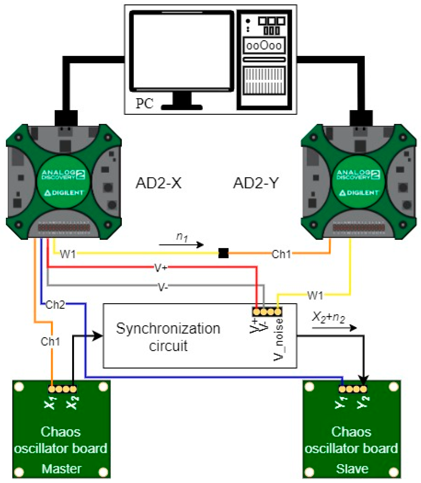
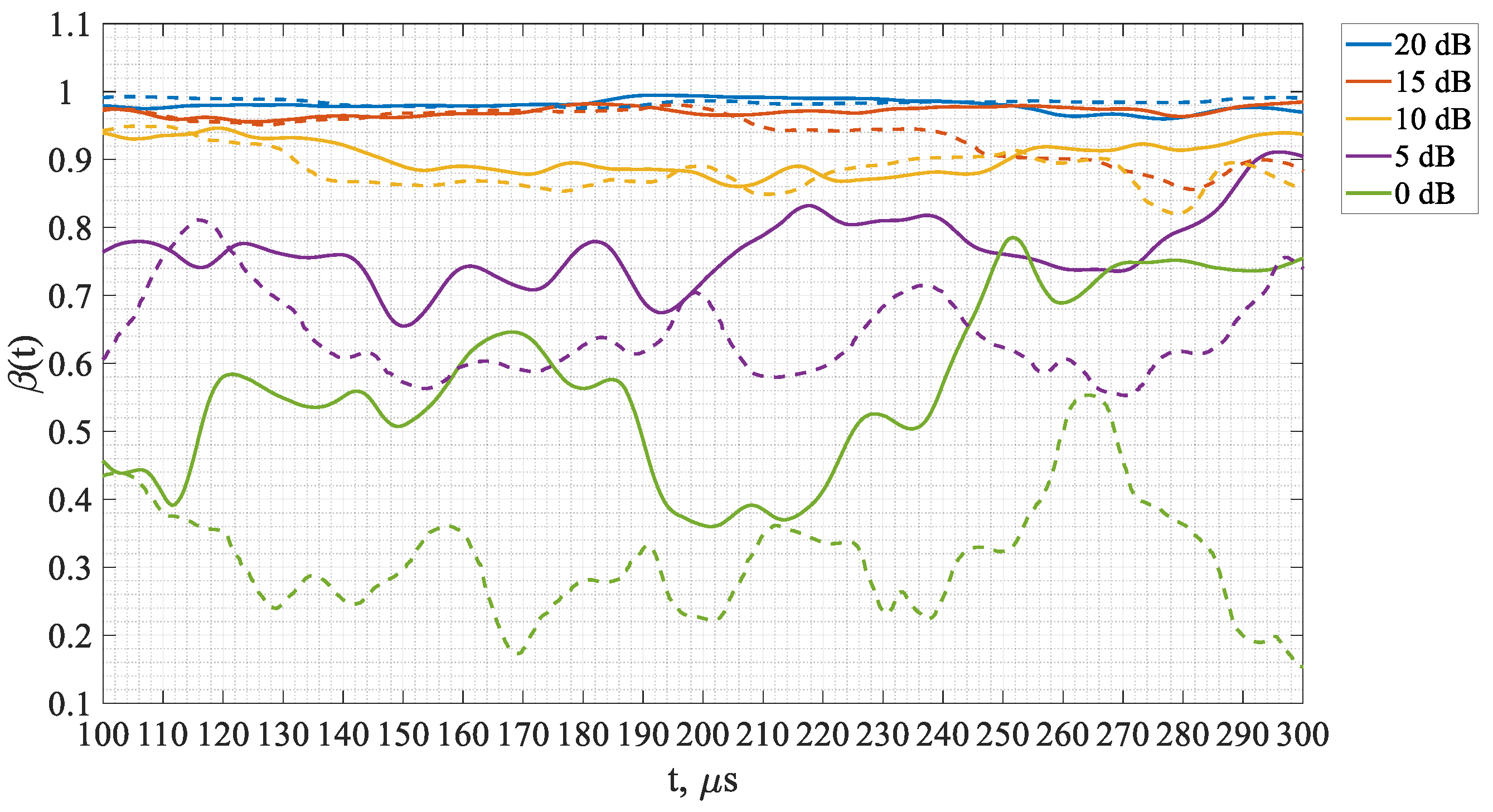
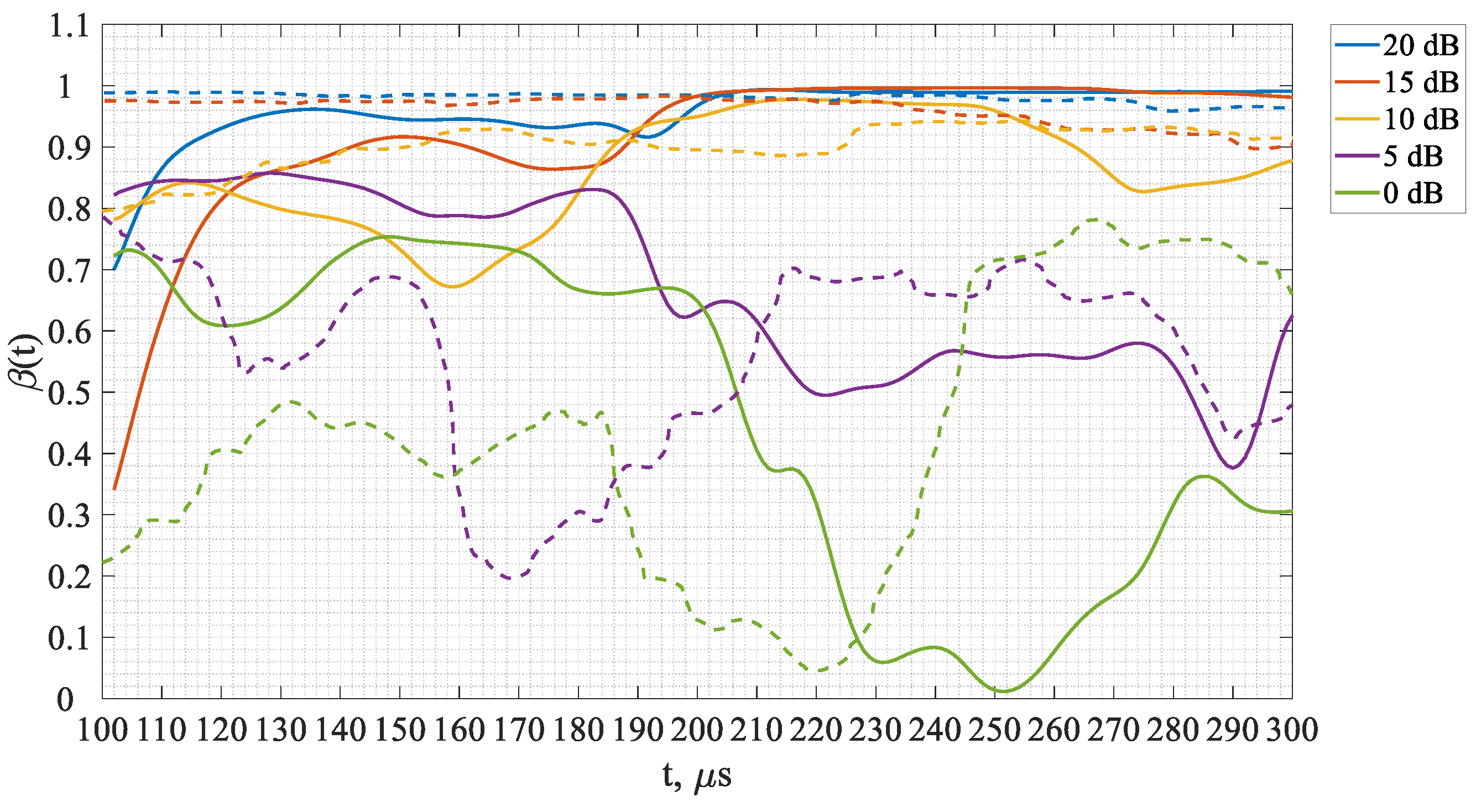
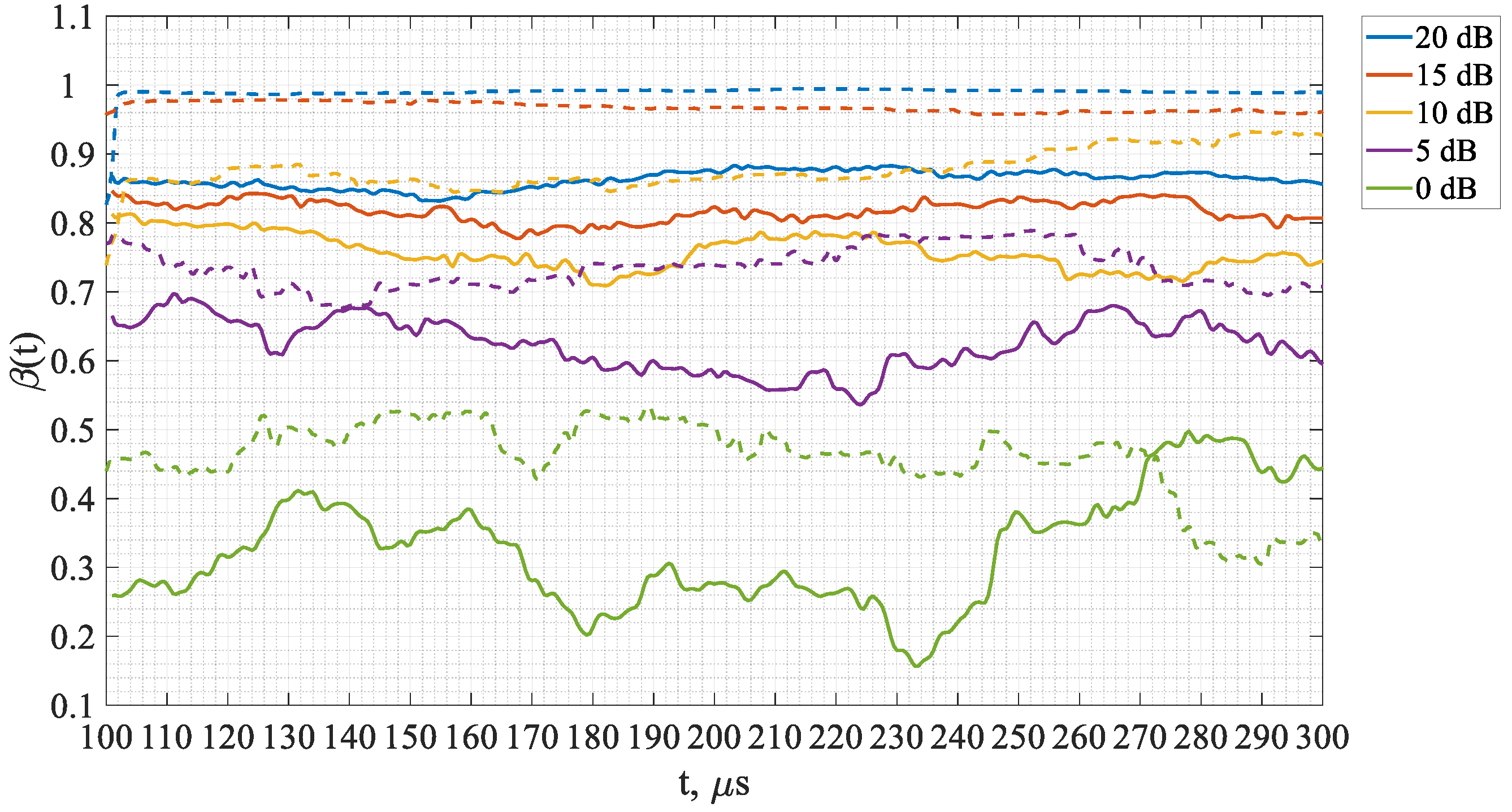
4.2. Hardware-Based Study

This section presents the hardware implementation (see Figure 5) of the experimental model shown in Figure 3. For the hardware experiment, the chaos oscillators are implemented in specially-designed PCBs. A pair of chaos oscillators is powered by two separate independent power supplies. The chaotic signal X 2 of the master oscillator is applied to the slave oscillator’s signal Y 2 through the synchronization circuit, which adds the n 2 noise signal to the applied X 2 signal. The design of the synchronization circuit is identical to the one used in the simulation setup in Figure 4. The Analog Discovery 2 (later referred to as AD2) devices were used in this experiment, labeled as AD2-X and AD2-Y [17].
AD2-X is employed to generate the n 1 noise signal that is added to the X 1 (W1), to apply power to the synchronization circuit (V+ and V−), and to record the X 1 and Y 1 voltage signals (Ch1 and Ch2). The AD2-Y purpose is to generate the n 2 noise signal that is added to the Y 2 signal in the synchronization circuit (W1) and to record the n 1 noise signal generated by the AD2-X (Ch1). To ensure the synchronous performance of the two AD2 devices, a dedicated application was created and run on the host computer, providing the execution of the mentioned tasks by AD2-X and AD-Y [17]. MATLAB software was used to sum the recorded n 1 and X 1 signals, resulting in the X 1 + n 1 signal, as well as to calculate the 100 μs window correlation coefficient between the X 1 + n 1 and the Y 1 signals. The noise pair n 1 , n 2 signal levels were measured from 20 dB to 0 dB SNR with a step of 5 dB. It is also important to notice that the X 1 , X 2 , Y 1 , Y 2 , for each chaos oscillator were the same as in the case of the simulation study.

4.3. Result Analysis

The current section summarizes and analyzes the results acquired in both simulation-based (Figure 4) and hardware-based (Figure 5) studies applied to RC1, RC2, and Vilnius chaos oscillators. The results for corresponding oscillators are presented in Figure 6, Figure 7 and Figure 8.
In Figure 6, Figure 7 and Figure 8, the 100 μs window correlation coefficient β over time since the beginning of synchronization is shown for different signal-to-noise ratios of the noise signal pair n 1 and n 2 . The first value of β is at 100 μs, as β has a 100 μs long window. As seen in all of the mentioned figures, in general, the achievable values of β tended to increase with the increasing of SNR, approaching perfect synchronization indicated by β = 1. This showed that lower noise levels allow better synchronization between the two chaos oscillators. If we compare the results of the three chaos oscillators only by the maximum achieved value of β at specific SNR levels, then the RC2 chaos oscillator was superior from this point—proven by peak values of β at SNR levels 0 dB and 5 dB. However, in Figure 6, Figure 7 and Figure 8, β curves fluctuate in simulation and hardware-based studies. These fluctuations are caused by the sufficiently high level of noise and the stability of oscillators themselves. The amplitude of fluctuations shows that some oscillators are more susceptible to noise. Vilnius chaos oscillator is superior from this point, as Figure 8 shows the least fluctuations. It is important to consider both: the maximum achievable value of β at a certain SNR level, as well as the fluctuations of the β curve at this SNR level.
By comparing the simulation results with those acquired in the hardware-based study for each chaos oscillator, the correlation among the results was obvious. Some minor differences in β curves for the same SNR levels in simulation and hardware were caused by the tolerances of the elements used in the hardware experiments and the incomplete models of the elements used in the simulation.
Observing the simulation and hardware-based results individually for each chaos oscillator, in the case of the RC1 chaos oscillator, the hardware results for SNR of 0 and 5 dB in Figure 6 are better than the simulation results for the corresponding SNR levels. The explanation is that for the low SNR levels, the fluctuation of the β curves is greater, which means the initial state of the system before the synchronization plays a crucial part in synchronization. In the case of the RC2 chaos oscillator in Figure 7, the fluctuation of the β curves for the SNR levels of 0 dB and 5 dB is even more severe. Even for the SNR levels 10–20 dB, the fluctuation is noticeable in simulation results and more explicitly in the hardware results. In the case of the Vilnius chaos oscillator in Figure 8, the fluctuations of the β curves are the least in comparison to all the chaos oscillators under research, which also means better synchronization noise immunity than for the other two chaos oscillators.
The conclusions from the results acquired in this study state that the level of synchronization of the chaos oscillators is decent even for the low signal to noise ratio and that the use of 100 μs as a time window for the correlation coefficient is sufficient for the determination of the correlation between two chaotic signals. None of the selected chaos oscillators simultaneously achieved maximal values of β along with low fluctuations of the β curves (e.g., Figure 6, Figure 7 and Figure 8 at SNR 0 to 10 dB). However, this step serves well as a first approach of estimating the performance of chaos oscillators with noise present during synchronization. This step can be applied to other chaos oscillators as an initial test of synchronization’s properties. Understanding the influence of chaotic synchronization’s noise immunity on a communication system’s level requires a more extensive study, provided in the next section.

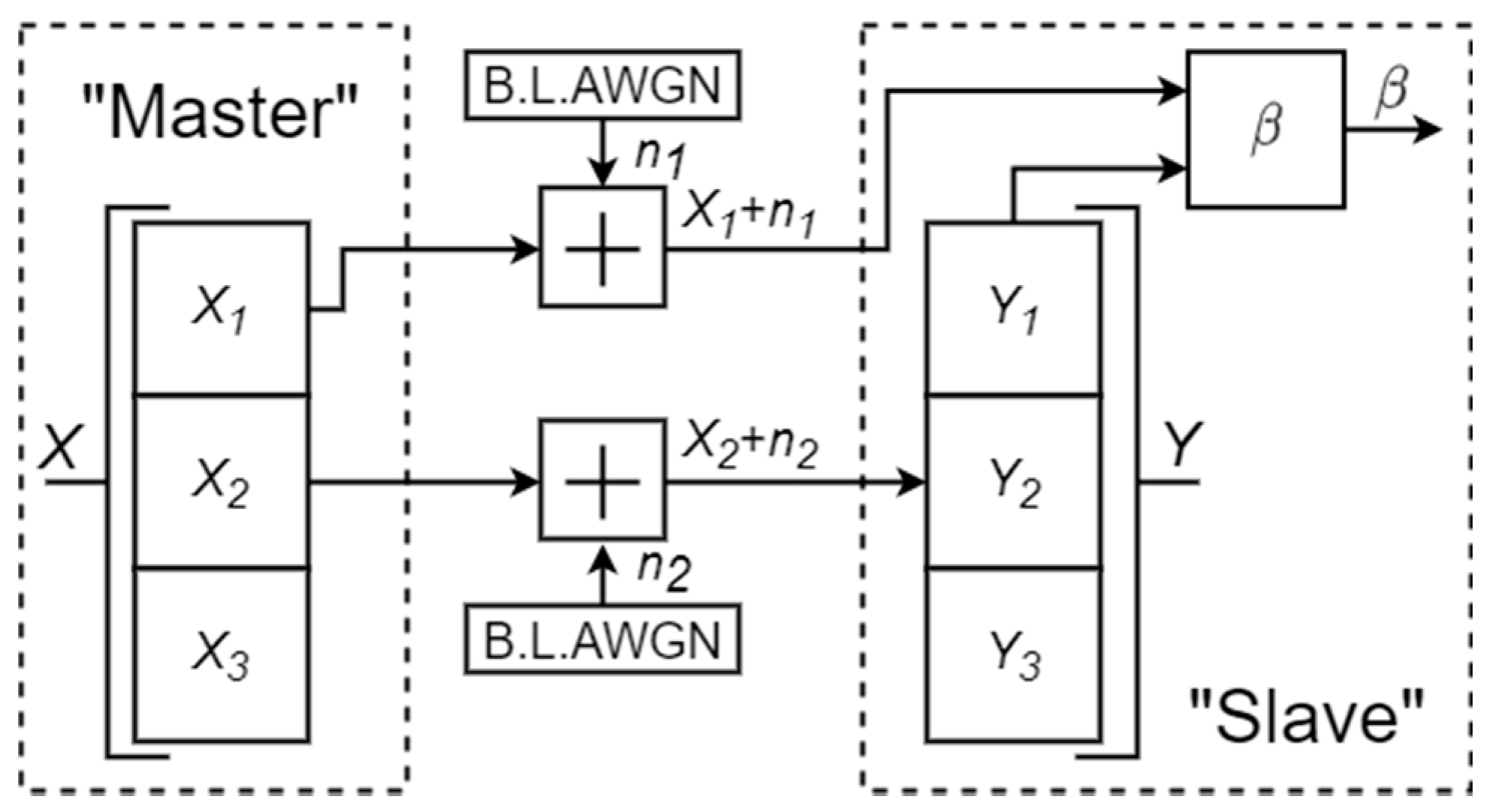
5. Performance of the Communication System

This section describes the second step in investigating the performance of the proposed communication system with the employment of the selected chaos oscillators. The second step of the research involves the investigation of the performance of the proposed communication system’s baseband model in the AWGN propagation channel. The model of the experiment is further described in detail.

5.1. Simulation-Based Study

The experimental model, presented in Figure 9, utilizes the baseband model of the communication system shown in Figure 1, excluding the quadrature modulator and demodulator. The noise being permanently present for X 1 PM and X 2 , assuming the worst-case scenario. X 1 PM represents state variable X 1 manipulated by m ( t ) message signal. When the “1” bit is transmitted, X 1 PM = X 1 , and when the “0” bit is transmitted, X 1 PM = X 1 .
For this experiment, the length of the message signal m ( t ) was 10 5 bits. The length of the correlation coefficient’s β window was 100 μs. The correlation coefficient’s β values are between −1 and 1; β = 1 when X 1 is received, and β = −1 when X 1 is received. The correlation coefficient is used to decode the message signal, the decoded received message signal m ( t ) ¯ = “1” if β > 0 , and m ( t ) ¯ = “0” if β < 0 . The performance of the system was estimated by calculating the bit error ratio (BER) for the transmitted message signal m ( t ) and the decoded received message signal m ( t ) ¯ for several energy per bit to noise power spectral density ratio (Eb/N0) levels. The frequency bandwidth of the noise signals n 1 and n 2 correspond to those of the signals X 1 PM and X 2 (see Figure 3). The state variables X 1 , X 2 , Y 1 , and Y 2 were the same for each chaos oscillator like in the previous experimental study. The propagation of both signals was simulated in the LTspice circuit simulator, whereas MATLAB was utilized for the calculations and analysis of the results.

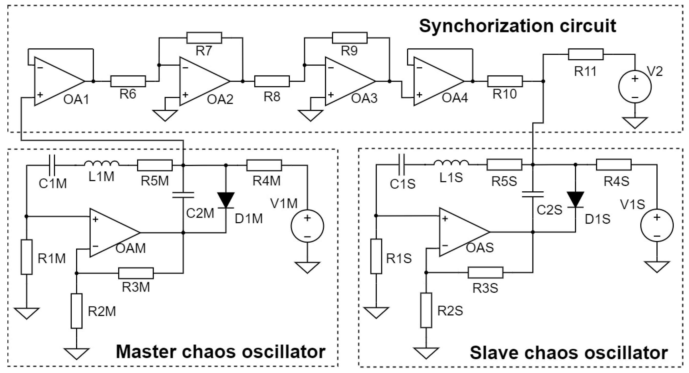
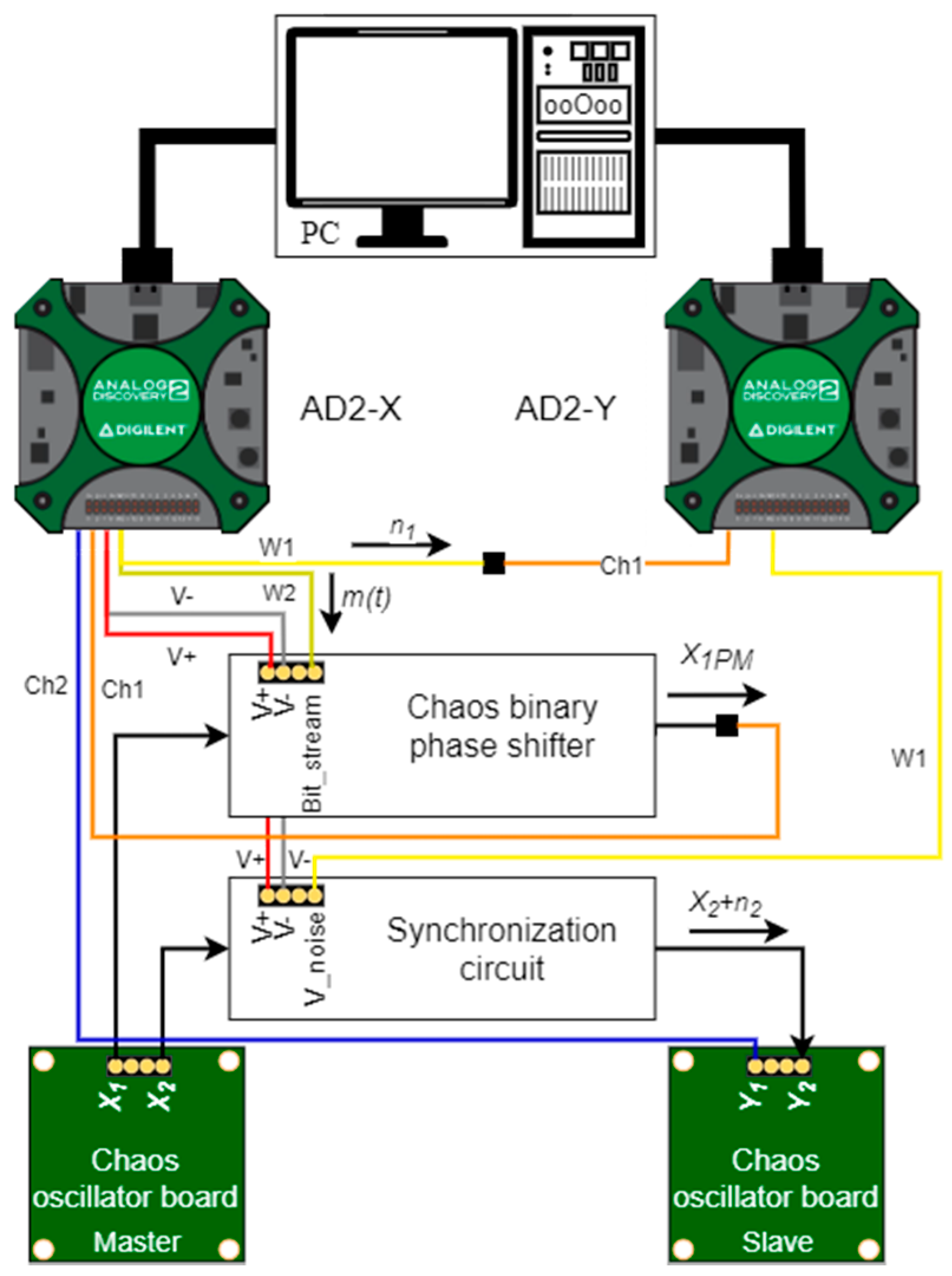
5.2. Hardware-Based Study

This section presents the hardware implementation (see Figure 10.) of the experimental model shown in Figure 9. The model is similar to the one shown in Figure 5 with some additions. A hardware binary phase shifter was introduced to manipulate the phase of the X 1 signal. AD2-X had an additional task of generating and applying information signals m ( t ) to the chaos binary phase shifter (W2). AD2-X records the X 2 phase manipulated and Y 1 voltage signals (Ch1 and Ch2). AD2-Y records the n 1 noise signal that is generated by the AD2-X (Ch1), similarly as in the previous hardware experiment.
This experiment was based on the hardware-in-the-loop approach since MATLAB was employed to sum the recorded n 1 and X 1 PM signals, giving the X 1 PM + n 1 signal. Moreover, MATLAB was employed to decode the message signal m ( t ) ¯ by applying a 100 μs window correlation coefficient between the X 1 PM + n 1 and Y 1 signals. BER is acquired by comparing decoded m ( t ) ¯ and original m ( t ) message signals. BERs were measured for all three chaos oscillators up to 11 dB Eb/N0, due to the hardware limitations.
The binary phase shifter’s circuit used for the hardware experiments is shown in Figure 11. The phase manipulation was based on the use of the ADG1219 analog switch circuit. Elements in Figure 11 have the following nominals: R 1 = R 2 = R 3 = 10 kΩ; C 1 = 10 nF; O A 1 O A 3 are TL082 operational amplifiers. The operational amplifiers were utilized to acquire an inverted and direct X 1 . C 1 and R 1 form a high-pass filter that removes the DC component from X 1 signal. O A 1 is employed as a buffer to isolate the high-pass filter from the chaos oscillator circuit. ADG1219 serves as a switch between inverted and direct X 1 according to the m ( t ) ; thus, the X 1 PM signal forms on the output of the ADG1219.

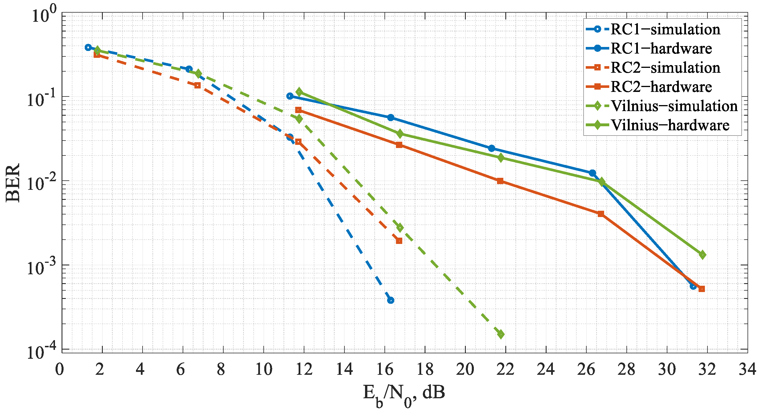
5.3. Result Analysis

This section is dedicated to the analysis of the results acquired in simulation and hardware experimental studies. The results are presented in Figure 12 for the proposed communication system’s baseband experimental study of the model in the AWGN channel.
In Figure 12, the BERs over energy per bit to noise power spectral density ratio Eb/N0 are shown for all three selected chaos oscillators employed as chaotic X and Y systems. Figure 12 reflects superior simulation results of the system using the RC2 chaos oscillators compared to the other two chaos oscillators. For Eb/N0 12–17 dB, the system based on the RC1 chaos oscillators demonstrated better results than in the case of the other two chaos oscillators. At the point of Eb/N0 around 22 dB, the RC1 and RC2 based systems provided error-free communication. Overall, the RC2 chaos oscillator demonstrated the best performance in the simulation.
The results in hardware naturally demonstrated a greater number of error bits than the circuit simulation results, which is expected, as hardware implementation of chaos oscillators and other functional blocks introduced many parasitic parameters and imprecisions, compared to the simulation. It is important to notice that hardware results showed greater BER where simulation demonstrated error-free communication. However, the hardware results follow that the RC2 chaos oscillator demonstrated the worst performance among the three chaos oscillators, whereas the RC1 chaos oscillator had superior performance compared to other ones. Results in Figure 6, Figure 7 and Figure 8 show that the lower SNR allows better synchronization, which in Figure 12 corresponds to a lower number of error bits and better BER (SNR and Eb/N0 are closely related). As noise level increases, the quality of synchronization decreases—depicted by lower β values and increased fluctuations in Figure 6, Figure 7 and Figure 8. This corresponds to a greater number of error bits and worse BER in Figure 12. The results of the two studies correlate and give a better understanding of how the noise impacts the proposed CQPSK system.

6. Conclusions

Research done in the current paper was aimed at investigating the impact of the chaotic synchronization on the performance of the quadrature transceiver-based communication system that utilizes chaotic signals for data transmission. For this study, we chose RC1, RC2, and Vilnius chaos oscillators and studied their synchronization noise immunity as a first step of the research. The results have shown that the synchronization’s noise immunity properties of the chaos oscillators are sufficient in potential employment for data transmission in low-complexity secure communication systems. We performed a comparison between the communication system hardware implementation with simulation to estimate the influence of the chaos oscillator’s properties on the performance of the quadrature transceiver-based communication system in the AWGN channel. The results in this step revealed notable differences between simulation and hardware BERs. The employment of the 3 different chaos oscillators yielded comparable results, with the RC2 chaos oscillator showing superior performance in simulation, whereas the RC1 chaos oscillator showed superior performance in hardware.
The research presented in this paper opens possibilities to use such systems in IoT and WSNs, as the non-periodic, noise-like behavior of chaotic systems adds a physical layer of security in communication. The further research steps will be aimed at implementing a narrowband communication system for WSN.

Author Contributions

Conceptualization, A.A. and A.L.; Funding acquisition, A.L.; Investigation, R.B., D.C., and M.Z.; Software, R.B., J.G., and A.A.; Supervision, A.L.; Validation, J.G.; Visualization, D.C. and D.P.; Writing—original draft, R.B.; Writing—review & editing, A.A., D.P., and A.L. All authors have read and agreed to the published version of the manuscript.

Funding

This work has been supported by the European Regional Development Fund within the Activity 1.1.1.2 “Post-doctoral Research Aid” of the Specific Aid Objective 1.1.1 “To increase the research and innovative capacity of scientific institutions of Latvia and the ability to attract external financing, investing in human resources and infrastructure” of the Operational Program “Growth and Employment” (No.1.2/VIAA/2/18/345).

Conflicts of Interest

The authors declare no conflict of interest.

References

  1. Dorogovs, P.; Romanovs, A. E-Service Security Challenges: Availability, Integrity, Confidentiality. Balt. J. Mod. Comput. 2016, 4, 68. [Google Scholar]
  2. Romanovs, A.; Soshko, O.; Merkuryev, Y. Information technology focused training in logistics. In Proceedings of the 2010 9th International Conference on Information Technology Based Higher Education and Training, Cappadocia, Turkey, 29 April–1 May 2010. [Google Scholar]
  3. Litvinenko, A.; Aboltins, A.; Pikulins, D.; Ahrens, A.; Capligins, F.; Eidaks, J. Advanced Chaos Shift Keying Based on a Modified Chua’s Circuit. In Proceedings of the 2019 IEEE Microwave Theory and Techniques in Wireless Communications, Riga, Latvia, 1–2 October 2019. [Google Scholar]
  4. Anstrangs, D.D.; Cirjulina, D.; Babajans, R.; Tjukovs, S.; Litvinenko, A. Encoded Chaos Shift Keying Communication System. In Proceedings of the 2020 IEEE Microwave Theory and Techniques in Wireless Communications (MTTW), Riga, Latvia, 1–2 October 2020. [Google Scholar]
  5. Zhu, S.; Xu, Y.; Yin, K. Design of a quadrature differential chaotic phase shift keying communication system. In Proceedings of the International Conference on Networks Security, Wireless Communications and Trusted Computing, Wuhan, China, 25–26 April 2009. [Google Scholar]
  6. Giurcăneanu, C.D.; Abeywickrama, R.V.; Berber, S. Performance analysis for a chaos-based code-division multiple access system in wide-band channel. J. Eng. 2015. [Google Scholar] [CrossRef]
  7. Mesloub, A.; Boukhelifa, A.; Merad, O.; Saddoudi, S.; Younsi, A.; Djeddou, M. Chip Averaging Chaotic ON-OFF Keying: A New Non-Coherent Modulation for Ultra Wide Band Direct Chaotic Communication. IEEE Commun. Lett. 2017. [Google Scholar] [CrossRef]
  8. Cai, X.; Xu, W.; Miao, M.; Wang, L. Design and Performance Analysis of a New M -Ary Differential Chaos Shift Keying with Index Modulation. IEEE Trans. Wirel. Commun. 2020. [Google Scholar] [CrossRef]
  9. Ma, H.; Cai, G.; Fang, Y.; Wen, J.; Chen, P.; Akhtar, S. A New Enhanced Energy-Detector-Based FM-DCSK UWB System for Tactile Internet. IEEE Trans. Ind. Inform. 2019. [Google Scholar] [CrossRef]
  10. Stavroulakis, P. Chaos Applications in Telecommunications; CRC Press: Boca Raton, FL, USA, 2005; ISBN 9780203025314. [Google Scholar]
  11. Liya, D.; Yonghong, H. Performance analysis for multiple access coherent chaos-shift-keying system. In Proceedings of the 5th International Conference on Wireless Communications, Networking and Mobile Computing, Beijing, China, 24–26 September 2009. [Google Scholar]
  12. Pandey, A.; Dahate, S. Secure communication using a modified chaotic masking scheme employing Sprott94 case a chaotic attractor. In Proceedings of the 2014 2nd International Conference on “Emerging Technology Trends in Electronics, Communication and Networking”, Surat, India, 26–27 December 2015. [Google Scholar]
  13. Tamaševičius, A.; Mykolaitis, G.; Pyragas, V.; Pyragas, K. A simple chaotic oscillator for educational purposes. Eur. J. Phys. 2005. [Google Scholar] [CrossRef] [Green Version]
  14. Namajunas, A.; Tamaševičius, A. Simple RC chaotic oscillator. Electron. Lett. 1996. [Google Scholar] [CrossRef]
  15. Keuninckx, L.; Van Der Sande, G.; Danckaert, J. Simple Two-Transistor Single-Supply Resistor—Capacitor Chaotic Oscillator. IEEE Trans. Circuits Syst. II Express Briefs 2015. [Google Scholar] [CrossRef]
  16. Babajans, R.; Anstrangs, D.D.; Cirjulina, D.; Litvinenko, A.; Pudzs, M. Chaotic Synchronization for Data Transmission Systems. In Proceedings of the 2019 IEEE 7th IEEE Workshop on Advances in Information, Electronic and Electrical Engineering (AIEEE), Liepaja, Latvia, 15–16 November 2019. [Google Scholar]
  17. Babajans, R.; Anstrangs, D.D.; Cirjulina, D.; Aboltins, A.; Litvinenko, A. Noise Immunity of Substitution Method—Based Chaos Synchronization in Vilnius Oscillator. In Proceedings of the 2020 IEEE Microwave Theory and Techniques in Wireless Communications (MTTW), Riga, Latvia, 1–2 October 2020. [Google Scholar]
  18. Kolumbán, G.; Kennedy, M.P.; Chua, L.O. The role of synchronization in digital communications using chaos—PART II: Chaotic modulation and chaotic synchronization. IEEE Trans. Circuits Syst. I Fundam. Theory Appl. 1998. [Google Scholar] [CrossRef] [Green Version]
  19. Chua, L.O.; Itoh, M.; Kocarev, L.; Eckert, K. Chaos synchronization in chua’s circuit. J. Circuits Syst. Comput. 1993. [Google Scholar] [CrossRef]
Figure 1. Block diagram of the quadrature chaos phase-shift-based communication system [16].
Electronics 10 00640 g001
Figure 2. Circuit diagrams of the RC1 chaos oscillator (a), RC2 chaos oscillator (b), Vilnius chaos oscillator (c) [14,15,16,17].
Electronics 10 00640 g002
Figure 3. Block diagram of the experimental study of the noise immunity of chaos oscillator’s synchronization [16].
Electronics 10 00640 g003
Figure 4. Simulation setup for the experimental study of the noise immunity chaos oscillator’s synchronization with a pair of Vilnius chaos oscillators as an example [17].
Electronics 10 00640 g004
Figure 5. Hardware setup for the experimental study of the noise immunity of the chaos oscillator’s synchronization [17].
Electronics 10 00640 g005
Figure 6. Hardware (solid lines) and simulation (dashed lines)-based results for the experimental study of the noise immunity of the RC1 chaos oscillator’s synchronization.
Electronics 10 00640 g006
Figure 7. Hardware (solid lines) and simulation (dashed lines)-based results for the experimental study of the noise immunity of the RC2 chaos oscillator’s synchronization.
Electronics 10 00640 g007
Figure 8. Hardware (solid lines) and simulation (dashed lines)-based results for the experimental study of the noise immunity of the Vilnius chaos oscillator’s synchronization [17].
Electronics 10 00640 g008
Figure 9. Block diagram of the proposed communication system’s experimental study in the additive white Gaussian noise (AWGN) propagation channel.
Electronics 10 00640 g009
Figure 10. Hardware model of the proposed communication system’s experimental study in the AWGN propagation channel.
Electronics 10 00640 g010
Figure 11. Chaos binary phase shifter.
Electronics 10 00640 g011
Figure 12. Estimation of communication system’s performance in the AWGN channel using 3 different chaos oscillators.
Electronics 10 00640 g012
Publisher’s Note: MDPI stays neutral with regard to jurisdictional claims in published maps and institutional affiliations.

