
Two Decades of Condition Monitoring Methods for Power Devices


1
Department of Electrical Electronic and Computer Engineering (DIEEI), University of Catania, Viale Andrea Doria, 6, 95125 Catania, Italy
2
Department of Energy Technology, Aalborg University, 9220 Aalborg, Denmark
*
Author to whom correspondence should be addressed.
Electronics 2021, 10(6), 683; https://doi.org/10.3390/electronics10060683
Submission received: 1 January 2021
/
Revised: 15 February 2021
/
Accepted: 24 February 2021
/
Published: 15 March 2021
(This article belongs to the Special Issue Challenges and New Trends in Power Electronic Devices Reliability)
Abstract
:Condition monitoring (CM) of power semiconductor devices enhances converter reliability and customer service. Many studies have investigated the semiconductor devices failure modes, the sensor technologies, and the signal processing techniques to optimize the CM. Furthermore, the improvement of power devices’ CM thanks to the use of the Internet of Things and artificial intelligence technologies is rising in smart grids, transportation electrification, and so on. These technologies will be widespread in the future, where more and more smart techniques and smart sensors will enable a better estimation of the state of the health (SOH) of the devices. Considering the increasing use of power converters, CM is essential as the analysis of the data obtained from multiple sensors enables the prediction of the SOH, which, in turn, enables to properly schedule the maintenance, i.e., accounting for the trade-off between the maintenance cost and the cost and issues due to the device failure. From this perspective, this review paper summarizes past developments and recent advances of the various methods with the aim of describing the current state-of-the-art in CM research.
1. Introduction
Nowadays, power electronics is widespread in a huge number of daily applications that improve services for the collective [1]. Furthermore, power electronics has a key role in renewable energy systems [2,3], lighting [4,5], electric mobility [6,7], and other systems that enable sustainable development [8].
A crucial aspect is the reliability and lifetime prediction of the whole power conversion system. The warrant of the highest robustness level while minimizing the product and maintenance cost is extremely mandatory. For example, the devices used in avionic and automotive applications must have a fault rate close to zero that imposes stringent requirements during the system design. In the same way, wind farms must guarantee normal operations without interruption, but this is extremely difficult because of the expensive access to farms for easier maintenance. In this context, many approaches to forecasting the lifetime of power electronic systems and the single power device have been intensively studied.
To guarantee a high level of reliability, it is important to comply with several standards [9,10,11], and different strategies are usually performed such as the use of the fault-tolerant topologies with redundant components [12,13], and the advanced reliable design of power electronic devices using innovative materials [14,15].
Unfortunately, the enhanced system’s robustness does not prevent failure and, indeed, it is never completely foreseeable. Therefore, a maintenance operation before a failure is necessary. Considering the costs of maintenance operations, lifetime prediction combined with condition monitoring approaches [16,17] are very useful tools to choose when a maintenance operation has to be carried out.
Some studies have shown that capacitors are fragile with a failure of 30%, whereas the failure of the PCB and connectors is around 36% [18,19,20]. The remaining part is related to the semiconductor and soldering failures in device modules that consist of the most important area of concern for converter system failures. In this context, countless condition monitoring (CM) methods for the evaluation of the semiconductor state of health have been widely explored in the literature.
The target of this work is to provide an overview of various CM methods that have been used to evaluate the state of the health of power devices. More specifically, the first part of the proposed review was focused on the impact of the Internet of Things (IoT) and artificial intelligence (AI) technologies used for CM of power devices, with a chronological overview of the main CM methods over the last two decades. Then, it a first CM method based on acoustic emission was presented and used to detect any physical damage in a power module packaging. It is worth underlining that it enables one to estimate the state of aging of a power module.
Then, CM methods based on the optical properties of the semiconductor power devices were presented, including temperature estimation. These methods are usually based on an optical beam that is reflected or scattered back from the semiconductor lattice. There is an inherent dependence between the temperature and the energy related to the photoemission. More specifically, such energy is a function of the junction temperature (JT); hence, in turn, the energy variation can be used to estimate the temperature of the chip. After that, a depth-analysis of the several approaches to extract the junction temperature in the semiconductor devices based on the physical or electrical properties was performed. The early works using a physical CM method for the JT measurement were done by directly contacting the chip surface with a thermo-sensitive material such as a point contact system (such as thermocouples and liquid crystal). On the other hand, electrical methods for the junction temperature measurement are often the preferred choice for CM of power devices because the temperature estimation can be carried out through the measurement of electrical quantities. Among various electrical CM methods, thermal test chips (TTCs) are directly fabricated on the die surface of the device, and the voltage drop can be used to estimate the temperature variations. On the other hand, the temperature sensitive electrical parameters (TSEPs) are based on the measurement of the voltage drop during the converter operations. Generally, the measurement of the voltage drop can be carried out using some voltage probes connected to the device terminals.
Although the measurement of the power devices’ junction temperature was widely treated in many ways, it is still an active relevant topic owing to the current trade-off between the advantages and limitations of the methods proposed so far. Therefore, all these methods have been compared in terms of their main aspects such as sensitivity, linearity, cost, and online monitoring operations.
2. Conditioning Monitoring Methods and Their Future Application
In the literature, the research topic based on CM methods has been gaining interest as the various maintenance strategies allow to increase the lifetime of the overall power conversion system. In many applications, it is becoming crucial to monitor the state of the health (SOH) of power devices to prevent a failure, that is, the possibility for the operators to obtain a lifetime estimation, thus properly scheduling any maintenance operations.
Figure 1 depicts a timeline of the various CM methods for power devices that have been widely studied in the literature and used by the industry in the last two decades. The first use of CM methods for power devices dates back to the 2000s, where the measure of on-state voltage of the devices was used as a well-known parameter to monitor the device condition. Later, the measure of the threshold voltage or the gate turn-off voltage of a device was used to estimate the temperature dependence of the power devices by measuring a low voltage; then, the acquisition system was developed to be more simple and less bulky. In the last 5 years, the estimation of the SOH has been carried out using contactless approach such as the acoustic method or the photodiode approach, where the acoustic emission or the light emission, respectively, of a particular device have been taken into account.
The thermal stresses such as the increasing of the mean temperature and abrupt temperature fluctuations are the main failure mechanisms. Consequentially, the temperature is an index of the power device SOH. Other CM methods focus on other quantities. Table 1 summarizes the physical or electrical quantities measured for each CM method and, in the following subsections, a brief overview is presented. It is worth noting that, among the various CM methods in the literature, the acoustic one is used to detect the state of the aging of the power device without any estimation of the working temperature, while all the other strategies are focused on the estimation of the junction temperature (JT). More specifically, some CM methods perform such estimation by directly measuring the temperature, such as the infrared (IR) camera, a negative temperature coefficient (NTC) resistor, fiber optic cable, and photodiodes sensors. Other methods provide an indirect estimation by mapping electrical quantities in a temperature value, such as the thermo-sensitive electrical parameters (TSEPs).
According to recent research, the emerging trend of IoT and AI technologies are gaining more and more interest and they are expanding rapidly in the field of CM methods [21].
AI aims to assist electronic systems with intelligence that is capable of human-like learning and reasoning. This technology possesses countless advantages and has been widely applied in numerous industrial and research areas such as maximum power point tracking (MPPT) control for Photovoltaic (PV) plants, anomaly operation detection for inverter, and prediction of the SOH of a power converter.
The use of enabling AI technologies allows the power converter systems to be embedded with capabilities of self-awareness and self-adaptability, thus system autonomy can be enhanced. Similarly, the development of data science, including sensor technology, IoT, and big data analytics, provides a wide variety of data for power electronic systems throughout different stages of its life-cycle. Furthermore, AI technology can exploit data to estimate the system health status with high sensitivity in condition monitoring for aging detection of power devices. Only in a few works [22,23,24,25] has the condition monitoring and fault detection in power electronics AI-based fault detection been presented.
Figure 2 shows a proof-of-concept of the integration between IA and IoT technologies for CM of power devices. More specifically, Figure 2a depicts an example of a user (red box), which consists of a specific power converter and its power devices that have to be monitored, and an example of a provider of CM services (PS) (yellow block). More specifically, the devices of a single-user power application are connected with several sensors that enable the monitoring of the SOH of each device (such as the measurement of the TJ or the state of aging of a device). Then, the controller system interface (CSI) manages the sensors and collects all the measured data. The CSI block plays an important role for the CM of the power system because it is able to provide control signals and it may exchange data with different users in the IoT framework (see Figure 2b).
The PS (sometimes also the CSI) uses AI technologies that act as “intelligent agents”, exploiting sensors able at perceiving the environment of the power converter. Indeed, during some power converter operations, the JT can be dangerously increased over a threshold maximum value, hence the AI is able to suddenly shut down the power system. Moreover, the AI-integrated system may enable a power derating in order to avoid any failure of the converter and, hence, the power devices. On the other hand, AI should perform more complex tasks, such as detecting any change in the device behavior that could lead to future malfunctioning; interacting with the CSI “to propose” solutions, i.e., fault preventing strategies, to current anomalies or potential future ones; and so on. Regardless of whether AI is located in the PS, in the CSI, or both, a local backup control system is necessary. The local controller should be simple (without complex hardware and control strategies) and highly reliable. The local controller should have less stringent limits than the AI, thus the local controller intervenes only when the system is close to a dangerous situation. For example, the local converter shuts down the converter when the JT passes over a preset limit and this situation occurs owing to the lack of a smarter command (load reduction, switching frequency variation, and so on) from the AI of the PS because of different causes (e.g., temporary lack of connection, unexpected AI actions or reasoning).
It is worth noting that the PSs are able to contribute to the decision making in both offline and real-time analysis using data acquired in the past and saved into a dedicated database (green silos). From this perspective, all the collected data can be used to enhance the predictive model of the SOH of the power devices.
Moreover, the PS may interact with enterprises, authorities, public companies, and so on. For example, real-time use of CM occurs when a PS notices a critical functioning of the converters of a large PV system. The PS informs the PV owner as well as interacts with the PV management system to enable them to promptly and properly operate. On the other hand, the PS also informs the electric network operator (ENO) of the smart grid where the PV is installed about a potential disconnection of the PV system. This information enables the ENO to adopt countermeasures that mitigate the impact of such a disconnection. In turn, the ENO informs sensitive customers, e.g., hospitals, of a potential lack of service or asks them to turn on a backup system in order to reduce the absorbed power.
Furthermore, the measurements of the JT and other parameters of the power devices can be used by some public institutions such as universities or research centers (blue pale and red dashed lines) for an off-line analysis of the data to carry out some models of the SOH of the power devices. Moreover, the PS may be connected to a security organization (grey dashed lines) that may collect data and it should be able to interrupt an electrical service in the case of failure.
It is worth underlining that the PSs could provide data to the power device manufacturers with the aim to share information related to the state of aging of the power devices. The manufacturers can use the data to improve their power devices as well as to obtain more accurate power device models. Indeed, manufacturers can act as PSs.
3. Acoustic Methods
Acoustic emission has been widely investigated in the literature as a CM quantity useful in different application fields such as pumps, industrial electrical machines, and so on. Moreover, in the field of power electronics, acoustic monitoring has been extensively used to detect any defects or damage in transformers and capacitors [25,26,27]. Only in the last decade, a few works have been focused on the acoustic phenomenon such as a measurement method for monitoring the SOH of the power semiconductor devices [28,29,30,31,32,33].
Acoustic emission has been used to detect any physical damage in a power module packaging using an acoustic microscope. Furthermore, from the experimental evidence, it has been proven that acoustic emissions are related to the switching operations of power devices. In the case of fast switching operation (tens of nanoseconds), a certain amount of current is switched, which causes a large di/dt, which involves magnetic interaction within the module packaging. This means that the magnetic force could be the source of the acoustic emission, such as the mechanical breaking of the structure inside the component package. However, the physical phenomena causing the acoustic emission are not definitively understood.
Thereby, the device under test (DUT) is monitored contactless with an acoustic sensor that is usually placed in the proximity of the package. It intrinsically eliminates the issues related to contact directly with the voltage probes.
A correlation between the SOH of the power module and the analysis of its acoustic emission during the switching process has been analyzed [28,29,30]. It has been demonstrated that the acoustic peak in an aged device is smaller in comparison with a new one. However, in these works, only the acoustic emission of an Insulated Gate Bipolar Transistor (IGBT) connected into short-circuit has been investigated. Meanwhile, the authors of [32] present an early experimental setup used to prove that acoustic emission is related to the switching of power semiconductor components. Furthermore, the authors have proposed an analysis based on propagation delays to assess the source of the acoustic emission. The authors in [33] have investigated the acoustic emission as a CM method to measure the fatigue mechanisms in the power module. More specifically, they have investigated the physical degradation, observing the aging process of the whole power module by measuring the frequency spectrum of acoustic emission. The authors in [34] have measured the acoustic emission during converter operations to estimate the aging of a power semiconductor module due to power cycling. However, a spectrum analysis has been conducted to process the acquired data. The experimental results have shown a correlation between acoustic emission and the drain-source voltage, which is a common indicator of degradation of the bond wires of the power module.
As for disadvantages, the acoustic method needs an expensive and complex sensing circuit to correctly decode the acoustic emission. Furthermore, the system has to be shielded against Electromagnetic interference (EMI) and the superposition of noise contributions.
4. Optical Methods
Temperature variation, especially the sudden increase of the JT, plays a significant role in terms of power device reliability [34,35]. CM methods performing on-line JT monitoring raise great interest in terms of planning maintenance operations because the working conditions of a power converter are extremely unpredictable. From this perspective, the CM methods based on the optical properties of the semiconductor power devices were studied in depth because they are useful for temperature estimation. These methods are usually based on an optical beam that is reflected or scattered back from the semiconductor lattice. There is an inherent dependence between temperature and the energy related to the photoemission. More specifically, such energy is a function of the JT, hence, in turn, the energy variation can be used to estimate the temperature of the chip. It is worth remembering that these solutions based on optical quantities have some other drawbacks, such as the high cost and the impracticality in high-voltage converters.
There are various techniques for thermal mapping based on the use of an IR sensor [36,37,38,39,40], IR microscope [41], 2D radiometry [41,42], and the laser deflection technique [43,44,45], while fiber optic [46,47,48] and the IR camera [49,50,51,52,53,54] can both be used to obtain a thermal mapping or the JT value. In the following, the aforementioned optical techniques are briefly discussed.
4.1. Infra-Red/Visible Emission
An IR sensor is able to detect changes in the amount of infrared radiation of an object, which may vary depending on the temperature and surface characteristics of the objects in front of the sensor. The use of the IR sensors as a CM method for the measurement of the JT in a power device [36,37,38,39] is almost inexpensive as well as not very intrusive. However, these sensors have a low response time and, furthermore, the IR sensors average out the junction temperature value of the power device, and hence the accuracy is very low.
On the other hand, the emerging trend of the Wide-bandgap (WBG) power devices, such as the SiC power MOSFETs, are more and more diffusing devices as they concurrently enable high switching frequency, high voltage, and high-temperature operations. Therefore, the study of the electroluminescence proprieties of the SiC material for on-line CM has started to attract wide interest. For different reasons, the electroluminescence proprieties have already been studied back in 1907 [55], while, in the last three years, the inadvertent light emission phenomenon in the intrinsic body diode has drawn attention. While the body diode is in forward conduction mode, the chip glows a visible blue light [56]. The light brightness of the SiC body diode strongly depends on both the injected current magnitude and the JT. Hence, the measurement of light brightness can be used as a novel CM method for temperature detection, where only a few works have already focused on this topic [56,57,58]. The first proof of concept of the SiC light emission in a commercial power module has already proven the potentiality of this CM method [57]. An inexpensive passive sensing circuit, such as a silicon photodiode and a resistor, was adopted and the photodiode output voltage was correlated to the light emission intensity as a function of the temperature. It is worth noting that the system is small enough such that it can be easily embedded in the package. Another approach considers a light circuit sensing using two commercial photodiodes with an active signal conditioning circuit [58]. This approach has been adopted for JT estimation in a real application such as a pulse-width modulation (PWM) driven converter. The temperature-dependent changes in the spectrum of the light emission from the body diode of a SiC module have also been investigated [59]. The method has been proven through static characterization and dynamic double pulse measurement using two silicon photomultipliers, which can detect the peak intensity and, consequentially, the temperature dependence. Different from the previous CM methods, the last one, based on the light intensity of the SiC body diode, enables high-voltage operations and, even more importantly, the JT can be estimated during on-line operations.
4.2. Optical Fibers
The use of optical fiber as a CM method for the power modules has been discussed in very few works [46,47,48]. It is worth underlining that this CM method can be used without removing the dielectric gel on the power module surface, and the JT can be measured by placing the fiber optic cable in direct contact with the power chip. On the other hand, the measure is able to give only a local temperature; further, for almost all fiber optic methods, the measurement response time is generally high. Furthermore, it requires an external conditioning circuit unit that may be bulky for a specific application.
As an example, in [49], an optical fiber sensor has been used to measure the die temperature of an IGBT power module to estimate the thermal impedance (see Figure 3). The module top lid has been removed because the optical system has to be placed close to the die. Printing the die and bond-wires to increase the emissivity of the chip is usually preferable, but causes a cost increment and severely limits the on-line use of the method.
4.3. IR-Detection Apparatuses
IR-detection apparatuses are not really used as a CM method for power devices, but are extremely useful in laboratory testing (e.g., under power cycling) [49,50,51,52,53]. More specifically, the use of an IR camera allows to display the thermal map of the whole surface of the power module under test, as shown in Figure 4. As expected, the module temperature is not uniformly distributed; the temperature gradient between the center and the edge of the module can be greater than 40 °C. Usually, an IR camera is used to carry out a spatial thermal mapping on the device surface, but it is not able to provide an accurate measure of the device JT. It is worth remembering that some temperature measurement errors can be done using an IR camera because of the surface degradation of materials and the intrinsic low emissivity of aluminum. Even in this case, the IR temperature measurements are usually conducted by varnishing the surface of the DUT with a particular solution that increases the thermal emissivity on the surface.
4.4. Other Techniques
The IR microscope [40], 2D radiometry [41,42], and the laser deflection technique [43,44,45] have also been used as CM methods for power devices. All the aforementioned methods are able to provide a very precise JT estimation of a semiconductor device, but, on the other hand, the devices under test are to be driven with a specific testing sequence, not matching with the real operation in a power converter. They are also very expensive solutions and are not easily embedded in a real application.
Among the various sensors that use the 2D radiometry and laser deflection technique, it is worth remembering the InSb photovoltaic detector, which is a high-speed, low-noise infrared detector that delivers high sensitivity, and with an optical microsensor whose operating principle is based on detecting the absorption, deflection, and phase shift of an optical beam.
5. Physical Methods
The early works treating CM methods for the JT measurement have been done by directly contacting the chip surface with a thermo-sensitive material such as a point contact system. In this case, direct access to the semiconductor chip is necessary and, consequentially, the package must be removed.
Various equipment has been used for the physical contact measurement, including thermocouples, thermistors, scanning thermal probes, and multiple contact or blanket coatings such as liquid crystals and thermographic phosphors [59,60,61,62,63,64,65]. The aforementioned equipment relies on the transfer of thermal energy from the DUT to the thermal sensors. In this case, the spatial resolution related to the contact measurements strictly depends on the size and the thermal capacitance of thermo-sensible materials. The ability to provide a temperature map utilizing a matrix of sensors and a wide spatial resolution (can reach less than 100 nm) are the main advantages. In the following, the aforementioned physical techniques have been briefly discussed.
5.1. Thermocouples
The physical contact methods that rely on the use of thermocouples are not widespread in practical applications as the chip of the power module must be accessible to the thermal probe and, from this perspective, the on-line measurements and high voltage operations are strongly limited. Furthermore, the measurement of the thermal variation of the power module strictly depends on the time response of the probe, which may be considerably slower (few seconds) than the variation of the module JT.
Nowadays, only in a few cases [60,61], the JT of an IGBT module has been experimentally measured during on-line converter operation. More specifically, the temperature has been determined using several thermocouples physically connected to the chip (see Figure 5). On the other hand, several works use the measurement of some thermocouples as target values to prove the accuracy and effectiveness of new on-line junction temperature estimation models [62,63,64,65]. For example, the effectiveness of a model carried out for a three-phase power module IGBT by considering the transient thermal impedance has been proven using several thermocouples [63]. An experimental setup and an on-line control system that includes a microcontroller and a matrix of K-type thermocouples have been built up to verify a numerical thermal model for IGBT devices [64]. In [65], an electrical-thermal model has been carried out in terms of both the transient and steady-state responses. To validate the model, an array of thermocouple has been installed on the chip surface. A thermal model based on the Fourier series solution of heat conduction equations has also been validated using several thermocouples placed on the surface of the silicon die, on the base plate, and on the heat sink, in order to characterize the transient electrothermal behavior of an IGBT module [66].
5.2. Liquid Crystals
The earliest physical CM methods for the measurement of the JT in a power device have been obtained by using the scanning thermal probes, as well as multiple contact or blanket coatings, such as liquid crystals and thermographic phosphors [60].
More specifically, the thermochromic liquid crystals consist of a thermal imaging tool for mapping surface and spatial temperature distributions. It is worth remembering that the molecular structure and optical properties of the liquid crystals vary with the temperature. Hence, the JT measurement of a power device can be done by measuring the wavelength of the reflected light. These CM methods have a very good spatial resolution, but on the other hand, they are extremely highly invasive and cannot be used in a real power converter application owing to the bulky sensing circuits.
6. Electrical Methods
Electrical methods for JT measurement are often the preferred choice for CM of power devices because the temperature estimation can be carried out through the measurement of electrical quantities. More specifically, it is worth remembering that the proprieties of the semiconductor materials are temperature dependent and, hence, the measurement of the voltage drop or the current that flows into the device can be used as a valid temperature estimator. Among the various electrical CM methods, thermal test chips (TTCs) are directly fabricated on the die surface of the device, and the voltage drop can be used to estimate the temperature variations. On the other hand, the TSEPs are based on the measurement of the voltage drop (or current) during the converter operations. Generally, the measurement of the voltage drop can be carried out using some voltage probes that are connected to the device terminals. The TSEPs are usually the preferred choice for CM because of their user-friendliness, fast response time to the temperature transients, and good accuracy.
6.1. Thermal Test Chips
TTCs were originally developed for the thermal characterization of device packages [67], and since then have also been used in IGBT power modules. TTCs act as thermal sensors to monitor the JT and they are fabricated on the proximity of the silicon chip.
TTCs can be suitable for on-line temperature measurements. Various types of TTCs have been realized, such as integrated diodes and resistance temperature detectors (RTDs) [67,68,69,70,71,72,73,74,75]. As the forward voltage of the diodes strongly depends on the temperature variation, the measure of the voltage drop can be used for temperature estimation. It is worth remembering that the temperature presents an exponential dependence on the forward voltage. Likewise, RTDs are also used as the temperature-sensitive parameter because the voltage drop is related to the resistance variations. The variable resistance, Rt, can be expressed as follows:
where R0 is the value of the resistance at 0 °C, α0 is the resistance temperature coefficient that strictly depends on the material, and ΔT is the temperature variation.
To use TTCs, a modified IGBT power module layout with an accessible on-chip temperature terminal has been proposed in [68]. A string of diodes on the top of the chip has been fabricated and the measurement of the JT has been performed by measuring the forward voltage drop. Instead, in [69] a thin-film RTD placed on the top of the IGBT chip has been realized to measure the average temperature of the die. A similar solution where an NTC thermistor has been embedded in the IGBT power module has been also investigated [70]. Innovative use of a kelvin-emitter resistor, placed directly on the IGBT die surface, as a junction temperature sensor has been also adopted [71]. It provides only a local temperature measurement. Meanwhile, in [72], a chain of integrated diodes has been fabricated on the die surface to investigate the JT variations during a power cycling test.
The widespread nature of SiC power modules in different power electronics applications has also driven forward the research of innovative control techniques that require real-time monitoring or estimation of the module’s JT. From this perspective, several works [72,73,74,75] have been focused on the development of electrical models of the devices in which several NTC thermistors have been integrated on the die surface. The measurement of the temperature variation enables the estimation of aging of a device and, consequentially, the device model can be continuously updated.
The main drawbacks of the TTCs are the production cost and manufacturing complexity of the embedded sensors. Indeed, such layout modification complexity of the power module packaging can considerably increase and also requires additional terminals for the temperature measurements. Furthermore, it is worth remembering that the diodes and RTDs can be affected by degradations along the lifetime of the device that may affect the accuracy of the measurement. These issues have limited the spread of TTCs in commercial power devices.
6.2. Methods Using the Thermo-Sensitive Electrical Parameters (TSEPs)
The CM methods outlined so far require visual or physical access to the chip. To overcome this limitation, the temperature measurement by thermo-sensitive electrical parameters (TSEPs) has been used as a valid alternative for the estimation of the JT of a power device. The key point consists of correlating the temperature of the semiconductor material with the electrical quantities during the normal operation of the converter. More specifically, the semiconductor devices have an intrinsic dependence on the temperature related to different parameters, such as the mobility of the carriers μ(T), intrinsic concentration ni(T), and the bandgap energy Eg(T). It is worth remembering that the Eg(T) and ni(T) increase at higher temperatures, while μ(T) has a complex dependence with the temperature that is related to the doping concentration and traps in the gate oxide and silicon interface. Therefore, the temperature dependence on the aforementioned parameters may be written as follows [76,77,78]:
where α1, α2, α3, β1, β2, and γ are empirical coefficients; N is the number per unit volume of effectively available levels states; and T0 is the room temperature.
Consequentially, the measurement of the electrical quantities measured at the device terminal can be used as a temperature estimator.
Therefore, TSEPs methods use passive voltage or current probes that measure the electrical quantities at the device electrodes, without direct access to the chip device, then the JT is estimated from these measurements. Furthermore, the TSEPs are the preferred approaches to easily obtain JT measurements on packaged devices with a fast time response (less than 100 microseconds). On the other hand, the TSEPs methods do not provide a thermal map of the DUT and, hence, the JT peak is often hard to evaluate [79]. Such an issue is more severe in multichip devices where the voltage or current measurements only provide a rough temperature of the whole device, without the possibility to know the effective temperature distribution among several paralleled chips [80]. In the following subsection, the main TSEPs methods are briefly discussed.
6.2.1. On-State Voltage Measurement
Among the different TSEPs methods, on-state voltage measurement under low current injection has been the most used in many industrial and academic applications. In this case, the TSEP is the voltage drop across the device. The advantage of using this CM method lies in the easy calibration procedure and the negligible self-heating of the DUT.
This CM method is widely employed when the devices have a PN junction in their structure. More specifically, bearing in mind a vertical diffusion MOSFET power device, the temperature variation can be evaluated as the on-resistance Rds,on fluctuations during the converter operations. For the sake of simplicity, the Rds,on can be approximated as follows (see Figure 6):
where Rch is the channel resistance, Rd is the drift region resistance, Rsub is the substrate resistance, Rcs and Rds are the source and drain contact resistance, Rs is the source resistance, Rjfet is the JFET resistance, and Ra is the accumulation resistance. Furthermore, the Rch and Rd can be evaluated as follows [78]:
where Lch and Wch are the channel length and width, respectively; Cox is the gate capacitance; Ld and Ad are the drift region length and area, respectively; Nd is the doping concentration of the drift region; and μch and μd are the channel and drift region mobility, respectively. It is worth noting that Rch decreases at higher temperatures because both μch and Vth decrease at higher temperatures. On the other hand, Rd acts as a positive temperature coefficient thermistor owing to the temperature dependence of μd, which decreases at higher temperatures.
It is worth underlining that the temperature coefficient of Rds,on may differ for the power devices from different vendors, which is mainly caused by the different design of the device. Therefore, notwithstanding an easier calibration procedure, the CM method must be calibrated when a different device is adopted.
Firstly, the calibration procedure is mandatory, which is used to find the relationship between the JT and the TSEP. Typically, the calibration step consists of the use of a current source ICal, in a range from 1 mA to tens of A. It is worth noting that, during the calibration procedure, the device temperature can usually be fixed by a temperature-controlled heat sink. Then, the temperature measurement can be carried out during the dissipation stage, where the TSEP is measured in a typical converter application. In this case, a current source, Id, feeds the DUT to increase its temperature by means of power dissipations. Therefore, the voltage drop across the device, under known electrical conditions, is measured as a function of the temperature.
A simplified schematic of the circuits for the measurement of the voltage under low current is depicted in Figure 7 for an IGBT (Figure 7a) and a MOSFET (Figure 7b). The measurement can be carried out for both the on-state and off-state voltage. A voltmeter is usually connected in parallel to the DUT for the measurement of the voltage drop. It is worth noting that the current Ical must be at least hundreds of mA to guarantee a linear relationship between the voltage drop and the temperature [80,81]. In the literature, many works [80,81,82,83,84,85,86,87,88,89,90,91,92,93,94,95,96] have focused on voltage measurement under low current injection in power diodes during forward polarization [84,85,86,87], in IGBT power modules [90,91,92,93,94,95], as well as in power BJTs. Some works [94,95] have focused on the JT estimation in an IGBT power module whose on-state voltage (i.e., collector-emitter voltage, VCEon) has a negative temperature coefficient. The main drawback of this method is the high dependence on the collector current during the measurement of VCE,on. Hence, the load current should be diverted during the measurement and this momentary interruption limits the use of this method in real-time applications.
The principle of operation of the CM methods based on the on-state voltage measurement at high current injection is almost similar to that of the low current injection methods. The measurement of the VCE,on (or Vds,on) voltage drop across the device is used as a TSEP, as described for the low current injection mode. The main difference with respect to the previous CM method lies in the calibration procedure. More specifically, a higher current is used for the calibration procedure and it produces a non-negligible self-heating. From this perspective, the relation between the voltage drop on the DUT and the temperature also depends on the value of the injected current.
The experimental setup for the temperature measurement is depicted in Figure 8. A high current generator feeds the DUT with a pulsed current, IH, and a voltmeter is connected in parallel to the DUT. It is important to point out that the measurement of the JT can be obtained during the heating process.
The TSEPs are usually the MOSFET on-state drain-source voltage [97], the power diodes forward voltage [91], and the IGBT on-state emitter-collector voltage [91,97]. The sensitivity of the aforementioned TSEP is strictly related to the on-state current value, regardless of the specific device. The JT estimation is only practicable for current values greater than tens of Ampere [98]. Hence, this method appears to be very useful, especially for on-line JT measurement during the normal converter operation. Several circuit solutions to measure the VCEon of the power device have been devised [81,90,96,97,98,99].
This approach also presents some limitations owing to the voltage swing between the on-state and off-state of the device. This implies the use of advanced electronic sensing circuits, thus increasing the complexity of the system. Innovative and compact sensing circuits to face these issues have been proposed [97,98].
Another issue is the contact resistances of the voltage probes, which cause an undesired voltage drop that may produce an overestimation of the JT measurement [99]. This issue has been partially mitigated with a correction factor based on the layout of the power module [98,99]. Unfortunately, the introduced correction factor has to be calibrated as the device aging progresses.
6.2.2. Saturation Current
The measurement of the saturation current, Isat, has also been used as a TSEP [88,93,100,101] in power modules with IGBTs or MOSFETs. This current can be measured using a current probe or a voltage probe (by adding a shunt resistor). The electrical quantities measured provide a JT estimation due to the dependence on the chip temperature of the channel electron mobility, μch; of the threshold, Vth; and of the PNP transistor current gain β for the IGBT [101]. It is worth remembering that the current Isat shows a complex temperature dependence, but under the assumption that all the devices are at the same temperature and by neglecting the self-heating, the current Isat in a device can be simply approximated as follows:
The measurement setup consists of a voltage source, VGT, connected between the gate-emitter (or gate-source) terminals of the DUT and a DC source voltage, VD, connected between the drain-source or collector-emitter terminals of the DUT. Figure 9 shows the setup of an IGBT device. The voltage value of VGT is usually higher than the threshold voltage Vth of the device and a pulsed current is injected into the DUT by controlling the switch T1. The saturation current can be measured through the voltage drop on the Rshunt. The setup demonstrates that the thermal characterization of the device cannot be performed during the on-line converter operation.
The first procedure is the calibration step, where the DUT is usually placed in a controlled hot plate that overheats the device and, hence, the Isat is measured at varying plate temperatures. Then, the measurement procedure (see Figure 9) consists of performing a non-destructive short-circuit to produce a significant channel temperature variation over a short period of time. From this perspective, the measurement variation of the current Isat can be associated with a specific temperature value. Moreover, the temperature calibration may not be performed without power losses that influence the device self-heating [100,101,102]. Furthermore, it has been demonstrated that JT measurement is more accurate only for high temperatures.
6.2.3. Gate Threshold Voltage
The threshold voltage Vth is defined as the voltage to be applied to the gate-source terminals to have a given current, which is the minimum current that must flow into the device channel to assume the device is turned on. Instead, from the standpoint of power electronic devices, Vth is defined as the level of gate bias needed to observe a transition from weak inversion to strong inversion. For a MOS transistor structure, the Vth can be approximated as follows [103]:
where φF is the Fermi potential, QSS is the extrinsic change due to surface states, CO is the gate oxide capacitance, φms is the metal-semiconductor work function difference, ε is the oxide dielectric constant, q is the elementary charge unit, and NA is the body doping.
By referring to (9), it can be demonstrated that the voltage VTH decreases with the increasing temperature [103], and it is a TSEP useful for temperature monitoring of MOSFETs [90,103] and IGBTs [93,94,104,105]. A potential measurement setup for the calibration procedure and the measurement of the Vth as TSEP in the case of an IGBT device is depicted in Figure 10.
The gate and drain (collector) terminals are short-circuited and a current source, Ical, feeds the DUT, while a voltmeter measures the Vth. It is worth noting that the calibration step is based on the low current injection method and, thereby, the self-heating is negligible.
Some works [93,94] have focused on the temperature dependence of the Vth measured by varying the collector-emitter voltage and the current collector value for an IGBT device. The Ical value has to be higher than 5 mA to have a correct calibration step for high temperatures and high sensitivity [93,94]. Other works [104,105] have focused on the temperature measurements after the power dissipation of the device. More specifically, a current source with two different current levels, one for dissipation (high current injection) and the other for JT measurement (low current injection), has been proposed. This CM method is not suitable for on-line condition monitoring [106,107].
6.2.4. Gate-Source or Gate-Emitter Voltage Turn ON-OFF
The gate-emitter (source) voltage, Vge (or Vgs), is used as a TSEP during the turn-on and turn-off of the switch [108,109]. The high sensitivity and the linear dependence of Vge (or Vgs) with the temperature are the strengths of this method. Similarly to the threshold voltage method, the Vge (or Vgs) TSEP method cannot be used for on-line JT estimation in a power converter application, because the gate and collector (drain) terminal has to be shorted. The experimental setup of the gate-source or gate-emitter voltage as the CM method is very similar to that of the threshold voltage (see Figure 10). In this case, the current injected into the DUT is higher than the current used in the threshold voltage method and, consequentially, the self-heating is not negligible.
Figure 11 depicts the simulation of the gate-emitter voltage Vge of an IGBT during the turn-off while varying the device temperature. It is worth noting that the following analysis can be done by considering the turn-on of a device. The Miller plateau becomes wider as the temperature increases. In other terms, the time shift Δt in the figure is strictly related to the temperature of the chip and can be detected using a time counter that triggers from the first falling edge to the second one after the Miller plateau.
The Miller plateau width td can be approximated as follows [109]:
where RGint is the internal gate resistance, Crss is the Miller capacitance, VDD is the DC-link voltage, VON is the on-state voltage, Iload is the load current, and gm is the transconductance. Equation (10) shows that td is directly proportional to Crss and RGint. It is worth noting that the impact of temperature variation on VON and VDD is negligible, while the temperature variations of the terms (Iload/gm) and VTH partly neutralize each other. The internal gate resistance depends on the temperature as the electron mobility decreases at higher temperatures. Therefore, td increases at higher temperatures owing to the temperature dependence of Crss and RGint. Therefore, the time interval td of the Miller plateau in the Vge (or Vgs) voltage can be used as a TSEP to estimate the JT of IGBTs (or MOSFETs).
The authors in [109] have proved the temperature independence of the collector-emitter voltage. Instead, the calibration step measurement has been improved in [53], where an auxiliary sensing circuit has been added to the gate driver to reduce undesirable oscillations during the turn off of the device. Meanwhile, in [110], the linear dependence of td with respect to the temperature of the chip has been demonstrated, and a parametric analysis by varying the JT, Iload, and DC-link voltage has been performed.
6.2.5. Turn On-Off Delay Time
The switching behavior of the power devices has been also adopted as a CM method [110,111,112,113,114,115,116]. In this case, the TSEPs are the voltage and current waveforms during the turn-on and turn-off of the DUT. This method is quite similar to the Vge (or Vgs) TSEP method, but the JT monitoring can be performed on-line during the converter operations. More specifically, the delay, ΔD, at turn-on, between the collector current ic and the gate-emitter voltage Vge for an IGBT device (see Figure 11), is used as a TSEP [110,111,112], as well as the delay between the drain current id and the gate-source voltage Vgs for a MOSFET device. Bearing in mind the IGBT devices, the turn-on delay is of great interest because ΔD increases linearly with the temperature [113], it only depends on the dc-link voltage, and it is not influenced by the value of ic. More specifically, during the switching on time interval ton, the gate current charges the gate-emitter capacitance CGE that is connected in series with the gate resistance RGint.
Therefore, the zero state waveform of the vge(t) can be written as follows [109]:
where VG is the driver gate-emitter voltage.
The dependence on the temperature of the turn-on delay ΔD can be analyzed by combining both (9) and (11). Vth decreases as the temperature increases and the value of the time constant τ depends on the temperature variations too. It is worth underlining that the gate charge (the intrinsic gate capacitances) has a weak dependence on temperature, while the internal gate-resistance RGint has a stronger dependence on temperature owing to the channel mobility μ, which decreases at higher temperatures.
Figure 12 depicts the simulation of an ideal IGBT device during the turn-on at varying working operation temperatures (40 °C, 70 °C, and 100 °C). The shift on the right of the waveforms is strictly related to the aforementioned temperature dependence. The previous method is also valid for MOSFETs.
An advanced sensing circuit (voltage probes, Field Programmable Gate Array (FPGA), Analog to Digital Converter (ADC)) that records the transient evolutions of both Vge and ic waveforms has been proposed in [112]. The delay is calculated as the time interval between the time instant the rising edge of the Vge is detected, and the rising edge of the current ic (Figure 12). This method allows a sensitivity close to 2 ns/°C. Moreover, because a gate resistor with a large resistance improves the accuracy of the temperature measurements during the switching behavior of the converter, but worsens the efficiency, a variable gate resistor has been proposed to set a higher value exclusively when the JT is measured [113].
Similarly, the turn-off delay can also be used as a TSEP, reaching a sensitivity level close to the one obtained with the turn-on delay method [114]. Other works have proposed an alternative sensing circuit for the JT estimation during the turn OFF [115]. However, the turn-off delay method does not attract interest because it is not linear at high-temperature operations, and the time delay depends greatly on both the ic current and the DC link voltage [115,116].
In general, the turn-on and turn-off TSEPs methods require high bandwidth sensors and an advanced sampling circuit for temperature measurement, which considerably increase the cost of the overall system. Furthermore, these methods usually require an external circuit to trigger a counter for the estimation of the turn-on and turn-off delay time.
6.2.6. Current and Voltage Change Rate
In the last decade, the research has moved from the study of the electrical quantities (such as the voltage and current waveforms) to their derivative functions, which are observed during the device commutation, called dynamic thermo-sensitive electrical parameter (DTSEP) methods. More specifically, the collector-emitter voltage change rate (dvce/dt) and the collector current change rate (dic/dt) have been used as temperature estimators [117,118,119,120,121]. The temperature dependence of both dvce/dt and dic/dt has been explored theoretically as well as confirmed experimentally [119,120,121].
As an example, the dVce/dt in an IGBT device can be approximated as follows [121]:
where CO is the charge extraction capacitance and VGE,ON and VGE,OFF are the on-off gate driver voltages, respectively.
It is worth noting that the term dVce/dt depends on the physical parameters of the IGBT device and the temperature dependence is not easy to obtain. More specifically, the JT affects the dVce/dt through the MOS channel parameters such as the Lch, Wch, emitter recombination parameter, channel mobility, and so on. A detailed discussion of all the temperature parameter dependencies is given in [121]. The dependence of many parameters influencing the derivative quantities on the temperature strongly limits the use of this CM method for on-line JT measurement in practical power converter applications. A wide investigation of the IGBT maximum dvce/dt for the JT estimation has revealed the severe limits owing to the influence of the control method, the DC link voltage, and the load current [121]. Likewise, the maximum dic/dt during turn-off as a TSEP has been also investigated in [122]. Even in this case, the measurement of the current change rate has been performed using an additional circuit able to capture the current and voltage transient dynamics, which require both high bandwidth sensors and the use of voltage probes and Rogowski coil probes. Furthermore, this sensing circuit should be designed to avoid any disturbance, and it has to be insensitive to the temperature variation of the system.
In the recent generations of IGBT and SiC high power modules, the Kelvin emitter pin has been introduced. Such an additional pin involves in the package an integrated inherent parasitic inductance LeE between the Kelvin pin and power emitters pin [122,123,124], as shown in Figure 13. The transient collector current characteristic during the turn OFF process has been introduced as a potential DTSEP, called the maximum collector current falling rate −dIC/dtmax [125]: the collector current IC flows in the inductance LeE and the resulting voltage drop enables an easier investigation of the JT measurement.
Moreover, in [122], both the static and dynamic behaviors of the stored carriers in the IGBT collector current during the falling rate have been analyzed. Furthermore, the influences of the physical parameters of the device on the temperature sensitivity of −dIC/dtmax have been fully investigated. However, several drawbacks of these methods are related to the strong dependence of the applied voltage and the gate resistance, and the thermal characterization can only be done off-line.
6.2.7. Peak Gate Current
An innovative method for JT measurement in IGBTs and MOSFETs, based on the temperature dependence of the internal gate resistance, has been studied in the last years. Firstly, the measure of RGint in a power module has already been investigated using a standard RLC meter [126], where a common approach is to consider the equivalent series resistance (ESR) of both the gate-emitter and gate-collector capacitance (see Figure 14a). Another method to estimate the RGint variation has been related to the measurement of the gate charge during the turn-on of the DUT [127]. Therefore, the peak gate current during the turn-on switching behavior has been assumed as a valid TSEP.
JT measurement via the peak gate current can be studied during the standard charging cycles of the gate terminal. Considering an IGBT device, the turn-on process starts when the gate driver output voltage changes from a negative value to a positive one. Therefore, the gate current can be computed as the step response of a second-order RLC circuit [128] (see Figure 14a). The parasitic inductance LG can be neglected and the peak current can be estimated by simply using the Ohm’s law, provided that the RLC circuit is overdamped. It is worth noting that the external gate resistance RGext does not have a significant temperature dependence. Therefore, the temperature variation of RGint can be carried out by the measurement of the peak current variation. In other words, the maximum value of the gate current provides a suitable strategy for the measurement of the chip JT. The measurement circuit is shown in Figure 14b. The peak voltage on the external gate resistor during turn-on is measured with a peak detector circuit (a differential amplifier and a peak detector). Then, the acquired data are processed by an analog to digital converter to the microcontroller. This measurement circuit can be integrated into the gate driver, and the JT monitoring can be operated during the on-line operation of the converter. This method does not require calibration steps and, more importantly, the voltage peak has a linear relationship with the temperature.
Only a few works have focused on the peak gate current as a TSEPs method. More specifically, the sensing circuit depicted in Figure 14b has been proposed in [129,130,131], where the JT has been esteemed in an IGBT power module. The authors have asserted that the proposed method has better accuracy for JT measurement compared with other TSEP methods in the literature. However, this method requires additional complex trigger circuits for the measurement of JT, which may introduce additional disturbance into the system. It is worth remembering that the aging of the power module may affect the internal gate resistances. Hence, a correction factor should be introduced for calibration with the aging of the device.
7. Comparison of the CM Methods
Table 2 summarizes all the CM methods discussed previously. A comparison between the advantages and disadvantages of each approach is outlined.
Among the aforementioned optical CM methods, the use of fiber optic shows the highest accuracy and sensitivity. On the other hand, the device package has to be removed to carry out the temperature measurement. The optical methods based on the photodiode sensors and the use of the IR camera are able to operate contactless, without the lift-off of the device package. It is worth underlying that all the optical methods can be used during the on-line converter operations.
The acoustic method has been studied as a CM method for power devices in recent years. The strength of the proposed solution is owing to the ability to estimate the state of aging a power module and prevent any mechanics fatigue. It is worth remembering that it may be used during the on-line converter operations. In the literature, only a few papers have been focused on this CM method. Thus, the technology is not yet well mature to be widespread in commercial solutions.
It is worth highlighting that the physical and TTCs–NTC methods can be adopted for on-line JT measurements in a real power converter application. Furthermore, both CM methods show a strong linear dependence with the voltage and the temperature. As a drawback, method is almost obsolete and requires a device package modification. Meanwhile, the use of method needs a layout modification and it is strongly aging sensitive, hence the measurement setup has to be frequently calibrated. Moreover, the method based on the TTCs diode requires device layout modifications and shows poor linearity owing to a nonlinear dependence between the voltage drop of the diode and the temperature.
Finally, TSEPs methods have been widely used as CM methods for the estimation of the JT of the power devices, where the key point consists of correlating the temperature of the semiconductor material with the electrical quantities during the switching operation of the power device. More specifically, the TSEPs CM methods such as the on-state voltage under high current injection, the gate turn–off voltage, the turn on-off delay time, and the peak gate current enable the estimation of the JT during the on-line converter operations. Furthermore, the aforementioned CM methods exhibit high linearity between the voltage measurement and the temperature of the device.
On the other hand, the on-state voltage under high-level current injection, the gate threshold voltage, the saturation current, the gate turn-off voltage, and the voltage-current change rate require to switch off the power converter for the JT estimation. On the other hand, the aforementioned CM methods highlight the highest accuracy among the various TSEPs in the literature.
8. Conclusions
In this work, the main CM methods used to estimate the SOH of the semiconductor power devices were discussed and compared. The analysis has highlighted that the method based on the TSEP on-state voltage, measured under low currents injection, is the best one both for silicon and WBG power devices. Indeed, this CM method can involve a significant reduction of the experimental time duration of the calibration steps in comparison with other solutions. Furthermore, the experimental setup does not impact the device under test, i.e., the measurement does not degrade the electrical connections, the metallization, and the wire bonding. On the other hand, this method is not able to measure the junction temperature during the on-line converter operations. From this perspective, the TSEP methods based on the threshold voltage can be used during the on-line converter operations with comparable sensitivity and accuracy of the junction temperature estimation.
Finally, from the analysis of the literature arose the lack of studies of CM intrusiveness. Many CM methods have been presented so far, but only in a few cases do they discuss the intrusiveness of the proposed method, and very rarely do these works compare the intrusiveness of the proposed CM method with others. CM methods requiring the removal of the device package for temperature monitoring are intrusive for the device and this intrusiveness could make these CM methods impracticable in dusty or moist environments or in applications where atmospheric agents could damage the device. CM methods that need to shut down the converter are very intrusive for the converter operations and cannot be used in any application where the converter cannot shut down. Finally, a CM method adopting tools for the measurement, conditioning, elaboration, and so on is more of an encumbrance on the conversion system. This intrusiveness impedes their use in applications requiring high power density or, more in general, where the weight and encumbrance of the conversion system must be minimized. Therefore, accurate studies focusing on the CM intrusiveness, which also provide some figure of merits based on the previous aspects as well as the specific application, are strongly recommended.
Funding
This research received no external funding.
Conflicts of Interest
The authors declare no conflict of interest.
References
- Blaabjerg, F.; Dragicevic, T.; Davari, P. Applications of Power Electronics. Electronics 2019, 8, 465. [Google Scholar] [CrossRef] [Green Version]
- Abadi, I.; Imron, C.; Bachrowi, M.M.; Fitriyanah, D.N. Design and implementation of battery charging system on solar tracker based standalone PV using fuzzy modified particle swarm optimization. AIMS Energy 2020, 8, 142–155. [Google Scholar] [CrossRef]
- García Salvador, R.M.; Novas, N.; Alcayde, A.; El Khaled, D.; Montoya, F.G. Electronics and Its Worldwide Research. Electronics 2020, 9, 977. [Google Scholar] [CrossRef]
- Gritti, G.; Adragna, C. Analysis, design and performance evaluation of an LED driver with unity power factor and constant-current primary sensing regulation. AIMS Energy 2019, 7, 579–599. [Google Scholar] [CrossRef]
- Musumeci, S.; Bojoi, R.; Armando, E.; Borlo, S.; Mandrile, F. Three-Legs Interleaved Boost Power Factor Corrector for High-Power LED Lighting Application. Energies 2020, 13, 1728. [Google Scholar] [CrossRef] [Green Version]
- Yilmaz, M.; Krein, P.T. Review of the Impact of Vehicle-to-Grid Technologies on Distribution Systems and Utility Interfaces. IEEE Trans. Power Electron. 2013, 28, 5673–5689. [Google Scholar] [CrossRef]
- Konara, K.M.S.Y.; Kolhe, M.L.; Sharma, A. Power dispatching techniques as a finite state machine for a standalone photovoltaic system with a hybrid energy storage. AIMS Energy 2020, 8, 214–230. [Google Scholar] [CrossRef]
- Faraci, G.; Raciti, A.; Rizzo, S.A.; Schembra, G. Green Wireless Power Transfer System for a Drone Fleet Managed by Reinforcement Learning in Smart Industry. Appl. Energy 2020, 259, 114204. [Google Scholar] [CrossRef]
- Ding, Y.; Loh, P.C.; Tan, K.K.; Wang, P.; Gao, F. Reliability evaluation of three-level inverters. In Proceedings of the 25th Annual IEEE Applied Power Electronics Conference and Exposition, Palm Springs, CA, USA, 21–25 February 2010; pp. 1555–1560. [Google Scholar]
- De Leon-Aldaco, S.E.; Calleja, H.; Chan, F.; Jimenez-Grajales, H.R. Effect of the mission profile on the reliability of a power converter aimed at photovoltaic applications-a case study. IEEE Trans. Power Electron. 2013, 28, 2998–3007. [Google Scholar] [CrossRef]
- Alam, M.K.; Khan, F.H. Reliability analysis and performance degradation of a boost converter. In Proceedings of the IEEE Energy Conversion Congress and Exposition, Denver, CO, USA, 15–19 September 2013; pp. 5592–5597. [Google Scholar]
- Tajfar, A.; Mazumder, S.K. A fault-tolerant switching scheme for a photovoltaic high-frequency-link inverter. In Proceedings of the 27th Annual IEEE Applied Power Electronics Conference and Exposition, Orlando, FL, USA, 5–9 February 2012; pp. 2087–2094. [Google Scholar]
- Madhukar Rao, A.; Umesh, B.S.; Sivakumar, K. A fault tolerant dual inverter configuration for islanded mode photovoltaic generation system. In Proceedings of the 1st International Future Energy Electronics Conference, Tainan, Taiwan, 3–6 November 2013; pp. 816–821. [Google Scholar]
- Haumann, S.; Becker, M.; Rudzki, J.; Eisele, R.; Osterwald, F. Novel bonding and joining technology for power electronics—Enabler for improved lifetime, reliability, cost and power density. In Proceedings of the 28th Annual IEEE Applied Power Electronics Conference and Exposition, Long Beach, CA, USA, 17–21 March 2013; pp. 622–626. [Google Scholar]
- Krebs, T.; Duch, S.; Schmitt, W.; Kotter, S.; Prenosil, P.; Thomas, S. A breakthrough in power electronics reliability–new die attach and wire bonding materials. In Proceedings of the IEEE 63rd Electronics Components and Technology Conference, La Vegas, NV, USA, 28–31 May 2013; pp. 1746–1752. [Google Scholar]
- Mohagheghi, S.; Harley, R.G.; Habetler, T.G.; Divan, D. Condition monitoring of power electronic circuits using artificial neural networks. IEEE Trans. Power Electron. 2009, 24, 2363–2367. [Google Scholar] [CrossRef]
- Xiang, D.; Ran, L.; Tavner, P.; Bryant, A.; Yang, S.; Mawby, P. Monitoring solder fatigue in a power module using case-above-ambient temperature rise. IEEE Trans. Ind. Appl. 2011, 47, 2578–2591. [Google Scholar] [CrossRef]
- Li, D.; Li, X. Study of degradation in switching mode power supply based on the theory of PoF. In Proceedings of the International Conference Computing Science and Service Systems, Nanjing, China, 11–13 August 2012; pp. 1976–1980. [Google Scholar]
- Bhargava, C.; Sharma, P.K.; Senthilkumar, M.; Padmanaban, S.; Ramachandaramurthy, V.K.; Leonowicz, Z.; Blaabjerg, F.; Mitolo, M. Review of Health Prognostics and Condition Monitoring of Electronic Components. IEEE Access 2020, 8, 75163–75183. [Google Scholar] [CrossRef]
- Jiang, N.; Zhang, L.; Liu, Z.Q.; Sun, L.; Long, W.M.; He, P.; Xiong, M.Y.; Zhao, M. Reliability issues of lead-free solder joints in electronic devices. Sci. Technol. Adv. Mater. 2019, 20, 876–901. [Google Scholar] [CrossRef] [PubMed] [Green Version]
- Takamiya, M.; Miyazaki, K.; Obara, H.; Sai, T.; Wada, K.; Sakurai, T. Power electronics 2.0: IoT-connected and Al-controlled power electronics operating optimally for each user. In Proceedings of the 2017 29th International Symposium on Power Semiconductor Devices and IC’s (ISPSD), Sapporo, Japan, 28 May–1 June 2017; pp. 29–32. [Google Scholar]
- Mellit, A.; Kalogirou, S.A. Artificial intelligence techniques for photovoltaic applications: A review. Progr. Energy Combust. Sci. 2008, 34, 574–632. [Google Scholar] [CrossRef]
- Butler, S.W. Enabling a Powerful Decade of Changes [Flyback]. IEEE Power Electron. Mag. 2019, 6, 18–26. [Google Scholar] [CrossRef]
- Balda, J.C.; Mantooth, A.; Blum, R.; Tenti, P. Cybersecurity and Power Electronics: Addressing the Security Vulnerabilities of the Internet of Things. IEEE Power Electron. Mag. 2017, 4, 37–43. [Google Scholar] [CrossRef]
- Jasperneite, J.; Sauter, T.; Wollschlaeger, M. Why We Need Automation Models: Handling Complexity in Industry 4.0 and the Internet of Things. IEEE Ind. Electron. Mag. 2020, 14, 29–40. [Google Scholar] [CrossRef]
- Levikari, S.; Kärkkäinen, T.J.; Andersson, C.; Tammminen, J.; Silventoinen, P. Acoustic Detection of Cracks and Delamination in Multilayer Ceramic Capacitors. IEEE Trans. Ind. Appl. 2019, 55, 1787–1794. [Google Scholar] [CrossRef]
- Cheraghi, M.; Karimi, M.; Booin, M.B. An investigation on acoustic noise emitted by induction motors due to magnetic sources. In Proceedings of the 9th Annual Power Electronics, Drives Systems and Technologies Conference (PEDSTC), Tehran, Iran, 13–15 February 2018; pp. 104–109. [Google Scholar]
- Smulko, J.; Józwiak, k.; Olesz, M.; Hasse, L. Acoustic emission for detecting deterioration of capacitors under aging. Microelectron. Reliab. 2011, 51, 624–627. [Google Scholar] [CrossRef]
- Kärkkäinen, T.J.; Talvitie, J.P.; Kuisma, M.; Silventoinen, P.; Mengotti, E. Measurement challenges in acoustic emission research of semiconductors. In Proceedings of the 17th European Conference on Power Electronics and Applications (EPE’15 ECCE-Europe), Geneva, Switzerland, 8–10 September 2015; pp. 1–6. [Google Scholar]
- Kärkkäinen, T.J.; Talvitie, J.P.; Kuisma, M.; Silventoinen, P.; Mengotti, E. Acoustic emission caused by the failure of a power transistor. In Proceedings of the IEEE Applied Power Electronics Conference and Exposition (APEC), Charlotte, NC, USA, 15–19 March 2015; pp. 2481–2484. [Google Scholar]
- Kärkkäinen, T.J.; Talvitie, J.P.; Ikonen, O.; Kuisma, M.; Silventoinen, P.; Mengotti, E. Sounds from semiconductors—Acoustic emission experiment with a power module. In Proceedings of the 16th European Conference on Power Electronics and Applications, Lappeenranta, Finland, 26–28 August 2014; pp. 1–6. [Google Scholar]
- Kärkkäinen, T.J.; Talvitie, J.P.; Kuisma, M.; Hannonen, J.; Ström, J.P.; Mengotti, E.; Silventoinen, P. Acoustic Emission in Power Semiconductor Modules—First Observations. IEEE Trans. Power Electron. 2014, 29, 6081–6086. [Google Scholar] [CrossRef]
- Müller, S.; Drechsler, C.; Heinkel, U.; Herold, C. Acoustic emission for state-of-health determination in power modules. In Proceedings of the 13th International Multi-Conference on Systems, Signals & Devices (SSD), Leipzig, Germany, 21–24 March 2016; pp. 468–471. [Google Scholar]
- Davari, P.; Kristensen, O.; Iannuzzo, F. Investigation of acoustic emission as a non-invasive method for detection of power semiconductor aging. Microelectron. Reliab. 2018, 88–90, 545–549. [Google Scholar] [CrossRef]
- Oh, H.; Han, B.; McCluskey, P.; Han, C.; Youn, B.D. Physics-of failure, condition monitoring, and prognostics of insulated gate bipolar transistor modules: A review. IEEE Trans. Power Electron. 2015, 30, 2413–2426. [Google Scholar] [CrossRef]
- Luo, H.; Wang, X.; Zhu, C.; Li, W.; He, X. Investigation and emulation of junction temperature for high-power IGBT modules considering grid codes. IEEE J. Emerg. Sel. Top. Power Electron. 2018, 6, 930–940. [Google Scholar] [CrossRef]
- Scheuermann, U.; Schuler, S. Power cycling results for different control strategies. Microelectron. Reliabil. 2010, 50, 1203–1209. [Google Scholar] [CrossRef]
- Zarebski, J.; Gorecki, K. The electro thermal large-signal model of power MOS transistors for SPICE. IEEE Trans. Power Electron. 2010, 25, 1265–1274. [Google Scholar] [CrossRef]
- Breglio, G.; Irace, A.; Spirito, P.; Letor, R.; Russo, S. Fast transient infrared thermal analysis of smart Power MOSFETS in permanent short circuit operation. In Proceedings of the 18th International Symposium on Power Semiconductor Devices IC’s, Naples, Italy, 4–8 June 2006; pp. 1–4. [Google Scholar]
- Hunger, T.; Schilling, O. Numerical investigation on thermal crosstalk of silicon dies in high voltage IGBT modules. In Proceedings of the PCIM International Exhibition & Conference for Power Electronics, Intelligent Motion, Power Quality, Nuremberg, Germany, 27–29 May 2008. [Google Scholar]
- Hillkirk, L.-M. Dynamic surface temperature measurements in SiC epitaxial power diodes performed under single-pulse self-heating conditions. Solid State Electron. 2004, 48, 2181–2189. [Google Scholar] [CrossRef]
- Breglio, G.; Rinaldi, N.; Spirito, P. Thermal mapping and 3D numerical simulation of new cellular power MOS affected by electro-thermal instability. Microelectron. J. 2000, 31, 741–746. [Google Scholar] [CrossRef]
- Spirito, P.; Breglio, G.; D’Alessandro, V.; Rinaldi, N. Thermal instabilities in high current power MOS devices: Experimental evidence electro-thermal simulations and analytical modeling. In Proceedings of the 23rd International Conference on Microelectronics, Nis, Yugoslavia, 12–15 May 2002; pp. 23–30. [Google Scholar]
- Thalhammer, R.-K.; Wachutka, G. Physically rigorous modeling of internal laser-probing techniques for micro structured semiconductor devices. IEEE Trans. Comput. Aided Des. Integr. Circuits Syst. 2004, 23, 60–70. [Google Scholar] [CrossRef]
- Furbock, C.; Thalhammer, R.; Litzenberger, M.; Seliger, N.; Pogany, D.; Gornik, E.; Wachutka, G. A differential backside laser probing technique for the investigation of the lateral temperature distribution in power devices. In Proceedings of the 11th International Symposium on Power Semiconductors Devices ICs, Toronto, ON, Canada, 26–28 May 1999; pp. 193–196. [Google Scholar]
- Werber, D.; Wachutka, G. Interpretation of laser absorption measurements on 4 H-SiC bipolar diodes by numerical simulation. In Proceedings of the International Conference on Simulation of Semiconductor Processes and Devices, Yokohama, Japan, 9–11 September 2008; pp. 89–92. [Google Scholar]
- Hamidi, A.; Coquery, G.; Lallemand, R.; Vales, P.; Dorkel, J.M. Temperature measurements and thermal modeling of high power IGBT multichip modules for reliability investigations in traction applications. Microelectron. Reliabil. 1998, 38, 1353–1359. [Google Scholar] [CrossRef]
- Carubelli, S.; Khatir, Z. Experimental validation of a thermal modelling method dedicated to multichip power modules in operating conditions. Microelectron. J. 2003, 34, 1143–1151. [Google Scholar] [CrossRef]
- Khatir, Z.; Carubelli, S.; Lecoq, F. Real-time computation of thermal constraints in multichip power electronic devices. IEEE Trans. Compon. Packag. Technol. 2004, 27, 337–344. [Google Scholar] [CrossRef]
- Schmidt, R.; Scheuermann, U. Using the chip as a temperature sensor—The influence of steep lateral temperature gradients on the Vce(T)-measurement. In Proceedings of the 13th European Conference on Power Electronics and Applications, Barcelona, Spain, 8–10 September 2009; pp. 1–9. [Google Scholar]
- Brckner, T.; Bernet, S. Estimation and measurement of junction temperatures in a three-level voltage source converter. IEEE Trans. Power Electron. 2007, 22, 3–12. [Google Scholar] [CrossRef]
- Mermet-Guyennet, M.; Perpina, X.; Piton, M. Revisiting power cycling test for better life-time prediction in traction. Microelectron. Reliabil. 2007, 47, 1690–1695. [Google Scholar] [CrossRef]
- Avenas, Y.; Dupont, L. Comparison of junction temperature evaluations in a power IGBTs module using an IR camera and three thermo-sensitive electrical parameters. In Proceedings of the Applied Power Electronics Conference and Exposition, Orlando, FL, USA, 5–9 February 2012. [Google Scholar]
- Dupont, L.; Avenas, Y.; Jeannin, P.-O. Comparison of junction temperature evaluations in a power IGBT module using an IR camera and three thermosensitive electrical parameters. IEEE Trans. Ind. Appl. 2013, 49, 1599–1608. [Google Scholar] [CrossRef] [Green Version]
- Round, H.J. A Note on Carborundum. In Semiconductor Devices: Pioneering Papers; World Scientific: Singapore, 1991. [Google Scholar]
- Winkler, J.; Homoth, J.; Kallfass, I. Utilization of parasitic luminescence from power semiconductor devices for current sensing. In Proceedings of the PCIM Europe 2018, International Exhibition and Conference for Power Electronics, Intelligent Motion, Renewable Energy and Energy Management, Nuremberg, Germany, 5–7 June 2018; pp. 1–8. [Google Scholar]
- Ceccarelli, L.; Luo, H.; Iannuzzo, F. Investigating SiC MOSFET body diode’s light emission as temperature-sensitive electrical parameter. Microelectron. Reliab. 2018, 88–90, 627–630. [Google Scholar] [CrossRef]
- Li, C.; Luo, H.; Li, C.; Li, W.; Yang, H.; He, X. Online Junction Temperature Extraction of SiC Power MOSFET with Temperature Sensitive Optic Parameter (TSOP) Approach. IEEE Trans. Power Electron. 2019, 34, 10143–10152. [Google Scholar] [CrossRef]
- Winkler, J.; Homoth, J.; Kallfass, I. Electroluminescence-Based Junction Temperature Measurement Approach for SiC Power MOSFETs. IEEE Trans. Power Electron. 2020, 35, 2990–2998. [Google Scholar] [CrossRef]
- Parsley, M. The use of thermochromics liquid crystals in research applications, thermal mapping and non-destructive testing. In Proceedings of the 7th IEEE Semiconductor Thermal Measurement and Management Symposium, Phoenix, AZ, USA, 12–14 February 1991; pp. 53–58. [Google Scholar]
- Brekel, W.; Duetemeyer, T.; Puk, G.; Schilling, O. Time Resolved in situ Tvj Measurements of 6.5 kV IGBTs during Inverter Operation. In Proceedings of the PCIM Europe 2009: International Exhibition & Conference for Power Electronics Intelligent Motion Power Quality, Nurember, Germany, 12–14 May 2009. [Google Scholar]
- Salem, T.E.; Ibitayo, D.; Geil, B.R. A Technique for Die Surface Temperature Measurement of High-Voltage Power Electronic Components using Coated Thermocouple Probes. In Proceedings of the IEEE Instrumentation and Measurement Technology Conference, Sorrento, Italy, 24–27 April 2006; pp. 651–654. [Google Scholar]
- Sathik, M.H.M.; Prasanth, S.; Sasongko, F.; Padmanabhan, S.K.; Pou, J.; Simanjorang, R. Online junction temperature for off-the-shelf power converters. In Proceedings of the IEEE Applied Power Electronics Conference and Exposition (APEC), San Antonio, TX, USA, 4–8 March 2018; pp. 2769–2774. [Google Scholar]
- Ikonen, M.; Häsä, H.; Rauma, K.; Silventoinen, P. A system for thermal model verification of a power switch. In Proceedings of the 37th IEEE Power Electronics Specialists Conference, Jeju, Korea, 18–22 June 2006; pp. 1–4. [Google Scholar]
- Bonsbaine, A.; Trigkidis, G.; Benamrouche, N. An integrated electro-thermal model of IGBT devices (experimental validation). In Proceedings of the 44th International Universities Power Engineering Conference (UPEC), Glasgow, UK, 1–4 September 2009; pp. 1–5. [Google Scholar]
- Du, B.; Hudgins, J.L.; Santi, E.; Bryant, A.T.; Palmer, P.R.; Mantooth, H.A. Transient Electrothermal Simulation of Power Semiconductor Devices. IEEE Trans. Power Electron. 2010, 25, 237–248. [Google Scholar]
- Claassen, A.; Shaukatullah, H. Comparison of diodes and resistors for measuring chip temperature during thermal characterization of electronic packages using thermal test chips. In Proceedings of the13th Annual IEEE. Semiconductor Thermal Measurement and Management Symposium, Austin, TX, USA, 28–30 January 1997; pp. 198–209. [Google Scholar]
- Motto, E.R.; Donlon, J.F. IGBT module with user accessible on-chip current and temperature sensors. In Proceedings of the Twenty-Seventh Annual IEEE Applied Power Electronics Conference and Exposition (APEC), Orlando, FL, USA, 5–9 February 2012; pp. 176–181. [Google Scholar]
- Ka, I.; Avenas, Y.; Dupont, L.; Vafaei, R.; Thollin, B.; Crebier, J.C.; Petit, M. Instrumented chip dedicated to semiconductor temperature measurements in power electronic converters. In Proceedings of the IEEE Energy Conversion Congress and Exposition (ECCE), Milwaukee, WI, USA, 18–22 September 2016; pp. 1–8. [Google Scholar]
- Zhou, Y.; Shi, W.; Tang, J.; Wang, X.; Li, W.; He, X.; Zhang, C.; Li, Z. Dynamic junction temperature estimation via built-in negative thermal coefficient (NTC) thermistor in high power IGBT modules. In Proceedings of the IEEE Applied Power Electronics Conference and Exposition (APEC), Tampa, FL, USA, 26–30 March 2017; pp. 772–775. [Google Scholar]
- Baker, N.; Iannuzzo, F.; Beczkowski, S.; Kristensen, P.K. Proof-of-Concept for a Kelvin-Emitter On-Chip Temperature Sensor for Power Semiconductors. In Proceedings of the 21st European Conference on Power Electronics and Applications (EPE ‘19 ECCE Europe), Genova, Italy, 3–5 September 2019; pp. P.1–P.8. [Google Scholar]
- Kempiak, C.; Lindemann, A.; Thal, E.; Idaka, S. Investigation of the usage of a chip integrated sensor to determine junction temperature during power cycling tests. In Proceedings of the CIPS 2018, 10th International Conference on Integrated Power Electronics Systems, Stuttgart, Germany, 20–22 March 2018; pp. 1–6. [Google Scholar]
- Baker, N.; Iannuzzo, F.; Li, H. Impact of Kelvin-Source Resistors on Current Sharing and Failure Detection in Multichip Power Modules. In Proceedings of the 20th European Conference on Power Electronics and Applications (EPE’18 ECCE Europe), Riga, Latvia, 17–21 September 2018; pp. 1–7. [Google Scholar]
- Kempiak, C.; Lindemann, A.; Idaka, S.; Thal, E. Investigation of an Integrated Sensor to Determine Junction Temperature of SiC MOSFETs during Power Cycling Tests. In Proceedings of the 10th International Conference on Power Electronics and ECCE Asia (ICPE 2019—ECCE Asia), Busan, Korea, 27–31 May 2019; pp. 3084–3089. [Google Scholar]
- Liu, P.; Chen, C.; Zhang, X.; Huang, S. Online junction temperature estimation method for SiC modules with built-in NTC sensor. CPSS Trans. Power Electron. Appl. 2019, 4, 94–99. [Google Scholar] [CrossRef]
- Liu, P.; Zhang, X.; Yin, S.; Tu, C.; Huang, S. Simplified Junction Temperature Estimation using Integrated NTC Sensor for SiC Modules. In Proceedings of the IEEE International Power Electronics and Application Conference and Exposition (PEAC), Shenzhen, China, 4–7 November 2018; pp. 1–4. [Google Scholar]
- O’ Donnell, K.P.; Chen, X. Temperature dependence of semiconductor band gaps. Appl. Phys. Lett. 1991, 58, 2924–2926. [Google Scholar] [CrossRef] [Green Version]
- Baliga, B.J. Fundamentals of Power Semiconductor Devices; Springer International Publishing: Cham, Switzerland, 2013. [Google Scholar]
- Blackburn, D.-L. An electrical technique for the measurement of the peak junction temperature of power transistors. In Proceedings of the 13th Annual Reliability Physics Symposium, Las Vegas, NV, USA, 1–3 April 1975; pp. 143–150. [Google Scholar]
- Farjah, E.; Perret, R. Application and analysis of thermosensitive parameters in the case of hybrid power modules. In Proceedings of the IEEE IndustryApplcations Society Annual Meeting, Orlando, FL, USA, 8–12 October 1994; pp. 1284–1289. [Google Scholar]
- Choi, U.; Blaabjerg, F.; Iannuzzo, F.; Jørgensen, S. Junction temperature estimation method for a 600V, 30A IGBT module during converter operation. Microelectron. Reliab. 2015, 55, 2022–2026. [Google Scholar] [CrossRef]
- Oettinger, F.F.; Blackburn, D.L.; Rubin, S. Thermal characterization of power transistors. IEEE Trans. Electron. Devices 1976, 23, 831–838. [Google Scholar] [CrossRef]
- Held, M.; Jacob, P.; Nicoletti, G.; Scacco, P.; Poech, M.-H. Fast power cycling test for insulated gate bipolar transistor modules in traction application. Int. J. Electron. 1999, 86, 1193–1204. [Google Scholar] [CrossRef]
- Blackburn, D.L. A review of thermal characterization of power transistors. In Proceedings of the Fourth Annual IEEE Semiconductor Thermal and Temperature Measurement Symposium, San Diego, CA, USA, 10–12 February 1988; pp. 1–7. [Google Scholar]
- Khatir, Z.; Dupont, L.; Ibrahim, A. Investigations on junction temperature estimation based on junction voltage measurements. Microelectron. Reliabil. 2010, 50, 1506–1510. [Google Scholar] [CrossRef]
- Barnes, C.-M.; Tuma, P.-E. Practical considerations relating to immersion cooling of power electronics in traction systems. IEEE Trans. Power Electron. 2010, 25, 2478–2485. [Google Scholar] [CrossRef]
- Sofia, J.-W. Electrical measurement using semiconductors. Electron. Cool. 1997, 3, 22–25. [Google Scholar]
- Nowak, M.; Rabkowski, J.; Barlik, R. Measurement of temperature sensitive parameter characteristics of semiconductor silicon and silicon carbide power devices. In Proceedings of the 13th Power Electronics and Motion Control Conference, Poznan, Poland, 1–3 September 2008; pp. 84–87. [Google Scholar]
- Blackburn, D.-L.; Berning, D.-W. Power MOSFET temperature measurements. In Proceedings of the Annual Power Electronics Specialists Conference, Cambridge, MA, USA, 14–17 June 1982; pp. 400–407. [Google Scholar]
- Jakopovic, Z.; Bencic, Z.; Kolonic, F. Important properties of transient thermal impedance for MOS-gated power semiconductors. In Proceedings of the IEEE International Symposium on Industrial Electronics, Bled, Slovenia, 12–16 July 1999; pp. 574–578. [Google Scholar]
- Perpiñà, X.; Serviere, J.-F.; Saiz, J.; Barlini, D.; Mermet-Guyennet, M.; Millán, J. Temperature measurement on series resistance and devices in power packs based on on-state voltage drop monitoring at high current. Microelectron. Reliab. 2006, 46, 1834–1839. [Google Scholar] [CrossRef]
- Meysenc, L.; Saludjian, L.; Bricard, A.; Rael, S.; Schaeffer, C. A high heat flux IGBT micro exchanger setup. IEEE Trans. Compon. Packag. Manuf. Technol. A 1997, 20, 334–341. [Google Scholar] [CrossRef]
- Cova, P.; Ciappa, M.; Franceschini, G.; Malberti, P.; Fantini, F. Thermal characterization of IGBT power modules. Microelectron. Reliabil. 1997, 37, 1731–1734. [Google Scholar] [CrossRef]
- Ammous, A.; Allard, B.; Morel, H. Transient temperature measurements and modeling of IGBT’s under short circuit. IEEE Trans. Power Electron. 1998, 13, 12–25. [Google Scholar] [CrossRef]
- Duong, S.; Rael, S.; Schaeffer, C.; De Palma, J.F. Short circuit behaviour for PT and NPT IGBT devices—Protection against explosion of the case by fuse. In Proceedings of the European Conference on Power Electronics and Applications, Seville, Spain, 19–21 September 1995; pp. 249–254. [Google Scholar]
- Forest, F.; Rashed, A.; Huselstein, J.-J.; Martiré, T.; Enrici, P. Fast power cycling protocols implemented in an automated test bench dedicated to IGBT module ageing. Microelectron. Reliab. 2015, 55, 81–92. [Google Scholar] [CrossRef]
- Koenig, A.; Plum, T.; Fidler, P.; De Doncker, R.-W. On-line junction temperature measurement of CoolMOS devices. In Proceedings of the 7th International Conference on Power Electronics and Drive Systems, Bangkok, Thailand, 27–30 November 2007; pp. 90–95. [Google Scholar]
- Kim, Y.-S.; Sul, S.-K. On-line estimation of IGBT junction temperature using on-state voltage drop. In Proceedings of the 1998 IEEE Industry Applications Conference, St Louis, MO, USA, 12–15 October 1998; pp. 853–859. [Google Scholar]
- Dupont, L.; Avenas, Y. Evaluation of thermo-sensitive electrical parameters based on the forward voltage for on-line chip temperature measurements of IGBT devices. In Proceedings of the Energy Conversion Congress and Exposition (ECCE-2014), Pittsburgh, PA, USA, 14–18 September 2014; pp. 4028–4035. [Google Scholar]
- Ghimire, P.; Pedersen, K.B.; Trintis, I.; Munk-Nielsen, S. Online chip temperature monitoring using Uce-load current and IR thermography. In Proceedings of the Energy Conversion Congress and Exposition (ECCE-2015), Montreal, QC, Canada, 20–24 September 2015; pp. 6602–6609. [Google Scholar]
- Castellazzi, A.; Wachutka, G. Low-voltage Power MOSFETs used as dissipative elements: Electrothermal analysis and characterization. In Proceedings of the 37th IEEE Power Electronics Specialists Conference, Jeju, Korea, 18–22 June 2006; pp. 1–7. [Google Scholar]
- Ayadi, M.; Fakhfakh, M.; Moez, G.; Neji, R. Electro-Thermal Simulation of a Three Phase Inverter with Cooling System. J. Model. Simul. Syst. 2010, 1, 163–170. [Google Scholar]
- Baliga, J. Power Semiconductor Devices; International Thomson Publishing: Boston, MA, USA, 1996. [Google Scholar]
- Chen, H.; Pickert, V.; Atkinson, D.J.; Pritchard, L.S. On-line monitoring of the MOSFET device junction temperature by computation of the threshold voltage. In Proceedings of the 3rd IET International Conference on Power Electronics, Machines and Drives, Dublin, Ireland, 4–6 April 2006; pp. 440–444. [Google Scholar]
- Cao, X.; Wang, T.; Lu, G.-Q.; Ngo, K.D.T. Characterization of lead-free solder and sintered nano-silver die-attach layers using thermal impedance. In Proceedings of the International Power Electronics Conference, Sapporo, Japan, 21–24 June 2010; pp. 546–552. [Google Scholar]
- Huang, X.Y.; Lu, C.; Xie, X.; Fan, Y.; Zhang, J.; Meng, X. A study of test system for thermal resistance of IGBT. In Proceedings of the 2010 Asia Pacific Conference on Postgraduate Research in Microelectronics Electronics (PrimeAsia), Shanghai, China, 22–24 September 2010; pp. 312–315. [Google Scholar]
- Strauss, B.; Lindemann, A. Indirect measurement of junction temperature for condition monitoring of power semiconductor devices during operation. In Proceedings of the PCIM Europe, International Exhibition and Conference for Power Electronics, Intelligent Motion, Renewable Energy and Energy Management, Nuremberg, Germany, 19–20 May 2015; pp. 1–6. [Google Scholar]
- Butron Ccoa, J.A.; Strauss, B.; Mitic, G.; Lindemann, A. Investigation of Temperature Sensitive Electrical Parameters for Power Semiconductors (IGBT) in Real-Time Applications. In Proceedings of the PCIM Europe, International Exhibition and Conference for Power Electronics, Intelligent Motion, Renewable Energy and Energy Management, Nuremberg, Germany, 20–22 May 2014; pp. 1–9. [Google Scholar]
- Berning, D.; Reichl, J.; Hefner, A.; Hernandez, M.; Ellenwood, C.; Lai, J.-S. High speed IGBT module transient thermal response measurements for model validation. In Proceedings of the 38th IAS Annual Meeting on Industry Applications Conference, Salt Lake City, UT, USA, 12–16 October 2003; pp. 1826–1832. [Google Scholar]
- Sundaramoorthy, V.; Bianda, E.; Bloch, R.; Nistor, I.; Knapp, G.; Heinemann, A. Online estimation of IGBT junction temperature (Tj) using gate-emitter voltage (Vge) at turn-off. In Proceedings of the 15th European Conference on Power Electronics and Applications (EPE), Lille, France, 3–5 September 2013; pp. 1–10. [Google Scholar]
- Kuhn, H.; Mertens, A. On-line junction temperature measurement of IGBTs based on temperature sensitive electrical parameters. In Proceedings of the 13th European Conference on Power Electronics and Applications, Barcelona, Spain, 8–10 September 2009; pp. 1–10. [Google Scholar]
- Barlini, D.; Ciappa, M.; Castellazzi, A.; Mermet-Guyennet, M.; Fichtner, W. New technique for the measurement of the static and of the transient junction temperature in IGBT devices under operating conditions. Microelectron. Reliabil. 2006, 46, 1772–1777. [Google Scholar] [CrossRef]
- Du, M.; Xin, J.; Wang, H.; Ouyang, Z.; Wei, K. Estimating Junction Temperature of SiC MOSFET Using Its Drain Current during Turn-On Transient. IEEE Trans. Electron. Devices 2020, 67, 1911–1918. [Google Scholar] [CrossRef]
- Li, L.; Ning, P.; Wen, X.; Li, Y.; Ge, Q.; Zhang, D.; Tai, X. A turn-off delay time measurement and junction temperature estimation method for IGBT. In Proceedings of the Applied Power Electronics Conference and Exposition (APEC-2017), Tampa, FL, USA, 26–30 March 2017; pp. 2290–2296. [Google Scholar]
- Zhang, Z.; Wang, F.; Costinett, D.J.; Tolbert, L.M.; Blalock, B.J.; Wu, X. Online junction temperature monitoring using turn-off delay time for silicon carbide power devices. In Proceedings of the IEEE Energy Conversion Congress and Exposition (ECCE), Milwaukee, WI, USA, 18–22 September 2016; pp. 1–7. [Google Scholar]
- Luo, H.; Chen, Y.; Sun, P.; Li, W.; He, X. Junction Temperature Extraction Approach with Turn-Off Delay Time for High-Voltage High-Power IGBT Modules. IEEE Trans. Power Electron. 2016, 31, 5122–5132. [Google Scholar] [CrossRef]
- Zhang, J.; Du, M.; Jing, L.; Wei, K.; Hurley, W.G. IGBT Junction Temperature Measurements: Inclusive of Dynamic Thermal Parameters. IEEE Trans. Device Mater. Reliab. 2019, 19, 333–340. [Google Scholar] [CrossRef]
- Luo, H.; Chen, Y.; Li, W.; He, X. Online high-power pin diode junction temperature extraction with reverse recovery fall storage charge. IEEE Trans. Power Electron. 2016, 32, 2558–2567. [Google Scholar] [CrossRef]
- Luo, H.; Li, W.; He, X. Online high power Pin diode chip temperature extraction and prediction method with maximum recovery current di/dt. IEEE Trans. Power Electron. 2015, 30, 2395–2404. [Google Scholar] [CrossRef]
- Xiang, D.; Ran, L.; Tavner, P.; Yang, S. Condition monitoring power module solder fatigue using inverter harmonic identification. IEEE Trans. Power Electron. 2012, 27, 235–247. [Google Scholar] [CrossRef]
- Bryant, A.; Yang, S.; Mawby, P.; Xiang, D. Investigation into IGBT dV/dt during turn-off and its temperature dependence. IEEE Trans. Power Electron. 2011, 26, 3019–3031. [Google Scholar] [CrossRef] [Green Version]
- Chen, Y.; Luo, H.; Li, W.; He, X.; Iannuzzo, F.; Blaabjerg, F. Analytical and Experimental Investigation on a Dynamic Thermo-Sensitive Electrical Parameter with Maximum dIC/dt during Turn-off for High Power Trench Gate/Field-Stop IGBT Modules. IEEE Trans. Power Electron. 2017, 32, 6394–6404. [Google Scholar] [CrossRef]
- Zheng, R.; Haoge, X.; Chengmin, L.; Wuhua, L.; Xiangning, H.; Luo, H.; Li, D. Online Aging Parameter Extraction with Induced Voltage veE between Kelvin and Power Emitter in Turn-off Progress for IGBT Modules. In Proceedings of the IEEE Energy Conversion Congress and Exposition (ECCE), Portland, OR, USA, 23–27 September 2018; pp. 362–366. [Google Scholar]
- Zeng, Z.; Li, X.; Zhang, X.; Cao, L. Comparative Evaluation of Kelvin Connection for Current Sharing of Multi-Chip Power Modules. In Proceedings of the IEEE Energy Conversion Congress and Exposition (ECCE), Portland, OR, USA, 23–27 September 2018; pp. 4664–4670. [Google Scholar]
- Chen, H.L.; Li, W.; He, X. A thermo-sensitive electrical parameter with maximum dIC/dt during turn-off for high power trench/field-stop IGBT modules. In Proceedings of the 31th Annual IEEE Applied Power Electronics Conference and Exposition, Long Beach, CA, USA, 20–24 March 2016; pp. 499–504. [Google Scholar]
- Mautry, P.G.; Trager, J. Investigation of self-heating in VLSI and ULSI MOSFETs. In Proceedings of the International Conference on Microelectronic Test Structures, San Diego, CA, USA, 5–7 March 1990; pp. 221–226. [Google Scholar]
- Baker, N.; Munk-Nielsen, S.; Liserre, M.; Iannuzzo, F. Online junction temperature measurement via internal gate resistance during turn-on. In Proceedings of the 16th European Conference on Power Electronics and Applications, Lappeenranta, Finland, 26–28 August 2014; pp. 1–10. [Google Scholar]
- Lembeye, Y.; Schanen, J.L.; Keradec, J.P. Experimental characterization of insulated gate power components: Capacitive aspects. In Proceedings of the 32nd IAS Annual Meeting on Industry Applications Conference, New Orleans, LA, USA, 5–9 October 1997; pp. 983–988. [Google Scholar]
- Zhou, S.; Zhou, L.; Sun, P. Monitoring potential defects in an IGBT module based on dynamic changes of the gate current. IEEE Trans. Power Electron. 2013, 28, 1479–1487. [Google Scholar] [CrossRef]
- Baker, N.; Munk-Nielsen, S.; Iannuzzo, F.; Liserre, M. IGBT Junction Temperature Measurement via Peak Gate Current. IEEE Trans. Power Electron. 2016, 31, 3784–3793. [Google Scholar] [CrossRef]
- Baker, N.; Dupont, L.; Munk-Nielsen, S.; Iannuzzo, F.; Liserre, M. IR Camera Validation of IGBT Junction Temperature Measurement via Peak Gate Current. IEEE Trans. Power Electron. 2017, 32, 3099–3111. [Google Scholar] [CrossRef] [Green Version]
Figure 1.
Timeline of the main condition monitoring (CM) methods in the last two decades. IR, infrared; NTC, negative temperature coefficient.
Figure 1.
Timeline of the main condition monitoring (CM) methods in the last two decades. IR, infrared; NTC, negative temperature coefficient.

Figure 2.
(a) User and provider of CM services (PS). (b) Proof of concept of Internet of Things (IoT) and artificial intelligence (AI) technologies for CM of power devices.
Figure 2.
(a) User and provider of CM services (PS). (b) Proof of concept of Internet of Things (IoT) and artificial intelligence (AI) technologies for CM of power devices.

Figure 3.
Example of a power module with optical fiber thermal sensors (Based on [49]).
Figure 3.
Example of a power module with optical fiber thermal sensors (Based on [49]).

Figure 4.
Thermal map of a SiC power module in the case of a current injection in the body diode.

Figure 5.
Measurement of the junction temperature (JT) of a device under test (DUT) with a thermocouple probe on the die surface (Based on [62]).
Figure 5.
Measurement of the junction temperature (JT) of a device under test (DUT) with a thermocouple probe on the die surface (Based on [62]).

Figure 6.
Power vertical diffused MOSFET structure with its internal resistances.

Figure 7.
Electrical circuits for the static measurement of the voltage under a low current: (a) IGBT and (b) MOSFET.
Figure 7.
Electrical circuits for the static measurement of the voltage under a low current: (a) IGBT and (b) MOSFET.

Figure 8.
Electrical circuits of a DUT for the static measurement of the voltage under high current.
Figure 8.
Electrical circuits of a DUT for the static measurement of the voltage under high current.

Figure 9.
Electrical circuits for the measurement of the saturation current in an IGBT device.

Figure 10.
Circuit for the calibration step of the threshold voltage method.

Figure 11.
Simulated Vge waveform during the turn off of an IGBT by varying the temperature working operations (figure based on [110]).
Figure 11.
Simulated Vge waveform during the turn off of an IGBT by varying the temperature working operations (figure based on [110]).

Figure 12.
Simplified ic–Vge turn ON waveforms of an IGBT at different temperature working operations.
Figure 12.
Simplified ic–Vge turn ON waveforms of an IGBT at different temperature working operations.

Figure 13.
IGBT module equivalent circuit.

Figure 14.
Gate driver RLC network. (a) Peak detector schematic to detect peak voltage over the external gate resistor (b).
Figure 14.
Gate driver RLC network. (a) Peak detector schematic to detect peak voltage over the external gate resistor (b).


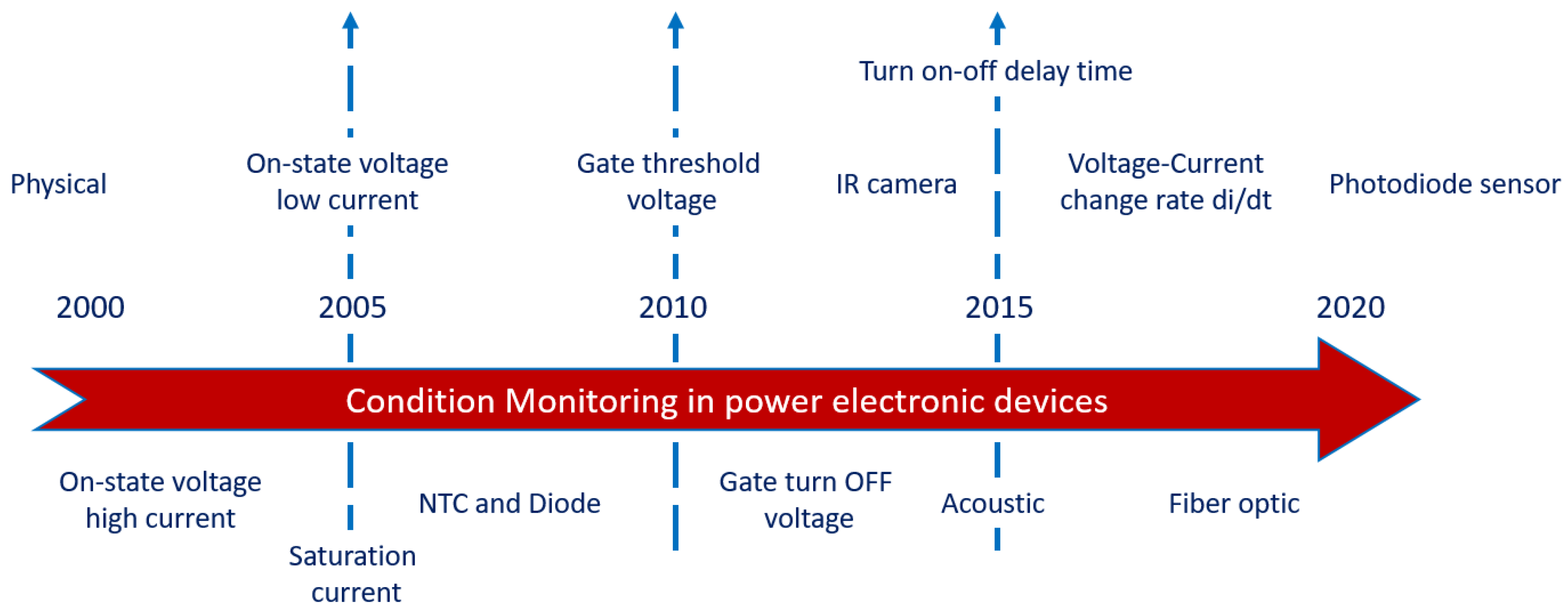
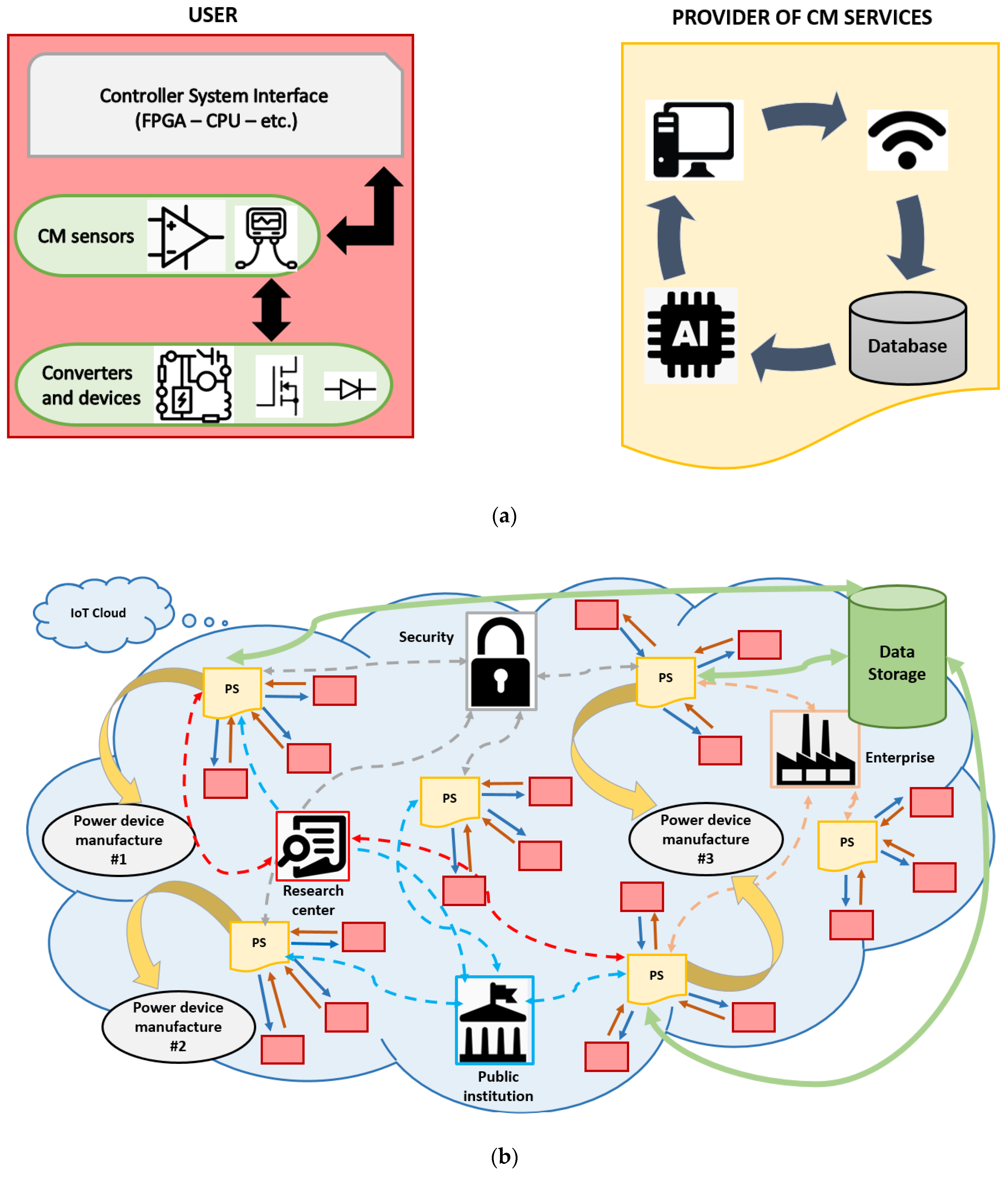
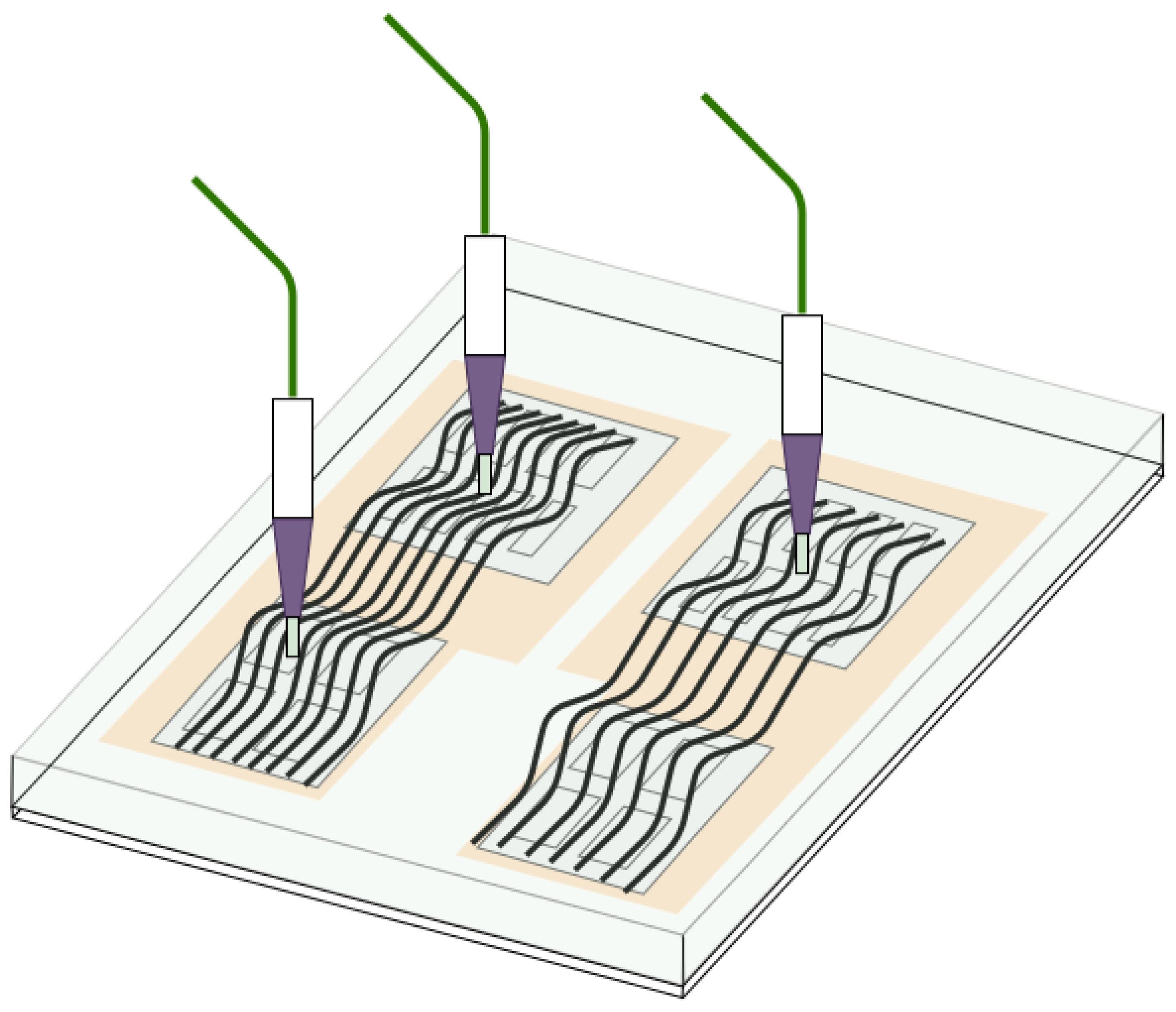
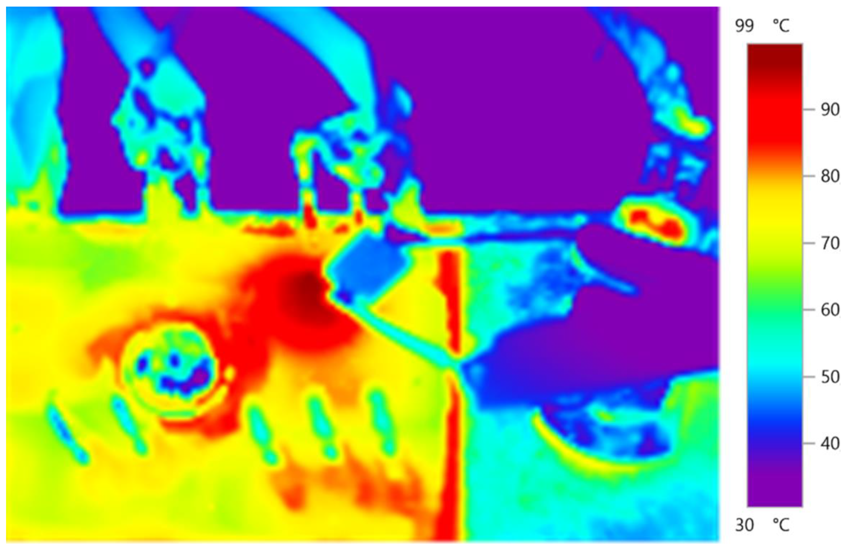
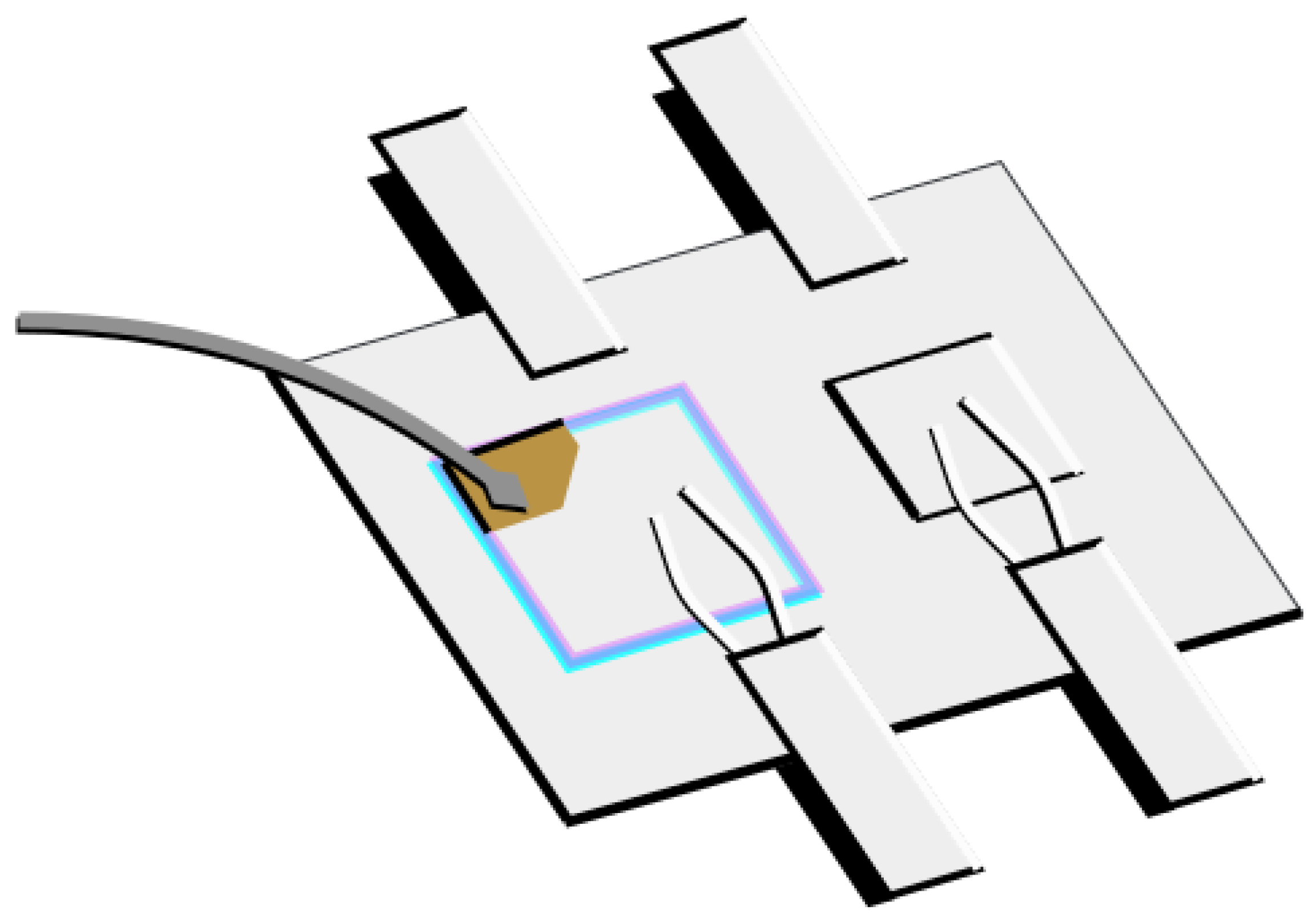
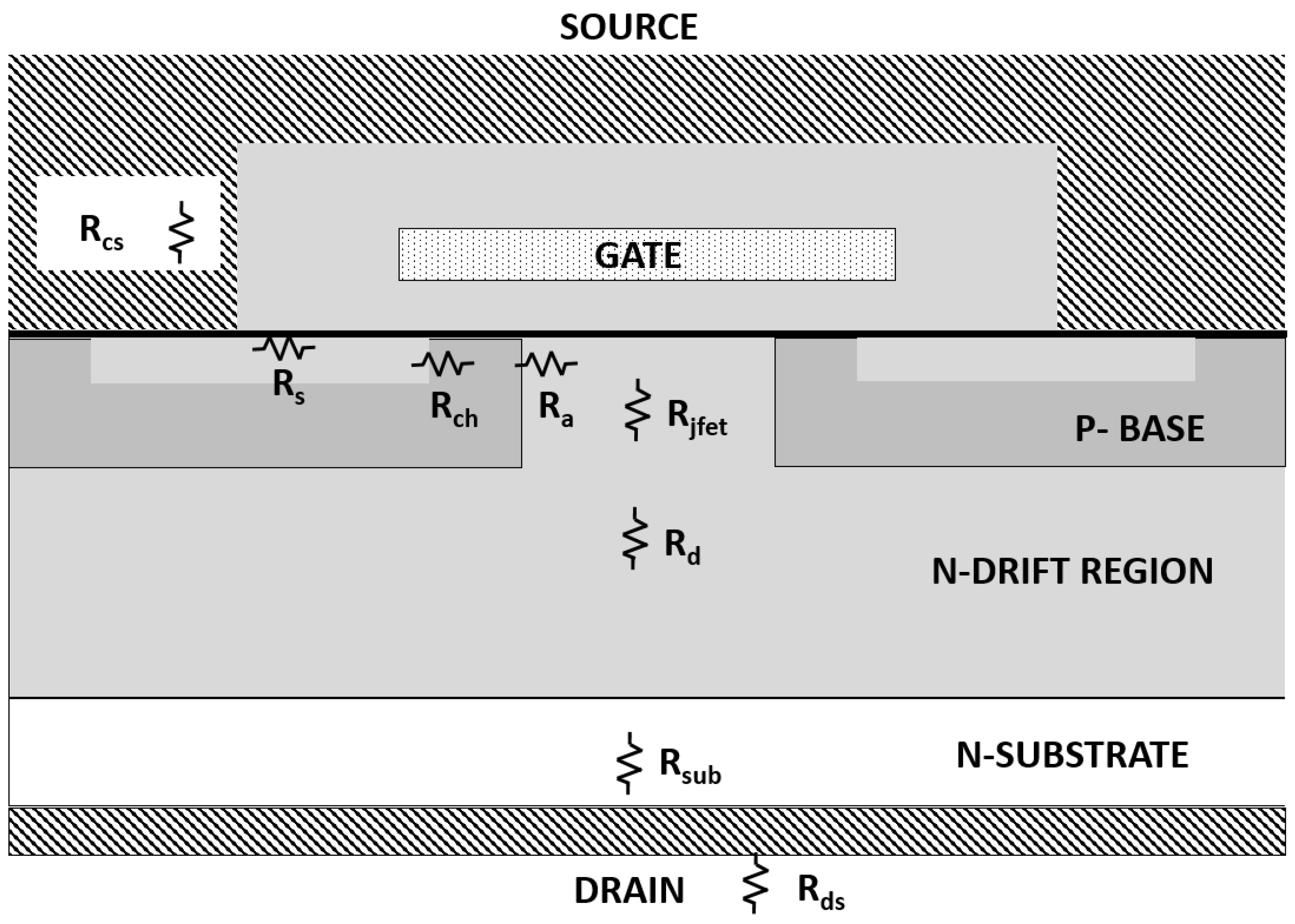
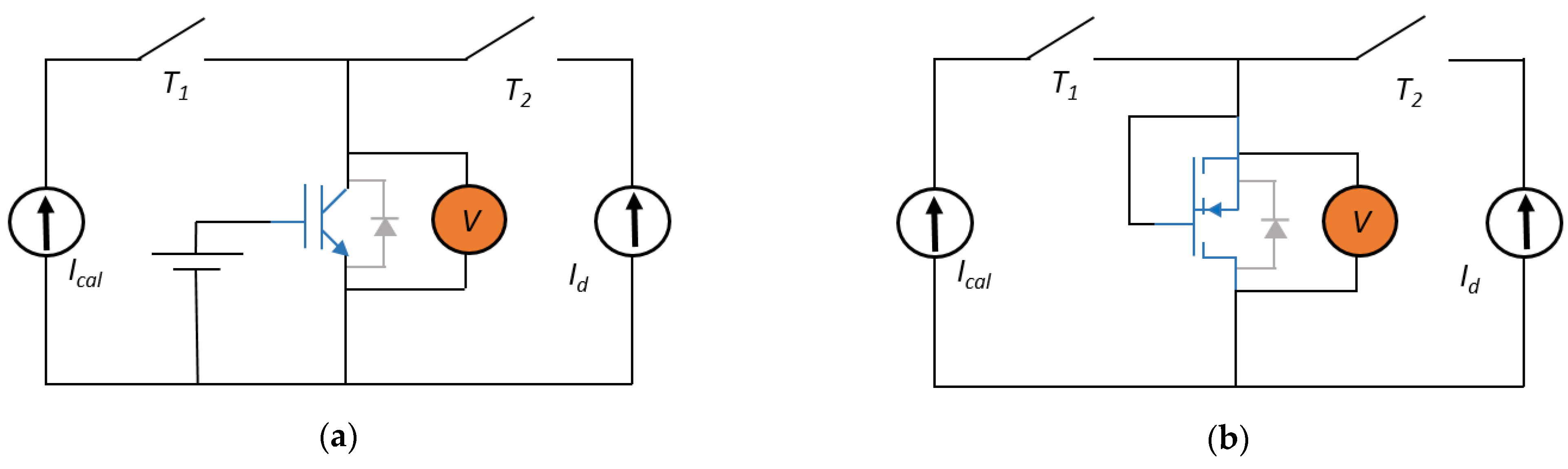
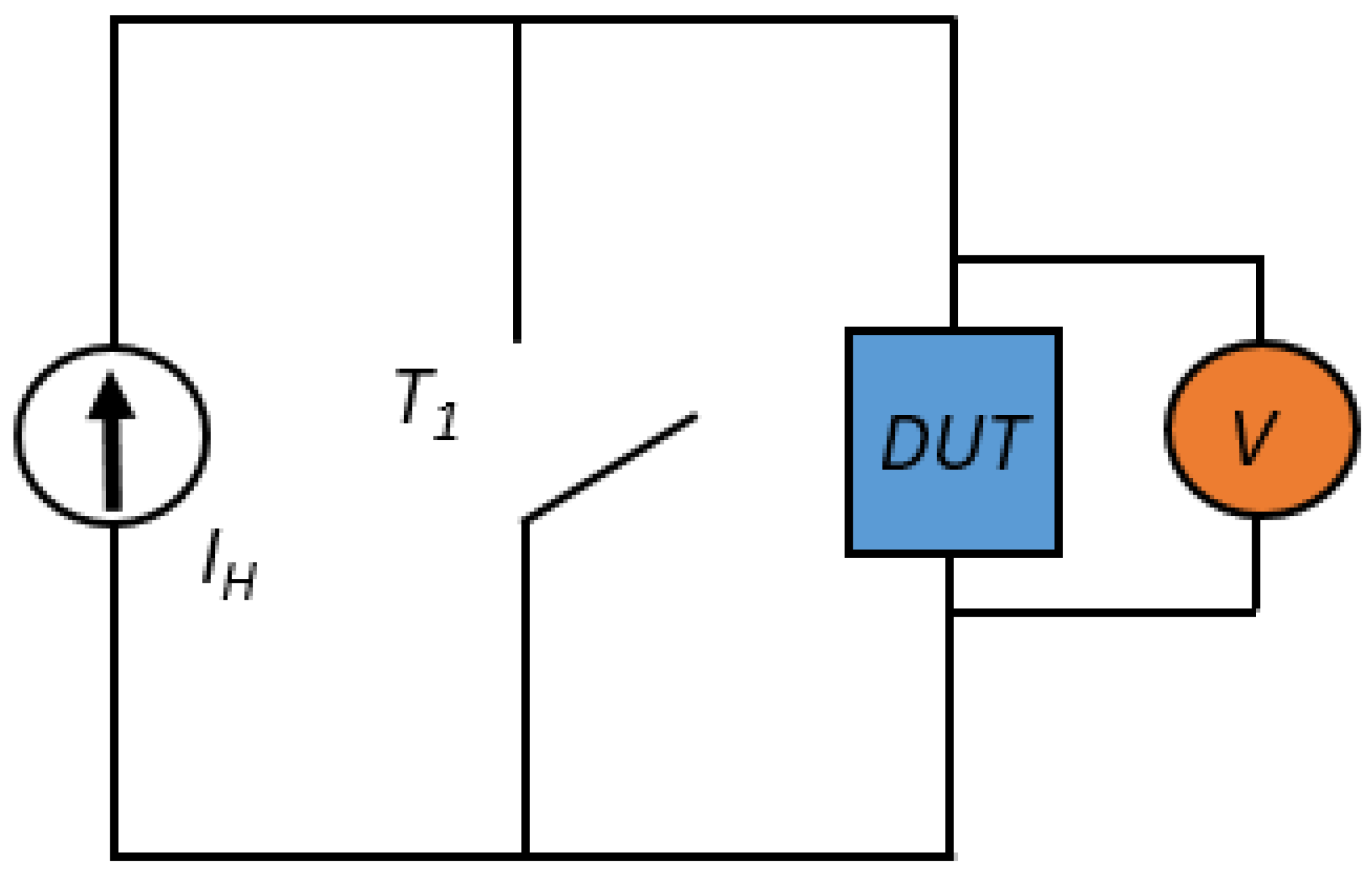
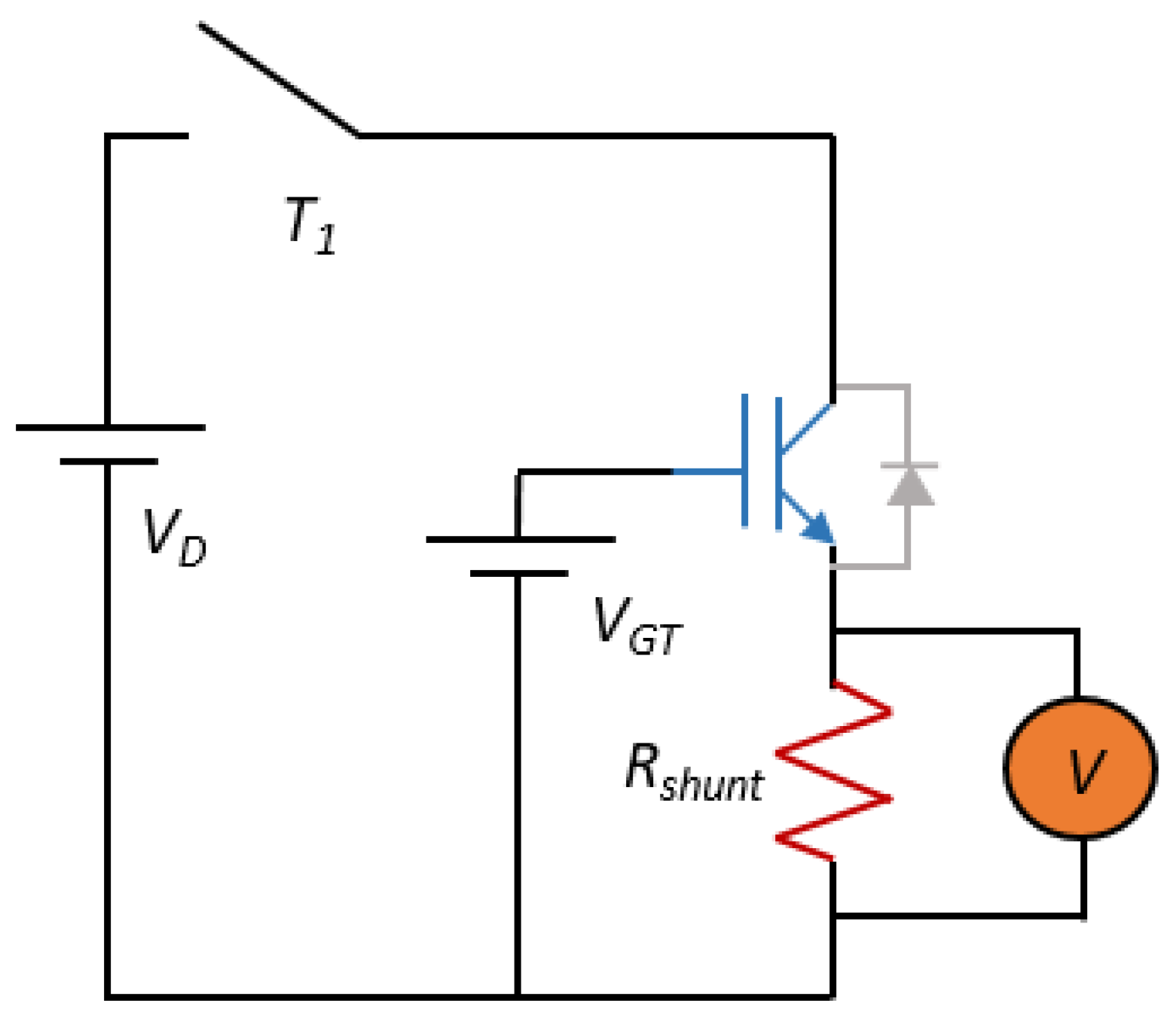
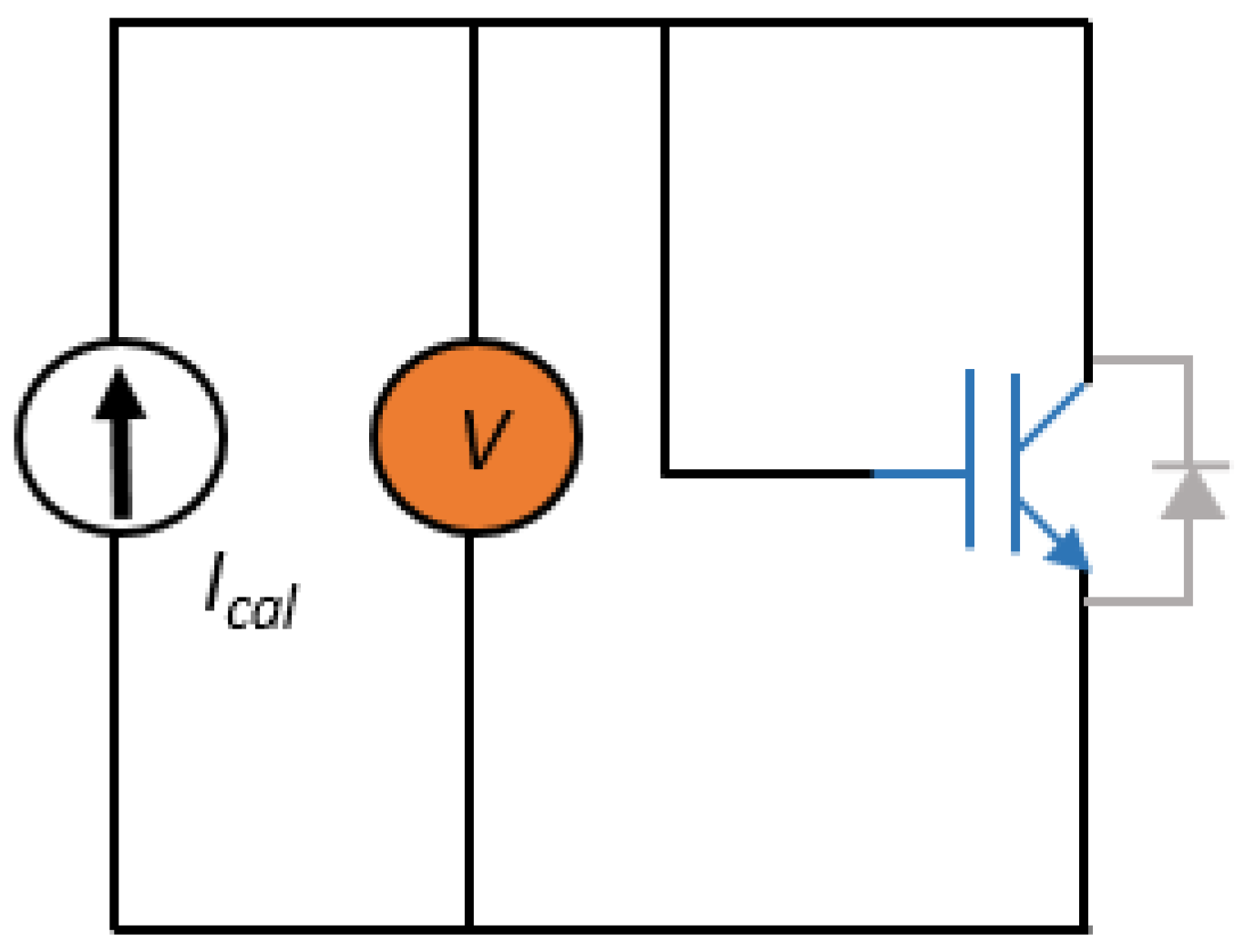
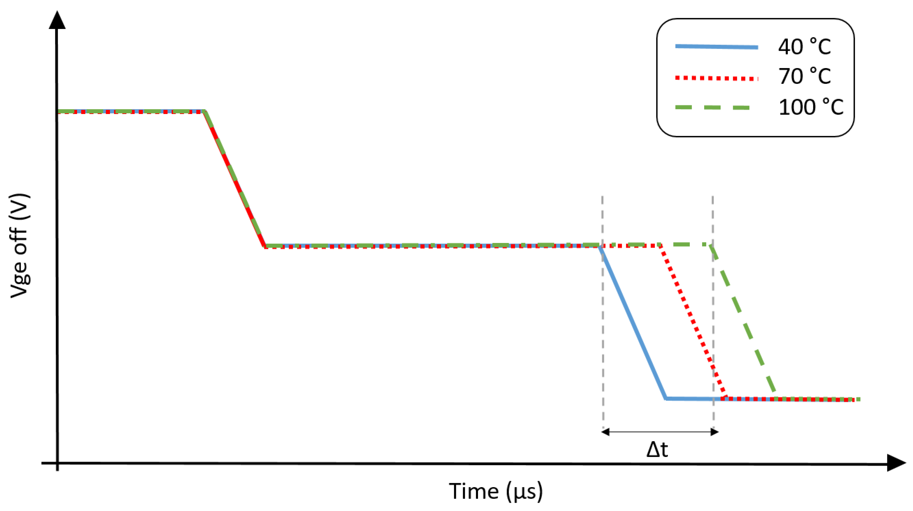
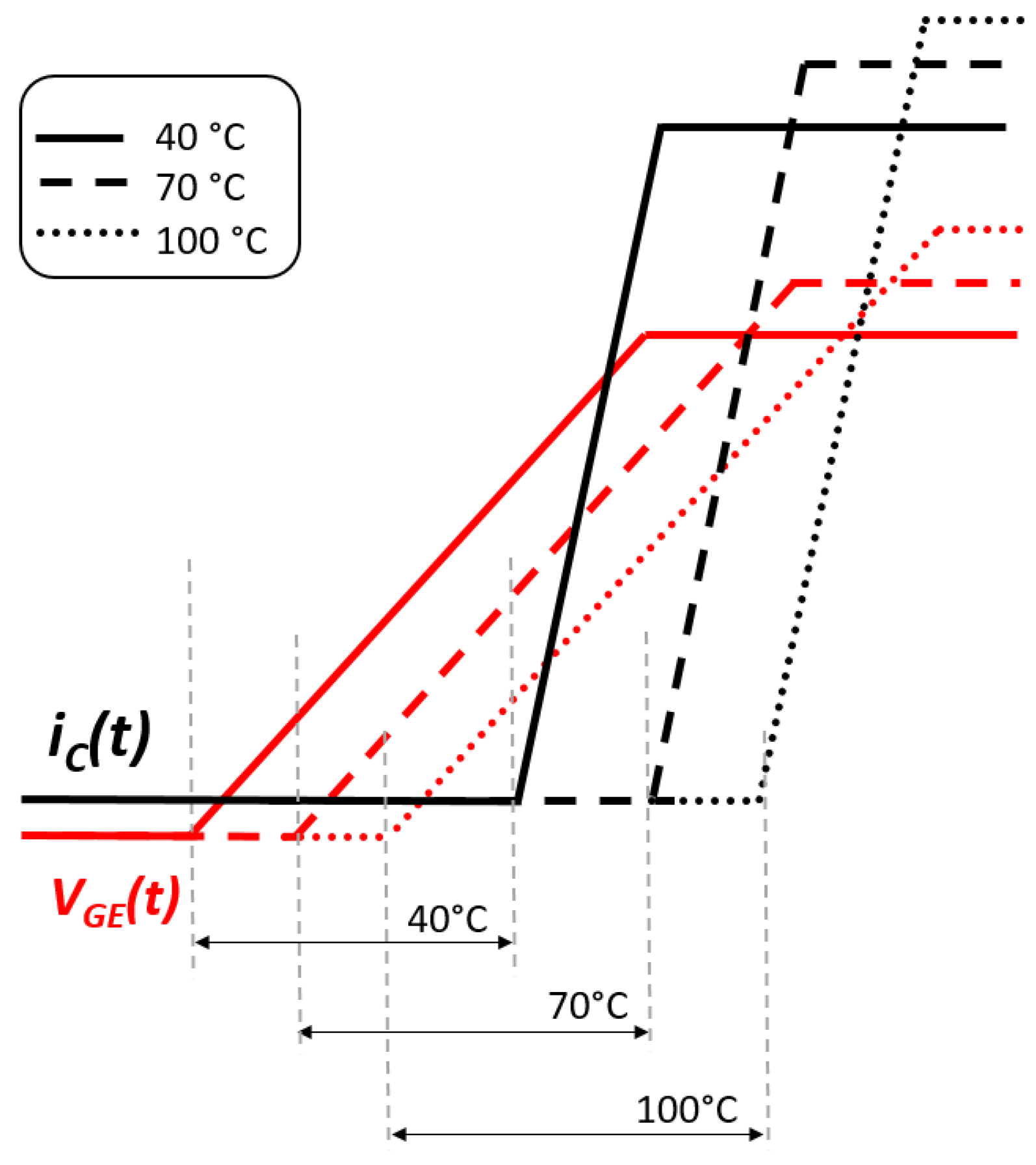
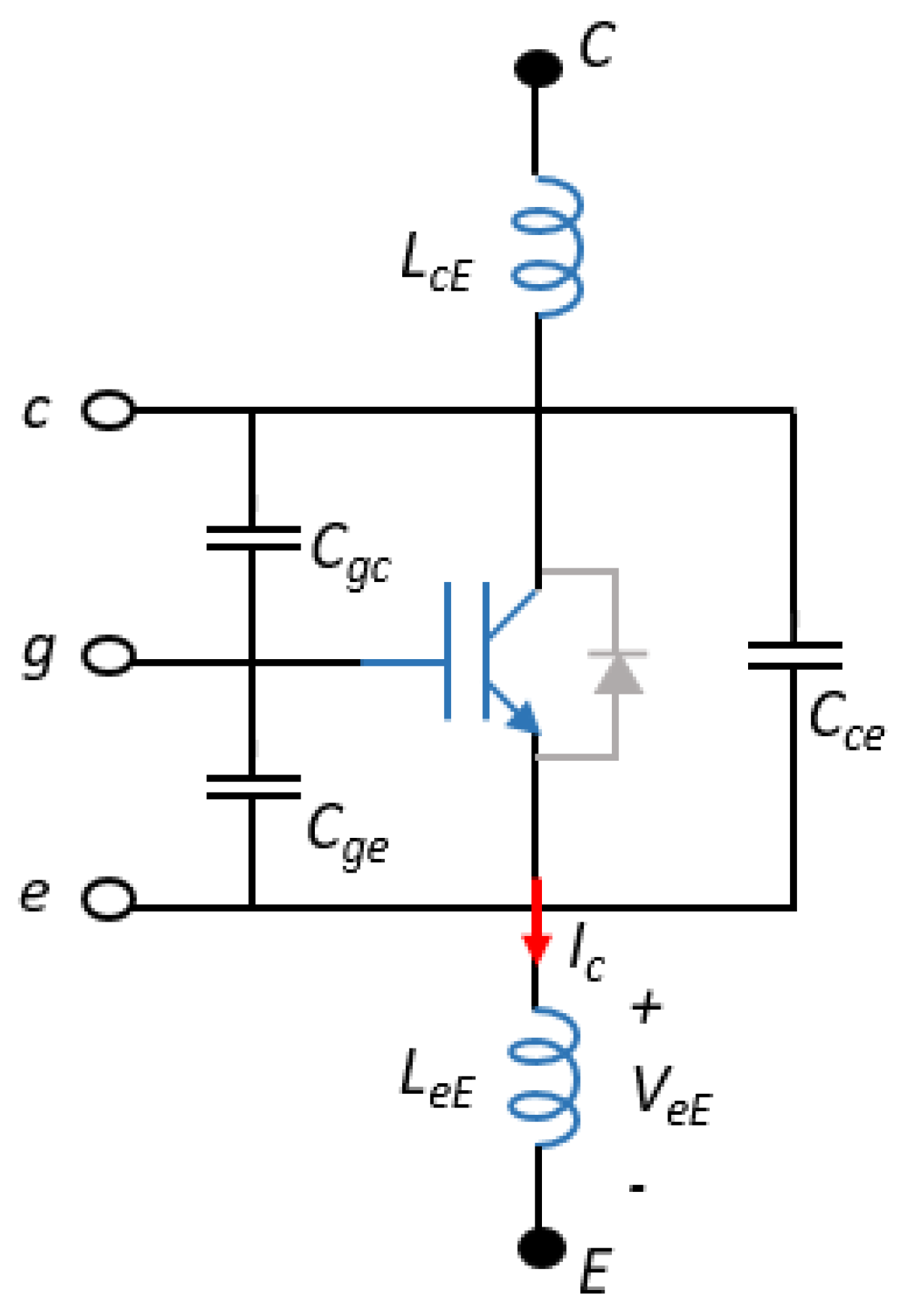
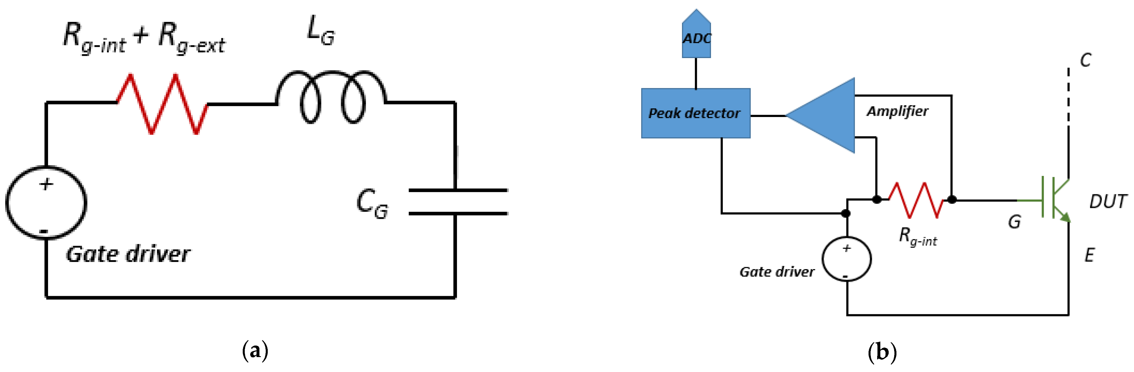
Table 1.
Measured quantities for the different condition monitoring (CM) methods. IR, infrared; NTC, negative temperature coefficient; TTC, thermal test chip; TSEP, thermo-sensitive electrical parameter.
Table 1.
Measured quantities for the different condition monitoring (CM) methods. IR, infrared; NTC, negative temperature coefficient; TTC, thermal test chip; TSEP, thermo-sensitive electrical parameter.
| Method | Measured Quantity |
|---|---|
| Acoustic | Acoustic waves |
| OPTICAL—Fiber optic | Light wavelength |
| OPTICAL—Photodiode sensor—internal | Light intensity |
| OPTICAL—Photodiode sensor—external | Light intensity |
| OPTICAL—IR camera print | Light wavelength |
| OPTICAL—IR camera | Light wavelength |
| Physical | Resistance |
| TTCs—NTC | Resistance |
| TTCs—Diode | Voltage |
| TSEP—On-state voltage, low current | Vce, Vds |
| TSEP—On-state voltage, high current | Device current, Vce, Vds |
| TSEP—Saturation current | Vce–Vds |
| TSEP—Gate threshold voltage | Vge—Vgs |
| TSEP—Gate turn OFF voltage | Vge–Vce, Vgs–Vds, Gate resistance |
| TSEP—Turn on-off delay time | Device current, Vce–Vds |
| TSEP—Voltage–current change rate di/dt | Device current, Vce–Vds |
| TSEP—Peak gate current | Vge–Vgs |
Table 2.
Summary of different CM methods.
| Method | Advantages | Disadvantages |
|---|---|---|
| OPTICAL—Fiber optic [46,47,48] | On-line measurements High sensitivity and accuracy | Package modification High cost |
| OPTICAL—Photodiode sensor—internal | On-line measurements Contactless | Technology not mature Package modification |
| OPTICAL—Photodiode sensor—external [56,57,58] | On-line measurements Contactless | Package modification |
| OPTICAL—IR camera [48,49,50,51,52,53] | Spatial resolution Contactless | Package modification Poor response time Poor accuracy |
| OPTICAL—IR camera print [49] | Spatial resolution Contactless | Poor response time Poor accuracy |
| Acoustic [28,29,30,31,32,33] | On-line measurements Contactless | Technology not mature Noise sensitive |
| Physical [59,60,61,62,63,64,65] | On-line measurements High linearity and sensitivity | Package modification Poor response time |
| TTCs—NTC [67,69,70,72,75] | On-line measurements High linearity | Layout modification Aging sensitive |
| TTCs—Diode [68,71] | On-line measurements High sensitivity | Layout modification Poor linearity |
| TSEP—On-state voltage, low current [80,81,82,83,84,85,86,87,88,89,90,91,92,93,94,95] | High sensitivity, linearity Easy calibration | High-cost sensing Off-line measurements |
| TSEP—Gate threshold voltage [89,93,94,103,104,105] | High sensitivity and linearity | Off-line measurements Unplug DUT |
| TSEP—On-state voltage, high current [96,97,98,99] | On-line measurements High linearity | High-cost sensing Aging sensitive |
| TSEP—Saturation current [87,93,100,101] | High sensitivity | Off-line measurements Poor linearity |
| TSEP—Gate turn OFF voltage [108,109] | High linearity | Off-line measurements High-cost sensing |
| TSEP—Turn on-off delay time [110,111,112,113,114,115,116] | On-line measurements High linearity | Aging sensitive High-cost sensing |
| TSEP—Peak gate current [129,130] | On-line measurements High linearity | Aging sensitive High-cost sensing |
| TSEP—Voltage-current change rate [117,118,119,120,121] | High sensitivity and linearity | Off-line measurements Gate resistance dependence |
Publisher’s Note: MDPI stays neutral with regard to jurisdictional claims in published maps and institutional affiliations. |
© 2021 by the authors. Licensee MDPI, Basel, Switzerland. This article is an open access article distributed under the terms and conditions of the Creative Commons Attribution (CC BY) license (http://creativecommons.org/licenses/by/4.0/).
Share and Cite
MDPI and ACS Style
Susinni, G.; Rizzo, S.A.; Iannuzzo, F. Two Decades of Condition Monitoring Methods for Power Devices. Electronics 2021, 10, 683. https://doi.org/10.3390/electronics10060683
AMA Style
Susinni G, Rizzo SA, Iannuzzo F. Two Decades of Condition Monitoring Methods for Power Devices. Electronics. 2021; 10(6):683. https://doi.org/10.3390/electronics10060683
Chicago/Turabian StyleSusinni, Giovanni, Santi Agatino Rizzo, and Francesco Iannuzzo. 2021. "Two Decades of Condition Monitoring Methods for Power Devices" Electronics 10, no. 6: 683. https://doi.org/10.3390/electronics10060683
Note that from the first issue of 2016, this journal uses article numbers instead of page numbers. See further details here.