Article

Individually Switchable InGaN/GaN Nano-LED Arrays as Highly Resolved Illumination Engines

1
Department of Electronic Engineering, University of Rome “Tor Vergata”, 00133 Rome, Italy
2
Department of Electronic and Biomedical Engineering, Universitat de Barcelona, 08028 Barcelona, Spain
3
Institute of Semiconductor Technology, University of Technology Braunschweig, 38106 Braunschweig, Germany
4
Laboratory for Emerging Nanometrology LENA, 38106 Braunschweig, Germany
5
ISM-CNR, Via Fosso del Cavaliere 100, 00133 Rome, Italy
*
Author to whom correspondence should be addressed.
Current address: Department of Physics, University of Warsaw, 02-093 Warsaw, Poland.
Electronics 2021, 10(15), 1829; https://doi.org/10.3390/electronics10151829
Submission received: 28 May 2021 / Revised: 24 July 2021 / Accepted: 26 July 2021 / Published: 30 July 2021
(This article belongs to the Special Issue Nitride Semiconductors Revolution: Material, Devices and Applications)

Abstract

:
GaN-based light emitting diodes (LEDs) have been shown to effectively operate down to nanoscale dimensions, which allows further downscaling the chip-based LED display technology from micro- to nanoscale. This brings up the question of what resolution limit of the illumination pattern can be obtained. We show two different approaches to achieve individually switchable nano-LED arrays. We evaluated both designs in terms of near-field spot size and optical crosstalk between neighboring pixels by using finite difference time domain (FDTD) simulations. The numerical results were compared with the performance data from a fabricated nano-LED array. The outcome underlines the influence of geometry of the LED array and materials used in contact lines on the final illumination spot size and shape.

Graphical Abstract

1. Introduction

GaN exhibits relatively slow surface recombination velocities, which gives the ability to downscale GaN-based light emitting diode (LED) technology to the nanoscale. Emission of light was observed in fact for nanowire devices down to diameters of ∼100 nm [1,2,3,4]. This property of GaN opens the possibility to create chip-integrated, dense nano-LED arrays having spatial resolution that is significantly higher than today’s devices. Until now, the reported nano-LED arrays do not allow for individual control over the LEDs and are characterized by low pixel density [4,5]. Indeed, although even LEDs as small as 100 nm have been reported, the methods used to fabricate the matrices did not allow for straightforward individual addressing schemes. Fully functional LED arrays allowing for single pixel control use GaN LED stripes of widths down to 900 nm [6], or have pixel sizes rather in the micrometer range [7,8,9,10,11]. The lack of literature on individually addressable nano-LED arrays can be partially justified by the fact that they are not suitable for microdisplay technology, which is dominated by micro-LED arrays [12] mostly targeting TV, smartphones and augmented reality (AR)/virtual reality (VR) displays. In addition, nano-LED technology faces significant challenges in fabrication. Indeed, the nano-LED arrays operate below the Abbé’s diffraction limit, and single pixels no longer can be distinguished by an optical system. Nevertheless, nano-LED technology opens a new area of chip-based devices potentially operating in a super-resolution regime applicable in highly-resolved microscopy [13,14] or structured illumination systems for, e.g., mask-less lithography [1] or optogenetics [15]. Individually switchable pixels allow obtaining a large number of different illumination patterns of high contrast [11,16]. Moreover, the nanometer size of the LEDs offers the advantage of creating a nano-sized resolved illumination pattern without bulky optical components, as found in many of the current structured illumination technologies [17]. The possibility of fabrication of a highly resolved illumination display on a chip allows developing potentially cheaper, smaller and more robust devices, as recently presented in the case of integrated chip-based microscopes [13,14].
In this paper, we report optical simulation results of individually addressable nano-LED arrays. We compare different designs, emphasize their advantages and limitations and discuss possible applications and guidelines for further improvement. The paper is organized as follows. First, we briefly describe the design and numerical setup for devices under investigation. Then, we discuss their optical characteristics obtained by numerical simulations and compare the results with characteristics of a fabricated device. Finally, we discuss possible applications of the proposed structures.

2. System Design and Methodology

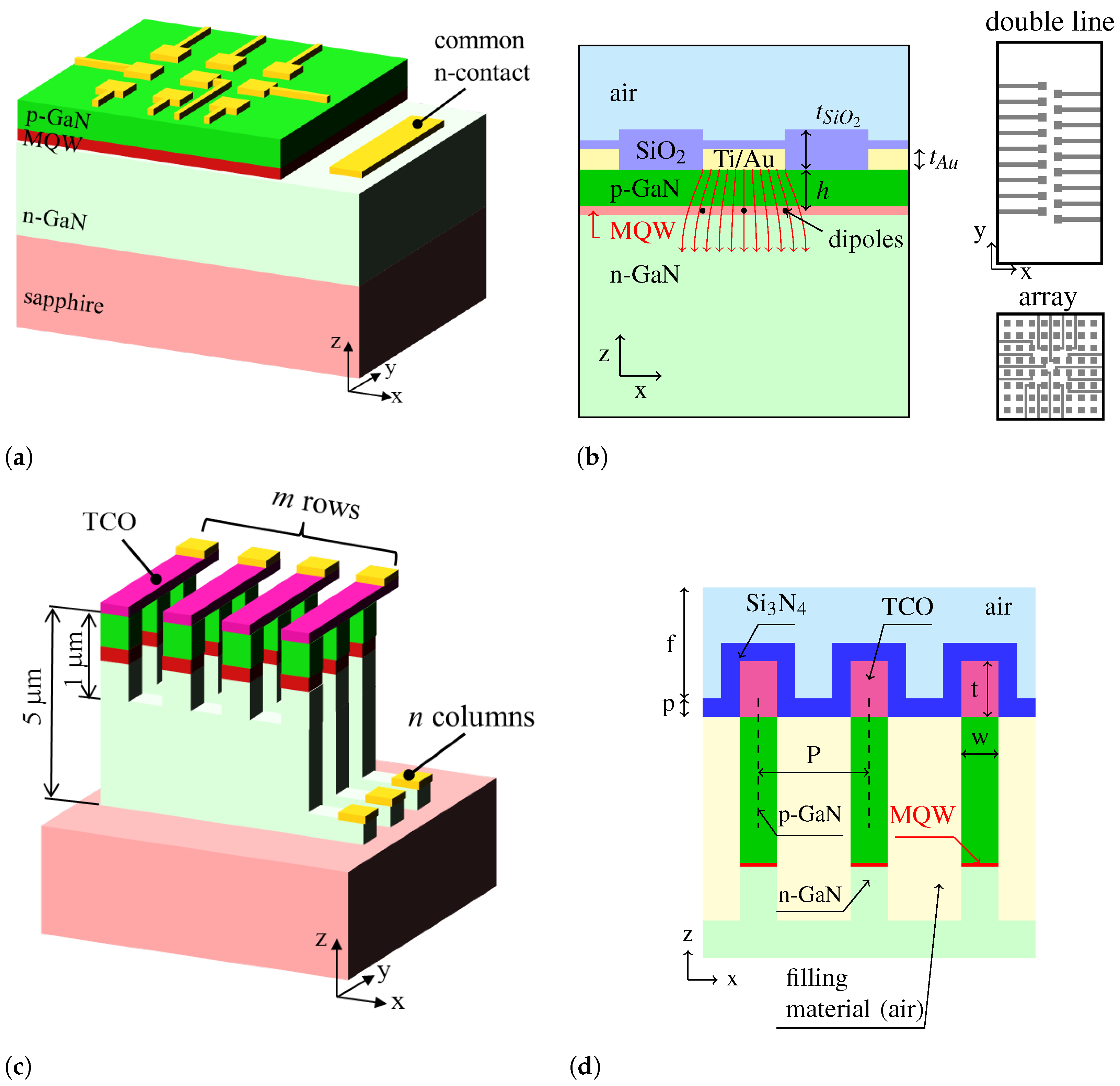
2.1. System Design Concepts

We investigated two technological concepts of nano-LED arrays. The main difference between the two is the method of accessing the individual pixels. In the first approach, which we denominate the direct addressing approach, every pixel can be addressed individually with a dedicated wire. In the second one, which we call the matrix addressing approach, the pixels are connected via orthogonal bottom and top contact lines, forming a passive LED matrix with addressing through columns and rows (see Figure 1). The direct addressing design overcomes the issue of the low conductivity of p-GaN, while, in the matrix addressing approach, the pixels are physically separated from each other by an etching process. The main advantage of the latter design is the possibility to scale up the number of the pixels in the array, which is not the case in the first approach. Indeed, the necessity to provide an individual contact line to every single LED, while avoiding crosstalk and short circuits on such a small scale, limits the number of pixels in the array. Until now, 6 × 6 pixel arrays with pixel size of 400 nm × 400 nm and a 2 × 32 pixel double line with pixel size of 200 nm × 200 nm have been fabricated, as described in [18]. It is worth noticing the half-pitch shift between the pixel positions in the two lines of the latter device, which has the potential to increase the spatial resolution. Note also that, in the direct addressing scheme, the pixel size is defined by the contact pad area, assuming that current spreading in the 100 nm thick p-GaN layer is small enough to not broaden the effective emission area. The matrix addressing concept requires electrical isolation between the different address lines, which can be implemented by a deep etching and subsequent planarization of the structure by filling with a suitable dielectric material; this is, however, difficult to perform and limits the size of the pixels in the latest fabricated arrays to above ∼1 μ m × 1 μ m [19]. For our simulations, we assumed air as the filling material, leading to a best case scenario. We also assumed an additional 3D structuring of the top 1 μ m of the LEDs by etching between the TCO top contact lines to help reduce optical crosstalk.

2.2. Numerical Model

We modeled the arrays using the commercial software CST Microwave studio (CST) [20]. CST is based on a general method to solve Maxwell’s equations known as the finite integration technique. The approach is implemented in both the time domain and the frequency domain and is not limited to one mesh type. An advantage of CST is its implementation of a meshing method called perfect boundary approximation, which allows for an accurate representation of curves and non-orthogonal features. A comparison of CST with different available software for specific problems are found in [21,22], while different solvers available in CST are discussed in [23]. For our calculations, we used the time domain solver, i.e., the finite difference time domain (FDTD) approach, since it requires less computational resources for optically large structures compared to other approaches.
Schematic figures of the different devices we studied are shown in Figure 1. In the case of directly addressed LEDs we studied two geometrical arrangements of the LEDs: the 8 × 8 array and two lines of pixels shifted by half of the period (see Figure 1b). For the matrix addressing scheme, we studied one configuration of an 11 × 11 LED array (see Figure 1c,d). The pixel size and period in all of the cases has been the same and equal to 200 nm × 200 nm and 400 nm, respectively. The distance between the active region, i.e., multi-quantum well layer (MQW), and the top surface of the LED is equal to 100 nm. As a source of the illumination, we used a set of nine point dipoles, placed on a grid with equal spacing covering the emitting area of the pixel. The emitting area was taken to be equal to the pixel size, meaning that in the direct addressing scheme we assumed negligible current spreading. The point dipoles were approximated by 5 nm long dipoles, using discrete ports in CST. We calculated and summed up the contributions from dipoles polarized in both x and y direction to properly model the unpolarized character of the light emission from the LED.
In order to avoid reflections on the boundaries of the numerical model, we used open boundary conditions on all domain boundaries. In order to limit spurious effects due to cutting the simulation domain, we used for the matrix addressing scheme at least 11 × 11 arrays, and did not use the results for the outermost pixels. In the direct addressing scheme, we added 800 nm of extra space around the pixel array. The optical properties of all of the materials were simulated using experimental dispersion data taken from literature and gathered in Table 1. The simulations were performed for a wavelength of λ = 450 nm, corresponding to a typical peak emission wavelength of blue InGaN/GaN LEDs. We used hexahedral mesh geometry assuring an optimized size of the mesh elements to minimize the error connected to inaccurate geometric representation and minimize the time of the calculations. Therefore, we used multiple mesh sizes for different material domains taking into account the value of dielectric function and domain size. We used at least five elements per wavelength or three elements per domain width. The suitability of the mesh was checked by performing a mesh convergence study. For a more detailed analysis of the matrix addressing structure, we refer to the work of Kluczyk-Korch et al. [14].

3. Results

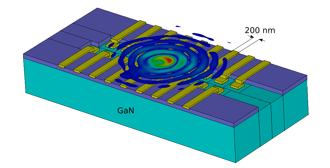
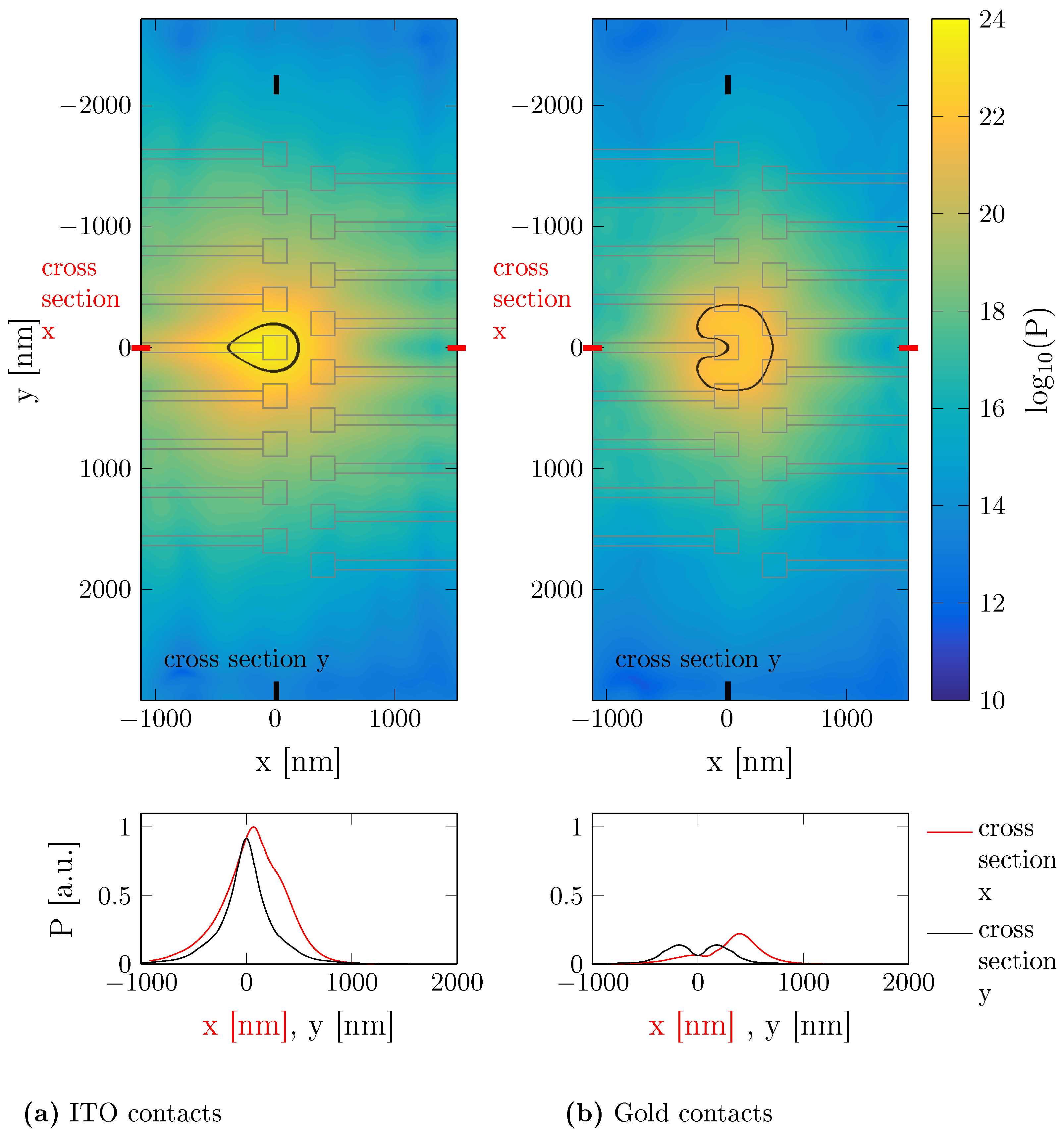
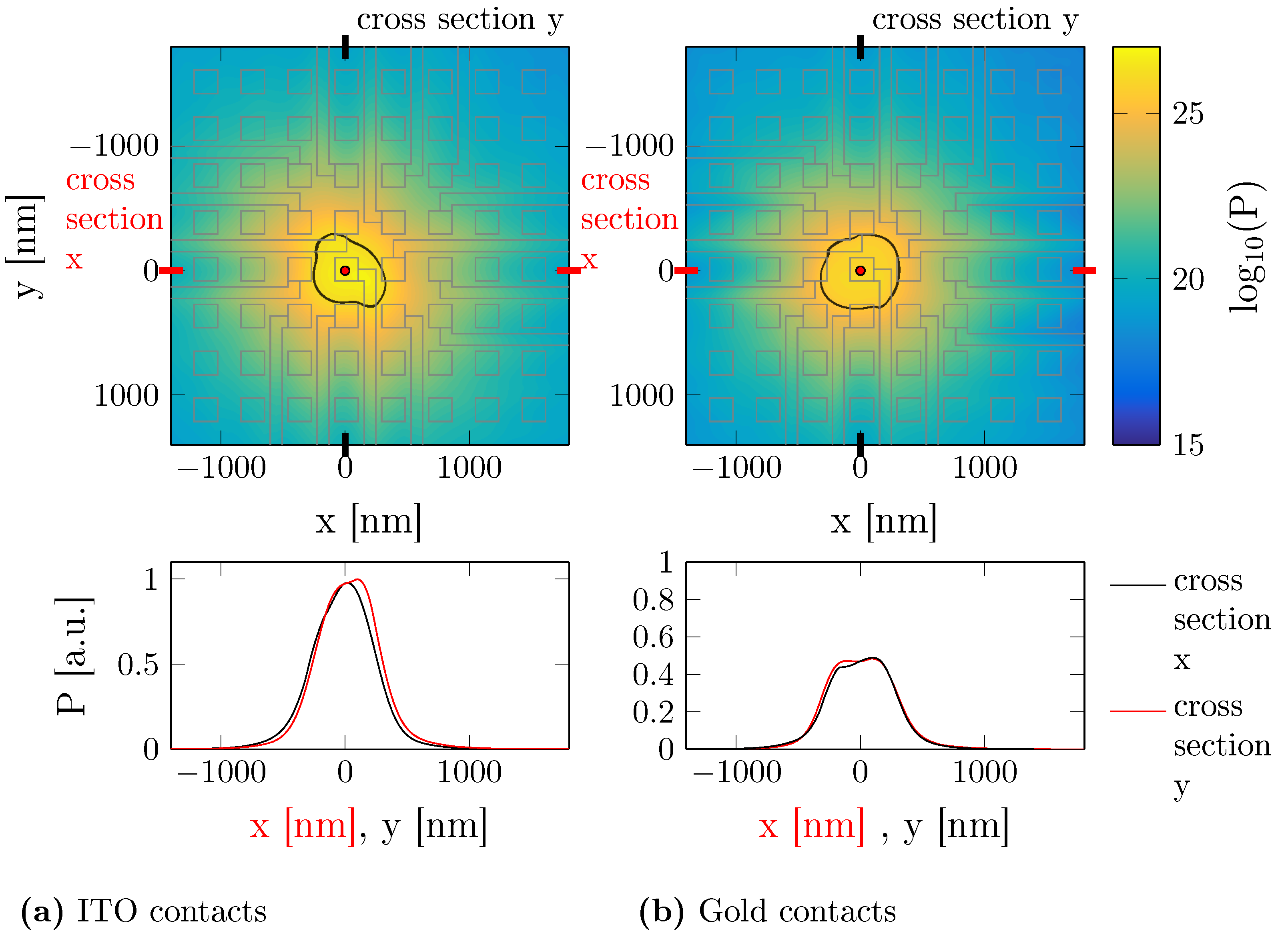
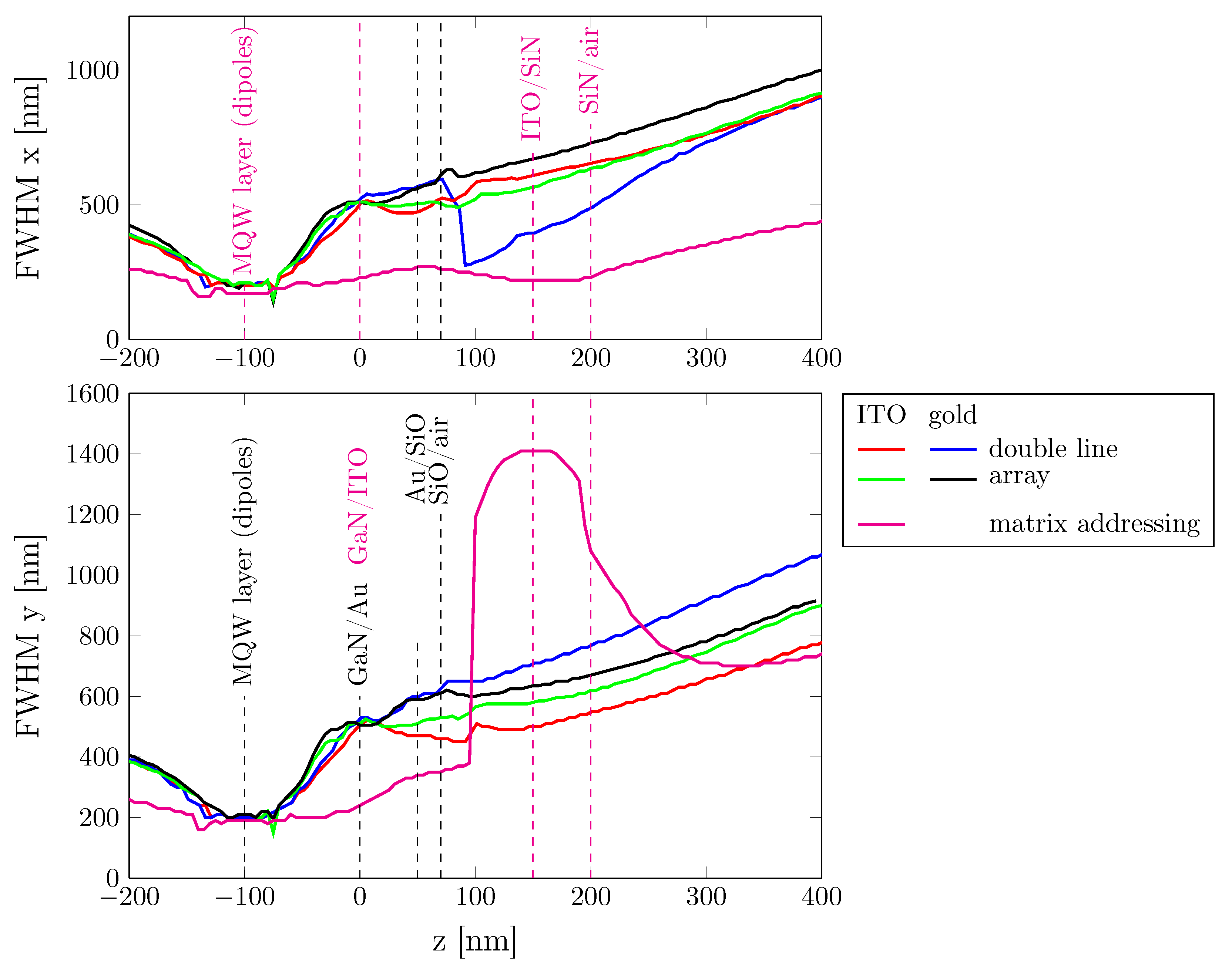
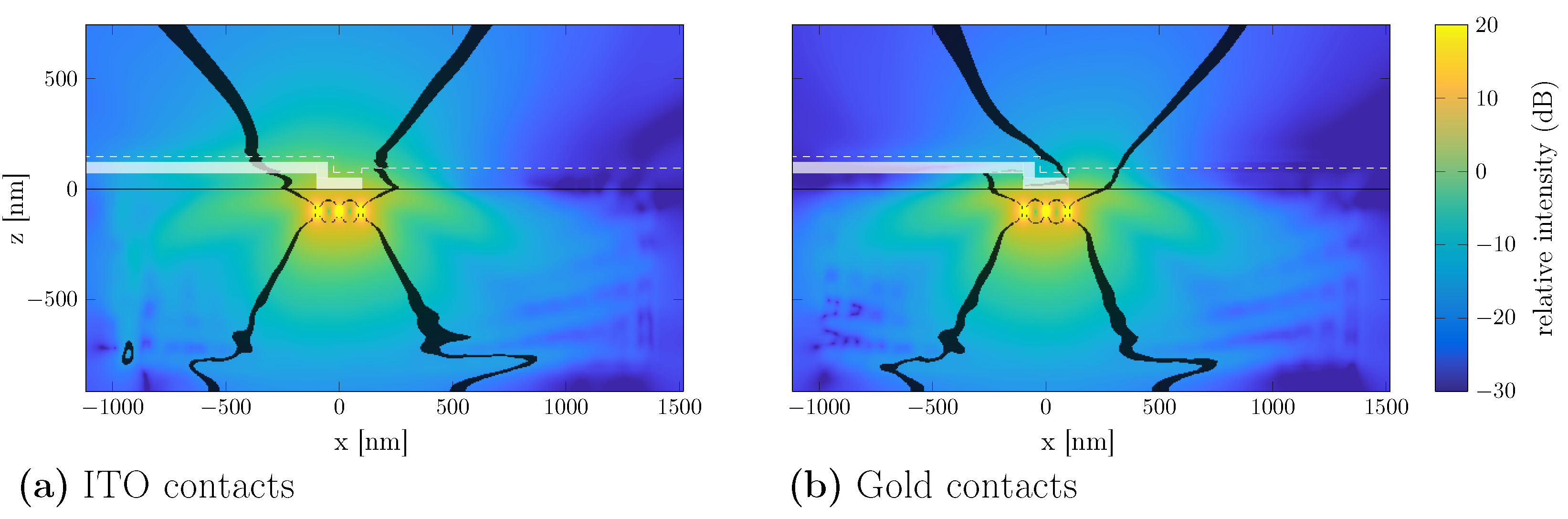
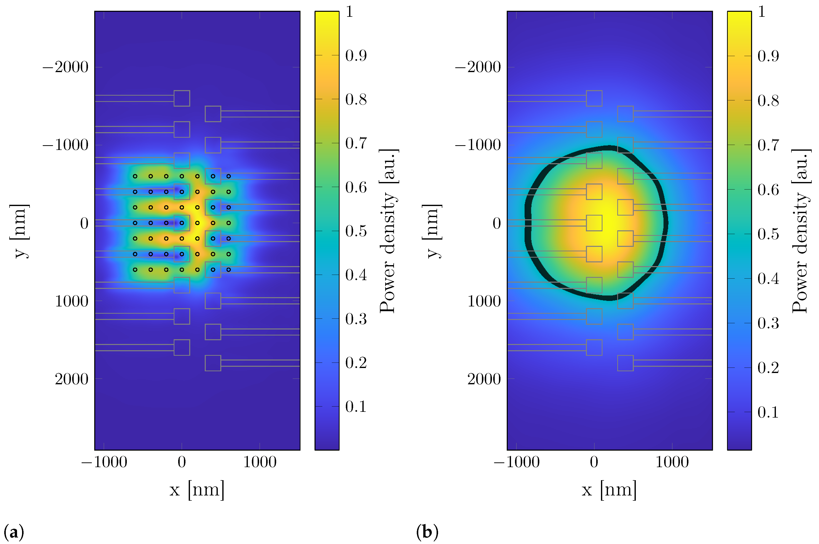
3.1. Near Field Distributions

We started the characterization of the optical properties of the devices from calculating the electromagnetic near field due to excitation of a single pixel of the array. As the distance of the active multi-quantum well layer in the GaN wafer is fixed by the technological process, the most important parameter, when the matrix is directly addressed, is the top contact material. We compared here gold contacts with contacts made of a transparent conductive oxide (TCO) such as indium tin oxide (ITO), which has higher optical transparency in comparison to a thin Ti/Au stack. In all cases, the contact metallization area corresponds to the nominal pixel area of 200 × 200 nm 2 . In the case of the matrix addressed LED array, there are much more parameters defining device geometry. However, in this paper, we restrict ourselves only to a matrix having the same geometry in terms of pixel size and period as the direct addressing matrix array. A detailed analysis of the impact of the array geometry on optical properties in the case of the matrix addressed scheme can be found in [14].
Figure 2 and Figure 3 compare the electromagnetic field power distribution for ITO and gold contacts on a plane placed 100 nm above the top surface of the array for the directly addressed double-line and array designs. The black lines denote the power density equal to half of its maximal value and the gray lines indicate the contact metallizations. We observe a significant difference in the shape, size and intensity of the light spot emitted from the LED in the case of the double-line design for the two contact materials. In the array design, we observe less difference. The reduction in the peak optical intensity in the case of gold contact compared to ITO is up to 80% for the double-line design and up to 50% for the matrix design. The difference in the shape and intensity can be explained by higher light absorption coefficient in the gold. Indeed, the intensity of the signal is reduced mostly in correspondence of the gold contacts. The less prominent difference in the spot shape for the matrix design can be related to the more symmetric arrangement of the top metallization. However, there is a visible plateau in the electromagnetic power intensity in correspondence to the location of the gold pad (see Figure 3).
Figure 4 shows the full width at half maximum (FWHM) of the light spot as a function of the position along the normal axis z. We compare the direct addressing LED arrays with the matrix addressed one. The size of the LED and the array period is the same for all devices and equal to 200 nm × 200 nm and 400 nm, respectively. The dashed lines indicate the positions of the different material interfaces in the LED structure, with black lines referring to direct-addressing LED arrays and the magenta lines to the matrix-addressed array.
In the case of the more symmetric matrix design, ITO contacts result in a more regular and smaller FWHM compared to gold contacts. At the top SiO 2 /air surface, the FWHM reduces from ∼630 to 530 nm. However, if we consider the double-line design, we observe a significant difference in the FWHM along the x and y axis, due to the contact wires’ orientation along the x direction. The increased absorption in gold leads to a smaller FWHM in x direction (along the wire) for the gold contact. However, it has to be emphasized that the FWHM values in Figure 4 are taken along the x and y axes going through the center of the LED, where the width of the light spot along x for the double-line design with gold contacts is minimal (see Figure 2). In fact, the sudden reduction of the FWHM in correspondence of the surface can be identified with the blocking effect of the gold contact, as seen in the intensity distribution on the xz pane (taken at the center of the pixel) shown in Figure 5. On the other hand, the FWHM in y direction is again reduced when using ITO contacts (in this case from 650 to 520 nm).
Comparing the FWHM for direct addressing and matrix addressing schemes, the latter represented by the magenta lines in Figure 4, we notice a substantial difference. The matrix addressing structure exhibits a large elongation of the intensity distribution along the ITO crossbars (with x y ratio ∼0.18 at the ITO/Si 3 N 4 interface). This is due to guiding of the light along the ITO crossbars. As a result, the FWHM in x direction for the matrix addressing device is significantly smaller and in y direction significantly larger than that in the direct addressing structure, regardless of the contact material. Please notice that the comparison has to be made at the top surface of the LED arrays, i.e., at the SiO 2 /air interface for direct addressing systems and at the Si 3 N 4 /air interface for matrix addressing system.

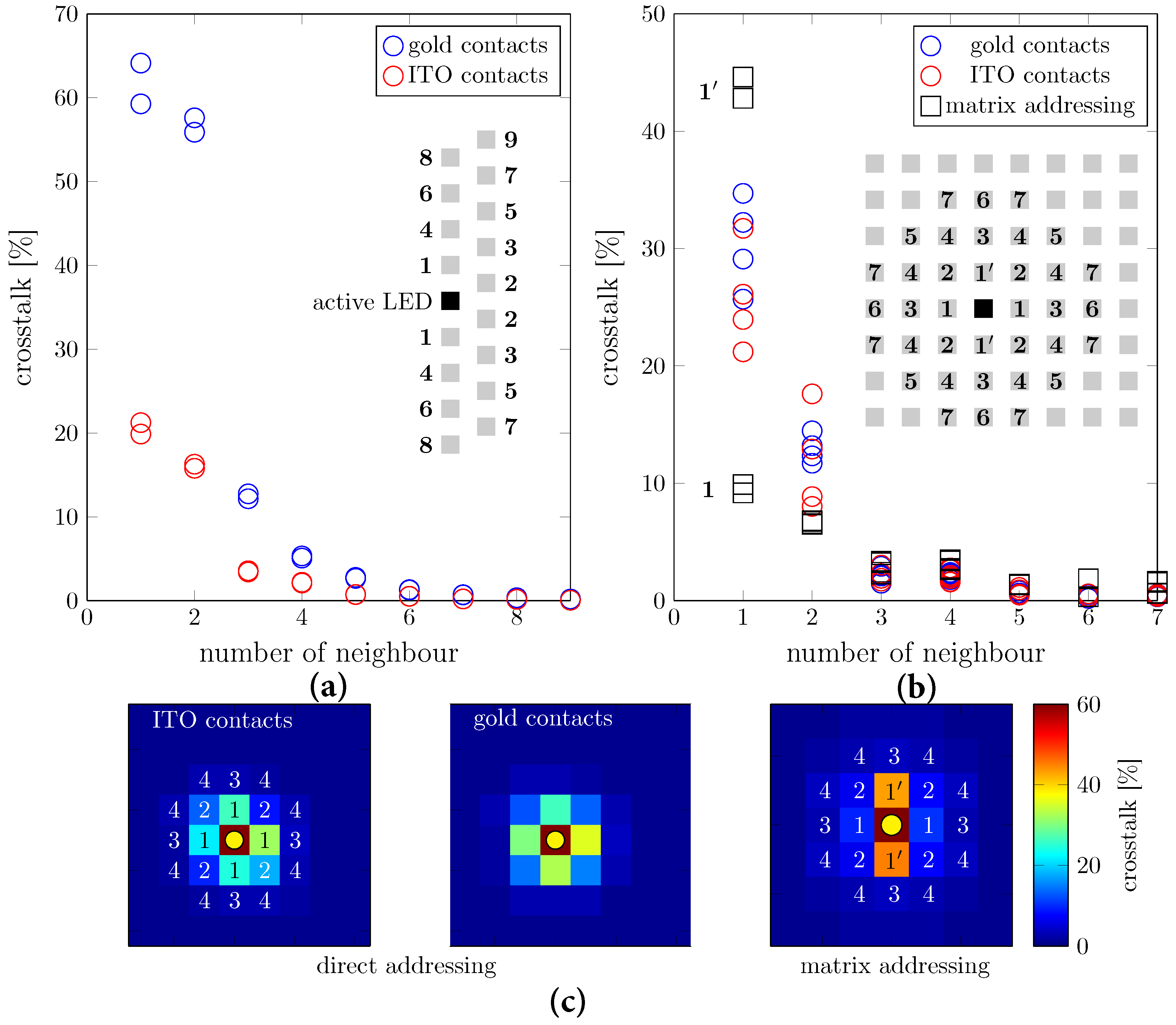
3.2. Optical Crosstalk between the Pixels

One of the crucial parameters defining the overall performance of a display system is the crosstalk between the neighboring pixels. This parameter was investigated for the studied systems in order to optimize the device design. Here, we focus on the optical crosstalk, but it is important to emphasize that there can be other sources of crosstalk, e.g., the electrical one. In the proposed structures, electrical crosstalk is limited due to the small conductivity of p-GaN or the 3D-patterning. In the case of the direct addressing approach, current spreading is small enough to assume that the area of light emission is equal to the p-contact area, which thus defines the pixel size [18]. Optical crosstalk in the studied structures is related to light propagating from the emitting pixel to other pixels, directly or via reflections, and leading to light intensity in the object plane in correspondence of non-activated pixels. This is unwanted, since in the targeted applications the intensity distribution in the object plane should relate to the activated pixels.
We define the optical crosstalk between two LEDs indicated by indices i and j as [28]
c i , j ( % ) = P i , j P j × 100 % ,
where P i , j is the power emitted by the ith LED and propagating through the surface of jth LED and P j is the power emitted by jth LED and propagating through the surface of jth LED. Figure 6 shows the optical crosstalk between the pixels in the direct and matrix addressing LED arrays. The change of contact material from gold to ITO considerably reduces the crosstalk in the double-line design from ∼62% down to ∼20% for the closest neighbors. The effect is more subtle in the case of the matrix geometry. Comparison between direct and matrix addressing approaches reveals significantly larger crosstalk for the nearest-neighbor pixels along y direction (along the ITO crossbars) in the latter case. We associate this with a significant dispersion of the light emission along the ITO crossbars, visible in Figure 4 as a steep increase of FWHM at the ITO/Si 3 N 4 interface. Indeed, by looking at the map of crosstalk between pixels (see Figure 6c) we notice a directional spread of the signal with larger crosstalk along direction of the ITO crossbars. For the direct addressing arrays, we observe only small deviation from a homogeneous spread. Interestingly, the crosstalk to second nearest pixels is larger in the case of direct addressing arrays, because the periodic dielectric structure in the xy plane induced by the 3D patterning in the matrix-addressed structure partly suppresses in-plane light propagation.
A pronounced anisotropy can be observed in all cases. This is due to the fact that the simulated structures lack symmetry. The direct addressing structures are not symmetric with respect to reflection at the xz or yz plane, while the matrix addressing scheme is structurally different in x and y directions. Therefore, crosstalk to neighbors along the two directions is different. Note, however, that, e.g., in the double line design, the difference depends also on how many pixels are included in the simulation.
The large crosstalk along the ITO contact lines in case of the matrix addressing scheme could presumably be reduced by a careful optimization of the top contact and passivation layers. Note, however, that in a real structure a filling material with refractive index > 1 probably needs to be employed, which reduces index contrast and therefore potentially decreases electromagnetic field confinement, leading to larger crosstalk.

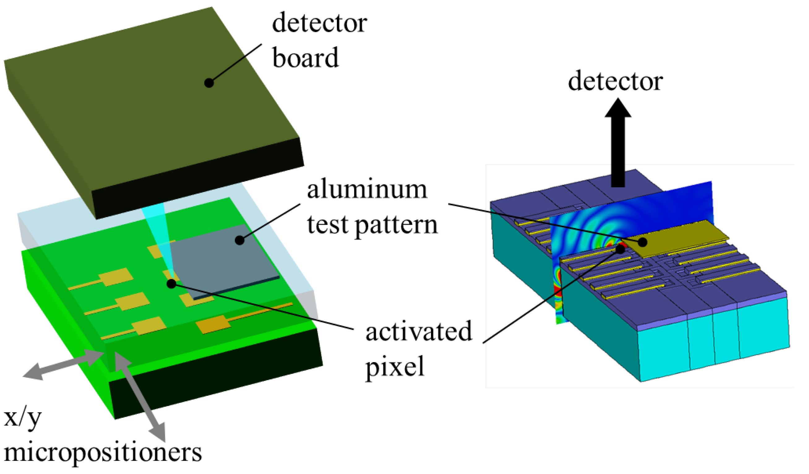
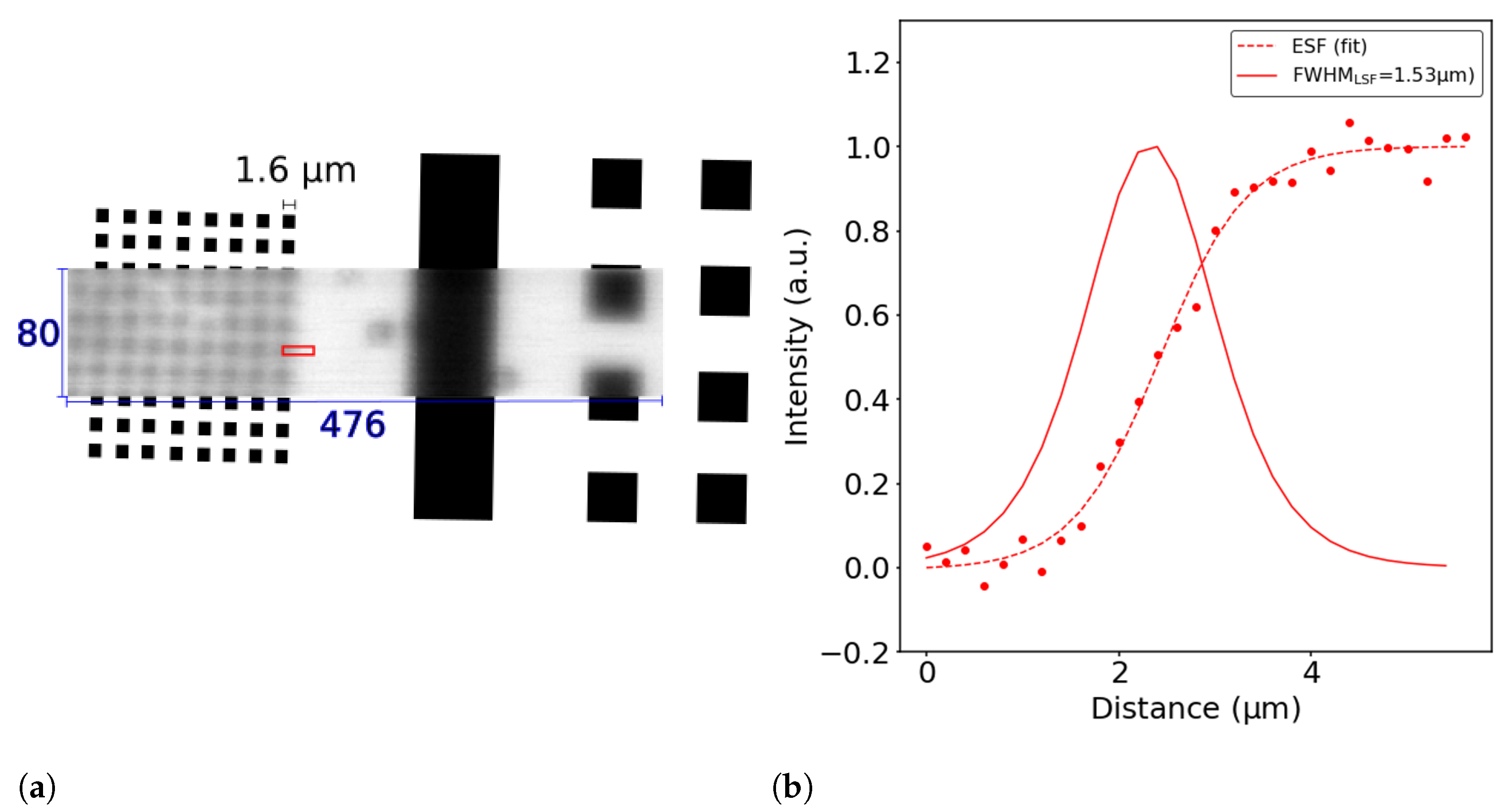
3.3. Experimental Results

In order to validate the simulation results and experimentally determine the effective spatial dimension of the light spot produced by the LEDs, shadow images of a metallic test pattern defined by electron-beam lithography (EBL) were acquired and analyzed by extracting the edge spread function (ESF). For this purpose, a custom scanning microscope was built, using the 2 × 32 direct addressing double-line nano-LED as illumination engine. The metallic pattern made of aluminum consisted in rectangular patterns of different dimensions with sharp edges, deposited on glass. This pattern was then placed directly onto the LED chip, with the metallized side facing the LEDs. A single LED has been activated with a constant bias current of 800 nA, and a shadow image with 80 × 476 pixels was acquired by moving the glass carrier with the metal pattern along x and y with steps of 200 nm using micropositioners, therefore covering an area of 16 × 95.2 μ m 2 . The transmitted light was detected using a monochrome 1/3-Inch wide-VGA CMOS digital image sensor with 6 μ m pixels (MT9V024 from On Semiconductor, Phoenix, AZ, USA). The setup is shown schematically in Figure 7, with the LED array on the bottom, the test pattern (in the figure a single metallic square) in the middle and the detector board on top. Details on the microscope can be found in [29,30].
The shadow image reconstructed from the measured intensities for each positioning of the test pattern is shown in Figure 8a as a blurry rectangle in gray scale. The metal pattern that was used in the experiment is shown in the same figure in black. It can be observed that the edges in the experimental shadow image are not sharp. This gradual transition from light to dark is described by the ESF, which can be extracted from the measured intensities, and is shown in Figure 8b as symbols. Here, we extracted the ESF from the area indicated by the red rectangle in Figure 8a, corresponding to the edge of the smaller 1.6 × 1.6 μ m 2 mask features.
By means of the ESF, it is possible to determine the spatial resolution of the system [31], which in our case is directly related to the light spot size in the plane of the metallic mask. In fact, we assume that the FWHM of the light spot in the direction normal to the illuminated metal edge corresponds to the FWHM of the line spread function (LSF), which is the derivative of the ESF, shown in Figure 8b by the red curve. We estimated the FWHM from the measured data, resulting in a value of ∼1.53 μ m.
The experimentally determined FWHM is considerably larger than the one theoretically predicted from the spot size, which is around 500–700 nm. The discrepancy can be explained in two ways. On the one hand, the exact distance of the illuminated pattern from the top surface of the LED array is not precisely known, so that the relevant spot size might be larger than that just at the interface. From the results in Figure 4, we can estimate that this would require a distance of ∼600 nm, which however seems unrealistic as the glass slide with the metal pattern has been put directly on top of the LED chip. On the other hand, in the simulations, we assumed negligible current spreading in the p-GaN layer. However, some amount of current spreading might be expected in the p-GaN contact layer or in MQW layer itself. To reach the measured FWHM, the emitting area would have to be roughly on the order of 1 μ m in diameter. A qualitative view of a spot resulting from an extended emission area is shown in Figure 9, modeled via an array of 7 × 7 dipoles centered at the active pixel. A comparison with the measured FWHM thus indicates that current spreading or diffusion in the MQW region reaches at most the nearest or second nearest pixels in the given geometry.

4. Conclusions

We present the results of numerical simulations of individually addressable nano-LED arrays on a chip based on GaN technology. The comparison of different structural designs showed the importance of the top contact geometry on the optical crosstalk between the neighboring pixels and resulting FWHM of the light spot. Interestingly, the shape of the illumination spot depends not only on the structure of the LED but also on the spatial arrangement of pixels and contacts. Optical crosstalk between the closest pixels is on the order of several tens of percent, but it can be reduced to ∼20% by changing the contact material and increasing its optical transparency, employing for example a transparent conductive oxide such as ITO instead of gold. The smallest FWHM, obtained at the top surface of the LED array, is predicted for the double-line nano-LED array using direct addressing approach and is equal to ∼600 nm. However, measurements suggest that current spreading may play an important role in LEDs of such dimensions, so that it is difficult to reach the theoretical value without suitable 3D patterning. Nevertheless, the successful fabrication and integration of the nano-LED arrays into a microscope confirms the possibility of applications of this technology in future designs.

Author Contributions

Conceptualization, A.W. and A.D.; methodology, K.K.-K., M.A.d.M. and A.D.; simulations, K.K.-K.; validation, M.A.d.M., A.D.C. and A.D.; formal analysis, K.K.-K., S.M. and J.C.; investigation, K.K.-K., S.M. and J.C.; resources, A.D., A.D.C., A.W.; data curation, K.K.-K., S.M. and J.C.; sample preparation J.G., J.H., writing—original draft preparation, K.K.-K.; writing—review and editing, M.A.d.M., A.D.C., A.D., A.W. and J.G.; visualization, K.K.-K., S.M. and J.C.; supervision, M.A.d.M.; project administration, A.D., A.W. and A.D.C.; funding acquisition, A.D., A.W. and A.D.C. All authors have read and agreed to the published version of the manuscript.

Funding

This research was funded by the European Union’s Horizon 2020 research and innovation program under grant agreement No. 737089; by the Deutsche Forschungsgemeinschaft (DFG, German Research Foundation) under Germany’s Excellence Strategy—EXC-2123 QuantumFrontiers—390837967; by the Deutsche Forschungsgemeinschaft (DFG, German Research Foundation) under Germany’s Excellence Strategy within the Cluster of Excellence PhoenixD (EXC2122, Project ID 390833453).

Conflicts of Interest

The authors declare no conflict of interest.

References

  1. Mikulics, M.; Hardtdegen, H. Nano-LED array fabrication suitable for future single photon lithography. Nanotechnology 2015, 26, 185302. [Google Scholar] [CrossRef]
  2. Mikulics, M.; Arango, Y.; Winden, A.; Adam, R.; Hardtdegen, A.; Grützmacher, D.; Plinski, E.; Gregušová, D.; Novák, J.; Kordoš, P.; et al. Direct electro-optical pumping for hybrid CdSe nanocrystal/III-nitride based nano-lightemitting diodes. Appl. Phys. Lett. 2016, 108, 061107. [Google Scholar] [CrossRef] [Green Version]
  3. Mikulics, M.; Winden, A.; Marso, M.; Moonshiram, A.; Lüth, H.; Grützmacher, D.; Hardtdegen, H. Nano-light-emitting-diodes based on InGaN mesoscopic structures for energy saving optoelectronics. Appl. Phys. Lett. 2016, 109, 041103. [Google Scholar] [CrossRef]
  4. Mariana, S.; Gülink, J.; Handmana, G.; Yu, F.; Strempel, K.; Spende, H.; Yulianto, N.; Granz, T.; Prades, J.; Peiner, E.; et al. Vertical GaN Nanowires and Nanoscale Light-Emitting-Diode Arrays for Lighting and Sensing Applications. ACS Appl. Nano Mater. 2019, 2, 4133–4142. [Google Scholar] [CrossRef]
  5. Mikulics, M.; Sofer, Z.; Winden, A.; Trellenkamp, S.; Förster, B.; Mayer, J.; Hardtdegen, H. Nano-LED induced chemical reactions for structuring processes. Nanoscale Adv. 2020, 2, 5421–5427. [Google Scholar] [CrossRef]
  6. Gong, Z.; Guilhabert, B.; Chen, Z.; Dawson, M. Direct LED writing of submicron resist patterns: Towards the fabrication of individually-addressable InGaN submicron stripe-shaped LED arrays. Nano Res. 2014, 7, 1849–1860. [Google Scholar] [CrossRef] [Green Version]
  7. Day, J.; Li, J.; Lie, D.; Bradford, C.; Lin, J.; Jiang, H. III-Nitride full-scale high-resolution microdisplays. Appl. Phys. Lett. 2011, 99, 031116. [Google Scholar] [CrossRef]
  8. Templier, F. GaN-based emissive microdisplays: A very promising technology for compact,ultra-high brightness display systems. J. Soc. Inf. Disp. 2016, 24, 669–675. [Google Scholar] [CrossRef]
  9. Herrnsdorf, J.; Jonathan, J.D.; McKendry, J.; Zhang, S.; Xie, E.; Ferreira, R.; Massoubre, D.; Zuhdi, A.; Henderson, R.; Underwood, I.; et al. Active-Matrix GaN Micro Light-Emitting DiodeDisplay With Unprecedented Brightness. IEEE Trans. Electron Device 2015, 62, 1918–1925. [Google Scholar] [CrossRef] [Green Version]
  10. Kishino, K.; Sakakibara, N.; Narita, K.; Oto, T. Two-dimensional multicolor (RGBY) integrated nanocolumn micro-LEDs as afundamental technology of micro-LED display. Appl. Phys. Express 2020, 13, 014003. [Google Scholar] [CrossRef]
  11. Griffiths, A.; Herrnsdorf, J.; McKendry, J.; Strain, M.; Dawson, M. Gallium nitride micro-light-emitting diode structured light sources for multi-modal optical wireless communications systems. Philos. Trans. R. Soc. A 2020, 378. [Google Scholar] [CrossRef] [PubMed] [Green Version]
  12. Wu, Y.; Ma, J.; Su, P.; Zhang, L.; Xia, B. Full-Color Realization of Micro-LED Displays. Nanomaterials 2020, 12, 2482. [Google Scholar] [CrossRef]
  13. Franch, N.; Canals, J.; Moro, V.; Villá, A.; Romano-Rodríguez, A.; Prades, J.D.; Gülink, J.; Bezdhlyakh, D.; Waag, A.; Kluczyk-Korch, K.; et al. Nano-Illumination Microscopy: A technique based on scanning with an array of individually addressable nanoLEDs. Opt. Express 2020, 28, 19044–19057. [Google Scholar] [CrossRef]
  14. Kluczyk-Korch, K.; Palazzo, D.; Waag, A.; Diéguez, A.; Prades, J.; Di Carlo, A.; Auf der Maur, M. Optical design of InGaN/GaN nanoLED arrays on a chip: Toward: Highly resolved illumination. Nanotechnology 2020, 32, 105203. [Google Scholar] [CrossRef]
  15. McAlinden, N.; Massoubre, D.; Richardson, E.; Gu, E.; Sakata, S.; Dawson, M.; Mathieson, K. Thermal and optical characterization of micro-LED probes for in vivo optogenetic neural stimulation. Opt. Lett. 2013, 38, 992–994. [Google Scholar] [CrossRef] [PubMed] [Green Version]
  16. Moreno, I. Image-like illumination with LED arrays: Design. Opt. Lett. 2012, 37, 839–841. [Google Scholar] [CrossRef]
  17. Křížek, P.; Raška, I.; Hagen, G. Flexible structured illumination microscope with a programmable illumination array. Opt. Express 2012, 20, 24585–24599. [Google Scholar] [CrossRef]
  18. Bezshlyakh, D.; Spende, H.; Weimann, T.; Hinze, P.; Bornemann, S.; Gülink, S.; Canals, J.; Prades, J.; Diégez, A.; Waag, A. Directly addressable GaN-based nanoLED arrays: Fabrication and electro-optical characterization. Microsyst. Nanoeng. 2020, 6, 88. [Google Scholar] [CrossRef]
  19. Gülink, J.; Bornemann, S.; Spende, H.; Auf der Maur, M.; Di Carlo, A.; Prades, J.D.; Wasisto, H.S.; Waag, A. InGaN/GaN nanoLED Arrays as a Novel Illumination Source for Biomedical Imaging and Sensing Applications. Proceedings 2018, 2, 892. [Google Scholar] [CrossRef] [Green Version]
  20. Dassault Systèmes. CST Studio Suite. 2019. Available online: https://www.3ds.com (accessed on 22 October 2019).
  21. Hirtenfelder, F. Effective Antenna Simulations using CST MICROWAVE STUDIO®. In Proceedings of the 2007 2nd International ITG Conference on Antennas, Munich, Germany, 28–30 March 2007; p. 239. [Google Scholar] [CrossRef]
  22. Kozlov, M.; Turner, R. A comparison of ansoft HFSS and CST microwave studio simulation software for multi-channel coil design and SAR estimation at 7T MRI. Piers Online 2010, 6, 395–399. [Google Scholar] [CrossRef]
  23. Demming-Janssen, F.; Koch, W. 3D Field simulation of sparse arrays using various solver techniques within CST MICROWAVE STUDIO®. In Proceedings of the 2006 European Radar Conference, Manchester, UK, 13–15 September 2006; pp. 80–83. [Google Scholar] [CrossRef]
  24. Kawashima, T.; Yoshikawa, H.; Adachi, S. Optical properties of hexagonal GaN. J. Appl. Phys. 1997, 82, 3528–3535. [Google Scholar] [CrossRef]
  25. Johnson, P.; Christy, R. Optical Constants of The Noble Metals. Phys. Rev. B 1972, 6, 4370–4379. [Google Scholar] [CrossRef]
  26. König, T.A.F.; Ledin, P.A.; Kerszulis, J.; Mahmoud, M.A.; El-Sayed, M.A.; Reynolds, J.R.; Tsukruk, V.V. Electrically Tunable Plasmonic Behavior of Nanocube-Polymer Nanomaterials Induced by a RedoxActive Electrochromic Polymer. ACS Nano 2014, 8, 6182–6192. [Google Scholar] [CrossRef] [PubMed]
  27. Rodríguez-de Marcos, L.; Larruquert, J.; Méndez, J.; Aznárez, J. Self-consistent optical constants of SiO2 and Ta2O5 films. Opt. Mater. Express 2016, 6, 3622–3637. [Google Scholar] [CrossRef]
  28. Woods, A. Crosstalk in stereoscopic displays: A review. J. Electron. Imaging 2012, 21, 040902. [Google Scholar] [CrossRef]
  29. Canals, J.; Franch, N.; Moro, V.; Moreno, S.; Prades, J.D.; Romano-Rodríguez, A.; Bornemann, S.; Bezshlyakh, D.D.; Waag, A.; Vogelbacher, F.; et al. A Novel Approach for a Chip-Sized Scanning Optical Microscope. Micromachines 2021, 12, 527. [Google Scholar] [CrossRef]
  30. Moreno, S.; Canals, J.; Moro, V.; Franch, N.; Vilà, A.; Romano-Rodriguez, A.; Prades, J.D.; Bezshlyakh, D.D.; Waag, A.; Kluczyk-Korch, K.; et al. Pursuing the Diffraction Limit with Nano-LED Scanning Transmission Optical Microscopy. Sensors 2021, 21, 3305. [Google Scholar] [CrossRef]
  31. Viallefont-Robinet, F.; Helder, D.; Fraisse, R.; Newbury, A.; van den Bergh, F.; Lee, D.; Saunier, S. Comparison of MTF measurements using edge method: Towards reference data set. Opt. Express 2018, 26, 33625–33648. [Google Scholar] [CrossRef] [PubMed]
Figure 1. Scheme of the proposed nano-LED arrays. (a) The direct addressing scheme. Here, every pixel has its own p-side contact line (yellow), while the n-side contact is shared. A cross section is shown in (b), where the SiO2 passivation layers are also indicated. Several point dipole sources are distributed over the emitting pixel area. The latter is determined by the current flow, indicated by the red arrows. We assume negligible in-plane current spreading. The two layouts studied in this work are depicted on the right. (c) The matrix addressing scheme. Here, a deep etching step completely isolates the different LED columns, while orthogonal p-side contact lines made from transparent conductive oxide (TCO) are used for addressing the rows, resulting in an m × n array. A cross section in the xz plane is shown in (d), indicating some of the structural parameters. The top 1 μm of the structure is etched also between the TCO p-side contacts, for increased optical isolation. The size of the pixels and pitch of the arrays used in the modeling was the same for all designs and equals 200 × 200 nm2 and 400 nm, respectively. The remaining parameters are the distance from source dipole to top surface of GaN h = 100 nm, thickness of Ti/Au contact tAu = 50 nm, thickness of SiO2 layer tSiO2 = 95 nm, thickness of TCO crossbars t = 150 nm and thickness of Si3N4 layer p = 50 nm.
Electronics 10 01829 g001
Figure 2. Logarithm of the electromagnetic field intensity in the xy plane for the directly addressed double-line design, 100 nm above the top surface of the LEDs. The black lines indicate the iso-intensity curves at half of the maximal value. The gray lines show the alignment of LEDs and corresponding contacts. (a) Intensity distribution for ITO contacts. (b) Intensity distribution for gold contacts. The plots in bottom row show the intensity along the x (red) and y (black) cross sections through the center of the activated LED. The values are normalized to the maximum obtained for ITO contacts.
Electronics 10 01829 g002
Figure 3. Logarithm of electromagnetic field intensity in the xy plane for the directly addressed array, 100 nm above the top surface of the LEDs. The black lines indicate the iso-intensity curves at half of the maximal value. The gray lines show the alignment of LEDs and corresponding contacts. (a) Intensity distribution for ITO contacts. (b) Intensity distribution for gold contacts.The plots in bottom row show the intensity along the x (red line) and y (black line) cross sections through the center of the activated LED. The values are normalized to the maximum obtained for ITO contacts.
Electronics 10 01829 g003
Figure 4. FWHM in x (top) and y (bottom) direction as a function of the position along z axis. We compare the LED arrays in direct addressing technology (red and blue for double line, green and black for the array) with the array using matrix addressing approach (magenta). The dashed vertical lines indicate the location of the material interfaces inside the LEDs (black for direct addressing scheme and magenta for matrix addressing scheme). The large increase around the ITO/SiN interface in the matrix addressing device is due to guiding along the ITO top contact lines, oriented along y. FWHM along x is reduced due to the etch pattern. In the case of the direct addressing double line device with gold contacts (blue), the FWHM along x apparently decreases sharply in correspondence of the passivation surface, which is due to the blocking effect of the metallization, as seen also in Figure 2b and Figure 5b.
Electronics 10 01829 g004
Figure 5. Relative intensity of the electromagnetic field intensity in the xz plane for the double-line design, given in dB where 0 dB corresponds to the maximum intensity on the xy plane for ITO contacts in Figure 2. (a) Intensity distribution for ITO contacts. (b) Intensity distribution for gold contacts. The thick black lines indicate the isolines at half of the maximum intensity. The three bright dots correspond to the positions of the central three dipoles of the 3 × 3 dipole array to approximate the distributed light source. The metallization is shown as shaded light areas, the thin black line indicates the GaN surface and the dashed white line indicates the SiO 2 surface.
Electronics 10 01829 g005
Figure 6. The comparison of the optical crosstalk between the pixels for gold and ITO contacts for the double-line (a) and array (b). For the latter, we also compared with the matrix addressing LED array of the same pixel size and period. The crosstalk was calculated at a plane 100 nm above the top surface of the LEDs for the direct addressing and at the Si 3 N 4 /air interface for the matrix addressing arrays. We used Equation (1). The insets show the scheme of the LED alignment and the position of the different neighbors with respect to the active LED (indicated with the bold square). On the bottom line (c), we show the maps of crosstalk for the directly and matrix-addressed LED arrays to emphasize the anisotropic crosstalk in the latter case. Every square corresponds to an LED pixel, and the active pixel is marked with a yellow dot. The two panels on the left show the results for the direct addressing 8 × 8 arrays with ITO and gold contacts, exhibiting a substantially isotropic behavior. For the matrix addressing scheme (rightmost panel), crosstalk is larger in direction of the TCO top contact lines along y, but it is largely suppressed along x due to the etched structure.
Electronics 10 01829 g006
Figure 7. Schematic view of the scanning microscope setup, with a metallic EBL test pattern on top of the LED array, and the detector board on top. Only one LED is activated, and the metallic test pattern is moved over the LED by means of micropositioners. On the right, the shadowing of the electromagnetic field by an aluminum patch partly above the emitting LED is illustrated.
Electronics 10 01829 g007
Figure 8. (a) Reconstructed image of 80 × 476 pixels with the region used for the extraction of the ESF marked in red. The aluminum EBL pattern is schematically shown by black rectangles. (b) The ESF and LSF from the edge of a 1.6 μm × 1.6 μm rectangle obtained with a scanning step size of 200 nm. The ESF (dashed line) and LSF (solid line) were fitted to the measured data points (symbols) and normalized to unity.
Electronics 10 01829 g008
Figure 9. (a) Normalized intensity immediately above the double-line LED resulting from emission from a larger area, as an approximation for non-negligible current spreading. The small circles indicate positions of the dipoles. (b) Intensity at a distance of 500 nm. The thick black line indicates the isoline at half of the maximum intensity. Contact metallization is gold.
Electronics 10 01829 g009
Table 1. The values of real and imaginary parts of dielectric functions used in modeling and adopted after [24,25,26,27]. Notice that the values are taken for λ = 450 nm.
MaterialGaNITOAuSiO 2 SapphireSi 3 N 4
ϵ 5.8253.87−1.7562.1652.994.14
ϵ 0.4070.0235.2990.00702.5 × 10 6
Publisher’s Note: MDPI stays neutral with regard to jurisdictional claims in published maps and institutional affiliations.

