
An Ultra-Low-Power CMOS Supercapacitor Storage Unit for Energy Harvesting Applications
by
 , , ,
, , ,
Vasiliki Gogolou
1 ,
,
Konstantinos Kozalakis
1,
Eftichios Koutroulis
2,
Gregory Doumenis
3 and
Stylianos Siskos
1,* 1
Electronics Lab, Department of Physics, Aristotle University of Thessaloniki, 54124 Thessaloniki, Greece
2
School of Electrical & Computer Engineering, Technical University of Crete, 73100 Chania, Greece
3
Department of Informatics and Telecommunications, University of Ioannina, 47150 Arta, Greece
*
Author to whom correspondence should be addressed.
Electronics 2021, 10(17), 2097; https://doi.org/10.3390/electronics10172097
Submission received: 27 July 2021
/
Revised: 26 August 2021
/
Accepted: 27 August 2021
/
Published: 29 August 2021
(This article belongs to the Special Issue Energy Harvesting and Energy Storage Systems)
Abstract
:This work presents an ultra-low-power CMOS supercapacitor storage unit suitable for a plethora of low-power autonomous applications. The proposed unit exploits the unregulated voltage output of harvesting circuits (i.e., DC-DC converters) and redirects the power to the storage elements and the working loads. Being able to adapt to the input energy conditions and the connected loads’ supply demands offers extended survival to the system with the self-startup operation and voltage regulation. A low-complexity control unit is implemented which is composed of power switches, comparators and logic gates and is able to supervise two supercapacitors, a small and a larger one, as well as a backup battery. Two separate power outputs are offered for external load connection which can be controlled by a separate unit (e.g., microcontroller). Furthermore, user-controlled parameters such as charging and discharging supercapacitor voltage thresholds, provide increased versatility to the system. The storage unit was designed and fabricated in a 0.18 um standard CMOS process and operates with ultra-low current consumption of 432 nA at 2.3 V. The experimental results validate the proper operation of the overall structure.
1. Introduction
With the emergence of the Internet of Things (IoT) concept, the number of interconnected devices is rapidly growing. An issue that arises is the power autonomy of the nodes. Often, the energy harvesting concept is adopted [1]. The main idea is that ambient energy is harnessed and converted to electrical energy in order to power up the connected electrical loads. The most used environmental sources are light, heat, RF energy and mechanical stresses, exploited by piezoelectric or triboelectric devices [2,3,4,5,6,7]. Considering that an autonomous system should be functional, even in periods of input energy absence, the integration of an energy storage unit is crucial.
The type of the comprised storage medium should be carefully considered. Batteries offer very high storage capacitance (high energy density) but low power density, elevated cost and limited charge/discharge cycles. On the other hand, supercapacitors have numerous benefits, such as high-power density and long lifetime, with low degradation between charging cycles, however, they present lower storage capacitance [8]. Hybrid energy storage solutions, which exploit the benefits of both types of storage devices, have been proposed [9]. The most common approach relies on a battery for long-term energy storage, combined with a supercapacitor element, connected to the power output. This way a storage scheme is created, which presents all the advantages of the battery and also high-power density for short periods of time. Such circuits find use in multiple applications, such as healthcare assistive tools [10], DC microgrids deployment [11] and electric vehicles [12]. A similar approach employs a battery at the power output and makes use of a bidirectional voltage converter and a supercapacitor to increase the power density of the energy storage unit. This concept is often adopted in energy harvesting applications for autonomous nodes [13,14,15]. However, the above works are discrete and bulky solutions. Since today’s world demands miniature implementations for portable devices, on-chip integration becomes imperative.
Based on the energy availability conditions (continuous or interrupted) the integration of a battery can be omitted. In the case of continuous energy flow, a battery-less scheme can be used. A relative work is a four-supercapacitor CMOS storage bank, which offers high energy utilization [16]. In case of interrupted energy flow, the supercapacitors are not able to provide long-term storage, and a battery should be used. However, the simultaneous integration of a supercapacitor, along with the necessary control circuit, besides increasing the output power density, can also significantly extend the life expectancy of the battery, minimizing its charge/discharge cycles. Such an approach is presented in [17] where the proposed unit utilizes additional switching voltage conversion circuits (i.e., charge pumps) for the battery charging and discharging operations, which offer high power conversion efficiency but present limited working power range and increase the volume of the system.
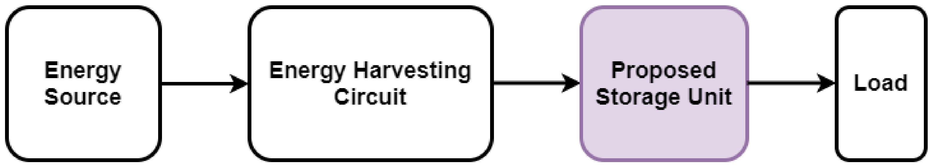
In this work, a novel ultra-low-power integrated storage unit is proposed, suitable for a plethora of energy harvesting autonomous applications (Figure 1). This design is an improved and more versatile version of previous work [18] and presents experimental results. It can be connected to the output of various energy harvesting circuit types (DC-DC converters, charge pumps, etc.) and transfer the harvested energy to the storage media, providing regulated voltage supply to the internal control units of the harvesting circuit and the output loads (e.g., low-power sensors).
The proposed unit achieves minimization of the internal power consumption, deployment area and design complexity. The main storage element is a supercapacitor of small value, while a second larger supercapacitor can be used to provide energy to high-power modules. Depending on the energy availability conditions (continuous or interrupted), a backup battery can be used to avoid the energy starvation of the system during time periods of low input energy. Any type of battery can be used, depending on the use case application. Due to technology restrictions of the proposed unit, its maximum voltage must not exceed 3.6 V. For example, in Section 5.1, two 1.2 V Ni-MH AAA batteries are used to validate the unit’s operation.
The proposed unit provides self-startup operation and sub-μW consumption, highly desired properties that contribute to high energy utilization and power autonomy of the applied harvesting system. Furthermore, it presents enhanced adaptability since it can be integrated into a wide range of energy harvesting systems, considering that the control parameters (supercapacitor thresholds, produced supply voltage) can be modified by the user. Moreover, significant versatility is offered, since external control, e.g., a microcontroller unit, can be added to the topology.
This paper is organized as follows. Section 2 presents the proposed supercapacitor storage unit and its operational principle. Section 3 describes the control logic of the unit. Section 4 and Section 5 show the simulated and experimental results, respectively. Section 6 discusses the utilization of the storage unit in wireless sensor nodes (WSN) applications. Finally, Section 7 concludes this paper.
2. Proposed Topology and Operational Principle
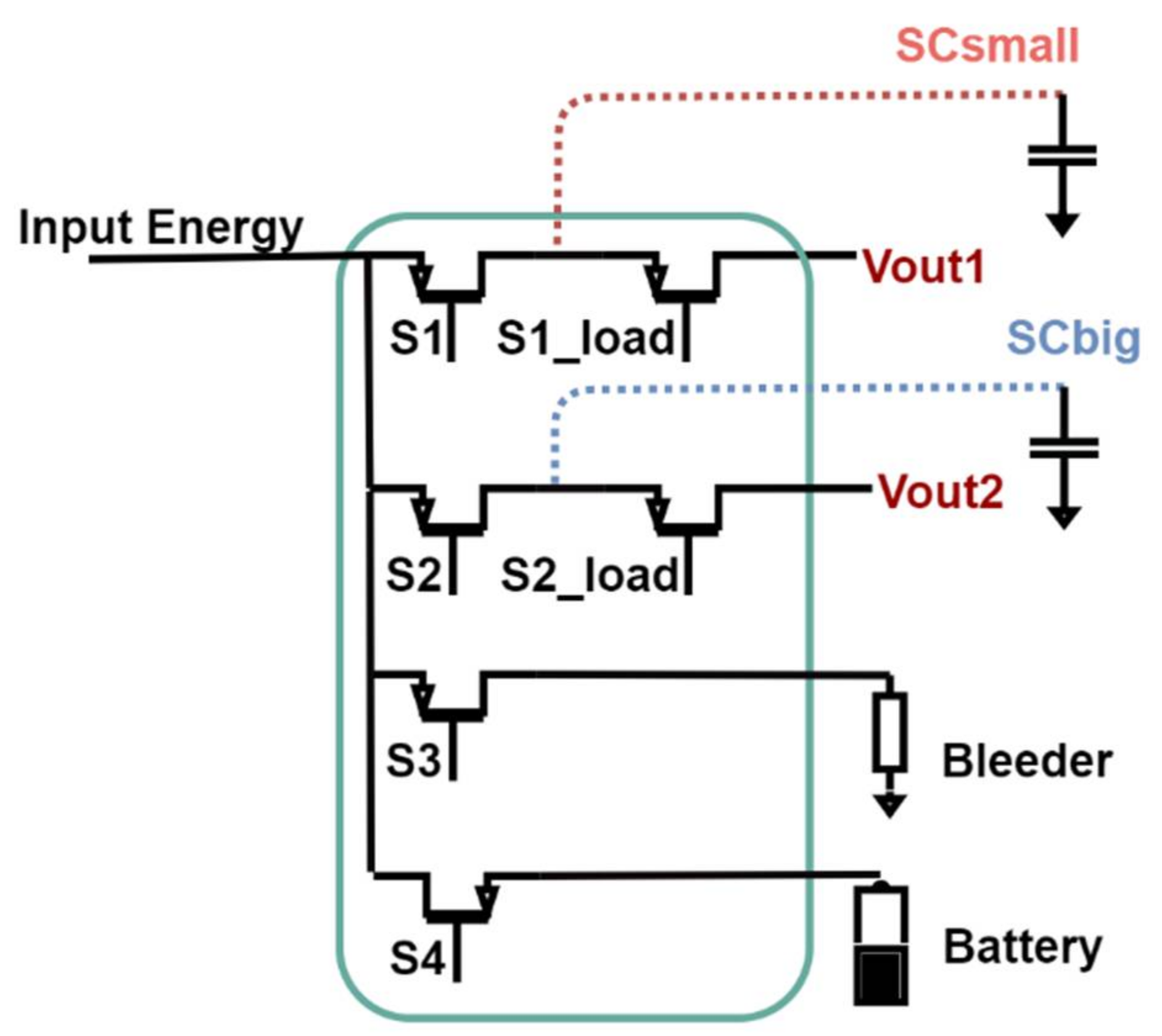
The proposed storage unit is comprised of two supercapacitors, a small (SCsmall), a larger one (SCbig) and a backup battery (Figure 2). The small supercapacitor is mandatory since it is the main storage element that provides power to the control unit. The large supercapacitor and the battery elements are considered optional and their integration on the unit depends on the needs of each specific application.
Specifically, SCsmall provides a regulated supply voltage with a 50 mV voltage ripple for the internal control circuits of the energy harvesting system and power output for connection of external loads (e.g., sensors, processing units, low-range RF modules). The 50 mV voltage ripple is selected to minimize the switching frequency — hence the power consumption — and at the same time, it is considered safe for most load types. SCbig offers an extra unregulated output to the system, for more power demanding loads (e.g., wide-range RF modules, GSM modules), since many off-the-shelf components operate in a wide supply voltage range. The voltage window of this output can be adjusted by the user regarding the specifications of the connected module, with a minimum window of 200 mV. To ensure the extended survival of systems that their continuous operation is critical a backup battery can be connected to the unit. Finally, a bleeder resistor is used to protect the system from excess input energy, which is activated whenever the supercapacitor(s) are fully charged.
The flowchart depicted in Figure 3 summarizes the operational principle of the unit which is described as follows:
Self-Startup: PMOS switches are used to control the charging of the supercapacitors (i.e., switches S1, S2 in Figure 2). Initially, all control signals are at zero potential since the control unit is inactive. Thus, the PMOS switches are ON, and energy is provided to both supercapacitors. As soon as the small supercapacitor voltage (VSCsmall) reaches a sufficient level, the control unit is activated, monitoring the charging of the supercapacitors.
Charging: Initially, the SCsmall supercapacitor starts to charge through switch S1. Meanwhile, SCbig remains disconnected as the main objective is the power-up of the system. The charging process continues until VSCsmall reaches a maximum threshold (Vmax1). At this state, SCbig begins to charge. The charging of SCbig continues until its voltage level reaches a high threshold value (Vmax2), but only if VSCsmall remains within a small voltage window (i.e., ΔV1 = Vmax1 − Vmin1 = 50 mV). This way, SCsmall has always charging priority and supply voltage regulation is achieved for the system internal control unit.
Loads Connection: Two power outputs are available for load connection. A light load can be connected to SCsmall through the switch S1_load. Granted that VSCsmall is above Vmin1, the load supply can be enabled. Power demanding modules can be connected to SCbig. If VSCbig is higher than a lower threshold (Vmin2), the load can be supplied through switch S2_load.
Preservation: In the worst-case scenario, where input energy is not available, a backup battery can provide energy to SCsmall in order to sustain the operation of the system. If needed, the unit can be configured to provide energy to SCbig as well. The battery support is triggered if the supercapacitor’s voltage level drops below the predefined thresholds, Vlow1 and Vlow2, respectively. These thresholds are set lower than Vmin1 and Vmin2, to avoid unnecessary battery activation and the external loads enabling during energy starvation periods. The charging priority feature is also applied here.
Protection: When the supercapacitors are fully charged, a bleeder resistor is connected to the input in order to dump any excess input energy and protect the system from overvoltage stresses.
External control: The charging and discharging thresholds for the supercapacitors are externally selected using resistor dividers. Large value resistor networks should be utilized, for ultra-low power consumption. Alternatively, digital-to-analog converters can be used along with a microcontroller unit (MCU), to dynamically change the thresholds, or even deactivate unnecessary modes by monitoring the available energy and voltage level at the input. Finally, the load outputs can be enabled or disabled by the MCU, through the en1 and en2 pins.
The selection of the supercapacitors values should be based on the needs of each specific application and be decided according to the available input energy and the load’s demands. For instance, if long starvation periods are expected, large supercapacitors should be used, which may increase the required start-up time but will secure the extended survival of the system. Generally, demanding loads that can draw large instant currents during activation (e.g., wide-range RF transmitters) should be connected to SCbig. For SCsmall, a relatively low capacitance is recommended, as it provides fast startup to the system. Finally, for ultra-low-power systems the leakage current of the selected supercapacitors should be considered.
In the proposed design the maximum input current is set to 500 mA and the maximum output current is set to 100 mA. The working voltage thresholds of both supercapacitors can be set anywhere between 1.2 V and 3.6 V.
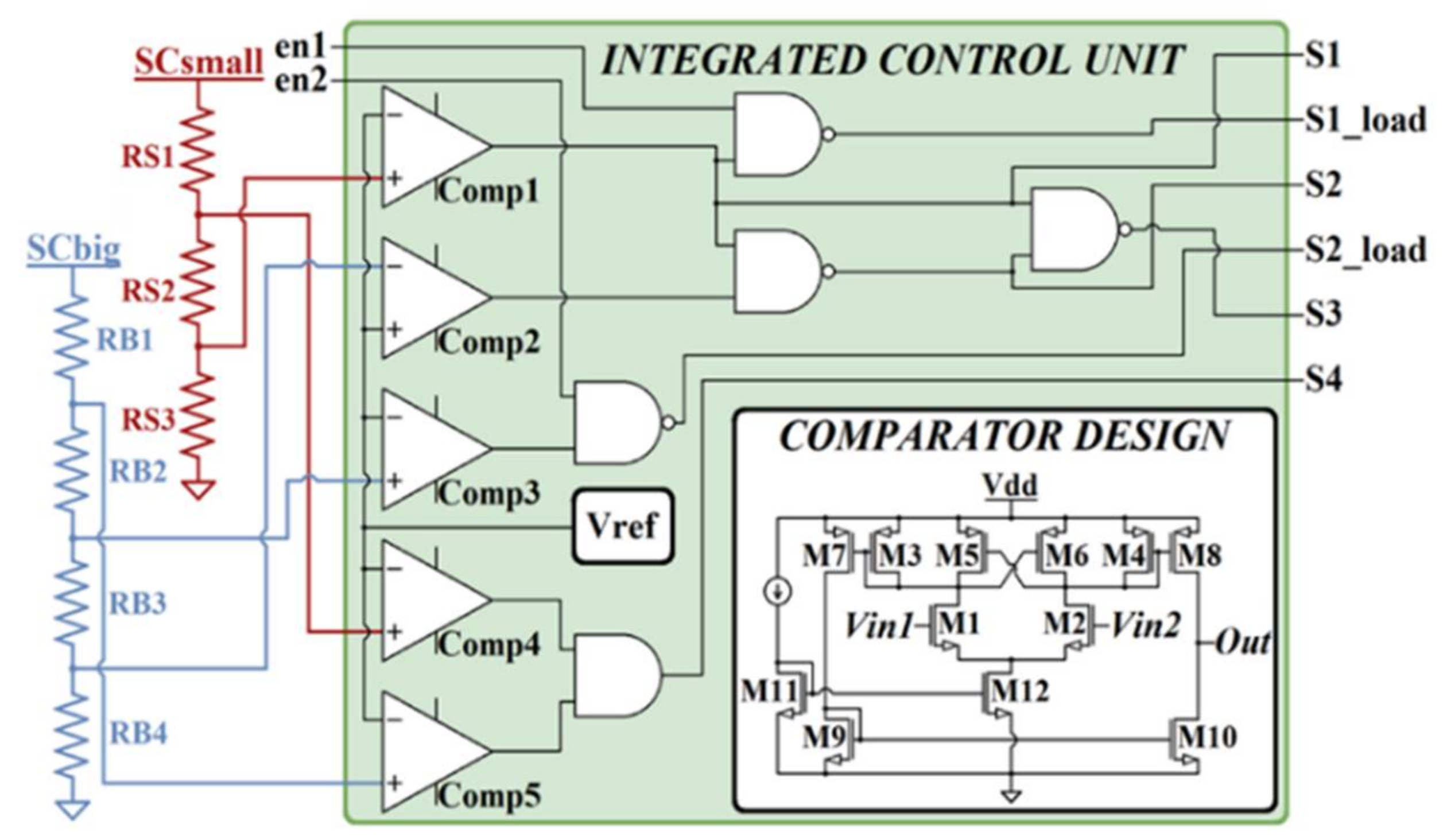
3. Implementation of the Control Unit
The control circuit of the proposed storage unit, composed of comparators, logic gates and power switches, is depicted in Figure 4. The power switches are implemented with 10,000 um/0.30 um 3.3 V PMOS transistors, which present low on-resistance and sufficient response time. The power switch’s length is set to a minimum in order to present a small layout area. A bulk regulation circuit is added on S1 and S2 switches to prevent supercapacitors from discharging towards the input. To supervise the voltage levels of the storage media, low-power comparators are designed, utilizing resistive MOSFETs and nA bias current (Figure 4). The topology of the used comparator [19] creates a hysteresis window (ΔV) which can be implemented by adjusting the cross-coupled (M5, M6) and diode-connected (M3, M4) transistors aspect ratio as follows:
where W is the width of each transistor, L is the length of each transistor and Vovdiffpair is the overdrive voltage of the differential pair of the comparator. Thus, by properly selecting the values of the transistors’ widths, the desired hysteresis window can be achieved. Specifically:
For SCsmall, a comparator with a 50 mV hysteresis window (comp1) is designed. It controls the charging and discharging mode of the supercapacitor through switches S1 and S1_load respectively. This small hysteresis window provides regulated supply voltage for the internal circuits of the harvesting system, with low voltage ripple as well as protection from excessive switching. Additionally, pin en1 is available for external control of the load connection via the S1_load switch (Vout1).
The SCbig charging mode is also supervised by a 50 mV hysteresis window comparator (comp2). Additionally, a 200 mV hysteresis window comparator (comp3) controls the SCbig discharging, via the output switch, S2_load. Since two different comparators are used for the charging and discharging mode of SCbig, the output voltage window (Vout2) can be adjusted to the load needs, with a minimum ΔV2 of 200 mV. For a 5 F capacitor and 100 mA load current the frequency of the voltage ripple is extremely low (<1 mHz). This supply voltage ripple is acceptable for many off-the-shelf components (e.g., MSP430i204x MCU, etc.). As external control is offered (pins en1 and en2), the supply of the loads can be enabled or disabled as needed. Otherwise, the enable pins can be tied to low (inactive) or high (active) potential.
Two additional comparators (comp4 and comp5), monitor VSCsmall and VSCbig voltage levels and activate the battery support if one or both supercapacitors are critically discharged. The S4 switch closes, and the battery provides energy to the supercapacitor in need. The bleeder mode (switch S3) is triggered only in case that both supercapacitors are fully charged.
The combination of the comparators signals along with the external enable signals, is implemented with digital logic circuits (NAND, AND, NOT gates) which are also custom-designed with resistive transistors, to further decrease the power consumption of the control unit.
The voltage thresholds are determined by external voltage divider networks (Figure 4), with multiple voltage tapping points. A fraction of VSCsmall or VSCbig is compared with a stable voltage reference. Since bandgap voltage references are too power-demanding for low-power applications, a 1.08 V voltage reference circuit was implemented, which is based on the circuit presented in [20], with pW power consumption.
4. Simulation Results
In order to verify the operation of the proposed storage unit, simulations were carried out via the Cadence Virtuoso suite. The input voltage of the storage unit was set to 2.4 V, emulating the output voltage of a harvesting circuit, i.e., a step-up DC-DC converter. The charging and discharging voltage thresholds of the supercapacitors were set as follows:
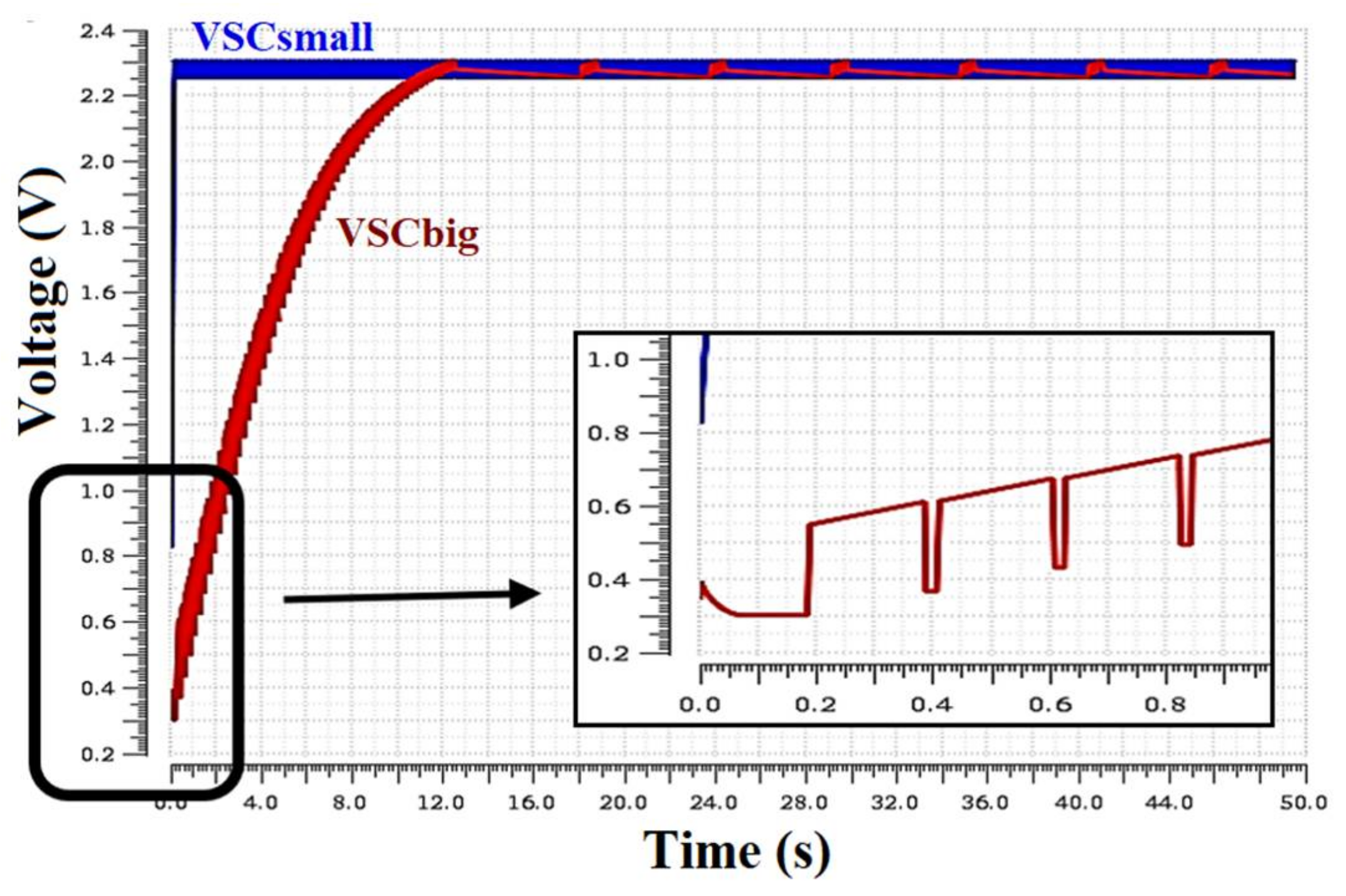
The voltage levels in (2) were implemented with voltage dividers, each with a total resistance of 82 MΩ. An AVX BZ015A104Z_B Bestcap supercapacitor of 100 mF was selected as SCsmall and an SCMT22C505PRBA0 supercapacitor of 5 F as SCbig. To extract realistic results, ESR and leakage resistors were added to the schematic models, according to the supercapacitors datasheets. Figure 5 shows the charging mode when both supercapacitors are fully empty. At startup, a 350 mV early-state charging phase is observed for SCbig, due to the insufficient power supply of the control unit. The duration of this phenomenon depends on the available input power as well as the selected supercapacitors values and their leakage current. For the components under consideration, the charging of SCbig stops after approximately 100 ms.
The supply of the output loads is depicted in Figure 6a,b. A 100 Ω resistor is connected to Vout1 and a 22 Ω resistor to Vout2, drawing approximately 20 mA and 100 mA, respectively. As shown, the loads are connected when the voltage levels of the supercapacitors exceed the minimum thresholds. Figure 7a presents the activation of the bleeder resistor. Figure 7b shows the battery support mode. The battery input voltage is set to 2.5 V, providing energy to the critically discharged supercapacitors, with the defined charging priority. The SCsmall is recharged to the higher desired voltage (i.e., 2.3 V) to provide proper operation to the internal control circuits, while SCbig voltage is maintained to the minimum threshold (i.e., 1.6 V) to avoid unnecessary usage of the backup battery.
The simulated total current consumption of the storage unit is 374 nA at 2.3 V. The voltage dividers of the comparators consume 56 nA (28 nA each) and the integrated control circuit draws 318 nA.
5. Experimental Results
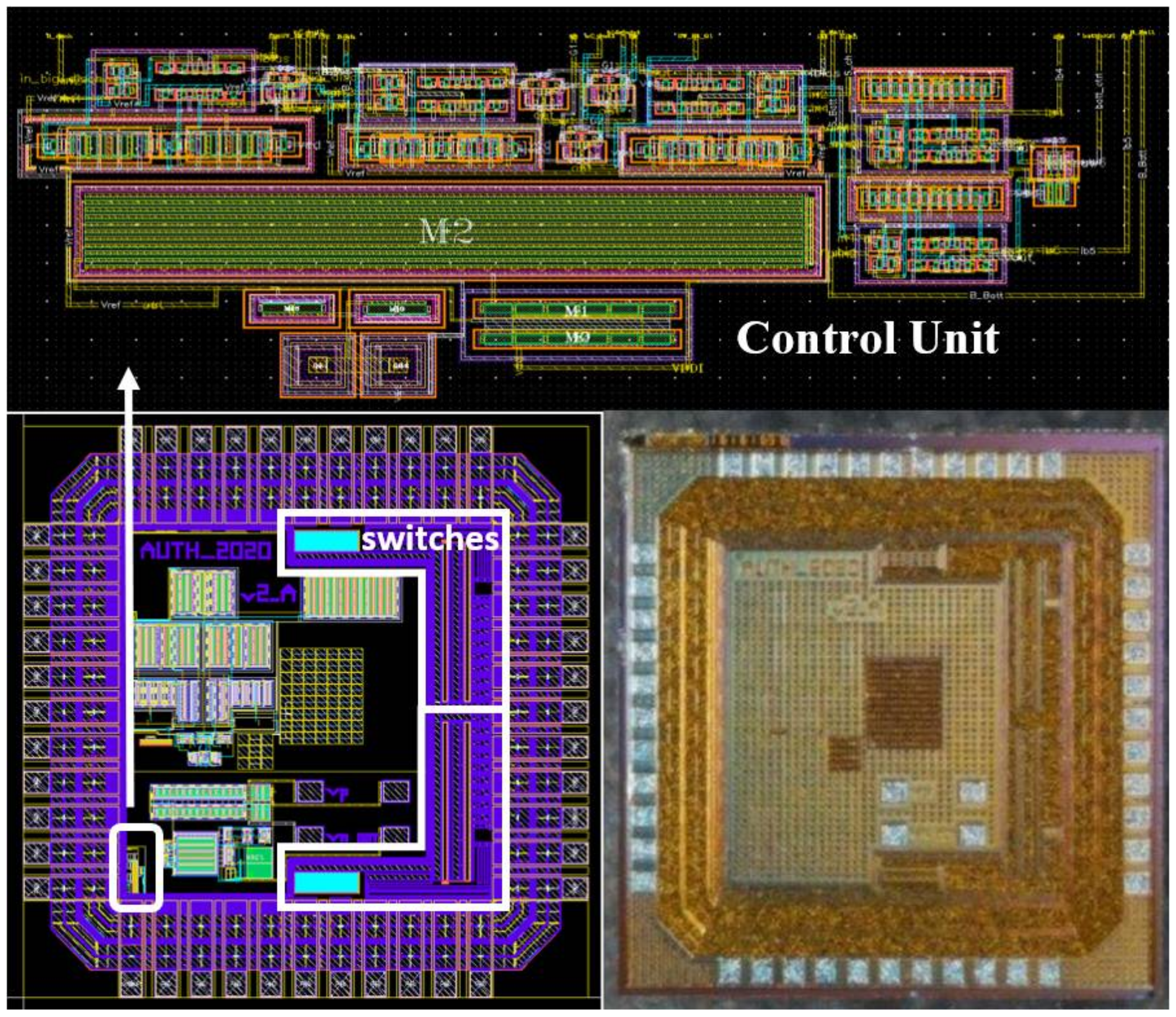
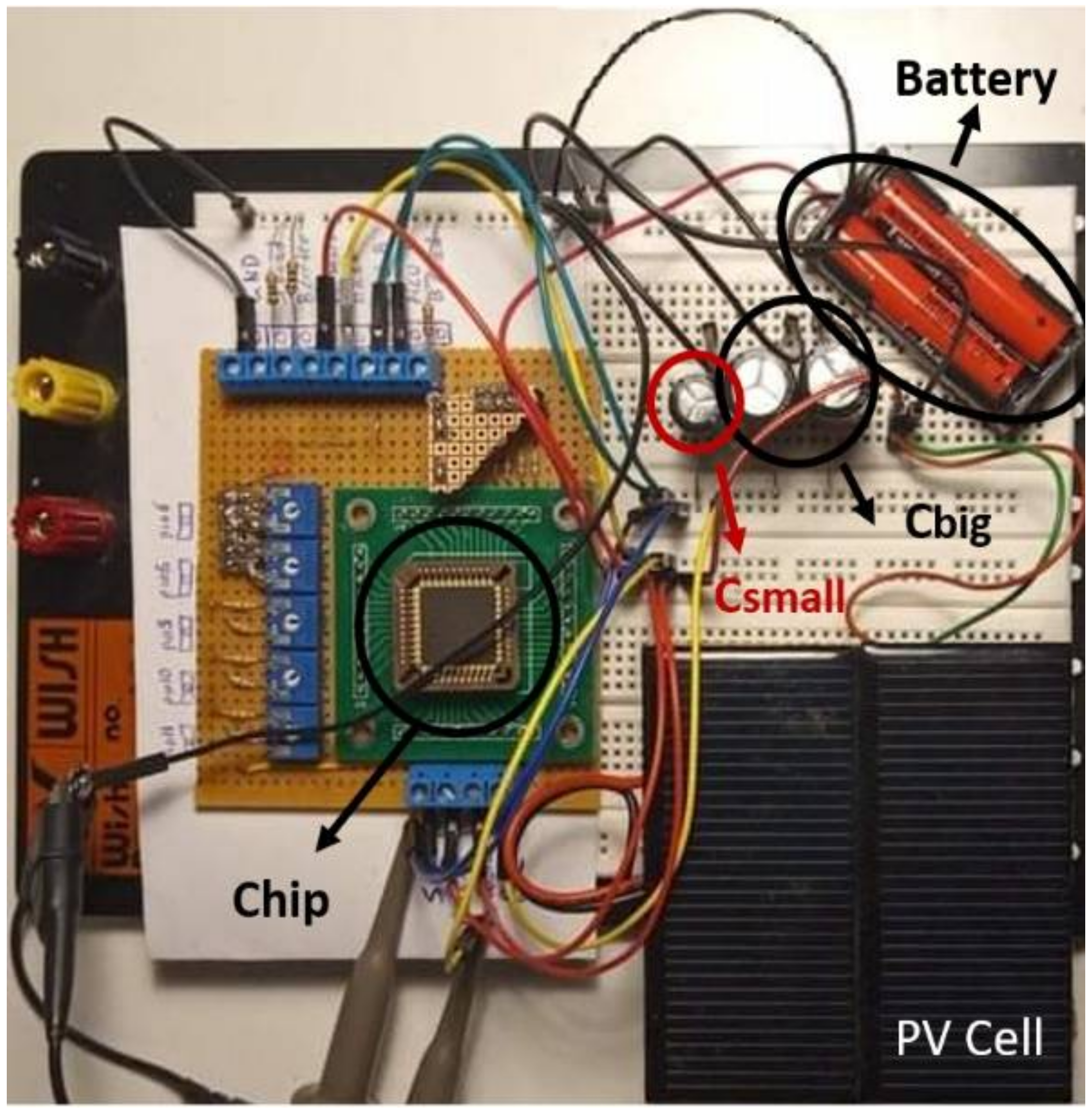
The proposed self-adaptive storage scheme was implemented in a 0.18 um standard CMOS process. The physical design and the chip die are shown in Figure 8. The control unit layout occupies a low die area of 125 um × 50 um.
5.1. Laboratory Measurements
To test the fabricated design, laboratory measurements were carried out using a digital oscilloscope (RIGOL DS1052E), as depicted in Figure 9, Figure 10 and Figure 11. Voltage dividers with a total resistance of 82 MΩ were utilized for the thresholds of the comparators, according to Equation (2). Additionally, the AVX supercapacitors mentioned in Section 4 were used. A voltage source unit provides 2.4 V to the storage scheme input.
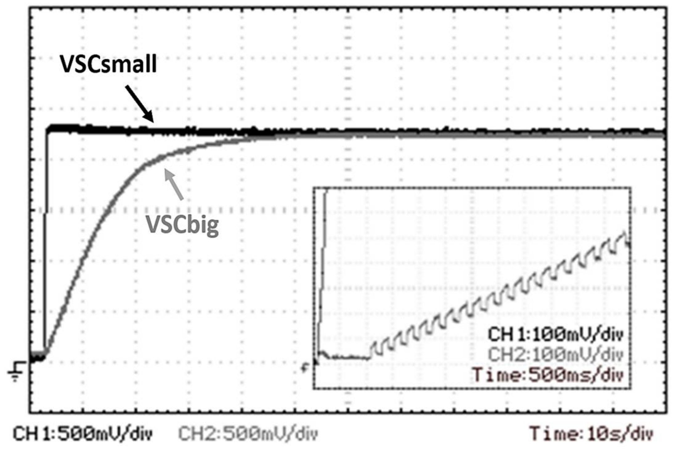
Figure 9 demonstrates the supercapacitors charging mode. Initially, SCsmall begins to charge and only when it is fully charged at the voltage of 2.3 V determined from the thresholds of the comparators, SCbig is connected at the input. As shown, the early-state charging of SCbig stops at about 50 mV, lower than the simulation result, and the overall charging duration is longer. These phenomena are due to the charging path resistance (i.e., chip pins and breadboard PCB resistance), which reduces the charging current. The peak current drawn is 2.1 A in the simulation, while its experimentally measured value is 0.45 A.
The load’s connection modes are depicted in Figure 10a,b. A 100 Ω resistor is connected to Vout1 and a 22 Ω resistor to Vout2, similarly to the simulation setup. The loads draw energy from the supercapacitors, as long as the voltage levels do not fall below the predetermined minimum thresholds. Figure 11a presents the bleeder activation, drawing the excess energy. Figure 11b curves are obtained without input power supply. The supercapacitors are discharged, and two 1.2 V Ni-MH AAA batteries, connected in series (measured at 2.5 V), provide power to the system.
The measured current consumption of the integrated control unit is 376 nA at 2.3 V. Combined with the two 82 MΩ voltage dividers consumption, the total current consumption of the proposed unit is 432 nA at 2.3 V.
In Table 1, this work is compared with other state-of-the-art implementations. As shown, the proposed design offers many advantages such as low-complexity, small size integrated solution, ultra-low-power consumption and wide voltage and current range. Thus, this design is suitable for a wide variety of autonomous energy harvesting applications.
5.2. Energy Harvesting
The storage unit was also tested during the energy harvesting operation. A BQ25504 energy harvesting IC combined with an 80 mm × 72 mm PV cell were utilized, harnessing energy at office lighting conditions (approximately 600 Lux of light intensity). The measurement setup is depicted in Figure 12. As this is a low power demanding use case scenario, the values of SCsmall and SCbig were set at 1 mF and 4.4 mF (two 2.2 mF capacitors connected in parallel) respectively.
Figure 13 presents the charging phase of the storage unit, with zero initial stored energy in the two supercapacitors. Since the available current is about 100 uA, the charging of the small supercapacitor requires about 30 s.
As stated, the supercapacitor’s values should be properly selected, according to the power supply requirements of the target system. For this test case, smaller capacitors can reduce the charging time duration, at the expense of extended energy autonomy or connection of demanding external loads.
The proposed unit was also tested with a piezoelectric transducer providing power at the input. Figure 14 depicts the measurement setup. A V25W PZT transducer from MIDE is used to convert the vibrations to electrical energy and a vibrating speaker is used to trigger the piezoelectric transducer. A mass of 1.9 g. is fixed on the tip of the transducer, to further increase the power offered to the storage unit. A rectifier comprised of four Schottky diodes is connected between the output of the PZT element and the proposed storage unit. The vibrations frequency is set at 25 Hz and the open circuit peak-to-peak voltage is measured at 20 V. The observed mechanical displacement of the tip of the transducer was observed at 1 cm peak-to-peak. The values of SCsmall and SCbig were set at 1 mF and 4.4 mF respectively, and also, loads of 100 Ω are connected at the supercapacitors outputs. Finally, Figure 15 presents the charging phase of the two supercapacitors.
6. Future Work and Discussion
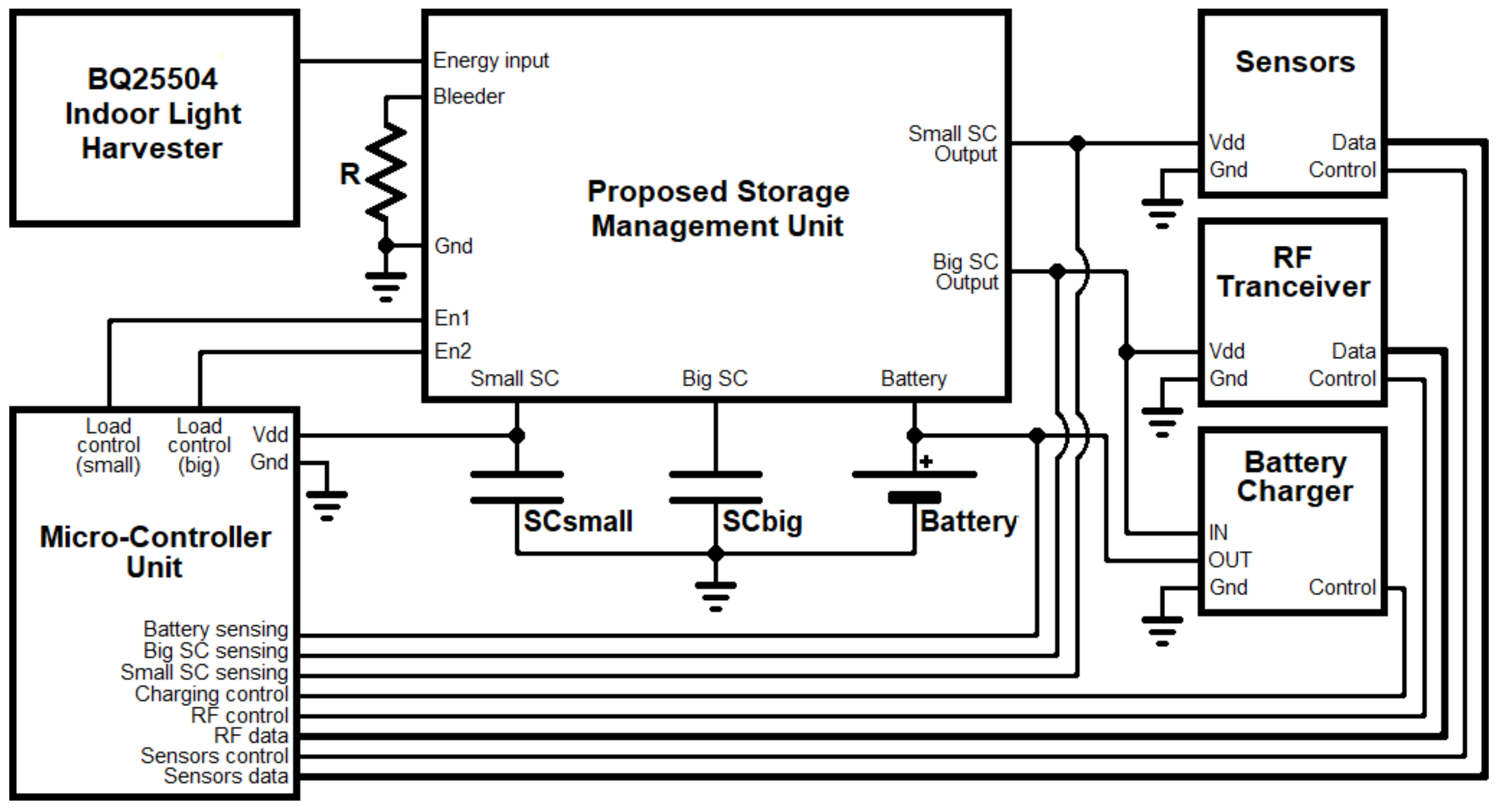
The proposed storage unit is suitable for energy-harvesting-based, wireless sensor node (WSN) applications. The unit can autonomously supervise the charging and discharging of two supercapacitors (SCsmall, SCbig) and a backup battery, exploiting the energy provided by a harvester module. It can be combined with any type of energy harvesting module, such as photovoltaic, triboelectric, piezoelectric, or thermoelectric micro/nano-generators. Depending on the used harvester, a step-up/down converter and/or an AC-DC rectifier might be required (e.g., BQ25504 in case of the small photovoltaic panel or thermoelectric harvester). The proposed storage unit provides two separate power outputs. The SCsmall output, which provides a regulated output voltage (50 mV ripple) has the highest charging priority. Thus, it is considered as the main power output of the unit and should be used for the primary system circuits. Additionally, the SCbig output, provides an unregulated output voltage, however within an adjustable voltage window, with a minimum ΔV of 200 mV. This output has low charging priority and should be used for the secondary circuits of the system. This way extended operation is achieved for the primary system circuits, and additionally, the idle consumption of the secondary ones is eliminated. For embedding an RF transceiver module, an MCU, as well as the required sensors, and in case that real-time acquiring of the sensor data is not mandatory, the SCsmall output can be used for the MCU supply and the sensors supply (for local data logging) and the SCbig output can be used for the power demanding RF transceiver module (so the transmission of the data will take place during energy-rich periods of time).
In the case of continuous energy availability (e.g., continuous vibrations), a battery is not required and can be omitted. However, to ensure undisrupted operation a backup non-rechargeable battery can be added. For ultra-low-power WSN systems and sparse energy starvation periods, a multiyear duration is expected from a coin-size battery cell (e.g., cr2032 3V 230 mah). In case of discontinuous energy availability conditions and for a scenario that the undisrupted operation of the supported system is crucial, the use of a battery is mandatory. Depending on the use-case application and the power requirements, the use of a separate external battery charger module should also be considered. Finally, in systems embedding an MCU, the direct power supply of the MCU from the SCsmall is possible. This way the MCU supply has the highest priority and the longest possible power autonomy. A future work WSN approach is shown in Figure 16.
In the WSN shown in Figure 16, an indoor light harvester based on the BQ25504 IC was used. Additionally, an ultra-low-power MCU (e.g., MSP430FR5969 consuming 20 nA in deep sleep mode and 250 nA with calendar and timekeeping ON) is directly supplied by the small supercapacitor. Since continuous energy availability is not expected and an MCU is used, a rechargeable battery and a battery charger are added to the topology. The MCU is measuring the voltage levels of the two supercapacitors and the battery, in order to select a preferable power plan that matches the available energy. For example, only calendar and timekeeping during very-low energy levels, sensor reading during low energy levels, data transmission during high energy levels and battery charging during very-high-energy levels. The MCU is also controlling all the peripheral modules (sensors, RF transceiver and battery charger), as well as the load control signals (en1, en2) of the proposed storage unit.
7. Conclusions
In this work, an ultra-low-power supercapacitor-based storage unit with an integrated control scheme was presented, offering flexibility to the applied energy harvesting system. The ultra-low current consumption of only 432 nA at 2.3 V proves the proposed storage unit ideal for energy harvesting systems, even for cases of a few μW input power range. Furthermore, extra modes can be added to the topology with the usage of external control (e.g., an MCU), expanding the operational capabilities of the proposed unit. For instance, the control of an additional charging unit for the backup battery is a highly beneficial mode that will be added in future work.
Author Contributions
Conceptualization, V.G.; methodology, E.K., G.D.; validation, V.G., K.K.; writing—original draft preparation, V.G., S.S.; writing—review and editing, V.G., E.K., S.S.; supervision, S.S. All authors have read and agreed to the published version of the manuscript.
Funding
This research was co-financed by the European Regional Development Fund of the European Union and Greek national funds through the Operational Program Competitiveness, Entrepreneurship and Innovation, under the call RESEARCH—CREATE—INNOVATE (project code: T1EDK-00360).
Conflicts of Interest
The authors declare no conflict of interest.
References
- Elahi, H.; Munir, K.; Eugeni, M.; Atek, S.; Gaudenzi, P. Energy Harvesting towards Self-Powered IoT Devices. Energies 2020, 13, 5528. [Google Scholar] [CrossRef]
- Chen, I.-C.; Liang, C.-W.; Tsai, T.-H. A single-inductor dual-input dual-output DC–DC converter for photovoltaic and piezoelectric energy harvesting systems. IEEE Trans. Circuits Syst. II Express Briefs 2019, 66, 1763–1767. [Google Scholar] [CrossRef]
- Charris, D.; Gomez, D.; Ortega, A.R.; Carmona, M.; Pardo, M. A Thermoelectric Energy Harvesting Scheme with Passive Cooling for Outdoor IoT Sensors. Energies 2020, 13, 2782. [Google Scholar] [CrossRef]
- Sanislav, T.; Mois, G.D.; Zeadally, S.; Folea, S.C. Energy Harvesting Techniques for Internet of Things (IoT). IEEE Access 2021, 9, 39530–39549. [Google Scholar] [CrossRef]
- Salauddin, M.; Halim, M.A.; Park, J.Y. A magnetic-spring-based, low-frequency vibration energy harvester comprising a dual halbach array. Smart Mater. Struct. 2016, 25, 095017. [Google Scholar] [CrossRef]
- Toyabur, R.M.; Salauddin, M.; Park, J.Y. Design and experiment of piezoelectric multimodal energy harvester for low frequency vibration. Ceram. Int. 2017, 43, 675–681. [Google Scholar] [CrossRef]
- Salauddin, M.; Toyabur, R.M.; Maharjan, P.; Rasel, M.S.; Cho, H.; Park, J.Y. Design and experimental analysis of a low-frequency resonant hybridized nanogenerator with a wide bandwidth and high output power density. Nano Energy 2019, 66, 104122. [Google Scholar] [CrossRef]
- Prauzek, Μ.; Konecny, J.; Borova, M.; Janosova, K.; Hlavica, J.; Musilek, P. Energy harvesting sources storage devices and system topologies for environmental wireless sensor networks: A review. Sensors 2018, 18, 2446. [Google Scholar] [CrossRef] [PubMed] [Green Version]
- Babu, T.S.; Vasudevan, K.R.; Ramachandaramurthy, V.K.; Sani, S.B.; Chemud, S.; Lajim, R.M. A comprehensive review of hybrid energy storage systems: Converter topologies control strategies and future prospects. IEEE Access 2020, 8, 148702–148721. [Google Scholar] [CrossRef]
- Khan, M.A.; Zeb, K.; Sathishkumar, P.; Ali, M.U.; Uddin, W.; Hussain, S.; Ishfaq, M.; Khan, I.; Cho, H.-G.; Kim, H.-J. A Novel Supercapacitor/Lithium-Ion Hybrid Energy System with a Fuzzy Logic-Controlled Fast Charging and Intelligent Energy Management System. Electronics 2018, 7, 63. [Google Scholar] [CrossRef] [Green Version]
- Ravada, B.R.; Tummuru, N.R.; Ande, B.N.L. Photovoltaic-Wind and Hybrid Energy Storage Integrated Multi-Source Converter Configuration for DC Microgrid Applications. IEEE Trans. Sustain. Energy 2021, 12, 83–91. [Google Scholar] [CrossRef]
- Hussain, S.; Ali, M.U.; Park, G.-S.; Nengroo, S.H.; Khan, M.A.; Kim, H.-J. A Real-Time Bi-Adaptive Controller-Based Energy Management System for Battery–Supercapacitor Hybrid Electric Vehicles. Energies 2019, 12, 4662. [Google Scholar] [CrossRef] [Green Version]
- Pellitteri, F.; Livreri, P.; Schirone, L.; Miceli, R. A hybrid storage system for wireless sensor nodes powered with energy harvesting. In Proceedings of the 2019 International Conference on Clean Electrical Power (ICCEP), Otronto, Italy, 2–4 July 2019; pp. 221–226. [Google Scholar]
- Saggini, S.; Ongaro, F.; Galperti, G.; Mattavelli, P. Supercapacitor-based hybrid storage systems for energy harvesting in wireless sensor networks. In Proceedings of the 2010 Twenty-Fifth Annual IEEE Applied Power Electronics Conference and Exposition (APEC), Palm Springs, CA, USA, 21–25 February 2010; pp. 2281–2287. [Google Scholar]
- Qi, N.; Yin, Y. Comprehensive optimized hybrid energy storage system for long-life solar-powered wireless sensor network nodes. Appl. Energy 2021, 290, 116780. [Google Scholar] [CrossRef]
- Siskos, A.; Mahboubi, F.E.; Boitier, V.; Laopoulos, T.; Bafleur, M. A power management system using reconfigurable storage scheme for batteryless wireless sensor nodes. In Proceedings of the 2018 7th International Conference on Modern Circuits and Systems Technologies (MOCAST), Thessaloniki, Greece, 7–9 May 2018; pp. 1–4. [Google Scholar]
- Li, J.; Seo, J.-S.; Kymissis, I.; Seok, M. Triple-mode hybrid-storage energy harvesting power management unit: Achieving high efficiency against harvesting and load power variabilities. IEEE J. Solid-State Circuits 2017, 52, 2550–2562. [Google Scholar] [CrossRef]
- Gogolou, V.; Siskos, S.; Laopoulos, T. A reconfigurable storage unit for autonomously powered IoT nodes. In Proceedings of the 2019 Panhellenic Conference on Electronics & Telecommunications (PACET), Volos, Greece, 8–9 November 2019; pp. 1–4. [Google Scholar]
- Amin, S.S.; Mercier, P.P. MISIMO: A multi-input single-inductor multi-output energy harvesting platform in 28-nm FDSOI for powering net-zero-energy systems. IEEE J. Solid-State Circuits 2018, 53, 3407–3419. [Google Scholar] [CrossRef]
- Ji, Y.; Lee, J.; Kim, B.; Park, H.-J.; Sim, J.-Y. A 192-pW voltage reference generating bandgap–Vth with process and temperature dependence compensation. IEEE J. Solid-State Circuits 2019, 54, 3281–3291. [Google Scholar] [CrossRef]
Figure 1.
Block diagram of an energy harvesting system.

Figure 2.
The topology of the proposed energy storage unit.

Figure 3.
A flowchart of the proposed system operational logic.

Figure 4.
Control logic and comparator design.

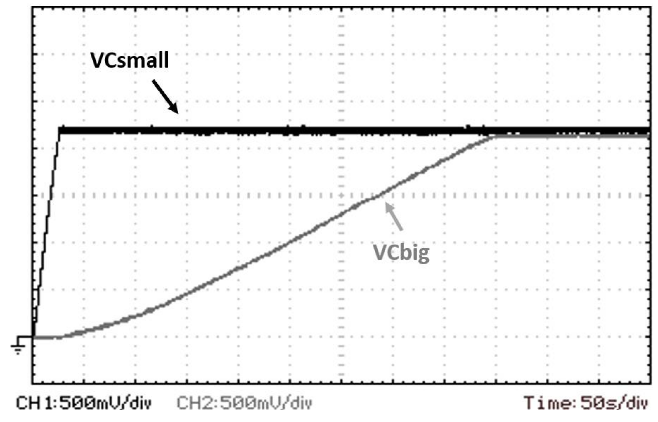
Figure 5.
Supercapacitors charging mode and startup (inset).

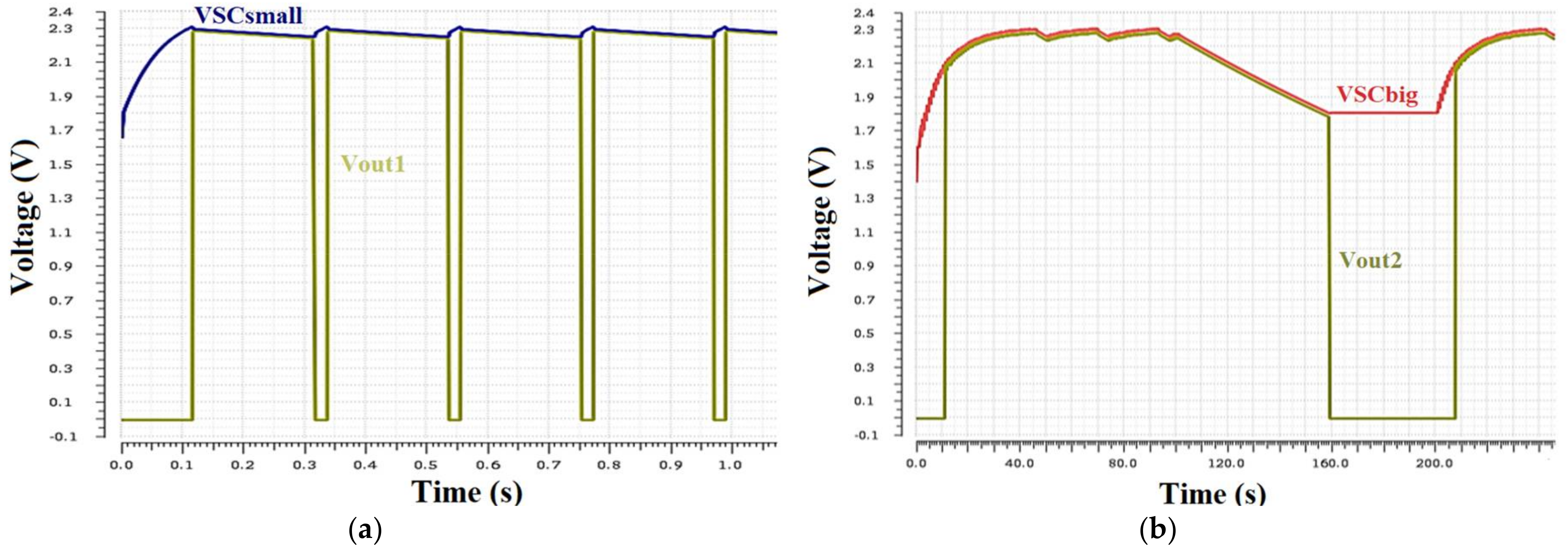
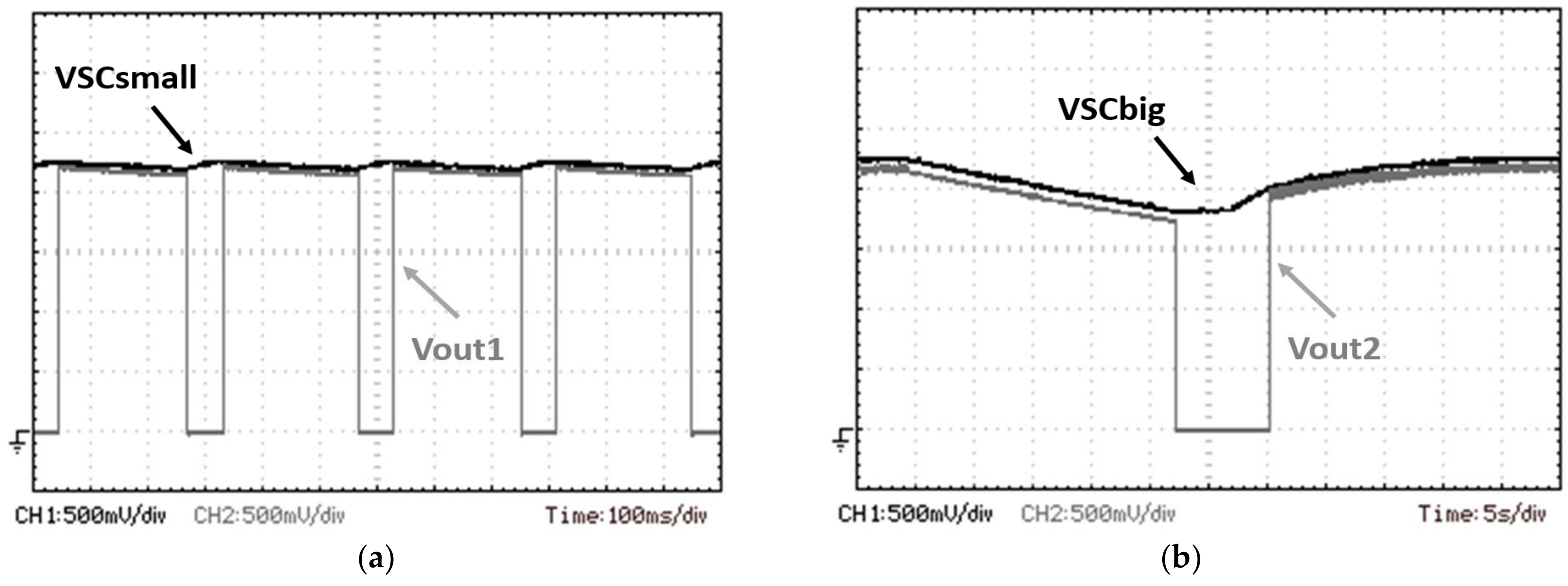
Figure 6.
Connection of the external loads according to the predefined voltage thresholds of the supercapacitors. The output loads are disconnected in low-input energy conditions to preserve the operation of the system. (a) SCsmall voltage level and Vout1 load output. (b) SCbig voltage and Vout2 load output.

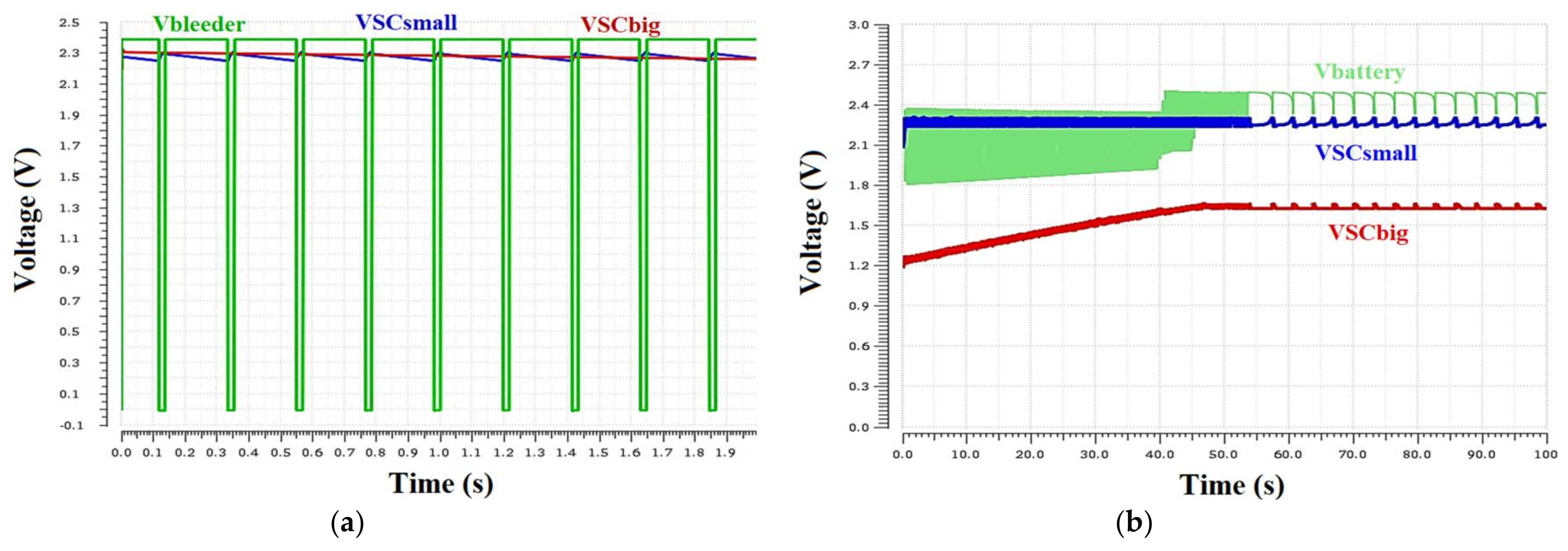
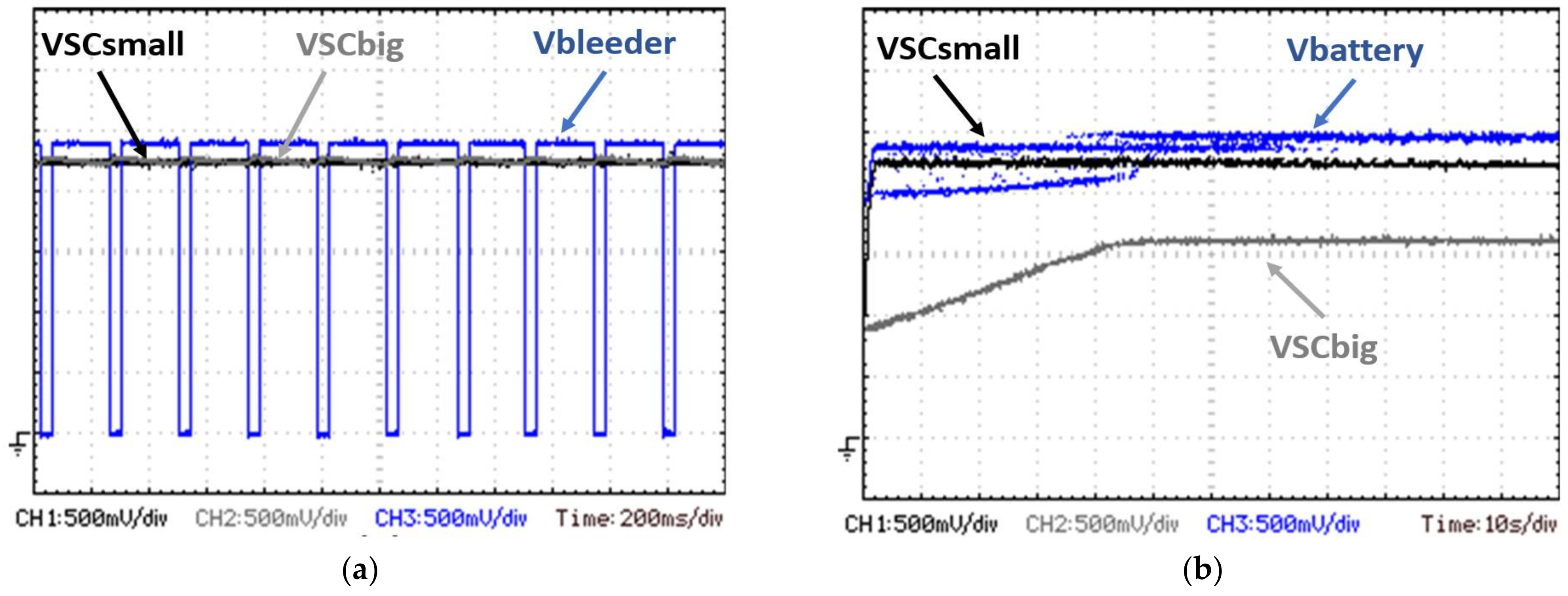
Figure 7.
(a) Bleeder mode activation. The bleeder mode is activated only when both supercapacitors are fully charged. (b) Battery energy support. Initially, the battery charges both supercapacitors. SCbig charging stops when its voltage reaches the lower voltage threshold (1.6 V). SCsmall is charged to its high threshold (2.3 V).

Figure 8.
Physical design of the unit and the fabricated die.

Figure 9.
Oscilloscope view of SCsmall (CH1) and SCbig (CH2) voltage signals during charging and startup (inset), following the predefined charging priority feature. The SCbig supercapacitor is connected to the input only when SCsmall is fully charged at 2.3 V.
Figure 9.
Oscilloscope view of SCsmall (CH1) and SCbig (CH2) voltage signals during charging and startup (inset), following the predefined charging priority feature. The SCbig supercapacitor is connected to the input only when SCsmall is fully charged at 2.3 V.

Figure 10.
Oscilloscope view of (a) SCsmall voltage (CH1) and Vout1 (CH2) load output. (b) SCbig voltage (CH1) and Vout2 (CH2) load output. The output loads are disconnected in low-input energy conditions to preserve the operation of the system.
Figure 10.
Oscilloscope view of (a) SCsmall voltage (CH1) and Vout1 (CH2) load output. (b) SCbig voltage (CH1) and Vout2 (CH2) load output. The output loads are disconnected in low-input energy conditions to preserve the operation of the system.

Figure 11.
(a) SCsmall voltage (CH1), SCbig voltage (CH2) and bleeder output (CH3) during bleeder mode activation. (b) SCsmall voltage (CH1), SCbig voltage (CH2) and battery input (CH3) during battery energy support.
Figure 11.
(a) SCsmall voltage (CH1), SCbig voltage (CH2) and bleeder output (CH3) during bleeder mode activation. (b) SCsmall voltage (CH1), SCbig voltage (CH2) and battery input (CH3) during battery energy support.

Figure 12.
Experimental setup for testing the storage unit in indoor light energy harvesting conditions.
Figure 12.
Experimental setup for testing the storage unit in indoor light energy harvesting conditions.

Figure 13.
SCsmall (CH1) and SCbig (CH2) charging via BQ25504.

Figure 14.
Experimental setup for testing the storage unit with mechanical vibrations harvesting.

Figure 15.
SCsmall (CH1) and SCbig (CH2) charging phase from the piezoelectric transducer.

Figure 16.
Future work WSN topology.


Table 1.
State-of-the-art storage units implementations.
| Ref No. | Target Application | Topology | Technology/Area | Voltage Converters/Inductors/Supercapacitors/Battery | Voltage Range/Maximum Current | Power Consumption |
|---|---|---|---|---|---|---|
| [10] | Electric powered wheelchair | Battery, voltage converter, supercapacitor | Discrete | 2/3/Array/Yes | 60 V/100 A | mW 1 |
| [11] | DC Microgrid | Battery, voltage converter, supercapacitor | Discrete | 1/2/Array/Yes | 50 V/3 A | n/a |
| [13] | Energy harvesting, wireless sensor node | Supercapacitor, bidirectional converter, battery | Discrete | 1/1/1/Yes | 7–12 V/1.25 A | mW 1 |
| [14] | Energy harvesting, wireless sensor node | Supercapacitor, bidirectional converter, battery | Discrete | 1/1/1/Yes | 3.3 V/1.51 A | mW 1 |
| [15] | Energy harvesting, wireless sensor node | Battery, voltage converter, supercapacitor | Discrete | 1/2/1/Yes | 3.3 V/151 mA | uW 1 |
| [16] | Energy harvesting, wireless sensor node | Four supercapacitor reconfigurable power bank | 0.35 um/n/a | 0/0/4/No | 2.6–5.5 V/50 mA | 185 uW |
| [17] | Energy harvesting, wireless sensor node | Supercapacitor (main), battery and converter (secondary) | 65 nm/0.48 mm2 | 2/0/1/Yes | 0.45 V/300 mA | uW 1 |
| This work | Energy harvesting, wireless sensor node | Up to two supercapacitors, optional battery | 0.18 um/0.19 mm2 | 0/0/2/Optional | 1.2V–3.6 V/100 mA | 0.99 uW |
1 Actual value not available.
Publisher’s Note: MDPI stays neutral with regard to jurisdictional claims in published maps and institutional affiliations. |
© 2021 by the authors. Licensee MDPI, Basel, Switzerland. This article is an open access article distributed under the terms and conditions of the Creative Commons Attribution (CC BY) license (https://creativecommons.org/licenses/by/4.0/).
Share and Cite
MDPI and ACS Style
Gogolou, V.; Kozalakis, K.; Koutroulis, E.; Doumenis, G.; Siskos, S. An Ultra-Low-Power CMOS Supercapacitor Storage Unit for Energy Harvesting Applications. Electronics 2021, 10, 2097. https://doi.org/10.3390/electronics10172097
AMA Style
Gogolou V, Kozalakis K, Koutroulis E, Doumenis G, Siskos S. An Ultra-Low-Power CMOS Supercapacitor Storage Unit for Energy Harvesting Applications. Electronics. 2021; 10(17):2097. https://doi.org/10.3390/electronics10172097
Chicago/Turabian StyleGogolou, Vasiliki, Konstantinos Kozalakis, Eftichios Koutroulis, Gregory Doumenis, and Stylianos Siskos. 2021. "An Ultra-Low-Power CMOS Supercapacitor Storage Unit for Energy Harvesting Applications" Electronics 10, no. 17: 2097. https://doi.org/10.3390/electronics10172097
Note that from the first issue of 2016, this journal uses article numbers instead of page numbers. See further details here.