Design of an Highly Efficient AC-DC-AC Three-Phase Converter Using SiC for UPS Applications


1
Graduate Program in Electrical Engineering, Universidade Federal de Minas Gerais, Av. Antônio Carlos 6627, Belo Horizonte—MG 31270-901, Brazil
2
Department of Electronic Engineering, Universidade Federal de Minas Gerais, Av. Antônio Carlos 6627, Belo Horizonte—MG 31270-901, Brazil
*
Author to whom correspondence should be addressed.
†
These authors contributed equally to this work.
Electronics 2018, 7(12), 425; https://doi.org/10.3390/electronics7120425
Submission received: 6 November 2018
/
Revised: 5 December 2018
/
Accepted: 6 December 2018
/
Published: 11 December 2018
(This article belongs to the Section Power Electronics)
Abstract
:With the constant increase of energy consumption in the world, the efficiency of systems and equipment is becoming more important. Uninterruptible Power Supply (UPS) is an equipment that provides safe and reliable supply for critical load systems, that is, systems where a supply interruption can lead to economical or even human losses. The Double Conversion UPS is the most complete UPS class in terms of load protection, regulation, performance, and reliability, however, it has lower efficiency and higher cost because of its high number of power converters. Silicon Carbide devices are emerging as an opportunity to construct power converters with higher efficiency and higher power density. The main purpose of this work is to design a three-phase AC-DC-AC converter using Silicon Carbide for Double Conversion UPS applications. The aim is to maximize efficiency and minimize volume and mass. The methodologies to size and choose the main hardware components are described in detail. Experimental results obtained with the prototype prove the high efficiency and high power density achievable with Silicon Carbide Metal Oxide Semiconductor Field Effect Transistor (MOSFETs).
1. Introduction
Currently, final energy consumption in the form of electricity accounts for a large share of the world’s energy consumption, and may reach more than 50% in some countries [1]. In developing countries, the consumption of electric energy presents accelerated growth, for example, it has increased about 56% in Brazil and 455% in China between 2000 and 2014 [1]. Against this scenario, rational use of electricity and energy efficiency of the generation-storage-distribution-consumption cycle become very important for engineers and researchers that aim the sustainable development.
Among the various types of loads present in the electrical system, we can highlight the critical loads, that is, loads that cannot have the supply of electricity interrupted regardless of the environmental conditions and failures in the electrical system. Examples of critical loads are: Telecommunications and information technology systems, hospital equipment, and banking systems. In order to supply such loads, Uninterruptible Power Supplies (UPS) are often used.
According to the topology or configuration, UPS can be classified as double conversion, passive standby, and line interactive types [2,3]. Double conversion UPS is generally preferred because of the wide tolerance to input voltage variation, output voltage regulation and high system reliability [2,3]. A conventional three-phase double conversion UPS usually contains a rectifier, battery charger, battery pack, inverter, and by-pass switches.
Three-phase UPSs found commercially and in scientific work are based, with slight variations, on a classical topology employing two-level PWM converters [4,5,6,7]. Despite being able to maintain power quality on both the mains side and the load side, its efficiency is limited due to the large switching losses in the electronic switches.
For the sake of improving UPS system’s performance, the use of three-level topologies in the rectifier and in the inverter [8,9] has been proposed. The proposed converters can achieve high efficiency, however the complexity and number of electronic switches increases considerably. In order to find a compromise between performance, cost and complexity, hybrid converters can be used, combining different topologies on the inverter side and on the rectifier side [10].
Despite being a mature technology, silicon power transistors have limitations in terms of switching performance due to reverse recovery from diodes and IGBT tail current which significantly increase switching losses [11]. One approach to overcome these limitations and to improve the performance of electronic converters is the use of transistors made of materials with wide bandgap (WBG), such as Silicon Carbide (SiC) and Gallium Nitride (GaN). Several studies have demonstrated the possibility of applying SiC and GaN transistors in converters operating at high switching frequencies, high voltages, and high working temperature [11,12,13,14], including in the UPS sector for single-phase converters [15,16]. The characteristics of such materials allow the construction of equipment with smaller passive elements, smaller heat sinks, and at the same time improve the efficiency of the system [17].
In the cited circumstances, this work intents to design a more compact three-phase AC-DC-AC converter for UPS applications using silicon carbide and advanced topologies. The resulting converter should have higher efficiency and higher power density in relation to commercially available equipment, thus becoming more competitive in the market. The focus of this work is the AC-DC-AC conversion chain, so the investigation of auxiliary circuits such as by-pass switches, battery charger, and DC-link balance leg will not be made.
2. UPS Specifications
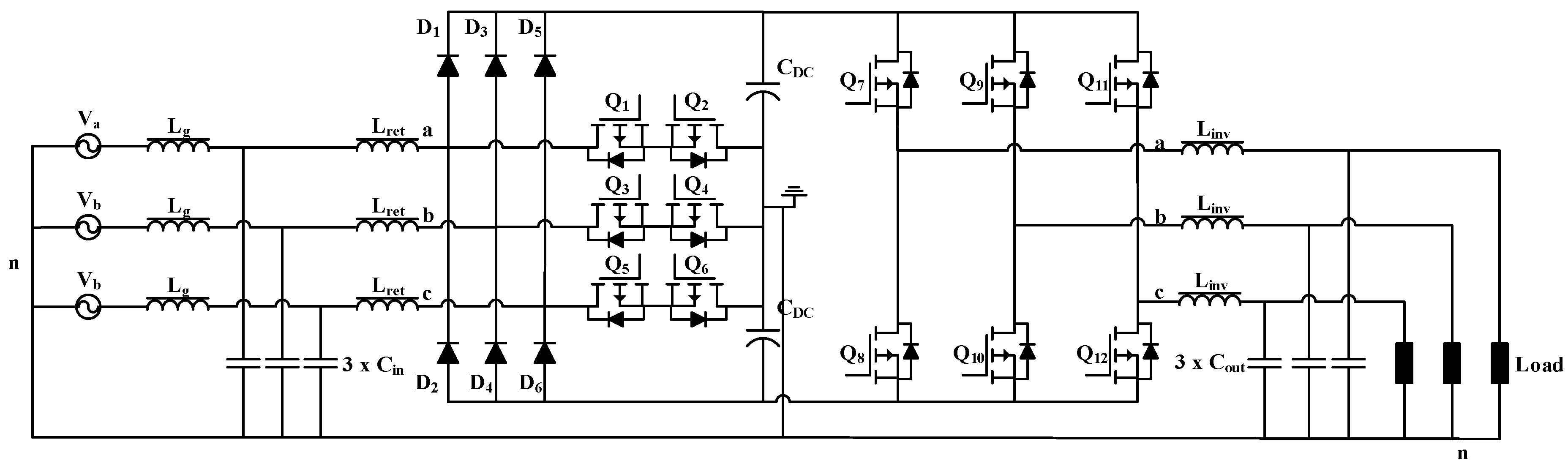
Table 1 summarizes the main specifications and design criteria for this AC-DC-AC conversion chain. An extensive topology and components comparison was done in [18] for two case scenarios, from the analyses carried out, it was decided to design the optimal converter that fits the specifications declared. The schematic diagram of the chosen topology is shown in Figure 1, it employs a Vienna Rectifier at the input and a 2-level inverter at the output. Silicon Carbide devices SCT3030AL ( to ) and STPSC40065C ( to ) will be used operating with switching frequencies up to 102 kHz in order to improve power density and achieve high efficiency. It was also verified in [18] that a Silicon IGBT-based converter would be unpractical due to very high switching losses when operating at 100 kHz. The converter will operate with slightly different switching frequencies for the rectifier and for the inverter to avoid resonances and oscillations.
3. Hardware Design
This section is focused on the design of the main hardware components. The following topics are addressed: Thermal design (loss estimation and heat sink sizing), inductor design ( and ), and capacitors sizing (DC link and filter capacitors).
3.1. Thermal Design
Despite being a good first step for comparison and topology choice, the estimation of switch losses through the use of datasheet’s switching energy curves, as done in [18], is not accurate. The manufacturer does not clearly state the conditions under which the double pulse test was performed, the measuring equipment used, and the inductance of the switching loop are not reported. Some researchers have published recent works reporting big differences between the energy curves available in the datasheet and experimental curves verified in real prototypes [19,20,21].
The cited works used experimental setups to measure the switching energies to, then, be able to use this data in the converter loss estimation. However, most of the time it is necessary that the designer can estimate the losses of a converter without the need to perform an experimental procedure.
Thus, this work will use a simulation approach to estimate the energy curves of the SiC MOSFET and, afterward, estimate the losses. The simulation will be done in Spice via SImetrix software using the Spice model of the SCT3030AL transistor provided by the manufacturer. However, the simulation must be done in order to model a more realistic condition of operation considering the inductances of the power loop and transistors leads. These inductances exert great influence on the transistor’s switching and can make it slower. Thus, a more realistic simulation was performed including the parasitic inductances of decoupling capacitors, transistors, and PCB tracks. The simulation diagram can be seen in Figure 2.
The simulation was performed for current values between 0 and 75 A, and the energy curves obtained were plotted in Figure 3 with the curves provided by the manufacturer.
By analyzing the graph, it is possible to notice that the inclusion of the parasite inductances greatly affects the switching losses, which reaffirms the need to minimize these inductances. The difference reaches about 70% to the maximum current point. In addition, it is noted that when the current is close to zero, the switching energy is not zero, this is due to insufficient energy to discharge and charge the parasitic capacitances of the transistors. In this way, the switching will only occur after the end of the dead time, when the complementary key will be closed, realizing the abrupt charge and discharge of the MOSFETs output capacitances. Therefore, when the current is close to zero, the energy lost in the switching corresponds to the energy stored in the parasitic capacitances.
The total losses were calculated, using the method of loss estimation described in [22] and the curves obtained by simulation, and are shown in Table 2 for the rectifier and in Table 3 for the inverter. Since the SiC Schottky diode has negligible reverse recovery, its switching losses were considered zero.
From the estimation of losses it is possible to size the heatsink for cooling the converter. Two identical heatsinks have been chosen for use, one for the rectifier switches and one for cooling the inverter switches, the part number is P 16 from Semikron with standard length of 100 mm.
The thermal resistance () of this heatsink, when subjected to an air flow of 6 m/s in its fins, is 0.175 ℃/W. A Sil-Pad 2000 thermal interface was used whose thermal resistance () is 0.23 ℃/W. As the junction-case () thermal resistance of the diode and the MOSFET are respectively 0.6 ℃/W and 0.44 ℃/W, the temperatures at the junctions of the transistors can be calculated through the thermal models of the Figure 4 and Figure 5.
The temperatures were calculated and are shown in Table 4, it was considered an ambient temperature of 40 ℃. As can be seen, the none of the junction temperatures of the semiconductor devices exceeded the maximum operating limit of 175 ℃. Thus, the thermal design developed is considered adequate.
3.2. Inductor Design
The input and output inductors are responsible for filtering the harmonic components at the switching frequency. The inductor design involves calculating the inductance required to obtain a particular ripple, choice of magnetic core material, and winding design.
The required inductance value can be calculated by the following generic equation [23]:
where n is a variable that depends on the number of levels, for 2-level converters and for 3-level converters . Thus, it is possible to calculate the value for input and output inductances. Firstly for the rectifier:
Then, a similar calculation is made for the inverter:
It was decided to use relatively high ripple values to reduce the inductance required and improve system dynamics.
For the choice of magnetic material, only alloy powder cores were considered because they are often more suitable for operation at high currents and mid switching frequency range. It was decided to fix the core size and choose the material based on its losses and its cost. Table 5 shows the main characteristics of the evaluated cores.
Core losses can be calculated using the formula proposed by Steinmetz, which is an empirical expression that is adjusted to the loss data by choosing 3 coefficients supplied by the manufacturers or obtained from curves that can also be supplied by the manufacturers. The equation can be written as:
where , , and are the Steinmetz coefficients which depend on the characteristics of the material, f is the operating frequency, is the peak value of the flux density, and is the volume of the magnetic core.
However, this empirical equation is obtained from the application of sinusoidal flux densities. The flux density imposed on magnetic materials of static converters usually has non-sinusoidal waveforms. For this reason, many researchers have proposed improvements to the Steinmetz equation to take into account the application of non-sinusoidal waveforms. Some of these proposals are Modified Steinmetz Equation-MSE [24], Generalized Steinmetz Equation-GSE [25], improved Generalized Steinmetz Equation-iGSE [26], and improved-improved Generalized Steinmetz Equation-iGSE [27].
Some papers have presented accurate results when iGSE or iGSE are used to estimate core losses, with errors between the experimental and theoretical results lower than 10% [26,27,28,29]. The difference between iGSE and iGSE is the fact that iGSE includes the relaxation effects due to DC levels of the flux density. However, the flux-density waveforms of the converters in this work do not show DC levels, so the use of iGSE is sufficient for calculating core losses. The formula for using the iGSE method is given below:
with being determined by:
Although the iGSE has been demonstrated to be accurate, the computational routine proposed by its authors has two drawbacks: the first is the computational complexity of the algorithm that must scan the flux density data vector to perform a loops separation, the second is the generation of the flux density data vector which, if done by simulation, can spend considerable time.
For this reason, a method to accelerate the process of using iGSE has been proposed in [30]. The method consists of the deduction of the closed-form solution of the excitation waveform. In this way, it is possible to perform the iGSE calculations only with the converter input data (RMS voltage, RMS current, switching frequency, magnetic core data), i.e., without the need for simulation or complex algorithms, making it ideal for use in design optimization softwares for inductors. The authors in [30] made the deductions in the case of a single-phase Bridgeless PFC converter, and can also be applied to 3-level Vienna rectifiers. An extension was made to cover a 2-level inverter and was used in this work to calculate core losses.
Then, the losses were calculated for the four cores evaluated as a function of the number of turns for . Figure 6 shows the results of calculating the core losses. First, it can be seen that the core with the highest losses is the XFlux, so it is discarded from selection. Then, the higher the number of turns the lower the difference between the losses of the High Flux core and the high-cost MPP core. Moreover, MPP and Kool M cores have the disadvantage of low saturation flux density, Figure 6 shows that, even with few turns, these cores saturate due to the high current of the inverter. Therefore, the core High Flux will be chosen for the rectifier and inverter inductors.
The number of turns used in the rectifier and inverter inductors will be 26 and 33, respectively. With this amount of turns it is possible to achieve the required inductance. To compose the windings, 38 AWG25 gauge copper wires will be used in parallel. Considering that the copper resistivity at 100 ℃ is [31], the dc winding resistance will be 6.1 m and 7.8 m for the rectifier and inverter inductors, respectively. The estimated copper losses and core losses are shown in Table 6, only the fundamental component was considered to calculate copper losses, core losses were considered constant and independent of the load.
3.3. Capacitor Sizing
The sizing of the DC link capacitor takes into account the ripple criteria. For the DC link capacitor, the worst case occurs when the inverter feeds an unbalanced load, the higher the unbalance the greater the ripple. Thus, it is possible to calculate the needed capacitance when the neutral current and the ripple are given [4]:
where is the output voltage peak value and is the neutral current peak value.
It was decided to use 4 electrolytic capacitors of 560 F/400 V, manufactured by EPCOS part number B43644B9567M000, in parallel, totaling a capacitance of 2240 F for each group.
Then, the output LC filter capacitor will be sized based on the attenuation criteria, this filter is required to attenuate harmonic components close to the switching frequency. It is a second order and has attenuation of 40 dB per decade from the cutoff frequency, so the cutoff frequency, , will be defined as less than one-tenth of the switching frequency, which will guarantee a 100-fold attenuation in the amplitude of the harmonics. Therefore, the capacitor value can be determined by:
Thus, it was decided to use three capacitors of 2.2 F/400 V in parallel, totaling a capacitance of 6.6 F, the capacitors are manufactured by Panasonic part number ECQ-E4225KF.
The input LCL filter is formed by the grid inductance (), rectifier inductance () and input capacitance (). Several researchers have published works where the central subject is the design and modeling of LCL filters using different methodologies and criteria [32,33,34,35]. However, the grid inductance changes depending on the electrical network, the equipment is expected to operate in facilities where the grid inductance varies from 64.19 H to 1.28 mH, which allows a short circuit power from 10 to 200 times the power of the equipment. As the rectifier inductance and the grid inductance were already defined, it remains only to size the input capacitor.
One of the criteria defined in [32] recommends to allocate the resonance frequency between ten times the grid frequency (600 Hz) and half the switching frequency (51 kHz). The resonant frequency of an LCL filter can be calculated by the equation:
By rearranging the terms of the Equation (9) and allocating the resonance frequency at 15 kHz, it is possible to obtain a range of values for the capacitor.
In this way, it was decided to use two 2.2 F/400 V capacitors in parallel, totalizing a capacitance of 4.4 F, the capacitors are manufactured by Panasonic part number ECQ-E4225KF.
4. Converter Control
This section addresses the subject of converter control. Although the control strategy is not the main focus of this paper, a closed loop control system is needed for proper converter operation. The goals of the control are:
- Power factor correction;
- Keep the input current and output voltage at low THD (<15%);
- Regulate output voltage;
- Rejection of load disturbances;
- Synchronize input and output voltages;
- Regulate DC link voltage at 400 V.
The control strategy was implemented with the micro-controller TMS320F28379D which has two processing cores, one core was used to control the rectifier and the second was used to control the inverter.
Figure 7 shows the rectifier’s control system. The first three loops, more internal, control the currents in the inductors of each phase, the control action is composed by the response of a proportional controller (P) together with the feed-forward of the input voltage. The outermost and slower loop is responsible for maintaining constant voltage on the DC link, the use of a proportional-integral compensator (PI) is sufficient to guarantee zero error in a steady state, the output of this loop multiplied by three-phase sine-wave voltages generates the reference for the internal current loops. The PLL (Phase Locked Loop) is used to generate these three-phase voltages, this decouples the reference of possible distortions present in the input voltages, improving the quality of the synthesized current [36].
Figure 8 shows the inverter’s control system. It is composed by three voltage loops, one for each phase, the control action is composed by the response of a proportional-integral controller (PI) together with the feed-forward of the reference voltage. The PLL is used to generate reference voltages that are synchronized with the input voltages.
5. Prototype Analysis and Experimental Results
In this section, the developed AC-DC-AC converter will be analyzed in terms of power density and the experimental results will be presented. The efficiency and compliance with norms in terms of power factor and THD will be validated.
5.1. Prototype
Figure 9 shows a photo of the designed prototype, it employs a Vienna Rectifier at the input and a 2-level inverter at the output and uses Silicon Carbide devices operating with switching frequencies up to 102 kHz. This converter is intended for use in highly efficient three-phase double conversion UPS applications and is rated at 10 kW.
The currents of the inductors, the input voltages, the output voltages, and the DC link voltages were measured and fed into a LaunchPad Development Kit TMS320F28379D to implement the closed loop PWM control.
To highlight the benefits of using Silicon Carbide devices, the developed SiC-based prototype was compared to a commercial Silicon IGBT-based UPS with the same specifications. Figure 10 shows a size comparison between the two pieces of equipment, it is possible to observe that the SiC-based prototype is much smaller than the IGBT-based UPS. However, the prototype is not a complete product and does not have batteries, protections, nor enclosure, hence one can say that the comparison is not equitable. To establish a fair comparison, this work will focus on the hardware components designed and performance.
Table 7 shows a performance and power density comparison with regard to the converter as a whole and to individual components.
Silicon Carbide switches enabled the construction of an highly efficient prototype, the 450 W reduction on losses allows a saving of about 1380 USD, considering that the prototype would operate continuously during one year in Germany. Less losses also means lighter cooling systems, the mass of heat sink and fans were reduced by 50% and 72.5%, respectively.
Additionally, the high switching frequency operation capability of SiC devices allows the size reduction of passive components such as inductors and capacitors, Figure 11 and Figure 12, these components had a reduction of about 90% in mass and volume. The prototype measures 17 L and 7.13 kg, which means a power density of 0.588 kW/L and a power-to-mass ratio of 1.4 kW/kg.
5.2. Experimental Results
The first result is the steady state behavior of the converter. Figure 13 shows the main input and output electrical variables at nominal load measured with the power analyzer YOKOGAWA WT1800. It is possible to note that these waveforms respect a sinusoidal shape that will lead to high power quality, that affirmation is confirmed by measuring the THD of the input current and the output voltage whose values are 3.8% and 3.2%, respectively. The measured rectifier power factor was 0.997 at rated load. The input current THD is kept low, even for cases of light load, as shown in Figure 14 and Table 8. The steady state performance under nonlinear was also evaluated, a nonlinear load rated at 3.3 kVA, Power factor 0.62, and Crest factor 3.4 was connected on phase A, Figure 15 demonstrates the obtained result, the output voltage was kept at low distortion yielding a THD of 5.3%. The obtained results validate the steady state operation and complies with the IEC-62040-3 and the IEC-61000-3-12.
Next, the converter dynamic behavior under load changes was evaluated. Figure 16 shows the DC link voltage, output voltage, input current and output current under two load variations, one negative 25% load step, and a positive 25% load step. For both cases, the control loop responds rapidly and the overvoltage/voltage dip has an absolute value lower than 20 V.
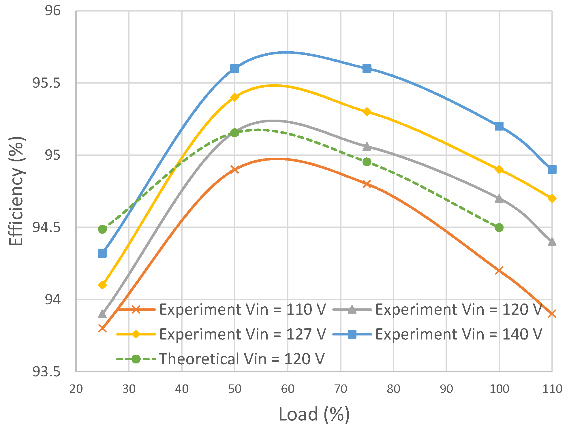
Then, Figure 17 shows an efficiency evaluation as a function of the output power and the input voltage. The experimental efficiency is over 95% for most operating points, meeting the design requirements, and reach a peak of 95.6% when the input voltage is 140 V (phase-neutral) and the load is 75% of the nominal power. The difference between experimental and theoretical efficiency is lower than 1% when the input voltage is 120 V. Although the converter is rated at 10 kW, it was experimentally verified that it can operate continuously with 10% overload.
Figure 18 shows the temperature distribution for both inverter and rectifier inductors operating at rated load. The temperature of the rectifier inductors is lower for two reasons: The rectifier 3-level configuration that lowers the excursion of magnetic flux density and consequently reduces core losses, the second reason is the positioning of the fans, which generates an air flow that passes first through the rectifier and exits at the inverter. The observed maximum temperatures are 54.8 ℃ and 85.8 ℃ for the rectifier and inverter inductors, respectively. In this way, the inductors operate with a good safety margin, since the maximum operating temperature of the material High Flux is 200 ℃.
Due to the positioning of the electronic switches under the PCB, it is difficult to capture a thermal image that clearly shows the temperature distribution over all components. Since the inverter has less components, a lateral view was captured and is shown in Figure 19. It is possible to see that the maximum temperature is about 126 ℃ , which validates the thermal model and the loss model for the inverter.
6. Conclusions
This work has made an extensive coverage on the design of a three phase AC-DC-AC converter for UPS applications using Silicon Carbide. The focus was the hardware design which includes thermal design, inductor design, and filter capacitors sizing.
Since the manufacturer’s datasheet does not completely characterize the SiC MOSFET for real operating conditions, a simulation method to estimate switching energy curves was proposed to incorporate parasitic inductance into switching behavior, allowing for more accurate losses prediction. An accurate losses prediction avoids oversizing or undersizing of the heatsink.
Also, it was shown that the inductors have a great impact on the UPS efficiency and cost. The inductor design method achieved inductors with a moderate compromise between losses, cost, and size.
The design procedure described in this work has achieved an highly efficient electronic converter for double conversion UPS that complies with the IEC-62040-3. If higher efficiency is required, the designer can reduce the switching frequency and/or improve the inductor by changing its core material, although this can increase cost.
Experimental results and comparisons have shown that Silicon Carbide devices can offer the possibility of higher frequency operation while enhances the system efficiency, thus, the obtained converters have smaller passive components and smaller heatsinks. UPS that employs these wide bandgap devices will offer energy savings and reduce costs with cooling systems and equipment accommodation.
Author Contributions
Conceptualization, W.C.A., L.M.F.M. and P.C.C.; methodology, W.C.A.; software, W.C.A.; validation, W.C.A., L.M.F.M. and P.C.C.; formal analysis, W.C.A.; investigation, W.C.A., L.M.F.M. and P.C.C.; resources, P.C.C.; data curation, W.C.A.; writing—original draft preparation, W.C.A.; writing—review and editing, L.M.F.M. and P.C.C.; visualization, W.C.A.; supervision, L.M.F.M. and P.C.C.; project administration, P.C.C.; funding acquisition, P.C.C.
Funding
This study was financed in part by the Coordenação de Aperfeiçoamento de Pessoal de Nível Superior—Brasil (CAPES)—Finance Code 001.
Conflicts of Interest
The authors declare no conflict of interest. The funders had no role in the design of the study; in the collection, analyses, or interpretation of data; in the writing of the manuscript, or in the decision to publish the results.
Abbreviations
The following abbreviations are used in this manuscript:
| UPS | Uninterruptible Power Supplies |
| SiC | Silicon Carbide |
| GaN | Gallium Nitride |
| WBG | Wide Bandgap |
| MOSFET | Metal Oxide Semiconductor Field Effect Transistor |
| PWM | Pulse Width Modulation |
| PCB | Printed Circuit Board |
| THD | Total Harmonic Distortion |
| PLL | Phase Locked Loop |
References
- SourceOECD. World energy balances. In IEA World Energy Statistics and Balances (Database); IEA: Paris, France, 2015. [Google Scholar]
- Bekiarov, S.B.; Emadi, A. Uninterruptible power supplies: classification, operation, dynamics, and control. In Proceedings of the APEC Seventeenth Annual IEEE Applied Power Electronics Conference and Exposition, Dallas, TX, USA, 10–14 March 2002; Volume 1, pp. 597–604. [Google Scholar]
- Karve, S. Three of a kind. IEE Rev. 2000, 46, 27–31. [Google Scholar] [CrossRef]
- Fraser, M.; Manning, C.; Wells, B. Transformerless four-wire PWM rectifier and its application in AC-DC-AC converters. IEE Proc. Electr. Power Appl. 1995, 142, 410–416. [Google Scholar] [CrossRef]
- Kim, E.H.; Kwon, J.M.; Kwon, B.H. Transformerless three-phase on-line UPS with high performance. IET Power Electron. 2009, 2, 103–112. [Google Scholar] [CrossRef]
- Da Silva, S.O.; Donoso-Garcia, P.F.; Cortizo, P.C.; Seixas, P.F. A three-phase line-interactive UPS system implementation with series-parallel active power-line conditioning capabilities. IEEE Trans. Ind. Appl. 2002, 38, 1581–1590. [Google Scholar] [CrossRef]
- Wei, B.; Guerrero, J.M.; Vásquez, J.C.; Guo, X. A Circulating-Current Suppression Method for Parallel-Connected Voltage-Source Inverters With Common DC and AC Buses. IEEE Trans. Ind. Appl. 2017, 53, 3758–3769. [Google Scholar] [CrossRef] [Green Version]
- Komatsu, K.; Yatsu, M.; Miyashita, S.; Okita, S.; Nakazawa, H.; Igarashi, S.; Takahashi, Y.; Okuma, Y.; Seki, Y.; Fujihira, T. New IGBT modules for advanced neutral-point-clamped 3-level power converters. In Proceedings of the 2010 International IEEE Power Electronics Conference (IPEC), Sapporo, Japan, 21–24 June 2010; pp. 523–527. [Google Scholar]
- Lee, T.; Kinoshita, M.; Sanada, K. High-efficiency large-capacity uninterruptible power supply using bidirectional-switch-based NPC multilevel converter. In Proceedings of the 2011 IEEE 8th International Conference on Power Electronics and ECCE Asia (ICPE & ECCE), Jeju, Korea, 30 May–30 June 2011; pp. 2100–2105. [Google Scholar]
- Dong, D.; Chen, L.; Li, H.; Chen, M.; Xu, D. Design of hybrid ac-dc-ac topology for uninterruptible power supply. In Proceedings of the 2015 IEEE 2nd International Future Energy Electronics Conference (IFEEC), Taipei, Taiwan, 1–4 November 2015; pp. 1–5. [Google Scholar]
- Biela, J.; Schweizer, M.; Waffler, S.; Kolar, J.W. SiC versus Si—Evaluation of potentials for performance improvement of inverter and DC–DC converter systems by SiC power semiconductors. IEEE Trans. Ind. Electron. 2011, 58, 2872–2882. [Google Scholar] [CrossRef]
- Millan, J.; Godignon, P.; Perpina, X.; Pérez-Tomás, A.; Rebollo, J. A survey of wide bandgap power semiconductor devices. IEEE Trans. Power Electron. 2014, 29, 2155–2163. [Google Scholar] [CrossRef]
- Armstrong, K.O.; Das, S.; Cresko, J. Wide bandgap semiconductor opportunities in power electronics. In Proceedings of the 2016 IEEE 4th Workshop on Wide Bandgap Power Devices and Applications (WiPDA), Fayetteville, AR, USA, 7–9 November 2016; pp. 259–264. [Google Scholar]
- Cougo, B.; Schneider, H.; Meynard, T. High current ripple for power density and efficiency improvement in wide bandgap transistor-based buck converters. IEEE Trans. Power Electron. 2015, 30, 4489–4504. [Google Scholar] [CrossRef]
- Chen, C.; Chen, Y.; Tan, Y.; Fang, J.; Luo, F.; Kang, Y. On the Practical Design of a High Power Density SiC Single-Phase Uninterrupted Power Supply System. IEEE Trans. Ind. Inform. 2017, 13, 2704–2716. [Google Scholar] [CrossRef]
- Luo, C.; Wang, X.; Jiang, T.; Feng, R.; Xin, H.; Li, H. Experimental study of a SiC MOSFET based single phase inverter in UPS applications. In Proceedings of the 2016 IEEEEnergy Conversion Congress and Exposition (ECCE), Milwaukee, WI, USA, 18–22 September 2016; pp. 1–6. [Google Scholar]
- Boroyevich, D.; DiMarino, C. Is SiC a Game Changer? In Proceedings of the Tutorial talks Southern Power Electronics Conference, Fortaleza, Brazil, 29 November 2015. [Google Scholar]
- Alves, W.C.; Morais, L.M.; Cortizo, P.C. Design of an efficient hybrid AC-DC-AC converter using silicon carbide for ups applications: A comparison. In Proceedings of the 2017 Brazilian Power Electronics Conference (COBEP), Juiz de Fora, Brazil, 19–22 November 2017; pp. 1–6. [Google Scholar]
- Sathler, H.; Cougo, B. Improvement of the modified opposition method used for accurate switching energy estimation of WBG transistors. In Proceedings of the 2017 IEEE 5th Workshop on Wide Bandgap Power Devices and Applications (WiPDA), Albuquerque, NM, USA, 30 October–1 November 2017; pp. 308–315. [Google Scholar] [CrossRef]
- Anthon, A.; Hernandez, J.C.; Zhang, Z.; Andersen, M.A. Switching investigations on a SiC MOSFET in a TO-247 package. In Proceedings of the IECON 2014-40th Annual Conference of the IEEE Industrial Electronics Society, Dallas, TX, USA, 29 October–1 November 2014; pp. 1854–1860. [Google Scholar]
- Laird, I.; Yuan, X.; Scoltock, J.; Forsyth, A. A Design Optimisation Tool for Maximising the Power Density of 3-Phase DC-AC Converters Using Silicon Carbide (SiC) Devices. IEEE Trans. Power Electron. 2017, 33, 2913–2932. [Google Scholar] [CrossRef]
- Cota, A.P.; Abrantes, R.C.; Cortizo, P.C.; Santana, R.A.; Padrão, W.C. Comparison of three 3-phase converter topologies for ups applications. In Proceedings of the 2015 IEEE 13th Brazilian Power Electronics Conference and 1st Southern Power Electronics Conference (COBEP/SPEC), Fortaleza, Brazil, 29 November–2 December 2015; pp. 1–6. [Google Scholar]
- Teodorescu, R.; Liserre, M.; Rodriguez, P. Grid Converters for Photovoltaic and Wind Power Systems; John Wiley & Sons: Hoboken, NJ, USA, 2011; Volume 29. [Google Scholar]
- Reinert, J.; Brockmeyer, A.; De Doncker, R.W. Calculation of losses in ferro-and ferrimagnetic materials based on the modified Steinmetz equation. IEEE Trans. Ind. Appl. 2001, 37, 1055–1061. [Google Scholar] [CrossRef]
- Li, J.; Abdallah, T.; Sullivan, C.R. Improved calculation of core loss with nonsinusoidal waveforms. In Proceedings of the Conference Record of the 2001 IEEE Industry Applications Conference, Thirty-Sixth IAS Annual Meeting, Chicago, IL, USA, 30 September–4 October 2001; Volume 4, pp. 2203–2210. [Google Scholar]
- Venkatachalam, K.; Sullivan, C.R.; Abdallah, T.; Tacca, H. Accurate prediction of ferrite core loss with nonsinusoidal waveforms using only Steinmetz parameters. In Proceedings of the 2002 IEEE Workshop on Computers in Power Electronics, Mayaguez, PR, USA, 3–4 June 2002; pp. 36–41. [Google Scholar]
- Muhlethaler, J.; Biela, J.; Kolar, J.W.; Ecklebe, A. Improved core-loss calculation for magnetic components employed in power electronic systems. IEEE Trans. Power Electron. 2012, 27, 964–973. [Google Scholar] [CrossRef]
- Mühlethaler, J.; Kolar, J.W.; Ecklebe, A. Loss modeling of inductive components employed in power electronic systems. In Proceedings of the 8th International Conference on Power Electronics—ECCE Asia, Jeju, Korea, 30 May–3 June 2011; pp. 945–952. [Google Scholar]
- Muller, S.; Keller, M.; Maier, M.; Parspour, N. Comparison of Iron Loss Calculation Methods for Soft Magnetic Composite. In Proceedings of the 2017 IEEE 14th Brazilian Power Electronics Conference, Juiz de Fora, Brazil, 19–22 November 2017; pp. 1–6. [Google Scholar]
- Jacoboski, M.J.; Lange, A.D.B.; Heldwein, M.L. Closed-Form Solution for Core Loss Calculation in Single-Phase Bridgeless PFC Rectifiers Based on the iGSE Method. IEEE Trans. Power Electron. 2017, 33, 4599–4604. [Google Scholar] [CrossRef]
- Serway, R.A.; Jewett, J.W. Physics for Scientists and Engineers With Modern Physics; Cengage Learning: Boston, MA, USA, 2018. [Google Scholar]
- Liserre, M.; Blaabjerg, F.; Hansen, S. Design and control of an LCL-filter-based three-phase active rectifier. IEEE Trans. Ind. Appl. 2005, 41, 1281–1291. [Google Scholar] [CrossRef]
- Araújo, S.V.; Engler, A.; Sahan, B.; Antunes, F.L.M. LCL filter design for grid-connected NPC inverters in offshore wind turbines. In Proceedings of the 7th Internatonal Conference on Power Electronics, Daegu, Korea, 22–26 October 2007; pp. 1133–1138. [Google Scholar]
- Reznik, A.; Simoes, M.G.; Al-Durra, A.; Muyeen, S. LCL filter design and performance analysis for grid-interconnected systems. IEEE Trans. Ind. Appl. 2014, 50, 1225–1232. [Google Scholar] [CrossRef]
- Wang, T.C.; Ye, Z.; Sinha, G.; Yuan, X. Output filter design for a grid-interconnected three-phase inverter. In Proceedings of the 2003 IEEE 34th Annual Power Electronics Specialist Conference, Acapulco, Mexico, 15–19 June 2003; Volume 2, pp. 779–784. [Google Scholar]
- Morais, L.; Santos Filho, R.; Cortizo, P.; Seleme, S.; Garcia, P.D.; Seixas, P. Pll-based repetitive control applied to the single-phase power factor correction using boost converter. In Proceedings of the 35th Annual Conference of IEEE Industrial Electronics, Porto, Portugal, 3–5 November 2009; pp. 737–742. [Google Scholar]
Figure 1.
Proposed AC-DC-AC converter.

Figure 2.
Diagram of the simulation performed in Spice to extract the switching energy curves, with addition of parasite inductances.
Figure 2.
Diagram of the simulation performed in Spice to extract the switching energy curves, with addition of parasite inductances.

Figure 3.
Comparison of the energy curves obtained by simulation and the curves disclosed in the datasheet of the device SCT3030AL. Conditions: = 18 V/0 V, = 400 V, = 0 Ω.
Figure 3.
Comparison of the energy curves obtained by simulation and the curves disclosed in the datasheet of the device SCT3030AL. Conditions: = 18 V/0 V, = 400 V, = 0 Ω.

Figure 4.
Equivalent thermal model for dissipation of the heat generated by the rectifier switches.

Figure 5.
Equivalent thermal model for dissipation of the heat generated by the inverter switches.

Figure 6.
Core losses comparison of the inductors of the rectifier and inverter for four materials as a function of number of turns. The arrows indicate an occurrence of core saturation.
Figure 6.
Core losses comparison of the inductors of the rectifier and inverter for four materials as a function of number of turns. The arrows indicate an occurrence of core saturation.

Figure 7.
Control strategy applied for the rectifier.

Figure 8.
Control strategy applied for the inverter.

Figure 9.
Designed prototype.

Figure 10.
Size comparison between the developed SiC-based prototype and a commercial IGBT-based Uninterruptible Power Supply (UPS) with the same specifications.
Figure 10.
Size comparison between the developed SiC-based prototype and a commercial IGBT-based Uninterruptible Power Supply (UPS) with the same specifications.

Figure 11.
Size comparison between filter inductors for the developed SiC-based prototype and for a commercial IGBT-based UPS with the same specifications.
Figure 11.
Size comparison between filter inductors for the developed SiC-based prototype and for a commercial IGBT-based UPS with the same specifications.

Figure 12.
Size comparison between filter capacitors for the developed SiC-based prototype and for a commercial IGBT-based UPS with the same specifications.
Figure 12.
Size comparison between filter capacitors for the developed SiC-based prototype and for a commercial IGBT-based UPS with the same specifications.

Figure 13.
Measured input and output waveforms in steady state at nominal power, the input voltage is 120 V (phase-neutral).
Figure 13.
Measured input and output waveforms in steady state at nominal power, the input voltage is 120 V (phase-neutral).

Figure 14.
Measured input and output waveforms in steady state at 25% load, the input voltage is 127 V (phase-neutral).
Figure 14.
Measured input and output waveforms in steady state at 25% load, the input voltage is 127 V (phase-neutral).

Figure 15.
Experimental results supplying a nonlinear load. CH1: DC Link voltage, CH2: Output voltage, CH3: Input current, CH4: Output current.
Figure 15.
Experimental results supplying a nonlinear load. CH1: DC Link voltage, CH2: Output voltage, CH3: Input current, CH4: Output current.

Figure 16.
Dynamic behavior of the converter under load changes (a) −25% load step (b) 25% load step. CH1: DC Link voltage, CH2: Output voltage, CH3: Input current, CH4: Output current.
Figure 16.
Dynamic behavior of the converter under load changes (a) −25% load step (b) 25% load step. CH1: DC Link voltage, CH2: Output voltage, CH3: Input current, CH4: Output current.

Figure 17.
Efficiency measured with the power analyzer YOKOGAWA WT1800 for different input voltages and load conditions.
Figure 17.
Efficiency measured with the power analyzer YOKOGAWA WT1800 for different input voltages and load conditions.

Figure 18.
Thermal images for inductors operating at nominal power (a) Rectifier (b) Inverter.

Figure 19.
Thermal image for the inverter operating at nominal power, this lateral view shows only and on phase C.
Figure 19.
Thermal image for the inverter operating at nominal power, this lateral view shows only and on phase C.


Table 1.
Main specifications and design criteria.
| Especification | Value |
|---|---|
| Output Power () | 10 kW |
| Output voltage phase-neutral () | 127 V |
| Output current () | 26.25 A |
| Input Power () | 11 kW |
| Input voltage phase-neutral () | 127 V +/− 10% |
| Input current () | 32 A (worst case) |
| DC link voltage () | 400 V |
| Grid frequency () | 60 Hz |
| Inverter’s switching frequency () | 101.34 kHz |
| Rectifier’s switching frequency () | 102 kHz |
| Ambient temperature () | 40 ℃ |
| Max. junction temperature () | 150 ℃ |
| Max. inverter current ripple() | 40% of peak current |
| Max. rectifier current ripple () | 30% of peak current |
| Max. DC link ripple () | 5% of |
| Efficiency () | 95% |
Table 2.
Losses calculated for the rectifier operating at 102 kHz switching frequency.
| Per Diode STPSC40065C | Per MOSFET SCT3030AL | Total Losses | |||||
|---|---|---|---|---|---|---|---|
| Load | |||||||
| 25% | 2.10 W | 0 | 2.10 W | 0.36 W | 3.70 W | 4.06 W | 36.96 W |
| 50% | 4.70 W | 0 | 4.70 W | 1.40 W | 7.10 W | 8.50 W | 79.20 W |
| 75% | 7.70 W | 0 | 7.70 W | 3.40 W | 11.30 W | 14.70 W | 134.40 W |
| 100% | 11.50 W | 0 | 11.50 W | 5.70 W | 16.60 W | 22.30 W | 202.80 W |
Table 3.
Losses calculated for the inverter operating at 101.34 kHz switching frequency.
| Per MOSFET SCT3030AL | Total Losses | |||
|---|---|---|---|---|
| Load | ||||
| 25% | 0.83 W | 9.2 W | 10.03 W | 60.2 W |
| 50% | 3.09 W | 16.91 W | 20 W | 120 W |
| 75% | 6.7 W | 26.4 W | 33.1 W | 198.6 W |
| 100% | 12.55 W | 37.55 W | 50.1 W | 300.6 W |
| Rectifier | ||||
|---|---|---|---|---|
| Temperature | 40 ℃ | 90.4 ℃ | 85.0 ℃ | 75.5 ℃ |
| Inverter | ||||
| Temperature | 40 ℃ | 126.2 ℃ | NA | 104.1 ℃ |
Table 5.
Characteristics of the magnetic cores considered.
| Material | High Flux | XFlux | MPP | Kool M |
|---|---|---|---|---|
| Composition | FeNi | FeSi | FeNiMo | FeSiAl |
| Part Number | C058090A2 | 0078090A7 | C055090A2 | 0077090A7 |
| 60 | 60 | 60 | 60 | |
| (nH/Turn) | 86 ± 8% | 86 ± 8% | 86 ± 8% | 86 ± 8% |
| (T) | 1.5 | 1.6 | 0.8 | 1.0 |
| (℃) | 200 | 200 | 200 | 200 |
| OD (mm) | 47.63 | 47.63 | 47.63 | 47.63 |
| ID (mm) | 27.88 | 27.88 | 27.88 | 27.88 |
| HT (mm) | 16.2 | 16.2 | 16.2 | 16.2 |
| (mm) | 116 | 116 | 116 | 116 |
| (mm) | 134 | 134 | 134 | 134 |
| (mm) | 610 | 610 | 610 | 610 |
| (cm) | 15.6 | 15.6 | 15.6 | 15.6 |
| (mm) | 66.4 | 66.4 | 66.4 | 66.4 |
| (mW/cm³) | 0.055 | 0.034 | 0.155 | 0.026 |
| 1.32 | 1.332 | 1.12 | 1.29 | |
| 2.22 | 1.825 | 2.05 | 2.01 | |
| Cost (USD) | 6.60 | 2.21 | 32.42 | 5.19 |
Table 6.
Losses calculated for inductors.
| Per Rectifier’s Inductor | Per Inverter’s Inductor | Total | |||
|---|---|---|---|---|---|
| Load | |||||
| 25% | 4.99 W | 0.29 W | 11.3 W | 0.33 W | 50.7 W |
| 50% | 4.99 W | 1.16 W | 11.3 W | 1.33 W | 56.3 W |
| 75% | 4.99 W | 2.62 W | 11.3 W | 3.00 W | 65.7 W |
| 100% | 4.99 W | 4.66 W | 11.3 W | 5.34 W | 78.9 W |
Table 7.
Performance and power density comparison between the developed SiC-based prototype and a commercial IGBT-based Uninterruptible Power Supply (UPS) with the same specifications.
Table 7.
Performance and power density comparison between the developed SiC-based prototype and a commercial IGBT-based Uninterruptible Power Supply (UPS) with the same specifications.
| Parameter | Commercial UPS | Prototype | Difference |
|---|---|---|---|
| IGBT-Based 15 kHz | SiC-Based 100 kHz | ||
| Nominal point losses | 950 W | 500 W | −47.3% |
| Hardware * mass | 21.36 kg | 6.88 kg | −67.8% |
| Hardware * volume | 11.9 L | 4.38 L | −63.2% |
| Filter capacitance () | 90 F | 6.6 F | −92.7% |
| Filter capacitor mass () | 226 g | 23 g | −89.8% |
| Filter capacitor volume () | 200 cm³ | 22 cm³ | −89% |
| Filter inductance () | 290 H | 66 H | −77.2% |
| Filter inductor mass () | 1588 g | 255 g | −83.9% |
| Filter inductor volume () | 464.8 cm³ | 35.3 cm³ | −92.4% |
| Heat sink mass | 9400 g | 4700 g | −50% |
| Fan mass | 1090 g | 300 g | −72.5% |
* Hardware considers the sum of all components sized in the paper, that is, all capacitors, all inductors, fans and heat sinks. It does not account for batteries, protections, auxiliary circuits, PCB nor steel case.
Table 8.
Input and output power quality measurements under linear load condition.
| Load | Rectifier Power Factor | Input Current THD (%) | Output Voltage THD (%) |
|---|---|---|---|
| 25% | 0.98 | 11.2 | 1.4 |
| 50% | 0.994 | 5.7 | 1.8 |
| 75% | 0.996 | 4.5 | 2.7 |
| 100% | 0.997 | 3.8 | 3.2 |
© 2018 by the authors. Licensee MDPI, Basel, Switzerland. This article is an open access article distributed under the terms and conditions of the Creative Commons Attribution (CC BY) license (http://creativecommons.org/licenses/by/4.0/).
Share and Cite
MDPI and ACS Style
Alves, W.C.; Morais, L.M.F.; Cortizo, P.C. Design of an Highly Efficient AC-DC-AC Three-Phase Converter Using SiC for UPS Applications. Electronics 2018, 7, 425. https://doi.org/10.3390/electronics7120425
AMA Style
Alves WC, Morais LMF, Cortizo PC. Design of an Highly Efficient AC-DC-AC Three-Phase Converter Using SiC for UPS Applications. Electronics. 2018; 7(12):425. https://doi.org/10.3390/electronics7120425
Chicago/Turabian StyleAlves, Wendell C., Lenin M. F. Morais, and Porfirio C. Cortizo. 2018. "Design of an Highly Efficient AC-DC-AC Three-Phase Converter Using SiC for UPS Applications" Electronics 7, no. 12: 425. https://doi.org/10.3390/electronics7120425
Note that from the first issue of 2016, this journal uses article numbers instead of page numbers. See further details here.