An Efficient Equalizing Method for Lithium-Ion Batteries Based on Coupled Inductor Balancing


Department of Electrical Energy, Metals, Mechanical Constructions and Systems, Gent University, 9052 Gent, Belgium
*
Author to whom correspondence should be addressed.
Electronics 2019, 8(2), 136; https://doi.org/10.3390/electronics8020136
Submission received: 14 January 2019
/
Revised: 22 January 2019
/
Accepted: 24 January 2019
/
Published: 29 January 2019
(This article belongs to the Section Semiconductor Devices)
Abstract
:This article developed a coupled inductor balancing method to overcome cell voltage variation among cells in series, for Lithium Ion (Li-ion) batteries in Electrical Vehicles (EV). For an "eight cells in series" example, the developed balance circuit has four inductors, one magnetic circuit with one winding per two cells, and one control switch per cell, as compared to the traditional inductor-based equalizer that needs N-1 inductors and magnetic circuits for N number of cells and more switches. Therefore, ultimately, a more efficient, cost-effective circuit and low bill of materials (BOM) will be built up. All switches are logic-level N-Channel metal-oxide-semiconductor field-effect transistors (MOSFETs) and they are controlled by a pair of complementary signals in a synchronous trigger pattern. In the proposed topology, less components and fast equalization are achieved compared to the conventional battery management system (BMS) technique for electrical vehicles based on the inductor balancing method. This scheme is suitable for fast equalization due to the inductor-based balancing method. The inductors are made with a well-chosen winding ratio and all are coupled with one magnetic core with an air gap. Theoretical derivation of the proposed circuit was well-presented, and numerical simulation relevant to the electrochemical storage devices was conducted to show the validity of the proposed balance circuit. A complete balance circuit was built to verify that the proposed circuit could resolve imbalance problems which existed inside battery modules.
1. Introduction
Electrical vehicles (EV) can achieve low pollution and low noise compared to gasoline-powered vehicles; therefore, the demand for electrical vehicles has increased during the last decade. The total cost of electrical vehicles depends on many aspects, but the most expensive part of it is the cost of the batteries. To achieve reasonable longevity, a battery management system is required to reach the best performance. Li-ion batteries are widely used in many applications, such as electrical vehicles, electric bikes, and uninterruptible power supplies (UPS) due to their advantages, such as high energy density, low self-discharge rates, compact volume, lower weight, and higher discharge current without effects on memory and a long life cycle [1,2,3,4]. To match the voltage with the application and to lower the cable losses, Li-ion batteries’ cells are connected in series configuration. However, due to the charging/discharging cycles, the voltages of the cells will differ and poses a potential failure. These unavoidable differences are due to chemical and electrical characteristics, such as production tolerance, asymmetrical degradation with aging, internal impedance, and uneven temperature distribution [5,6]. The capacity of a battery is gradually reduced due to erosion, passivation, out-gassing, temperature, decomposition of materials, and changes on the electrode surface during its operation [7,8]. The problems of the capacity and resistance variation are increased by different cell aging. In fact, this imbalance results in a reduction in the charge storage potential and the lifetime of the battery pack. Voltage imbalance is a major factor that deteriorates the performance and reliability of the battery pack because of the decrease in the usable capacity due to the low-voltage battery cell and the fire risk due to overcharging. Overcharging may cause a reduction in capacity, deterioration, and destruction, and deep discharge may also cause the cell to be permanently deteriorated. Thus, battery equalizers are needed in order to ensure that all cells in a series-connected battery string are fully charged or discharged. Many battery equalizers have been proposed during the last few years [9,10,11,12]. These applications are divided into a passive balancing technique and an active balancing technique. The passive balancing technique connects resistors and switches to each battery cell and dissipates energy using the resistor, while the active balancing technique is used to overcome the problem of energy loss and equalizes voltages of battery cells by transferring charge from high-voltage battery cells to low-voltage battery cells, and is divided into two categories, such as charging-pass type and multi-winding transformer type [4,13,14,15].
The resistor cell balancing technique is a passive method that shunts the charging current around each cell if they become fully charged. They are based on removing the excess energy from the higher voltage cell by bypassing the current of the highest cell and waiting for the lower voltage cell to be at the same level. The resistors can be switched or used in a linear way, or dissipated in transistors, and the linear way generates less radio disturbance [16,17,18,19].
The capacitor balancing technique is an active method and can be brought into three categories: the switched capacitor, single switched capacitor, and double-tiered switched capacitor. This method utilizes capacitors as external energy storage devices for shuttling the energy between the pack cells. The first type has a simple control strategy because it only has two states it can work in for both the recharging and discharging operations [13,20]. The disadvantage of this method is the long equalization time. The second type needs only one capacitor to balance the cells, so a control strategy is needed to select the higher and the lower cell [14,21]. In the third type, the difference is that it uses two capacitors for energy shuttling. The advantage is that the second capacitor reduces the balancing time to a quarter of the time needed for the switched capacitor method [22,23]. However, a switched resonant switched capacitor balancing decreases the balancing time [24].
The inductor or transformer balancing techniques are active methods, where the operation principle is to move energy from a cell to another cell [25,26,27,28]. Due to the relatively high balancing current, they offer a shorter balancing executing time [29]. The transformer balancing may have a shorter balancing executing time. It also has disadvantages, such as high cost and magnetic losses. If all transistors are always switched at the secondary side, the leakage impedance determines the equalizing current for a voltage difference. It is not certain whether all secondary voltages are equal, due to the non-homogeneous field. More precise control is possible, but needs much more circuitry [4,15,30,31]. The switched inductor balancing method utilizes one inductor for transferring energy between the whole pack. The control system senses the voltage of the cells and selects the two cells which will be used for energy transferring, while the multi-switched inductor balancing needs an N-1 inductor for balancing N cells. They are featured by fast equalization time [26,32].
2. Conventional Inductor-Based Equalizer
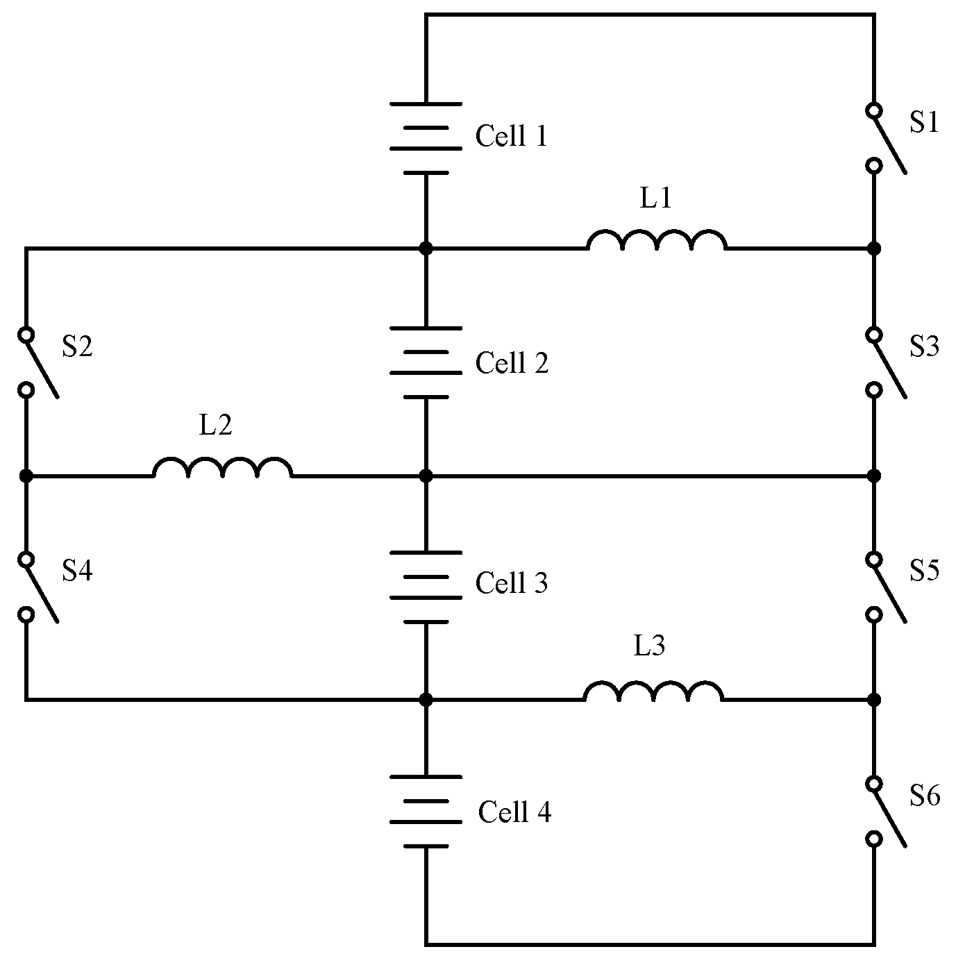
In this paper, the principle of active cell equalization based on the inductor balancing method is investigated. The conventional inductor-based equalizer uses an N-1 number of inductors in order to balance N cells by storing energy in the inductor. By controlling an on-and-off switch, the energy flows between the cells, as shown in Figure 1. The inductor balancing method has a high balancing current, thus it offers fast balancing time as compared to other methods. The operation principle can be divided into two stages.
In the first stage, the switches S, S, and S are turned on in order to store energy in the inductors from the cells, while the switches S, S, and S are turned off. In the second stage, switches S, S, and S are turned off, while S, S, and S will be turned on to transfer the stored energy in the inductors to the adjacent cells. The principle is to transfer the energy from the high-voltage cell to the lower one. This method has the disadvantage of a long balancing time, because energy is transferring from the first cell to the last, and it also contains the number of N-1 inductors for N number of cells and more switches, which ultimately causes more power loss, requires more components, and is not cost effective.
3. The Proposed Circuit Based on Coupled Inductor
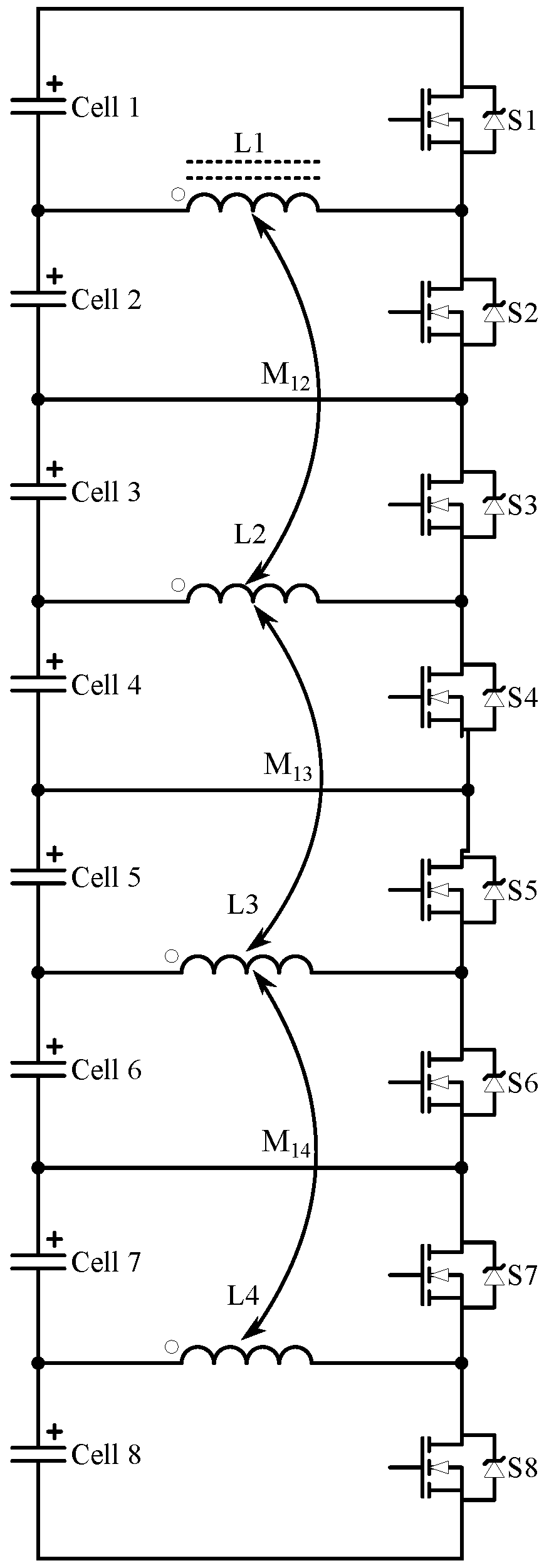
Some superior performance can be expected as the coupling property can be achieved by magnetic devices and not by capacitors. The proposed circuit uses one switch per cell, one winding per two cells and one magnetic circuit per battery. This means less components, cost effective, more efficient, and simple implementation. The block diagram of the proposed system is shown in Figure 2, which consist of eight battery cells and eight logic level N-Channel MOSFETs with body diodes and four coupled inductors.
The operation principle of the circuit can be divided in two main states.
(1) In Stage One, the switches S, S, S, S are turned on to store energy to the inductors, while the other switches are kept turned off. When switch S is on and S is off, the energy of Cell 1 will be transferred to Cell 2; therefore, the energy of Cell 1 will be stored in the inductor L. The inductor L can be expressed as:
where M is the self-inductance of Winding 1, and L is the leakage inductance of Winding 1. Similarly, M, M, M and L, L, L are the mutual inductance and leakage inductance of Windings 2, 3, and 4, respectively.
The inductor voltage of V can be expressed as:
where M is the mutual inductance between L and L, M is the mutual inductance between L and L, and M is the mutual inductance between L and L. Similarly, the inductor voltages L-L can be expressed as
where k = 2, 3, 4., i = 2, 3, 4., j = 1, 2, 3, 4.
and n = 3, 5, 7.
If inductors are symmetrical, but have different leakage inductances due to circuit layout, Equation (3) can be rewritten as:
Therefore, the inductor voltages for L-L can be rewritten as:
In the next mode, when the switches S, S, S, and S are turned off, the body diodes of the switches S, S, S, and S will turn on, and the energy stored in the inductors will be transferred to Cells 2, 4, 6, and 8. Therefore, the inductor voltages L can be expressed as:
Similarly, the inductor voltages L-L can be expressed as:
where k = 2, 3, 4., i = 2, 3, 4., j = 1, 2, 3, 4.
and n = 4, 6, 8.
Therefore, the inductor voltages for L-L can be rewritten as:
And then, it can be rewritten as:
The variation of inductor current when S is on can be expressed as:
For the second mode, when S is off and the body diode S is on the inductor voltage L based on Equation (7), it can be expressed as:
The variation of the inductor current when S is off and the body diode S is on can be expressed as:
As it can be known, in the steady state, the inductor current change is zero, thus:
According to Equation (17), the transfer function T can be written as:
(2) In Stage Two, the switches S, S, S, S are turned off, while the switches S, S, S, S are turned on to transfer the stored energy to the adjacent cells. In the first stage, the switch S is turned on and S is turned off, and the energy of cell will be stored in the inductor L.
In the next mode, when the switch S is off and the body diode of MOSFET S is on, the energy of the inductor L will be transferred to Cell 1. As discussed in the previous state, the principles are similar to Stage One, except that in this mode, Cell 2 acts as the input and the energy is transferred in the opposite direction. The principle for the other cells is the same.
Similarly, the transfer function T can be written as:
4. Simulation Results
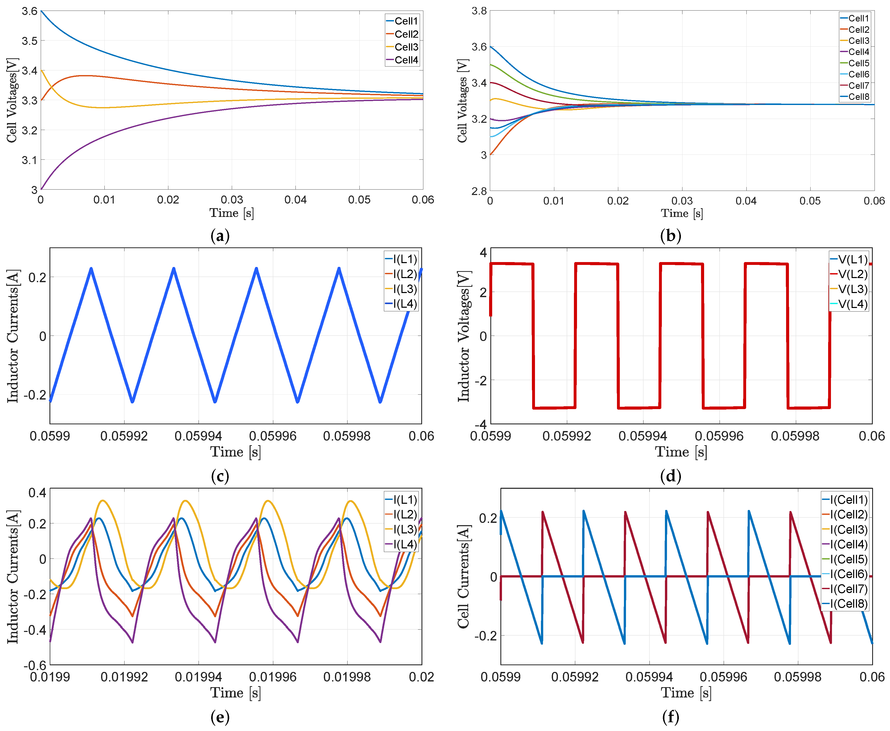
To verify the assumption, the model of the eight-battery cell is built in MATLAB/Simulink. In the simulation, eight capacitors with the value of 50 mF are used to model eight battery cells. The initial voltages are 3 V to 3.6 V in order to perform significant voltage differences of the cells in a battery pack. All the switches are N-channel MOSFETs with a body diode. A N-channel MOSFET is chosen due to the lower R in both the simulation and experimental setup. The switches are controlled by a pair of complementary signals in a synchronous trigger pattern with a switching frequency of 45 kHz and duty ratio of 45%, which is generated by the pulse generator. The inductors are modeled with a coupled inductor block in Simulink with a leakage inductance of 100 nH, magnetizing inductance of 20 H, and series resistance of 1 m. In order to compare between the conventional inductor-based balancing circuit and the proposed coupled inductor balancing circuit, the conventional inductor balancing with four cells was investigated in the simulation. Figure 3a shows the cell voltages of the conventional circuit [33,34], where it is evident that it has a longer equalization time compared to the proposed coupled inductor-balancing circuit.
In Figure 3a, the simulation result of the cell voltages of the proposed coupled inductor-balancing circuit with eight cells is presented. In the proposed topology, eight cells are considered. Due to the fact that by increasing the number of cells the equalization time will increase the proposed circuit has fast balancing time. Therefore, the proposed circuit is capable of balancing more than four cells in series with a fast equalization time. As it can be seen in the Figure, the proposed circuit has fast equalizing time compared with the conventional circuit. Figure 3b shows the simulation result of the coupled inductor currents. From the Figure, it is clear that the L-L currents have the same values in the steady state, which indicates no imbalances in the cells. In Figure 3c, the inductor voltages L-L are expressed. It is known that the average inductor voltage is zero in the period which is clear in the figure. Figure 3e,f shows the current waveforms of the coupled inductors in transient and current waveforms of the cells in the steady state, respectively.
5. Experimental Results
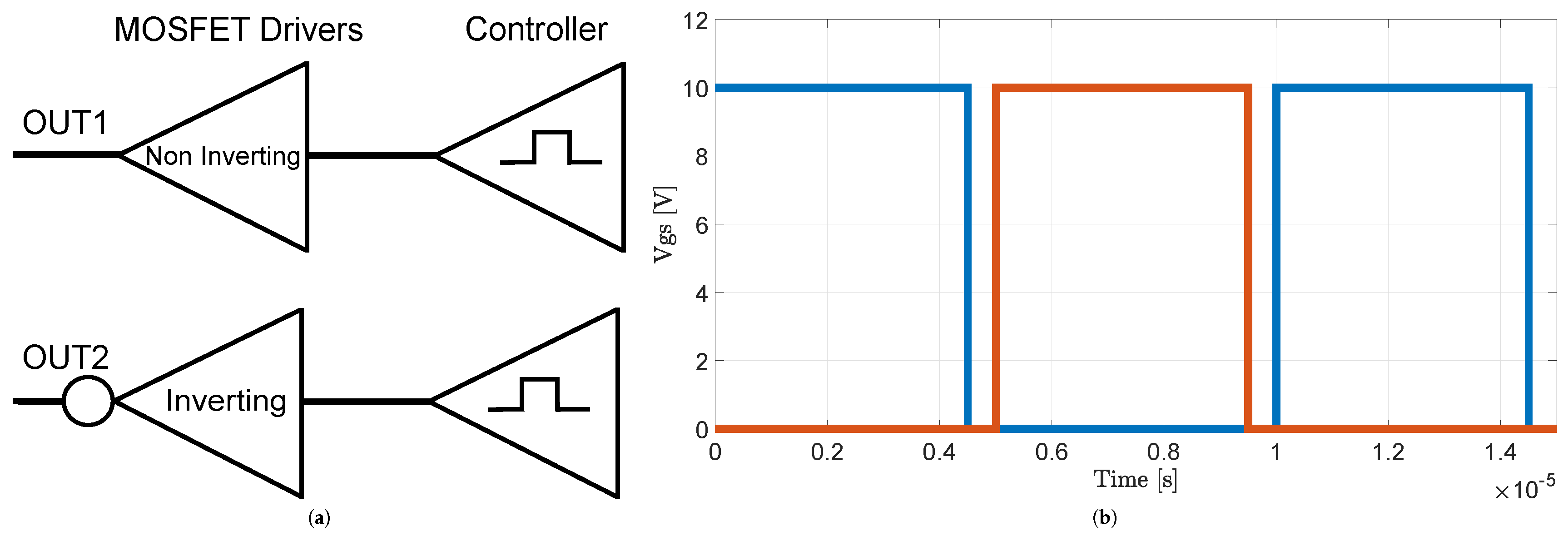
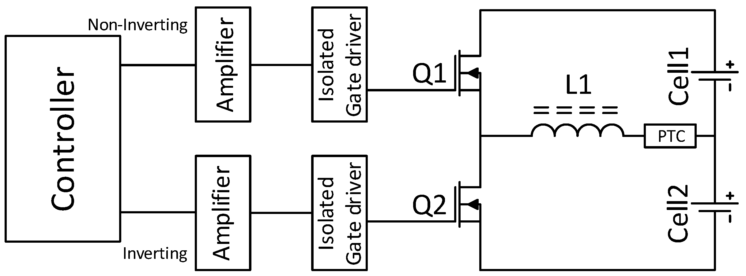
A prototype of the coupled inductor equalizer was implemented and tested. All the switches were logic-level N-Channel MOSFETs with body diodes, and were controlled by a pair of complementary signals in a synchronous trigger pattern generated by a microcontroller. The odd switches were controlled by a non-inverting MOSFET driver which was triggered by a microcontroller, and the even switches were controlled by an inverting MOSFET driver. In Figure 4a, the control block diagram of the proposed balancing circuit is presented. The coupled inductors were made with a well-chosen winding ratio, and were all coupled with one magnetic core with an air gap. In order to test the proposed topology, a prototype of the coupled inductor-balancing circuit was made to examine the feasibility of the system, as shown in Figure 2. This circuit equalized eight cells in a series. As it can be seen in Figure 4a, the gate to source voltage to the odd switches was applied to a non-inverting MOSFET driver, and the gate to source voltage to the even switches was applied to the inverting driver.
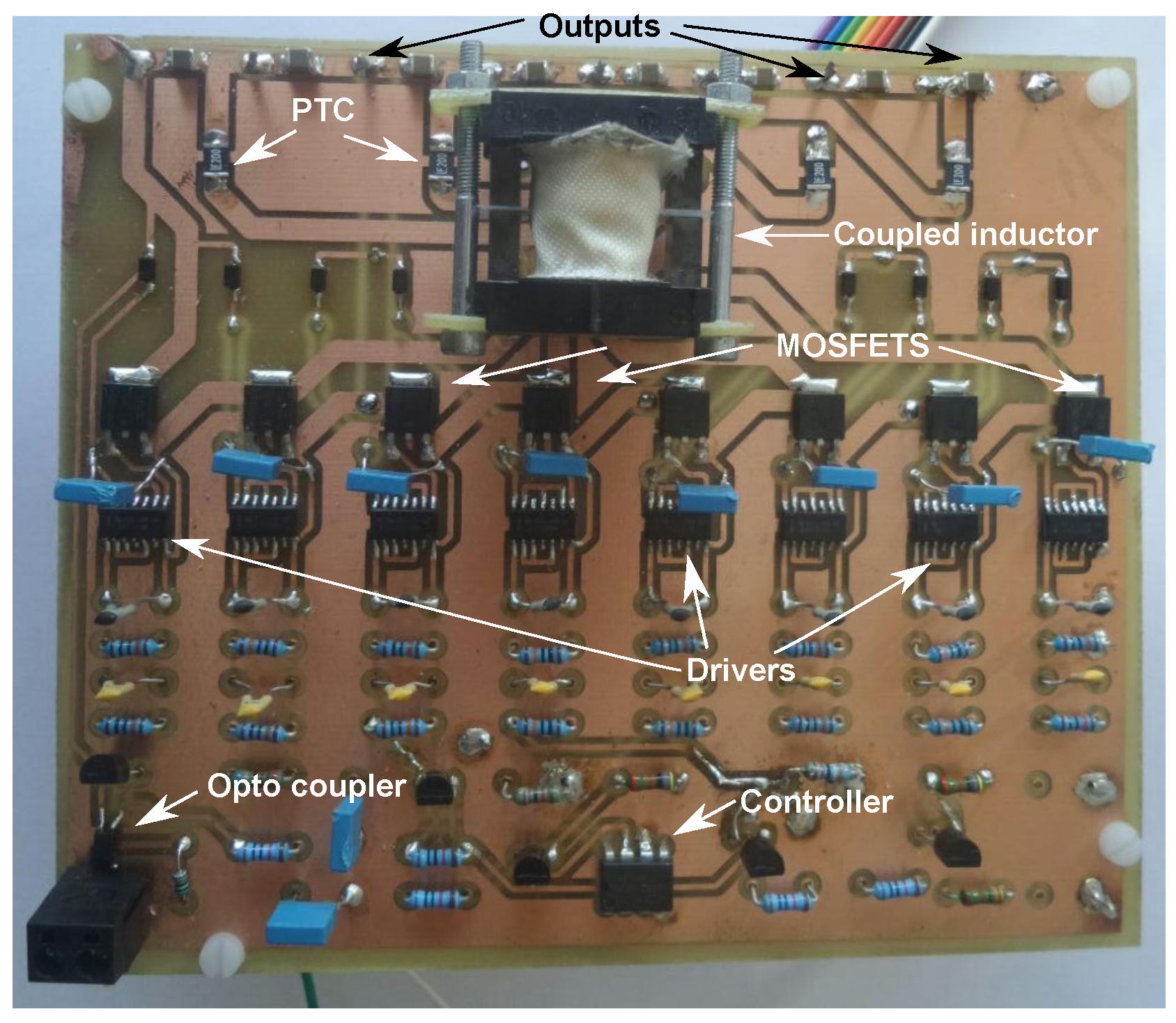
When the odd switches are triggered, the energy is stored in the inductor. In the next stage, when the even switches are triggered while the odd switches are turned off, the energy stored in the inductors circulate through the cells. The cells with a lower voltage absorb the energy and are charged to the nominal voltage. The desired gate to source the voltage (Vgs) to the MOSFETs with a 45% duty ratio is shown in Figure 4b. The switching frequency generated by microcontroller is 45.5 kHz, with a 45% duty cycle and 5% dead time to avoid shooting through between switches. The control circuit is isolated with optocoupler at the input for safety. All switches are logic-level N-Channel MOSFETs with lower R to decrease losses. The coupled inductor values are 10 for each inductor, and was measured by a LCR meter. In order to limit the inductor current, a resettable fuse (PTC) was implemented in the circuit in series with each inductor. The PTC was chosen in such a way that it limited the current up to 2A. The output was filtered with output filter capacitors with a value of 100 F. The schematic and the photograph of the PCB set up for the practical experiment is presented in Figure 5 and Figure 6, respectively.
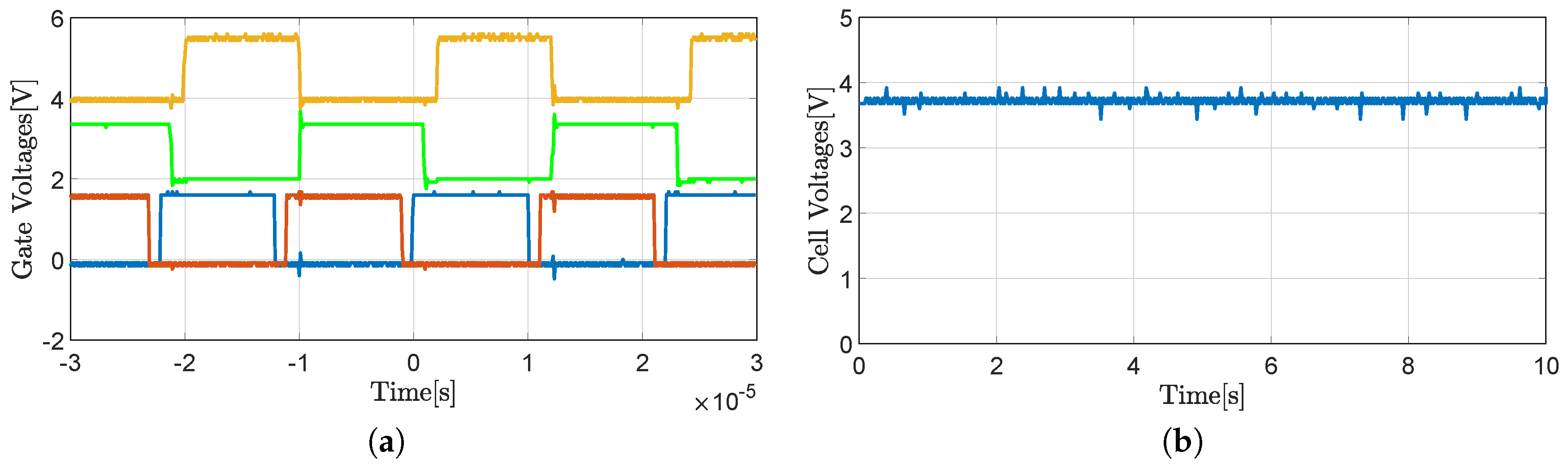
The output voltage of the driver (inverting and non-inverting), and the gate to the source voltage of the odd switches and gate to the source of the even switches is presented in Figure 7a. The blue is the non-inverting output of the driver, while the red is the inverting output. The orange waveform is the gate to the source of the odd switches, while the green is the gate to the source voltage of the even switches. As an example of the input voltages to the cells, Cell 1 is presented in Figure 7b.
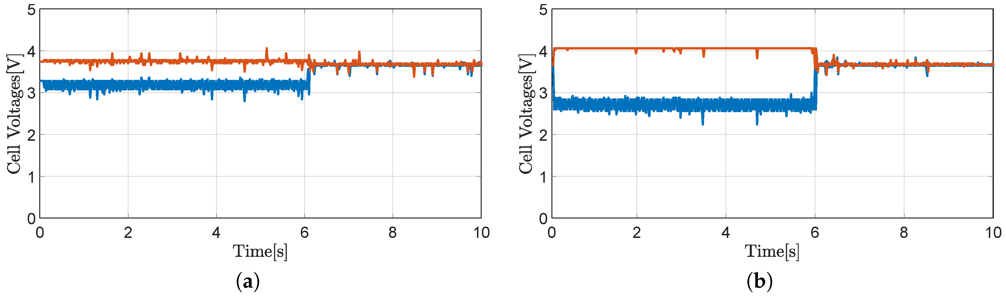
To verify the feasibility of the system, the imbalanced cell was considered to ensure that how the circuit will equalize it. In order to analyze that condition, cell was tested with 0.8 V and 1.2 V imbalance, respectively. In Figure 8a, the output voltage waveform of cell and cell with cell 0.8 V imbalanced is presented. The circuit was then tested with more imbalanced cells to test whether the circuit was robust with a higher number of imbalanced cells. The cell was considered to be imbalanced by 1.2 V in comparison to the other cells. The result of this is shown in Figure 8b, and it can be seen that the circuit was able to equalize with a fast speed in both cases.
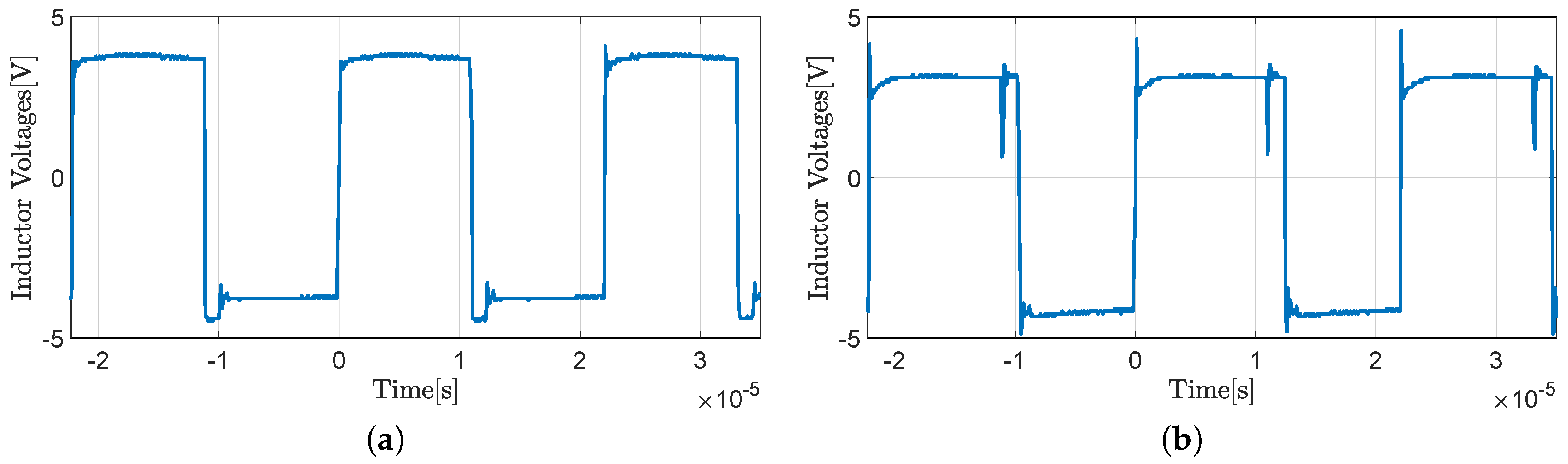
It has been known that the average voltage of the inductor is equal to zero. In Figure 9a, the inductor voltage value L is presented to verify this concept. In order to test between the balanced and imbalanced cell-inductor voltage, cell with 1.2 V imbalance was considered, and the inductor voltage L is shown in Figure 9b. All circuit parameter values of the proposed topology are presented in Table 1.
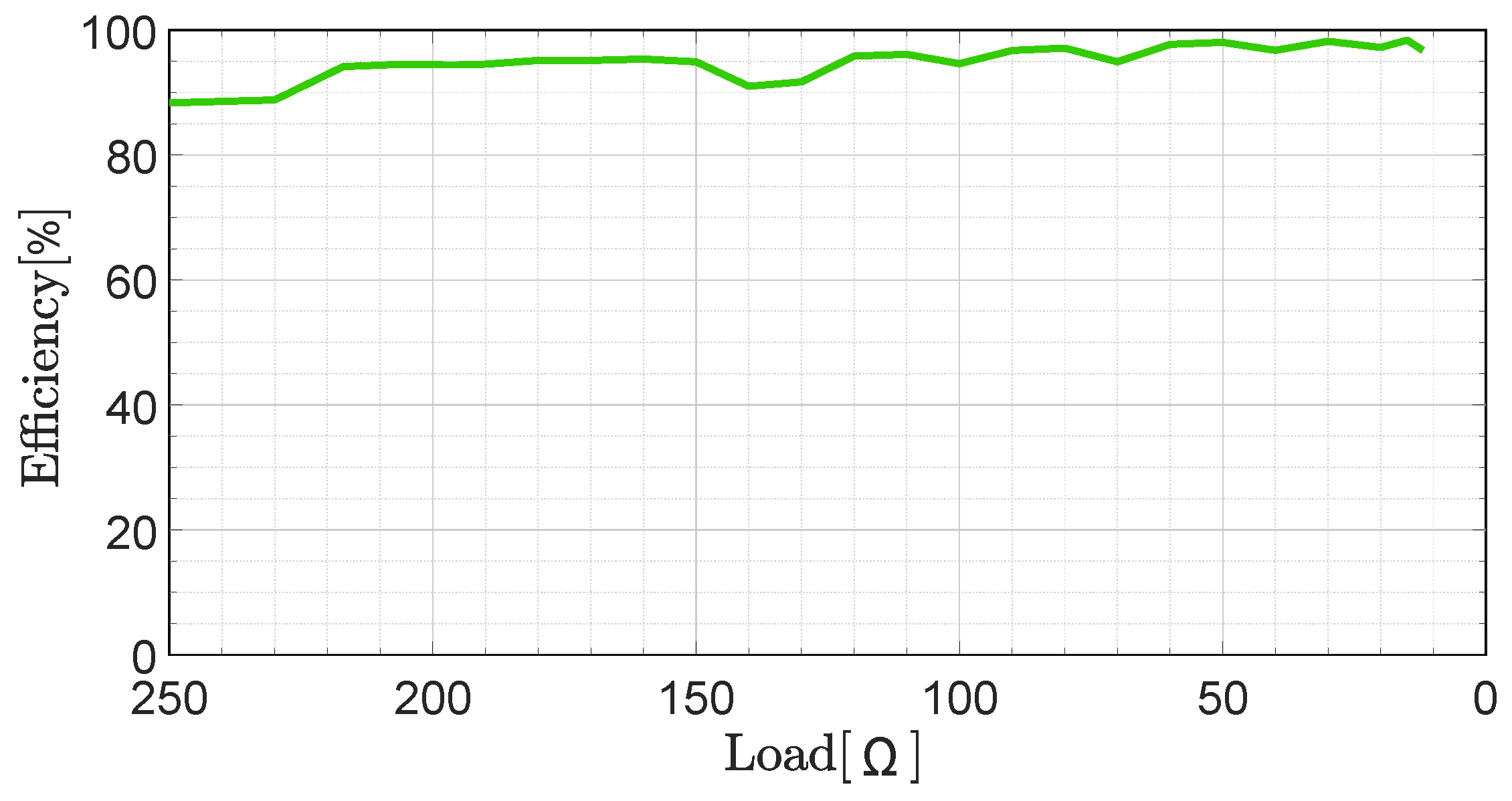
As an additional work, the efficiency of the coupled inductor circuit was calculated with different loads, and is presented in Figure 10. The loads were chosen from 250 to 12 in order to obtain significant data points to calculate the efficiency. It can be seen that with a 15 load, an efficiency of = 98.38% was achieved, which is a 2A-balancing current.
6. Conclusions
In this paper, the concept of an inductor-based balancing method was investigated. A number of cell-balancing methods were proposed. Alongside the existing equalization methods, an inductor-based balancing method has the advantages of fast balancing time compared to other existing methods. However, the conventional inductor circuit has slow balancing speed because the energy is transferred cell by cell. In order to overcome this problem, the proposed topology with a coupled inductor circuit was proposed, shown in Figure 1. This balancing method greatly improves the balancing time compared to the conventional inductor circuit, as shown in Figure 2. All the inductors were coupled with only one magnetic core with an air gap, and were made with a well-chosen winding ratio. The switches were logic-level N-Channel MOSFET, and were triggered by a microcontroller with a frequency of 45.5 kHz and duty cycle of 45% to avoid shoot-through between switches. The circuit was tested with different cell imbalances of 0.8 V and 1.2 V, respectively, to testify the viability of the system. In order to limit the charging currents, PTC was implemented for each inductor to limit the balancing current up to 2A. The experimental and simulation results were performed to verify the feasibility of the proposed topology.
Author Contributions
Conceptualization, A.F.M. and A.V.d.B.; methodology, A.F.M.; software, A.F.M.; validation, A.F.M.; formal analysis, A.F.M.; investigation, A.F.M.; resources, A.F.M.; data curation, A.F.M.; writing–original draft preparation, A.F.M.; writing–review and editing, A.F.M.; visualization, A.F.M.; supervision, A.V.d.B.
Funding
This research received no external funding.
Conflicts of Interest
The authors declare no conflict of interest.
References
- Lievre, A.; Sari, A.; Venet, P.; Hijazi, A.; Ouattara-Brigaudet, M.; Pelissier, S. Practical Online Estimation of Lithium-Ion Battery Apparent Series Resistance for Mild Hybrid Vehicles. IEEE Trans. Veh. Technol. 2016, 65, 4505–4511. [Google Scholar] [CrossRef]
- Lu, L.; Han, X.; Li, J.; Hua, J.; Ouyang, M. A review on the key issues for lithium-ion battery management in electric vehicles. J. Power Sources 2013, 226, 272–288. [Google Scholar] [CrossRef]
- Shang, Y.; Xia, B.; Zhang, C.; Cui, N.; Yang, J.; Mi, C. An automatic battery equalizer based on forward and flyback conversion for series-connected battery strings. In Proceedings of the 2017 IEEE Applied Power Electronics Conference and Exposition (APEC), Tampa, FL, USA, 26–30 March 2017; pp. 3218–3222. [Google Scholar]
- Moghaddam, A.F.; Mnati, M.; Sun, H.; Van den Bossche, A. Electric Vehicles Charging Concepts for Lithium Based Batteries. In Proceedings of the 2018 7th International Conference on Renewable Energy Research and Applications (ICRERA), Paris, France, 14–17 October 2018; pp. 397–401. [Google Scholar]
- Uno, M.; Tanaka, K. Single-Switch Cell Voltage Equalizer Using Multistacked Buck-Boost Converters Operating in Discontinuous Conduction Mode for Series-Connected Energy Storage Cells. IEEE Trans. Veh. Technol. 2011, 60, 3635–3645. [Google Scholar] [CrossRef]
- Uno, M.; Tanaka, K. Accelerated Charge–Discharge Cycling Test and Cycle Life Prediction Model for Supercapacitors in Alternative Battery Applications. IEEE Trans. Ind. Electron. 2012, 59, 4704–4712. [Google Scholar] [CrossRef]
- Hussein, A.A. Capacity Fade Estimation in Electric Vehicle Li-Ion Batteries Using Artificial Neural Networks. IEEE Trans. Ind. Appl. 2015, 51, 2321–2330. [Google Scholar] [CrossRef]
- Liu, X.; Zeng, G.; Yao, H.; Bo, D.; Xu, X. Research on the capacity fading characteristics of a Li-ion battery based on an equivalent thermal model. In Proceedings of the 2015 International Conference on Intelligent Computing and Internet of Things, Harbin, China, 17–18 January 2015; pp. 145–150. [Google Scholar]
- Ji, X.; Cui, N.; Shang, Y.; Zhang, C.; Sun, B. Modularized charge equalizer using multiwinding transformers for Lithium-ion battery system. In Proceedings of the 2014 IEEE Conference and Expo Transportation Electrification Asia-Pacific (ITEC Asia-Pacific), Beijing, China, 31 August–3 September 2014; pp. 1–5. [Google Scholar]
- Kim, C.; Kim, M.; Kim, Y.; Moon, G. A modularized charge equalizer using battery monitoring IC for series connected Li-Ion battery strings in an electric vehicle. IEEE Trans. Power Electron. 2013, 28, 3779–3787. [Google Scholar] [CrossRef]
- Lim, C.; Lee, K.; Ku, N.; Hyun, D.; Kim, R. A Modularized Equalization Method Based on Magnetizing Energy for a Series-Connected Lithium-Ion Battery String. IEEE Trans. Power Electron. 2014, 29, 1791–1799. [Google Scholar] [CrossRef]
- Park, H.; Kim, C.; Park, K.; Moon, G.; Lee, J. Design of a Charge Equalizer Based on Battery Modularization. IEEE Trans. Veh. Technol. 2009, 58, 3216–3223. [Google Scholar] [CrossRef]
- Kobzev, G.A. Switched-capacitor systems for battery equalization. In Proceedings of the 6th International Scientific and Practical Conference of Students, Post-graduates and Young Scientists. Modern Techniques and Technology, MTT’2000 (Cat. No. 00EX369), Tomsk, Russia, 3 March 2000; pp. 57–59. [Google Scholar]
- Moore, S.; Schneider, P. A Review of Cell Equalization Methods for Lithium Ion and Lithium Polymer Battery Systems. Available online: http://americansolarchallenge.org/ASC/wp-content/uploads/2013/01/SAE2001-01-0959.pdf (accessed on 29 January 2019).
- Kong, Z.-G.; Zhu, C.-B.; Lu, R.-G.; Cheng, S.-K. Comparison and evaluation of charge equalization technique for series connected batteries. In Proceedings of the 2006 37th IEEE Power Electronics Specialists Conference, Jeju, Korea, 18–22 June 2006; pp. 1–6. [Google Scholar]
- Kutkut, N.H.; Divan, D.M. Dynamic equalization techniques for series battery stacks. In Proceedings of the Intelec’96—International Telecommunications Energy Conference, Boston, MA, USA, 6–10 October 1996; pp. 514–521. [Google Scholar]
- Lindemark, B. Individual cell voltage equalizers (ICE) for reliable battery performance. In Proceedings of the Thirteenth International Telecommunications Energy Conference—INTELEC 91, Kyoto, Japan, 5–8 November 1991; pp. 196–201. [Google Scholar]
- Stuart, T.A.; Zhu, W. Fast equalization for large lithium ion batteries. IEEE Aerosp. Electron. Syst. Mag. 2009, 24, 27–31. [Google Scholar] [CrossRef] [Green Version]
- Zhang, X.; Liu, P.; Wang, D. The design and implementation of smart battery management system balance technology. J. Converg. Inf. Technol. 2011, 6, 108–116. [Google Scholar]
- Pascual, C.; Krein, P.T. Switched capacitor system for automatic series battery equalization. In Proceedings of the APEC 97—Applied Power Electronics Conference, Atlanta, GA, USA, 27 February 1997; pp. 848–854. [Google Scholar]
- Speltino, C.; Stefanopoulou, A.; Fiengo, G. Cell equalization in battery stacks through State of Charge estimation polling. In Proceedings of the 2010 American Control Conference, Baltimore, MD, USA, 30 June–2 July 2010; pp. 5050–5055. [Google Scholar]
- Baughman, A.C.; Ferdowsi, M. Double-Tiered Switched-Capacitor Battery Charge Equalization Technique. IEEE Trans. Ind. Electron. 2008, 55, 2277–2285. [Google Scholar] [CrossRef]
- Baughman, A.C.; Ferdowsi, M. Double-tiered capacitive shuttling method for balancing series-connected batteries. In Proceedings of the 2005 IEEE Vehicle Power and Propulsion Conference, Chicago, IL, USA, 7 September 2005; pp. 109–113. [Google Scholar]
- Moghaddam, A.F.; Van den Bossche, A. A Cell Equalization Method Based on Resonant Switched Capacitor Balancing for Lithium Ion Batteries. In Proceedings of the 2018 9th International Conference on Mechanical and Aerospace Engineering (ICMAE), Budapest, Hungary, 10–13 July 2018; pp. 337–341. [Google Scholar]
- Imtiaz, A.M.; Khan, F.H.; Kamath, H. A low-cost time shared cell balancing technique for future lithium-ion battery storage system featuring regenerative energy distribution. In Proceedings of the 2011 Twenty-Sixth Annual IEEE Applied Power Electronics Conference and Exposition (APEC), Fort Worth, TX, USA, 6–11 March 2011; pp. 792–799. [Google Scholar]
- Moo, C.S.; Hsieh, Y.C.; Tsai, I.S.; Cheng, J.C. Dynamic charge equalisation for series-connected batteries. IEEE Proc. Electr. Power Appl. 2003, 150, 501–505. [Google Scholar] [CrossRef]
- Shin, J.; Seo, G.; Chun, C.; Cho, B. Selective flyback balancing circuit with improved balancing speed for series connected Lithium-ion batteries. In Proceedings of the 2010 International Power Electronics Conference—ECCE ASIA, Sapporo, Japan, 21–24 June 2010; pp. 1180–1184. [Google Scholar]
- Einhorn, M.; Roessler, W.; Fleig, J. Improved Performance of Serially Connected Li-Ion Batteries with Active Cell Balancing in Electric Vehicles. IEEE Trans. Veh. Technol. 2011, 60, 2448–2457. [Google Scholar] [CrossRef]
- Moghaddam, A.F.; Van den Bossche, A. An Active Cell Equalization Technique for Lithium Ion Batteries Based on Inductor Balancing. In Proceedings of the 2018 9th International Conference on Mechanical and Aerospace Engineering (ICMAE), Budapest, Hungary, 10–13 July 2018; pp. 274–278. [Google Scholar]
- Li, S.; Mi, C.C.; Zhang, M. A High-Efficiency Active Battery-Balancing Circuit Using Multiwinding Transformer. IEEE Trans. Ind. Appl. 2013, 49, 198–207. [Google Scholar] [CrossRef]
- Moghaddam, A.F.; Van den Bossche, A. Multi-Winding Equalization Technique for Lithium Ion Batteries for Electrical Vehicles. In Proceedings of the 2018 7th International Conference on Renewable Energy Research and Applications (ICRERA), Paris, France, 14–17 October 2018; pp. 139–143. [Google Scholar]
- Phung, T.H.; Crebier, J.; Chureau, A.; Collet, A.; Nguyen, V. Optimized structure for next-to-next balancing of series-connected lithium-ion cells. In Proceedings of the 2011 Twenty-Sixth Annual IEEE Applied Power Electronics Conference and Exposition (APEC), Fort Worth, TX, USA, 6–11 March 2011; pp. 1374–1381. [Google Scholar]
- Lin, J.C.M. Development of a new battery management system with an independent balance module for electrical motorcycles. Energies 2017, 10, 1289. [Google Scholar] [CrossRef]
- Lin, J.C.M. Development of a globally active balance module with range extension effect. IET Electr. Syst. Transp. 2016, 10, 154–160. [Google Scholar] [CrossRef]
Figure 1.
Conventional inductor-based equalizer circuit.

Figure 2.
The proposed circuit based on coupled inductor balancing.

Figure 3.
(a) Cell voltages of the conventional inductor-balancing circuit; (b) Cell voltage waveforms of the proposed coupled inductor-balancing circuit; (c) current waveforms of the coupled inductors in the steady state; (d) voltage waveforms of the coupled inductor-balancing circuit in the steady state L-L; (e) current waveforms of the coupled inductors in the transient state; (f) current waveforms of the cells in the steady state.

Figure 4.
(a) Control block diagram; (b) MOSFET gate to source voltage with 5% dead time.

Figure 5.
The schematic of the proposed circuit.

Figure 6.
A photograph of the PCB set up for the practical experiment.

Figure 7.
(a) The output voltage of the driver and gate to the source voltage of the switches; (b) the input voltage of the cells.
Figure 7.
(a) The output voltage of the driver and gate to the source voltage of the switches; (b) the input voltage of the cells.

Figure 8.
(a) Inductor voltage waveform (L) with cell 0.8 V imbalance; (b) inductor voltage waveform (L) with cell 1.2 V imbalance.
Figure 8.
(a) Inductor voltage waveform (L) with cell 0.8 V imbalance; (b) inductor voltage waveform (L) with cell 1.2 V imbalance.

Figure 9.
(a) Cell and cell output voltage waveform with cell 0.8 V imbalance; (b) cell and cell output voltage waveform with cell 1.2 V imbalance.
Figure 9.
(a) Cell and cell output voltage waveform with cell 0.8 V imbalance; (b) cell and cell output voltage waveform with cell 1.2 V imbalance.

Figure 10.
Efficiency of the circuit with different loads.


Table 1.
parameters values.
| L, L, L, L | H |
| MOSFET (R) | 104 m max |
| Switching frequency | 45.5 kHz |
| Duty cycle | 45% |
| Cell voltages | 3.7 V nominal |
| Dead time | 5% |
| Number of cells | 8 cells |
| PTC | 2 A |
| Output filter capacitors | 100 |
© 2019 by the authors. Licensee MDPI, Basel, Switzerland. This article is an open access article distributed under the terms and conditions of the Creative Commons Attribution (CC BY) license (http://creativecommons.org/licenses/by/4.0/).
Share and Cite
MDPI and ACS Style
Farzan Moghaddam, A.; Van den Bossche, A. An Efficient Equalizing Method for Lithium-Ion Batteries Based on Coupled Inductor Balancing. Electronics 2019, 8, 136. https://doi.org/10.3390/electronics8020136
AMA Style
Farzan Moghaddam A, Van den Bossche A. An Efficient Equalizing Method for Lithium-Ion Batteries Based on Coupled Inductor Balancing. Electronics. 2019; 8(2):136. https://doi.org/10.3390/electronics8020136
Chicago/Turabian StyleFarzan Moghaddam, Ali, and Alex Van den Bossche. 2019. "An Efficient Equalizing Method for Lithium-Ion Batteries Based on Coupled Inductor Balancing" Electronics 8, no. 2: 136. https://doi.org/10.3390/electronics8020136
Note that from the first issue of 2016, this journal uses article numbers instead of page numbers. See further details here.