Article

Efficient Iterative Process Based on an Improved Genetic Algorithm for Decoupling Capacitor Placement at Board Level

1
UAq EMC Laboratory, Dept. of Industrial and Information Engineering and Economics, University of L’Aquila, 67100 L’Aquila, Italy
2
Zuken GmbH, 33104 Paderborn, Germany
*
Author to whom correspondence should be addressed.
Electronics 2019, 8(11), 1219; https://doi.org/10.3390/electronics8111219
Submission received: 30 September 2019 / Revised: 22 October 2019 / Accepted: 23 October 2019 / Published: 24 October 2019

Abstract

:
To reduce the noise created by a power delivery network, the number, the value of decoupling capacitors and their arrangement on the board are critical to reaching this goal. This work deals with specific improvements, implemented on a genetic algorithm, which used for the optimization of the decoupling capacitors in order to obtain the frequency spectrum of the input impedance in different positions on the network, below previously defined values. Measurements are performed on a specifically manufactured board in order to validate the effectiveness of the proposed algorithm and the optimization results obtained for a specific example board.

1. Introduction

The miniaturization of the devices is nowadays a consolidated trend in the industry development of the electronic products that are also boosted by the spread of the Internet of Thing (IoT) paradigm [1], as well as by other new technologies, such as 5G [2] and high-speed digital transmission [3]. This reduction of the overall geometrical dimensions is greatly implemented at the printed circuit board (PCB) level and, with the proper scaling factor, at package and chip level respectively. At the clear advantages of device (or part of them) miniaturization are associated a good number of engineering challenges such an increased design and manufacturing complexity, increasing of power density with the related heat dissipation problems [4]. The electromagnetic interferences (EMI) among signals (digital, analog, at radio frequency) [5] in the same device and the susceptibility of the electronic circuits to EMI, due to other systems and/or devices placed nearby [6,7].
In this scenario of miniaturized devices, the integrity of the digital signals (Signal Integrity, SI) is impaired by the quality (or even, in this case, integrity) of the electric power (Power Integrity, PI) associated with/given by the power/ground supply voltage at board level [8]. Modern approaches cannot disregard or ignore a correct and efficient design of the power delivery network (PDN) in order to decrease the transient noise caused by voltage droops, due to switching currents [8,9]. Several techniques have been proposed to improve the PI, based on Electromagnetic Band-gap (EBG) structures [10], among other techniques [11]. However, the use of decoupling capacitances (decaps) [12] is still one of the more effective and currently investigated. The current trend in the PDN decoupling for voltage noise reduction is the optimized placement of decoupling capacitors, with the key task aimed at minimizing their number (and thus, the inherent costs) and at achieving the most effective PDN impedance design [13,14,15,16,17,18,19,20,21,22]. The goal of the PDN design is to achieve the input impedance seen by the power pins of the active devices (integrated circuits, IC, such as FPGA, DSP etc.) below the target impedance; with the latter being the ratio between the maximum noise on the DC supply voltage that can be tolerated by the active circuits, ΔVn, and the current Iin drawn from the PDN by the transmitting devices [8]. Usually, the target impedance is flat over a wide range of frequency [6,15,17], leading to overdesign the PDN by adding more decaps than needed. Other alternatives help to relax the PDN impedance constraints with a constant impedance up to a frequency when the inductance toward the package guides the impedance profile [13,23]. Moreover, the low frequency portion can also be relaxed by ignoring the impact of the VRM impedance and taking into account the low frequency capacitive trend as the sum of the required total PDN capacitance [14]. Recent studies also suggest further alternatives aimed at jitter minimization [24] and focus on specific bands [25].
The use of optimization algorithms [26,27], and, specifically, of genetic algorithm (GA) is widely spread for electromagnetic problems [28,29,30,31]. The GA represents a good candidate for successfully optimize the decap placement of the PDN in PCBs, due to the randomness of its core algorithm that is able to effectively take into account the full range of possible combination of decap type and locations. Moreover, since the goal is represented by a frequency-dependent impedance to be moved below the target impedance, the GA is particularly suitable for this problem where the target impedance may be defined at most, even frequency-by-frequency or, more practically, based on a hybrid profile [25].
A preliminary work by the authors in Reference [14] where the GA has been adopted for finding the optimum number and values of decaps to be mounted on a PDN of a printed circuit board. The presents work is carried out to solve several limitations in Reference [14] by achieving a more efficient and practical optimization process. Aim of this work is to add some features to the GA and to the decoupling strategy in order to improve their global performances, with the main advantage of the proposed placement strategy that relies on the iterative application of the optimization starting from 1 single decap. At each new iteration a new decap is added whose value and location comes from the GA-based optimization. This allows an efficient decap placement by gradually improving the input impedance until the stopping criteria are met; the actual decap configuration is the one that fulfill the requirement with a minimum number of components. Together to this change in the optimization architecture, the GA developed in Reference [14] has been improved for a more effective and reliable process by adding the twin removal [32,33], and the binary coding of all inputs to increase the randomness of the configuration selection. Moreover, the new algorithm is developed based on multiple-input impedances to be optimized, as a more realistic scenario in modern electronics where multiple ICs may share the same voltage supply rail.
The present work has the following structure: In Section 2. It is, firstly, recalled the basic structure of the used GA and then discussed, in detail, the significant implemented changes and improvements. Section 3 is devoted to illustrating the physical structure and the electrical properties of the PDN. In the same section are also presented the results of the optimization processes run on the PDN itself. The experimental validation of the results, along with some discussion on the measurement techniques is reported in Section 4. Section 5 draws the final conclusions.

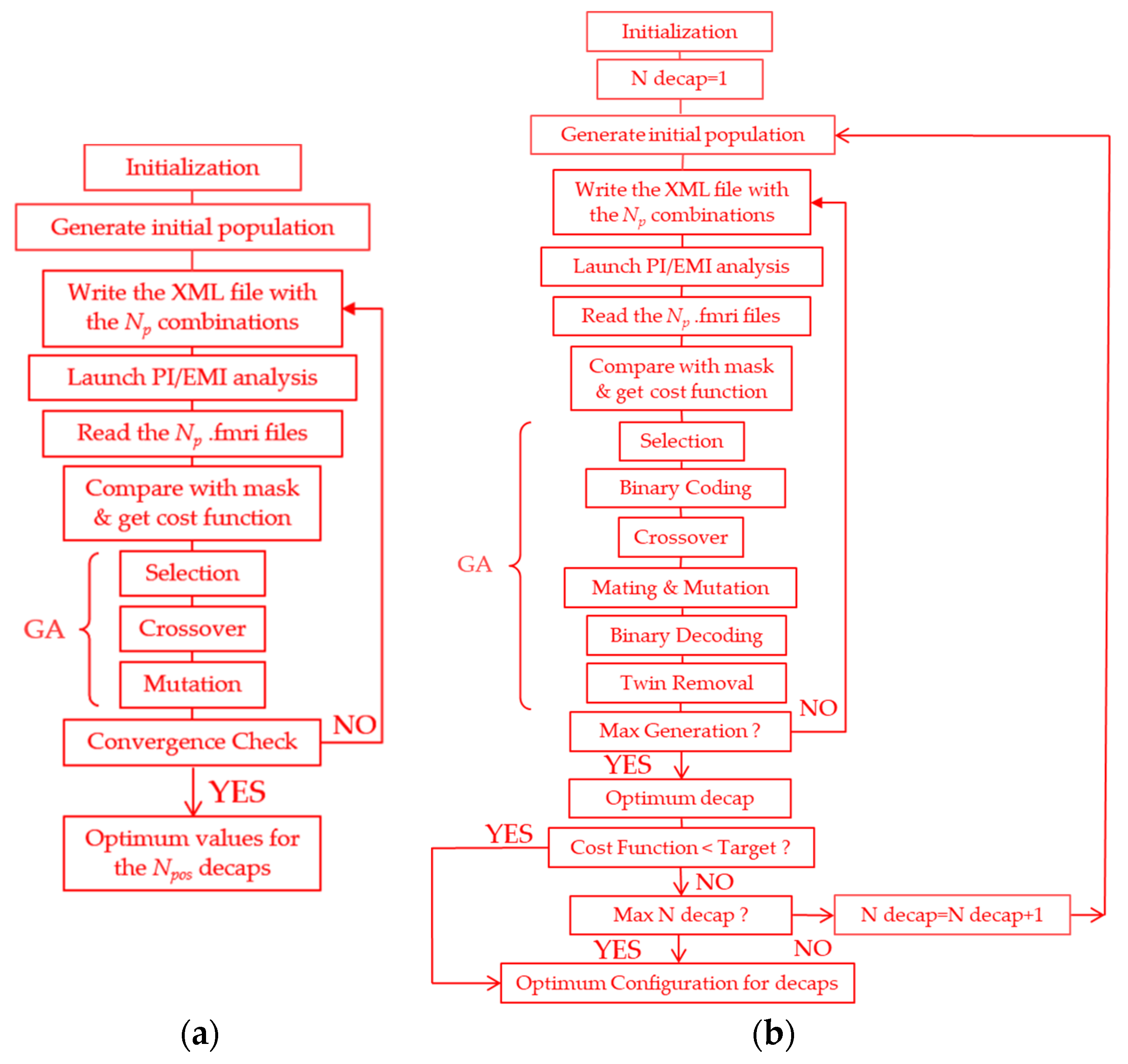
2. The Iterative Optimization Algorithm

2.1. Review of the Current GA Optimization

The general architecture of the genetic algorithm used in this work is the same as that used in Reference [14]. The GA allows a population, composed by Np chromosomes (chrom), to evolve according to specific laws toward a state able to minimize a cost function. The cost function fcost is a mathematical function whose input is each chromosome of the population, and the output is generally a value used for creating a rank among the Np chromosomes. In Reference [14] Equation (2), fcost was a function of the difference between the magnitude of the input impedance Zin evaluated in a single given position on the PDN and the magnitude of a specific impedance profile or mask, Zmask, that is defined by the PDN designer. In this work, fcost is different: It depends on the difference between the Zin evaluated in multiple positions (ports) on the PDN, and the same user-defined Zmask, as will be detailed later.
The high-level optimization flowchart of the initial GA is illustrated in Figure 1a. The GA is used in conjunction with a PI/EMI commercial PCB layout tool [34] (it is identified as ‘Design Force’ (DF) throughout the paper) that includes the simulation capability for the multilayer power distribution network design.
In Figure 1b, it is shown the flowchart of the improved GA, the object of this work, in which the new blocks of the binary coding/decoding, of the removal of the twin chromosomes, and of the iterative strategy are visible; they are discussed, in detail, in Section 2.2.

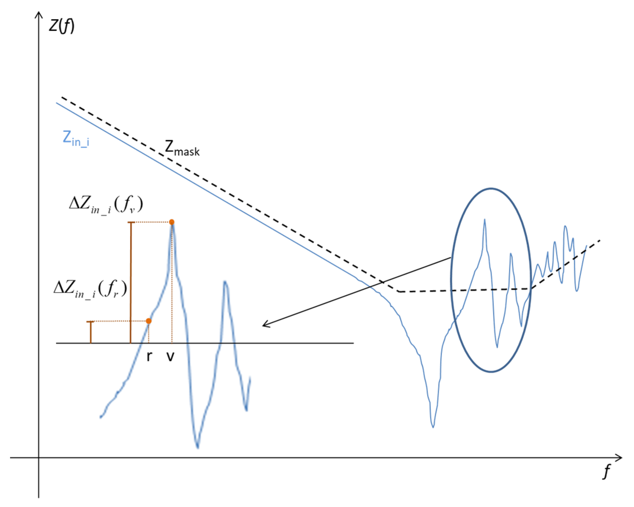
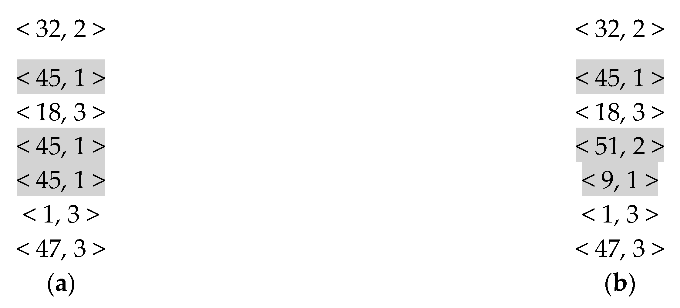
2.2. Iterative Approach based on an Improved Genetic Algorithm

Although the GA developed in Reference [14] gave acceptable results, there were margins of improvements aiming to a more robust and stable algorithm capable of dealing with more complex PDN designs. Therefore, some critical features have been modified or added.
The first of them was the change of fcost. The new fcost takes into consideration, simultaneously, the values of the frequency spectrum of the Zin computed at multiple ports, since this may be a more general case when the same PDN acts as power supply rail for multiple active devices. Alternatively, the use of a multiple-input impedance profiles may be required when a more rigorous design is necessary for a single large chip where, for example, the hundreds input power balls of the ball grid array (BGA) are spread on the IC footprint. In this work, the number of ports considered is Nports = 4. This extension of fcost to four (or in general Nports) ports allows the algorithm to choose the value and positioning of the decaps that minimize the input impedance only where is necessary, thus, improving the resilience of the PDN to the simultaneous switching noise (SSN) [8]. The new cost function is defined according to Equations (1)–(2):
f cos t = i = 1 N p o r t s f cos t _ i ,
f cos t _ i = j = 1 N f r e q Δ Z i n _ i ( f j ) N 1 ,
where fcost_i and ΔZin_i are the cost function and differential input impedance associated with the i-th port, respectively. Basically, given a frequency spectrum fj of a total of Nfreq points, N1 is the number of them, in which Zin_i(fj) is larger than a specific mask value Zmask(fj) at the same frequency, defined by the user. Zin_i is defined in Equation (3), and it is graphically illustrated in Figure 2. In this work, the number of ports considered is Nports = 4,
Δ Z i n _ i ( f j ) = { | Z i n _ i ( f j ) Z m a s k ( f j ) |   when   | Z i n _ i ( f j ) | | Z m a s k ( f j ) |   0   when   | Z i n _ i ( f j ) | < | Z m a s k ( f j ) | .
A further improvement of the original algorithm is accomplished in order to decrease its execution time when the handled decoupling problems become complex. To this aim, the GA, that is designed to be also implemented on programmable hardware, is directly based on a binary representation for the capacitor type and location, as shown in Figure 1b. All the genes into the chromosomes are represented as encoded binary strings with Ngene bits per gene. Quantization and encoding are performed according to the classic procedures used for the analog-to-digital conversion as in Reference ([35], Equation (2.5), (2.6)). It is worthy to mention that after encoding the current population, all the typical GA components, such as selection, crossover and mutation, are performed in the binary domain offering a higher randomness of configuration even using the random selected single point cross over for mating [29]. In the proposed algorithm, the decoding from binary to analog variables is only needed before computing the cost function, since the inputs to DF PI should be continuous variables. The decoding is implemented as in Reference ([35], Equation (2.7), (2.8)).
From the study carried out in Reference [14], it was evident that, due to the combination of the effects of the old cost function and the population size (the number of chromosomes at each generation) after mutation (the GA function that alters a given percentage of the bits in the list of chromosomes), a certain number of chromosomes were identical. This is a serious threat for the efficiency of the GA because limits its capability to explore the entire cost domain surface, and it can induce the convergence of the results toward a local minima. To avoid this trap, a twin removal routine introduced in References [32,33] has been introduced as a further improvement. Figure 3 shows the principle of the twin removal by considering, as an example, a population of Npop = 7 chromosomes. In particular, in each chromosome chrom = <gene1, gene2>, gene1 indicates the label of the position of the decaps (from 1 to 52) and gene2 represents the coded type (value) of the capacitor (from 1 to 3). Figure 3a shows an instance of the population after the last mutation during one of the GA iterations.
The presence of three identical chromosomes inhibits the algorithm to widely explore the cost domain surface and very likely it leads, at the next generation, more twins. The new algorithm removes the identical chromosomes in the populations keeping only the first one. The removed elements are substituted with newly random generated chromosomes. Such new chromosomes are also crosschecked for a further presence of unwanted twins. Figure 3b shows the population without twins now ready for computing the cost function.
In the previous implementation of the GA [14], given the total (or maximum) number of positions of the decaps Npos_max on the test PDN board that the designer intends to use, the optimal solution for Zin is found considering all the positions at once, generation after generation. This approach has shown to be correct, but very inefficient because, at each generation, it explores the cost function associated with all the possible Npos_max decap locations. The problem at hand lends itself to an iterative solution that at the n-th iteration takes advantages of the optimal solution at the previous (n-1)-th. In particular, the new algorithm starts looking at the optimal solution (in terms of decap position on the PDN board and their type) for one single capacitor. When the solution has been found, the algorithm looks at the solution (location and decap type) associated with a second capacitor. At the next iteration the optimal solution is sought for three decaps, but with two of them already fixed by the previous iterations. This loop is repeated up to up to Npos_max decaps, when the algorithm stops. At each iteration, at each increment of the number of decaps the GA looks at the optimal solution starting with an initial population that contains the last best choice. This iterative process is more efficient than the previous one in Reference [14] since the solution found involve inherently the minimum number of decaps. When the cost function reaches, or get lower than, the target value (it may be set to zero or to a particular value), the algorithm stops; the found solution is the one that employs the minimum decap number, and thus, it minimizes the component and manufacturing costs. Alternatively, the algorithm can be run until the placement of a maximum number of decap (Npos_max) is reached. Then the designer, by looking at the monotonically decreasing trend of the cost function, selects the number of decap to be applied to the PDN. This can be done, for instance, when the slope of the cost function reduces too much, thus, when adding more decaps has only a limited beneficial impact to the cost function.

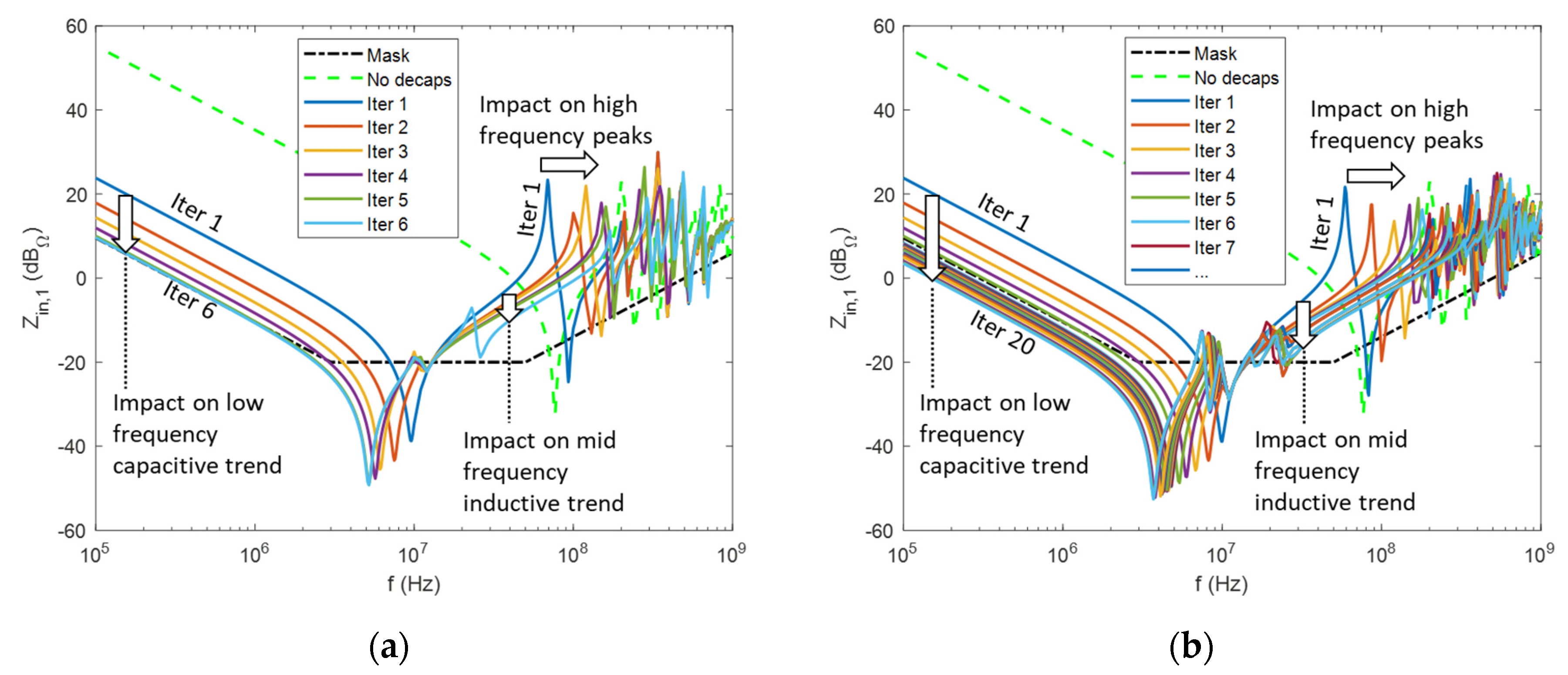
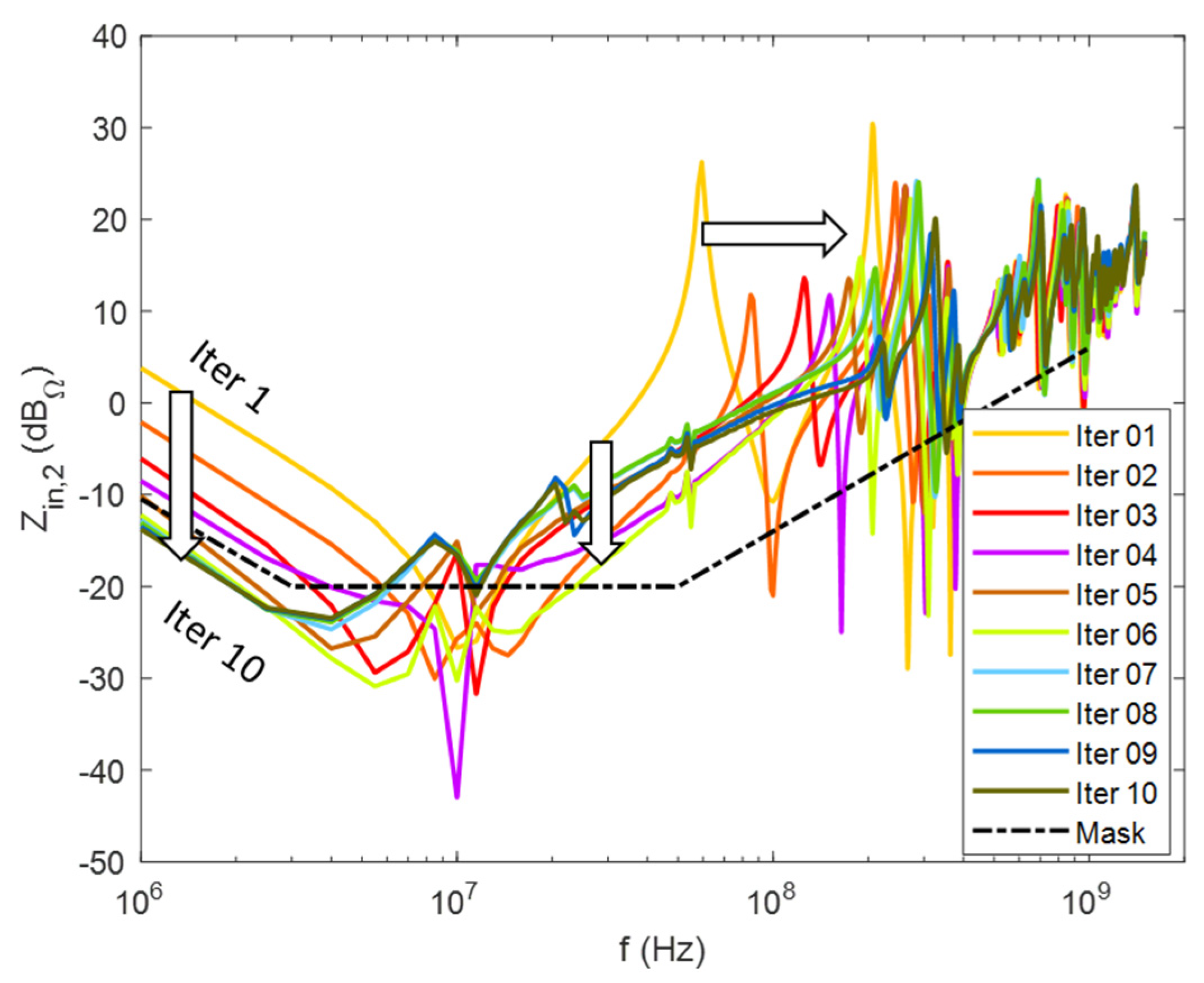
3. The PDN and Optimization Results

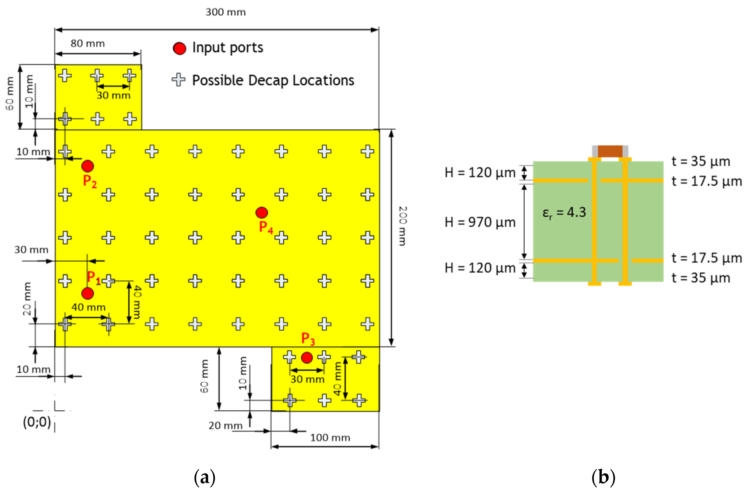
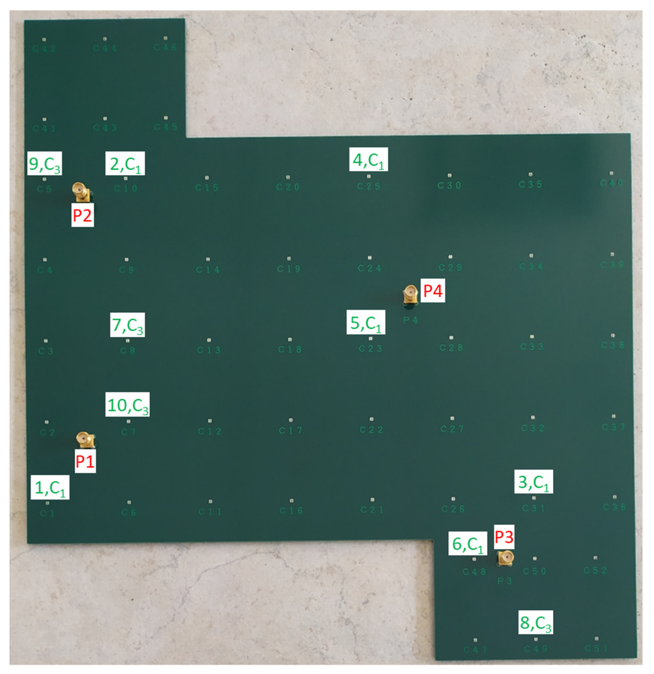
3.1. The PDN Structure

The test structure considered in this investigation, as shown in Figure 4, is similar to the one described in Reference [14] having the same planar dimensions. It is a four layer board built by 2 inner copper planes (electrical conductivity σCu = 5.7·× 108 S/m, thickness tcu = 0.0175 mm) representing a PDN with power (PWR) and ground (GND) nets; the places are separated by an FR4 dielectric (nominal relative dielectric permittivity εr = 4.3, nominal loss tangent tgδ = 0.02, thickness 0.97 mm).
The red circles represent the four input ports Pi from which the input impedance Zin is evaluated by the computational engine, since the generalized fcost considers simultaneously multiple Zin from different port locations. The cross symbol identifies all the possible locations where the decoupling capacitors (decaps) can be placed. The 52 total decap locations are spread uniformly all over the PCB surface with a distance among adjacent locations between 30mm and 40 mm. This strategy is of general use and suitable for an initial PDN design; once the decap placement is optimized, the location of each decap may be slightly adjusted according to other mechanical and routing constraints of the specific PCB design.
The present contribution targets a realistic scenario for the PDN optimization; thus, suitable values of capacitors are considered identified by C1, C2, C3, as summarized in Table 1. The three decoupling capacitors represent commercially available components [36]; their capacitance value, as well as the parasitic resistance and inductance, are different among them, thus, leading to different self-resonant frequencies. The use of such different components helps the wide band optimization, since smaller capacitance (to which usually corresponds a smaller parasitic inductance) is more effective at a higher frequency, and viceversa. These choices make the optimization more challenging, but, at the same time, the approach more realistic because, in the real world design of a PDN, usually the capacitors are selected by the on-the-shelf availability.
It is worth to note that the decaps selected for this study are characterized by a very low inductance, being specifically manufactured for power decoupling. The three capacitors are made by the same package, whose geometry and placement overview are reported in Figure 5. In particular, Figure 5b shows the layout of the decap pads and the vias for connection to the PWR and GND planes. The vias type and their location right at the pads are chosen for lowering the additional parasitic inductance that would be added to the decap equivalent straight inductance (ESL), thus, to minimize their impact on the overall decap effectiveness.

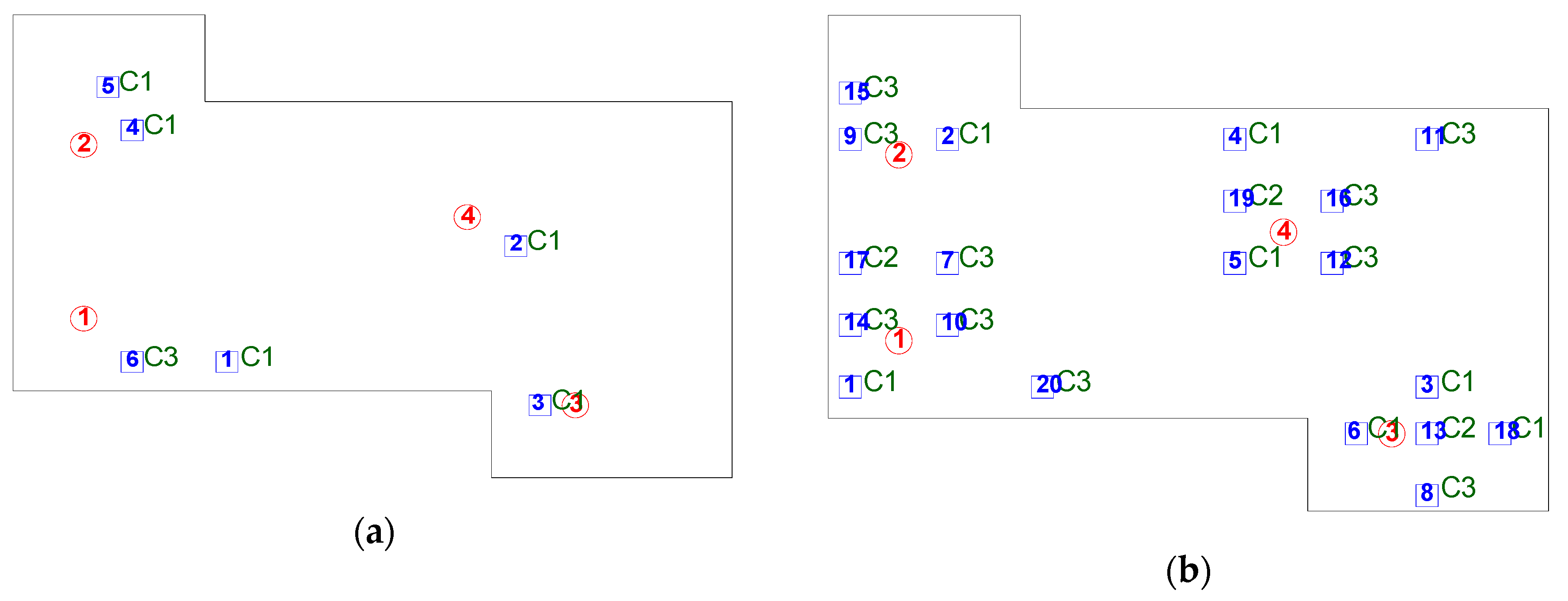
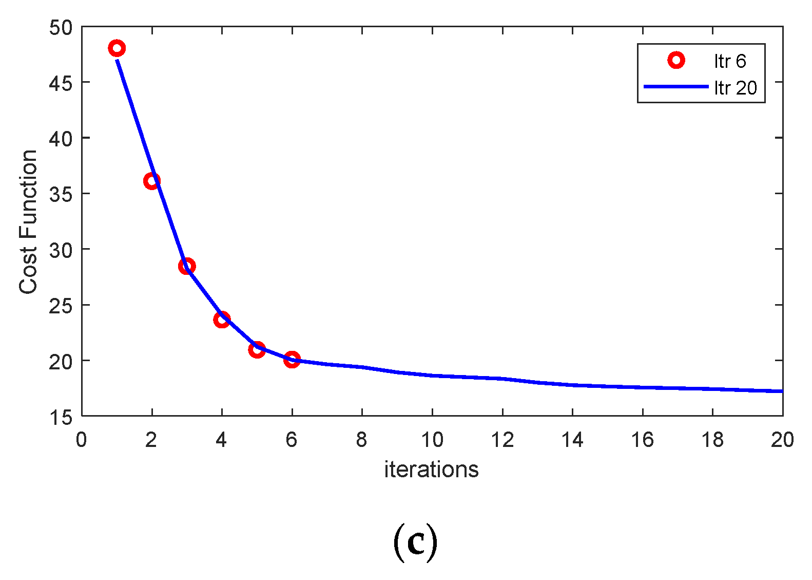
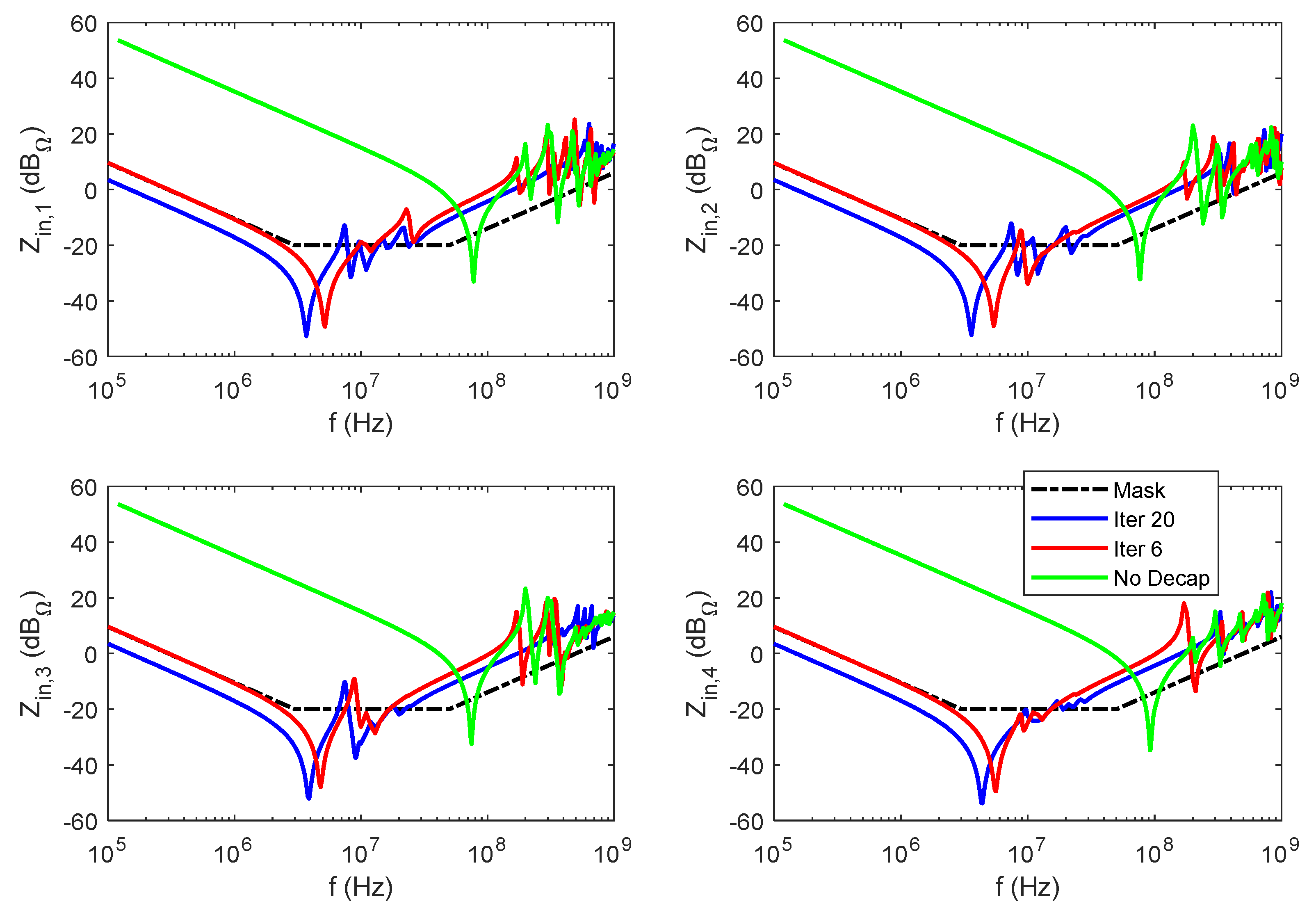
3.2. Optimization Results

The developed optimization algorithm is applied to the board defined in Figure four and whose input impedances at ports Pi are computed by DF PI. Two different optimization runs are launched based on different maximum iteration numbers; the first case is run for six iterations, thus, the GA-based algorithm runs, at most, six times, until six decaps are placed. The second case can reach up to 20 decaps, unless the cost function reaches zero.
The layout results are shown in Figure 6a for the case of six iterations and in Figure 6b for the case of 20 iterations. Specifically, the red circled numbers identify the location of the four ports; the squares represent the defined decap location, and the numbers inside identify the chronological order with which they have been placed by the GA, iteration after iteration, on the test PDN board. The Ci next to each square identifies the decap type according to Table 1. In both cases the cost function does not reach zero, thus, the optimization stops when the maximum iteration number is reached, as shown in Figure 6c. The trend of the two curves up to six iterations is very similar, although the randomness of the GA-based optimization provides a different layout for the first six decaps. Adding more capacitances makes the cost function still decreasing, but with a more gradual reduction. The initial steeper cost function trend mainly depends on the low frequency capacitive portion of the impedance; as soon as the impedance goes below the mask after the six decaps, the improvement given by any additional decap is reduced since the higher frequency impedance resonant peaks are only slightly decreased and moved to a higher frequency. This behavior is confirmed by the comparisons in Figure 7, where the four impedances are shown, and by the iterative evolution of the impedances at Port 1, shown in Figure 8.
One interesting consideration stemming from the above results is that, independently by the maximum number of available decaps for the optimization (also indicated as a number of iterations), the first positions on the PDN are always filled by C1 type. In particular, this occurs for the first 5 for the six iteration case and the first six for the 20 iteration case, as shown in Figure 6. This is a consequence of the optimization architecture for quickly bringing down the capacitive (or low frequency) portion of the frequency spectrum of the input impedance. As soon as this task is accomplished, the GA-based optimizer starts to place the other type of decaps (mainly the C3 type); they have less parasitic inductance, and thus, they are more effective at a higher frequency for moving the magnitude of the resonance peaks to lower values and to upper frequencies. Moreover, the resulting optimization offers a distribution of the decap close to the four ports, due to the shorter distance and, as a consequence, the corresponding lower “mounting” inductance associated with the loop between the integrated circuit (IC) power port and the decap. Although this distribution could be expected by the well-known impact of “local” decoupling strategies [16,22], the developed tool, together to the DF simulator, is able to obey to the physics of this problem, thus, relieving the designer from a trial-based PDN decoupling.
This demonstrates the effectiveness of the proposed iterative algorithm and its associated cost function definition for appropriately selecting the decap location and type according to the on-shelf availability.

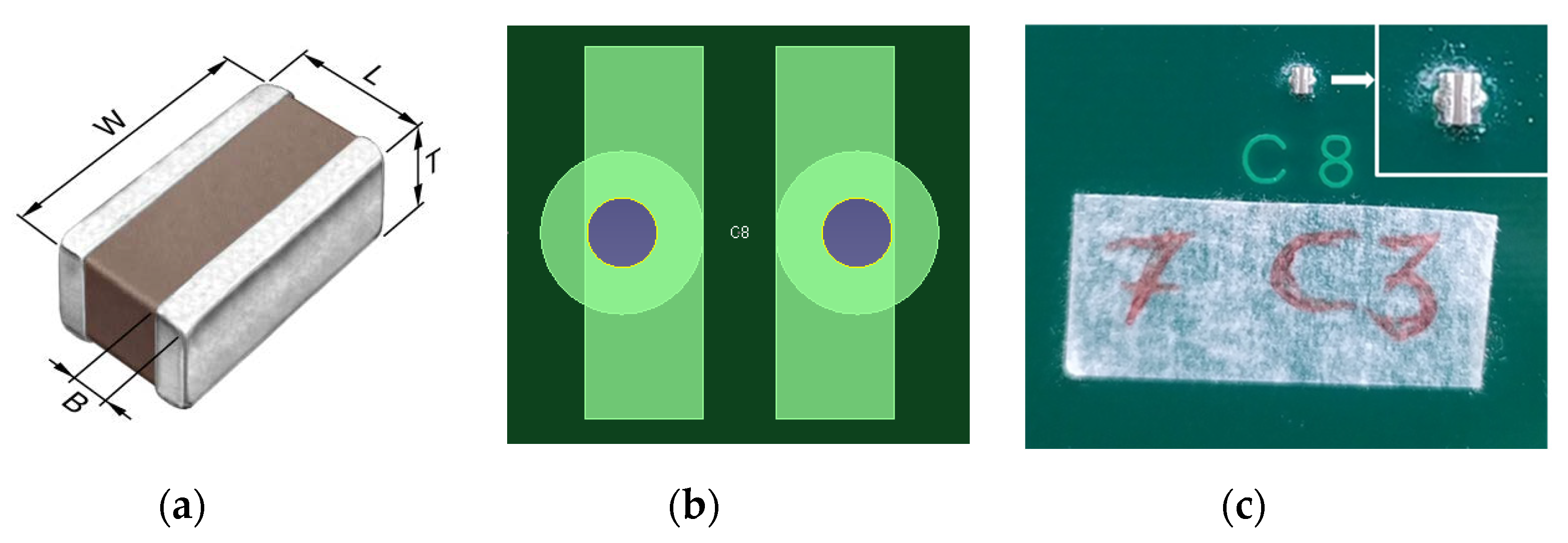
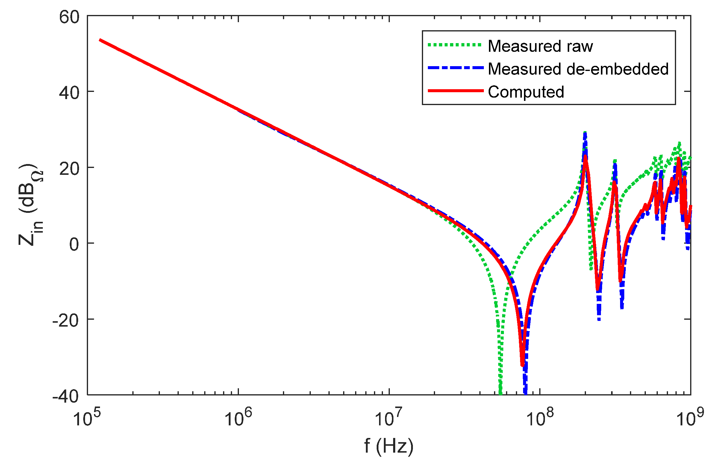
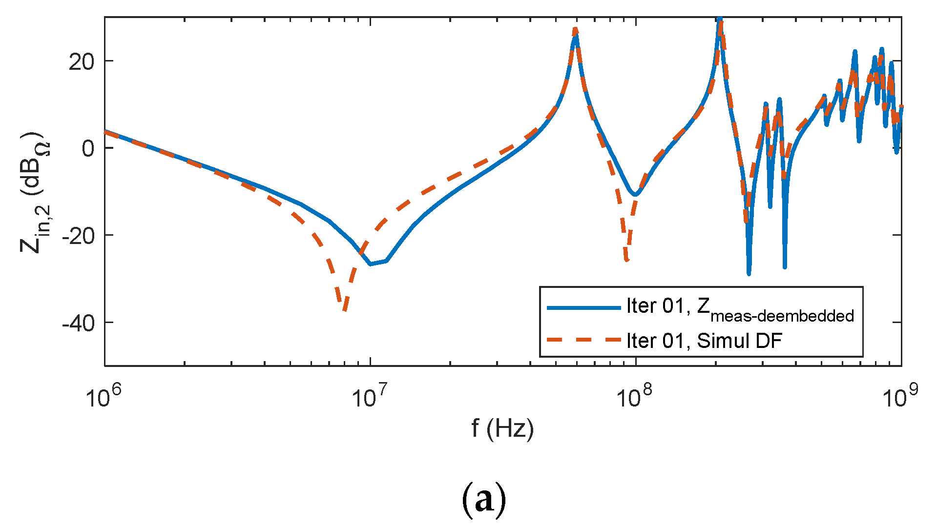
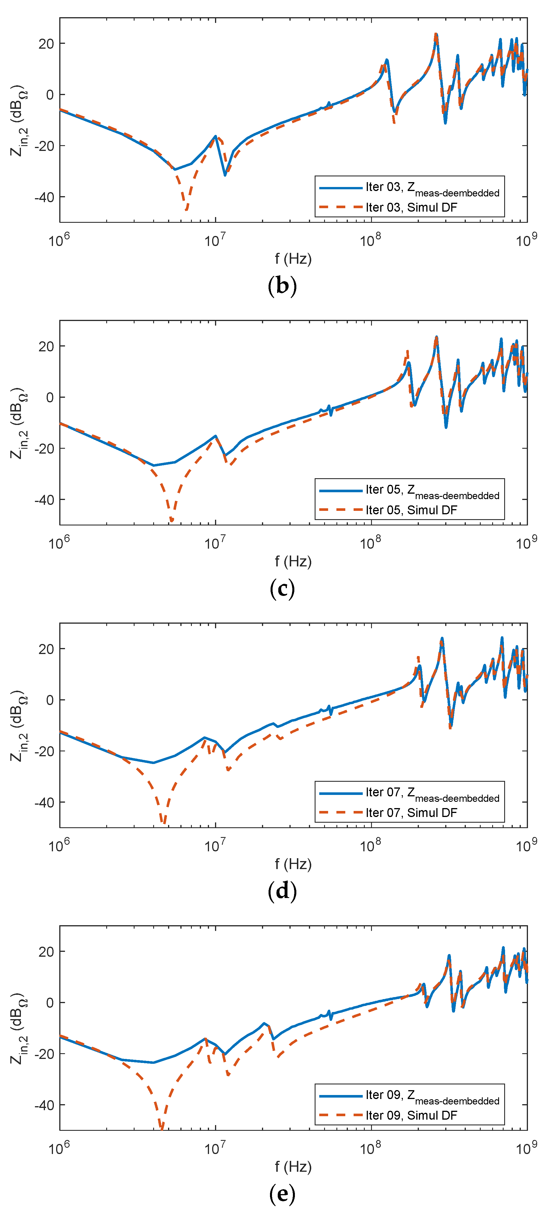
4. Experimental Validation

The proposed improved iterative GA optimization is validated by experimental measurements. As preliminary validation check, the input impedance at the left top port P2 of the PDN test board (see Figure 4a or Figure 11) without any decouplig capacitor (also indicated next as the “no decap” or “bare” board) has been measured by a Vector Network Analyzer (VNA) and computed by DF PI. A relevant aspect to be taken into account when performing such measurement, is the impact of the SMA connector that cannot be taken into account by the simulator. Although the board layout considers the SMA vias, the portion of the SMA connector above the board surface needs to be de-embedded for an accurate comparison. The calibration of the VNA is performed using the standard SOLT coaxial kit, and it sets the calibration reference at the cable ends. Therefore, an additional inductive (LSMA) contribution is given by the SMA connector between the cable and the board surface, as sketched in Figure 9a.
The evaluation of LSMA is carried out by measuring the single SMA connector after removing its pins and electrically shorting the four GND contacts to the PWR (central) contact, as shown in Figure 9b. The measured scattering parameter S11 is converted to its corresponding impedance parameter, and then the inductance is extracted, as reported in Figure 9c. The inductance values at low frequency may be affected by the measurement error, due to the reduced VNA sensitivity when performing phase measurements at low frequency. Above 40 MHz the impedance profile is quite flat and stable: It allows to extract an equivalent value LSMA = 1.78 nH, as identified by the horizontal line in the figure.
Once known its value, the LSMA inductance is de-embedded from the measured input impedance at port P2 using the Keysight ADS circuit simulator [37], now allowing a meaningful comparison between measured and simulated results. The comparison between the measured and simulated input impedances are shown in Figure 10. The impact of LSMA is evident from the measured curves; the de-embedding of LSMA leads to a good agreement between the measured and simulated impedances. According to the IEEE Standard P1597 [38], the Feature Selective Validation technique [39,40] is used to quantify the matching of the two curves in Figure 3. The matching is classified as “excellent” [38] being the FSV figure of merits GRADE = 1 and SPREAD = 1.
The decap positions and values in Figure 6b obtained after the optimization based on the 20 iterations are reproduced on the manufactured board. The board PDN with the four ports (P1 to P4) – each one with its SMA connectors mounted-and 10 of the 20 decoupling capacitors soldered are shown in Figure 11. The labels next to each decap identify the iteration number (from 1 to 10) at which each decap has been placed by the GA, and the capacitor type (C1, C2, or C3) assigned to it. In the experimental tests, the first 10 decaps are mounted, and the input impedances at the four ports are measured after the placement of each new capacitor. All impedance curves at port P2 are reported in Figure 12. The impedance trend when adding more and more decaps is similar to the one from simulations, shown in Figure 8. Further validation is given by comparing some sample curves from measured and simulated data. The measured input impedances are de-embedded according to the procedure described above and, for the cases of 1, 3, 5, 7, and 9 decaps, they are compared to the corresponding impedances evaluated by DF PI. The results are shown in Figure 13. It is worthy to note that the number of frequency points of the measured data is smaller and based on a linear scale, compared to the larger number of points based on a logarithmic scale generated by the simulation tool. This difference leads to a lack of resolution of the measured curves around the first resonance notch at around 80 MHz. Nevertheless, a good agreement is found, especially when C1 type of decap is added, as for the cases of 1, 3, and 5 decaps, shown in Figure 13a–c. Some discrepancies between measured and simulated results occur in the intermediate frequency range when the C3 type of decap (lowest value) is added, at iteration 7 and 9, as from Figure 13d,e. This not perfect matching is due to the inherent small difference between the nominal values, used in the simulations, of the ESL of capacitors type C3 and the corresponding values of the actually-mounted components.

5. Conclusions

An efficient procedure is developed for the optimum placement of decoupling capacitors for the PDN design at PCB level. The procedure is based on an improved GA modified with respect to the previously developed version. The new optimization is based on an iterative approach, thus, the GA identifies the best location for each new single decap that needs to be placed. The developed algorithm is of general use; thus, no restrictions are set in terms of target impedance to be used as a reference. The effectiveness of the developed optimization is confirmed by the simulated test cases, for which the cost function always decreases at each iteration, and for which the decaps are accordingly placed around the input ports achieving an effective minimization of the parasitic mounting inductance. The simulated cases are carefully tested experimentally on the corresponding manufactured test board. The good agreement between measured and simulated input impedances, and the trend of the measured impedances at each iteration, confirm the validity of the proposed optimization approach. The next step, whose conceptualization is already in an advanced phase, of this research project, aims to exploit machine learning (ML) algorithms for performance improvement of the optimization process. In particular, more engineering-wise initial configurations for the decaps (i.e., their as close as a possible connection to the IC power ports or pins, their parallel connection) are learned by the algorithms and then presented to the optimizer. The results are ranked and dynamically added to the knowledge (or training set) of the ML algorithms.

Author Contributions

Conceptualization, A.O., and M.B.; methodology, A.O. and F.d.P.; software, S.P., C.O., R.C. and M.B.; validation, F.d.P. and C.O.; writing—original draft preparation, A.O. and F.d.P.; writing—review and editing, A.O. and F.d.P.

Funding

This research was funded by Google, 2017 Google Faculty Research Award.

Acknowledgments

The authors would like to thank Zhiping Yang at Google for his valuable support, the useful discussions and the insightful comments for the development of this work and ZUKEN GmbH for having supported the project with its software.

Conflicts of Interest

The authors declare no conflict of interest.

References

  1. Armstrong, C. Debug and analysis considerations for optimizing signal integrity in your internet of things design. In Proceedings of the IEEE International Symposium on Electromagnetic Compatibility & Signal/Power Integrity (EMCSI), Washington, DC, USA, 7–11 August 2017; pp. 20–24. [Google Scholar]
  2. Nadal, J.; Nour, C.A.; Baghdadi, A. Flexible and efficient hardware platform and architectures for waveform design and proof-of-concept in the context of 5G. AEU Int. J. Electron. Commun. 2018, 97, 85–93. [Google Scholar] [CrossRef]
  3. Bhoyar, P.; Dhok, S.; Deshmukh, R. Hardware implementation of secure and lightweight Simeck32/64 cipher for IEEE 802.15.4 transceiver. AEU Int. J. Electron. Commun. 2018, 90, 147–154. [Google Scholar] [CrossRef]
  4. Swaminathan, M.; Han, K.J. Design and Modeling for 3D ICs and Interposers; World Sci.: Singapore, 2014. [Google Scholar]
  5. Archambeault, B.R. PCB Design for Real-World EMI Control; Springer Science and Business Media LLC: New York, NY, USA, 2002. [Google Scholar]
  6. Hall, S.H.; Heck, H.L. Advanced Signal Integrity for High-Speed Digital Designs; Wiley: Hoboken, NJ, USA, 2009. [Google Scholar]
  7. Wiklundh, K.; Stenumgaard, P. EMC challenges for the internet of things. In Proceedings of the International Symposium on Electromagnetic Compatibility EMC EUROPE, Angers, France, 4–7 September 2017; pp. 1–6. [Google Scholar]
  8. Smith, L.D.; Bogatin, E. Principles of Power Integrity for PDN Design; Prentice-Hall: New York, NY, USA, 2016. [Google Scholar]
  9. Zamek, I.; Boyle, P.; Li, Z.; Sun, S.; Chen, X.; Chandra, S.; Li, T. Modeling FPGA current waveform and spectrum and PDN noise estimation. In Proceedings of the DesignCon, Santa Clara, CA, USA, 4–7 February 2008. [Google Scholar]
  10. Orlandi, A.; Archambeault, B.; de Paulis, F.; Connor, S. Electromagnetic Bandgap (EBG) Structures: Common Mode Filters for High Speed Digital Systems; IEEE Press/Wiley: New York, NY, USA, 2017. [Google Scholar]
  11. Wu, T.; Chuang, H.; Wang, T. Overview of Power Integrity Solutions on Package and PCB: Decoupling and EBG Isolation. IEEE Trans. Electromagn. Compat. 2010, 52, 346–356. [Google Scholar] [CrossRef]
  12. Yang, S.; Cao, Y.S.; Ma, H.; Cho, J.; Ruehli, A.E.; Drewniak, J.L.; Li, E. PCB PDN Prelayout Library for Top-Layer Inductance and the Equivalent Model for Decoupling Capacitors. IEEE Trans. Electromagn. Compat. 2018, 60, 1898–1906. [Google Scholar] [CrossRef]
  13. Zhang, L.; Zhang, Z.; Huang, C.; Deng, H.; Lin, H.; Tseng, B.-C.; Drewniak, J.; Hwang, C. Decoupling Capacitor Selection Algorithm for PDN Based on Deep Reinforcement Learning. In Proceedings of the IEEE International Symposium on Electromagnetic Compatibility, Signal & Power Integrity (EMC+SIPI), New Orleans, LA, USA, 22–26 July 2019; Institute of Electrical and Electronics Engineers (IEEE): Piscataway, NJ, USA, 2019; pp. 616–620. [Google Scholar]
  14. Piersanti, S.; Cecchetti, R.; Olivieri, C.; De Paulis, F.; Orlandi, A.; Buecker, M. Decoupling Capacitors Placement at Board Level Adopting a Nature-Inspired Algorithm. Electronics 2019, 8, 737. [Google Scholar] [CrossRef]
  15. Barnes, H.; Sandler, S. Decoupling Capacitor Optimization for Flat Z PCB Power Distribution Networks. In Proceedings of the IEEE Symposium on Electromagnetic Compatibility, Signal Integrity and Power Integrity (EMC, SI & PI), Long Beach, CA, USA, 30 July–3 August 2018; p. 1. [Google Scholar]
  16. Shringarpure, K.; Zhao, B.; Wei, L.; Archambeault, B.; Ruehli, A.; Cracraft, M.; Cocchini, M.; Wheeler, E.; Fan, J.; Drewniak, J. On finding the optimal number of decoupling capacitors by minimizing the equivalent inductance of the PCB PDN. In Proceedings of the IEEE International Symposium on Electromagnetic Compatibility (EMC), Raleigh, NC, USA, 4–8 August 2014; pp. 218–223. [Google Scholar]
  17. Erdin, I.; Achar, R. Multipin Optimization Method for Placement of Decoupling Capacitors Using a Genetic Algorithm. IEEE Trans. Electromagn. Compat. 2018, 60, 1662–1669. [Google Scholar] [CrossRef]
  18. Kadlec, P.; Marek, M.; Štumpf, M.; Šeděnka, V. PCB Decoupling Optimization with Variable Number of Capacitors. IEEE Trans. Electromagn. Compat. 2018, 1–8. [Google Scholar] [CrossRef]
  19. Su, H.; Sapatnekar, S.S.; Nassif, S.R. Optimal decoupling capacitor sizing and placement for standard-cell layout designs. IEEE Trans. Comput. Aided Des. Integr. Circuits Syst. 2003, 22, 428–436. [Google Scholar] [CrossRef]
  20. Wang, X.; Cai, Y.; Zhou, Q.; Tan, S.X.D.; Eguia, T. Decoupling capacitance efficient placement for reducing transient power supply noise. In Proceedings of the IEEE/ACM International Conference on Computer—Aided Design—Digest of Technical Papers, San Jose, CA, USA, 2–5 November 2009; pp. 745–751. [Google Scholar]
  21. Han, G. Simple and fast method of on-board decoupling capacitor selection and placement. In Proceedings of the IEEE Electrical Design of Advanced Packaging and Systems Symposium (EDAPS), Haining, China, 14–16 December 2017; Institute of Electrical and Electronics Engineers (IEEE): Piscataway, NJ, USA, 2017; pp. 1–3. [Google Scholar]
  22. Piersanti, S.; de Paulis, F.; Olivieri, C.; Orlandi, A. Decoupling Capacitors Placement for a Multichip PDN by a Nature-Inspired Algorithm. IEEE Trans. Electromagn. Compat. 2018, 60, 1678–1685. [Google Scholar] [CrossRef]
  23. Kim, J.; Wu, S.; Wang, H.; Takita, Y.; Takeuchi, H.; Araki, K.; Feng, G.; Fan, J. Improved target impedance and IC transient current measurement for power distribution network design. In Proceedings of the IEEE International Symposium on Electromagnetic Compatibility, Fort Lauderdale, FL, USA, 25–30 July 2010; pp. 445–450. [Google Scholar]
  24. Sun, Y.; Kim, J.; Hwang, C. Jitter-Aware Target Impedance. In Proceedings of the IEEE International Symposium on Electromagnetic Compatibility, Signal & Power Integrity (EMC+SIPI), New Orleans, LA, USA, 22–26 July 2019; pp. 217–222. [Google Scholar]
  25. Xu, J.; Bai, S.; Nalla, K.; Sapozhnikov, M.; Drewniak, J.L.; Hwang, C.; Fan, J. Power Delivery Network Optimization Approach using an Innovative Hybrid Target Impedance. In Proceedings of the IEEE International Symposium on Electromagnetic Compatibility, Signal & Power Integrity (EMC+SIPI), New Orleans, LA, USA, 22–26 July 2019; Institute of Electrical and Electronics Engineers (IEEE): Piscataway, NJ, USA, 2019; pp. 211–216. [Google Scholar]
  26. Patnaik, S.; Yang, X.; Nakamatsu, K. Nature-Inspired Computing and Optimization; Springer: Zurich, Switzerland, 2016. [Google Scholar]
  27. Koziel, S.; Leifsson, L.; Yang, X. Simulation-Driven Modeling and Optimization; Springer: Zurich, Switzerland, 2016. [Google Scholar]
  28. Günel, T.; Aydemir, M.E. Application of Continuous Parameter Genetic Algorithm to the Problem of Synthesizing Bandpass Distributed Amplifiers. AEU Int. J. Electron. Commun. 2002, 56, 351–354. [Google Scholar] [CrossRef]
  29. Haupt, R.L.; Werner, D.H. Genetic Algorithms in Electromagnetics; Wiley: Hoboken, NJ, USA, 2007. [Google Scholar]
  30. Mostafa, S.S.; Horta, N.; Ravelo-García, A.G.; Morgado-Dias, F. Analog active filter design using a multi objective genetic algorithm. AEU Int. J. Electron. Commun. 2018, 93, 83–94. [Google Scholar] [CrossRef]
  31. Kaya, T.; Guler, H. A hybrid genetic algorithm for analog active filter component selection. AEU Int. J. Electron. Commun. 2018, 86, 1–7. [Google Scholar] [CrossRef]
  32. Imani, M.; Pakizeh, E.; Saraee, M. Improving Genetic Algorithm with the Help of Novel Twin Removal Method. In Proceedings of the Tenth IASTED International Conference on Artificial Intelligence and Applications, Innsbruck, Austria, 15–17 February 2010; pp. 16–21. [Google Scholar]
  33. Hoque, M.T.; Chetty, M.; Dooley, L.S. Generalized Schemata Theorem Incorporating Twin Removal for Protein Structure Prediction. In Computer Vision–ECCV 2012; Springer Science and Business Media LLC: New York, NY, USA, 2007; pp. 84–97. [Google Scholar] [Green Version]
  34. Zuken, Design Force User Manual. Available online: https://www.zuken.com/it/products/pcb-design/cr-8000/products/design-force 69 (accessed on 2 September 2019).
  35. Haupt, R.L.; Haupt, S.E. Practical Genetic Algorithms, 2nd ed.; Wiley: New York, NY, USA, 2004. [Google Scholar]
  36. TDK. Available online: https://product.tdk.com/en/search/capacitor/ceramic/mlcc/characteristic/ (accessed on 4 February 2019).
  37. Advanced Design System (ADS). Available online: www.keysight.com/en/pc-1297113/advanced-design-system-ads (accessed on 2 November 2018).
  38. IEEE Standard P1597. Standard for Validation of Computational Electromagnetics Computer Modeling and Simulation—Part 1; IEEE: Piscataway, NY, USA, February 2008. [Google Scholar]
  39. Duffy, A.; Martin, A.; Orlandi, A.; Antonini, G.; Benson, T.; Woolfson, M. Feature Selective Validation (FSV) for Validation of Computational Electromagnetics (CEM). Part I—The FSV Method. IEEE Trans. Electromagn. Compat. 2006, 48, 449–459. [Google Scholar] [CrossRef]
  40. Orlandi, A.; Duffy, A.; Archambeault, B.; Antonini, G.; Coleby, D.; Connor, S.; Duffy, A. Feature Selective Validation (FSV) for Validation of Computational Electromagnetics (CEM). Part II—Assessment of FSV Performance. IEEE Trans. Electromagn. Compat. 2006, 48, 460–467. [Google Scholar] [CrossRef]
Figure 1. High-level genetic algorithm (GA) optimization flow: (a) Algorithm from Reference [14] and (b) the proposed improved iterative algorithm.
Electronics 08 01219 g001
Figure 2. Graphical interpretation of Equation (3).
Electronics 08 01219 g002
Figure 3. Population: (a) With twins and (b) after twin removal.
Electronics 08 01219 g003
Figure 4. (a) The test power delivery network (PDN) boards and (b) its stack-up.
Electronics 08 01219 g004
Figure 5. (a) Overview of the decap package with nominal dimensions B = 0.1 mm, T = 0.5 mm, W = 1.6 mm, L = 0.8 mm. (b) Layout for the decap with the pad on the top layer and the vias; (c) Placement of decap at location C8; the decap type C3 is placed at the 7th iteration.
Electronics 08 01219 g005
Figure 6. Optimal placement and design of decoupling capacitors for (a) 6 and (b) 20 iterations (number of decaps); (c) comparison between the cost functions for 6 and 20 iterations.
Electronics 08 01219 g006aElectronics 08 01219 g006b
Figure 7. Frequency spectra of the optimized input impedances at the four ports for six and 20 iterations (number of decaps). The input impedances are compared to the case of the PDN with no decaps and to the user-defined mask.
Electronics 08 01219 g007
Figure 8. Iterative evolution of the input impedances at Port P1 for the case of (a) maximum six iterations, and (b) maximum 20 iterations (number of decaps).
Electronics 08 01219 g008
Figure 9. (a) Identification of the LSMA additional inductance; (b) measurement setup to extract LSMA; (c) measured LSMA.
Electronics 08 01219 g009
Figure 10. Comparison between measured and simulated input impedance at Port 2 for the case of the bare board.
Electronics 08 01219 g010
Figure 11. Manufactured board with mounted SMA connectors at the ports and decoupling capacitors.
Electronics 08 01219 g011
Figure 12. Measured input impedances (after de-embedding) at port P2 for iteration 1 (1 mounted decap) to iteration 10 (10 mounted decaps).
Electronics 08 01219 g012
Figure 13. Comparisons between measured and simulated impedances at port P2 for different numbers of mounted capacitors—(a) 1 C1, (b) 3 C1, (c) 5 C1, (d) 6 C1 plus 1 C3 and (e) 6 C1 plus 3 C3.
Electronics 08 01219 g013aElectronics 08 01219 g013b
Table 1. Electrical properties of the three TDK Multilayer Ceramic Chip decoupling capacitors (C1, C2, C3).
ParameterProduct NumberC (nF)ESL (pH)ESR (m)
C1C0510X5R1C104M030AC1002228.9
C2C0816X5R1C473M050AC4715421.4
C3C0816X5R1C223M050AC2214225.2

