A Parallel Connected Component Labeling Architecture for Heterogeneous Systems-on-Chip


1
Department of Mechanical, Energy and Management Engineering, University of Calabria, 87036 Arcavacata di Rende, Italy
2
Department of Informatics, Modeling, Electronics and System Engineering, University of Calabria, 87036 Arcavacata di Rende, Italy
*
Author to whom correspondence should be addressed.
Electronics 2020, 9(2), 292; https://doi.org/10.3390/electronics9020292
Submission received: 20 December 2019
/
Revised: 4 February 2020
/
Accepted: 6 February 2020
/
Published: 8 February 2020
(This article belongs to the Special Issue Recent Advances in Field-Programmable Logic and Applications)
Abstract
:Connected component labeling is one of the most important processes for image analysis, image understanding, pattern recognition, and computer vision. It performs inherently sequential operations to scan a binary input image and to assign a unique label to all pixels of each object. This paper presents a novel hardware-oriented labeling approach able to process input pixels in parallel, thus speeding up the labeling task with respect to state-of-the-art competitors. For purposes of comparison with existing designs, several hardware implementations are characterized for different image sizes and realization platforms. The obtained results demonstrate that frame rates and resource efficiency significantly higher than existing counterparts are achieved. The proposed hardware architecture is purposely designed to comply with the fourth generation of the advanced extensible interface (AXI4) protocol and to store intermediate and final outputs within an off-chip memory. Therefore, it can be directly integrated as a custom accelerator in virtually any modern heterogeneous embedded system-on-chip (SoC). As an example, when integrated within the Xilinx Zynq-7000 X C7Z020 SoC, the novel design processes more than 1.9 pixels per clock cycle, thus furnishing more than 30 2k × 2k labeled frames per second by using 3688 Look-Up Tables (LUTs), 1415 Flip Flops (FFs), and 10 kb of on-chip memory.
1. Introduction
Machine vision, image processing, and pattern recognition algorithms often require segmented visual objects and/or regions of interest to be identified and analyzed. To this aim, the well-known connected component labeling (CCL) and connected component analysis (CCA) operations are typically performed [1,2]. While the main goal of CCL is to assign a unique label to all pixels belonging to the same connected component in a binary input image, the objective of CCA is to extract, for each recognized connected component, features, such as area, perimeter, bounding box, center of gravity, etc.
The CCL and CCA algorithms are intermediate steps of more complex tasks [3,4]. Therefore, executing them as fast and efficiently as possible is crucial to avoid bottleneck in the overall workload [2,5,6,7,8,9,10,11,12,13,14,15,16,17,18,19,20,21,22,23,24,25,26,27,28,29,30,31].
While, in some applications, only synthetic features are required for the subsequent image analysis [1,5], in many others, fully labeled output images are needed [3]. In the former, the feature extraction step is fused with the labeling one, thus simplifying the whole process. In the latter, these simplifications are not possible, and the processing time becomes much higher. This research work is specifically focused on the design of custom hardware architectures for the acceleration of the CCL computation. Since the connected components can have complex shapes and connectivity, it represents a very time-consuming basic operation to perform on digital images [2]. CCL algorithms are classified into several categories [2], based on how many raster scans of the input image are required to provide the output labeled image. The latter has the same size of the input image and contains the labels assigned to the input pixels.
Several attempts to improve the performance of these algorithms were presented in the recent past. They exploit parallelism by means of either multi-core processors and Graphics Processing Units (GPUs) [5,27,28,29,30,31] or custom hardware architectures [10,11,14,15,16,17,18,19,20,21,22,23,26]. As it is well known, for many consumer applications, like those related to the Internet of things (IoT), reaching high speed is as important as achieving low cost and high energy efficiency [16,32]. The design discussed in this paper is tailored to such a class of applications. Therefore, heterogeneous FPGA-based systems-on-chip (SoCs) were chosen as the target realization platforms. These systems merge the flexibility offered by operating systems and by software routines, typically needed to control peripheral interfaces and interconnection resources, with the computational capability of highly parallel specialized hardware architectures that may provide the desired acceleration.
This paper presents a novel two-scan hardware-oriented labeling approach able to parallelize the CCL process at both pixel and frame level. In order to do this, it exchanges data with an external memory. The proposed architecture elaborates two input binary pixels in parallel and provides two labeled pixels at once. Furthermore, while the generic input binary image undergoes its first raster scan for being provisionally labeled, the previously elaborated frame is scanned for the final step, and its output is transferred to the appropriate destination, thus maximizing the achievable throughput. Both input and output data bandwidths are kept limited and both read and write accesses on the image memory are maintained regularly. The proposed design complies with the fourth generation of the high-performance advanced extensible interface (AXI4) protocol [33], and, differently from several existing hardware accelerators designed as standalone modules [23,29,30,31], time and resource overheads required to comply with the communication protocol are taken into account.
For purposes of comparison with existing competitors, different implementation platforms were used. Speed performances and resources requirements of the novel parallel hardware design were analyzed for image sizes ranging from 640 × 480 to 2k × 2k with the number of manageable labels varying between 64 and 8192. Obtained results demonstrate that the proposed parallel CCL architecture can process at least 1.88 pixels per clock cycle, which is a throughput that none of the existing counterparts reaches. This advantage is obtained with an on-chip memory requirement ranging from 0.375 to 104 kb, which is significantly lower than the referred competitors. As an example, when integrated within a complete heterogeneous embedded SoC realized using the Xilinx Zynq-7000 X C7Z020 device, the implementation able to process 2k × 2k binary images with at most 1024 labels sustains the 30.3 fps frame rate by occupying only 3688 LUTs, 1414 FFs, and 10 kb of on-chip Random Access Memory (RAM). When compared to the most efficient competitor [22], at a parity of image size and number of managed labels, the proposed design exhibits a resources efficiency ~4.7 times higher.
The rest of the paper is organized as follows: a brief background on CCA and CCL is provided in Section 2; the novel CCL approach is introduced in Section 3; Section 4 describes the parallel hardware architecture purpose-designed to integrate the proposed CCL method within a complete embedded SoC; implementation and comparison results are provided in Section 5; finally, conclusions are drawn in Section 6.
2. Background and Related Works
CCA and CCL play a crucial role in many image analysis and pattern-recognition tasks. The main goal of the CCA is to extract, for the connected components (i.e., different objects) in an input image, some features that are subsequently processed depending on the specific application. One-scan CCA algorithms [1,2,6,9,10,15,17,21,24,26] are particularly efficient since they exploit a provisional CCL step to distinguish the different connected components in the input image. The latter is scanned in raster order, and each foreground pixel is labeled depending on its four or eight neighbors, thus leading to a four-connected or an eight-connected neighborhood, respectively. The critical event, called label collision or equivalence, happens when the pixels in the neighborhood have different labels. The ambiguity occurring in this case is typically solved by assigning to the current pixel the lowest equivalent label. Due to the even more complicated condition that intertwines multiple collisions within a chain of equivalences, resolving the chains of collisions efficiently is very difficult [2]. Even though the provisional CCL could not assign unique labels to the pixels belonging to the same connected components, it allows extracting the desired features correctly, without performing further image scans.
However, several applications strictly require the complete correct labeled image [3,15]. In these cases, to ensure that all the pixels of the generic connected component are uniquely labeled, at least one further image scan is necessary to assign the final unambiguous label to each pixel of the input image. Based on how many raster scans are performed overall to provide the final labeled image, the CCL approaches known in literature can be classified into three main categories: one scan, two scan, and multi-scan [2].
The one-scan CCL architecture recently presented in Reference [15] exploits a run-length encoding technique and reaches the noticeable speed performance of ~ 39 2k × 1.5k frames per second, at the running frequency of 300 MHz. However, it shows a relatively low throughput rate of ~ 3.73 clock cycles per pixel and requires ~ 2.5 Mb of on-chip memory, generally available only in expensive high-end devices.
The two-scan algorithms require only two regular forward scans to provide completely labeled images. During the first scan, the provisionally labeled image is produced and encountered collisions are recorded. Then, the collision resolution step is performed. Finally, through the second raster scan, foreground pixels receive their final labels depending on the information recorded during the previous scan. The two-scan approaches allow achieving a good trade-off between speed performances and resources requirements, thus making their hardware designs very attractive solutions to accelerate the labeling task [18,19,22,23,25,29,30,31].
Finally, multi-scan algorithms alternate repeatedly time-consuming forward and backward scans, access input pixels in irregular ways, and typically are on-chip memory-greedy [1,2]. For these reasons, these methods do not represent attractive candidates for achieving efficient hardware implementations, especially when high-resolution images must be processed.
Taking all the above considerations into account, the attention is mainly focused on two-scan CCL approaches, even though they suffer from the occurrence that complex shapes within the processed image may cause long chains of collisions. In fact, the time required to resolve collisions is not deterministic and increases for longer chains. As a further drawback, since collisions may be encountered multiple times, redundant information may be recorded.
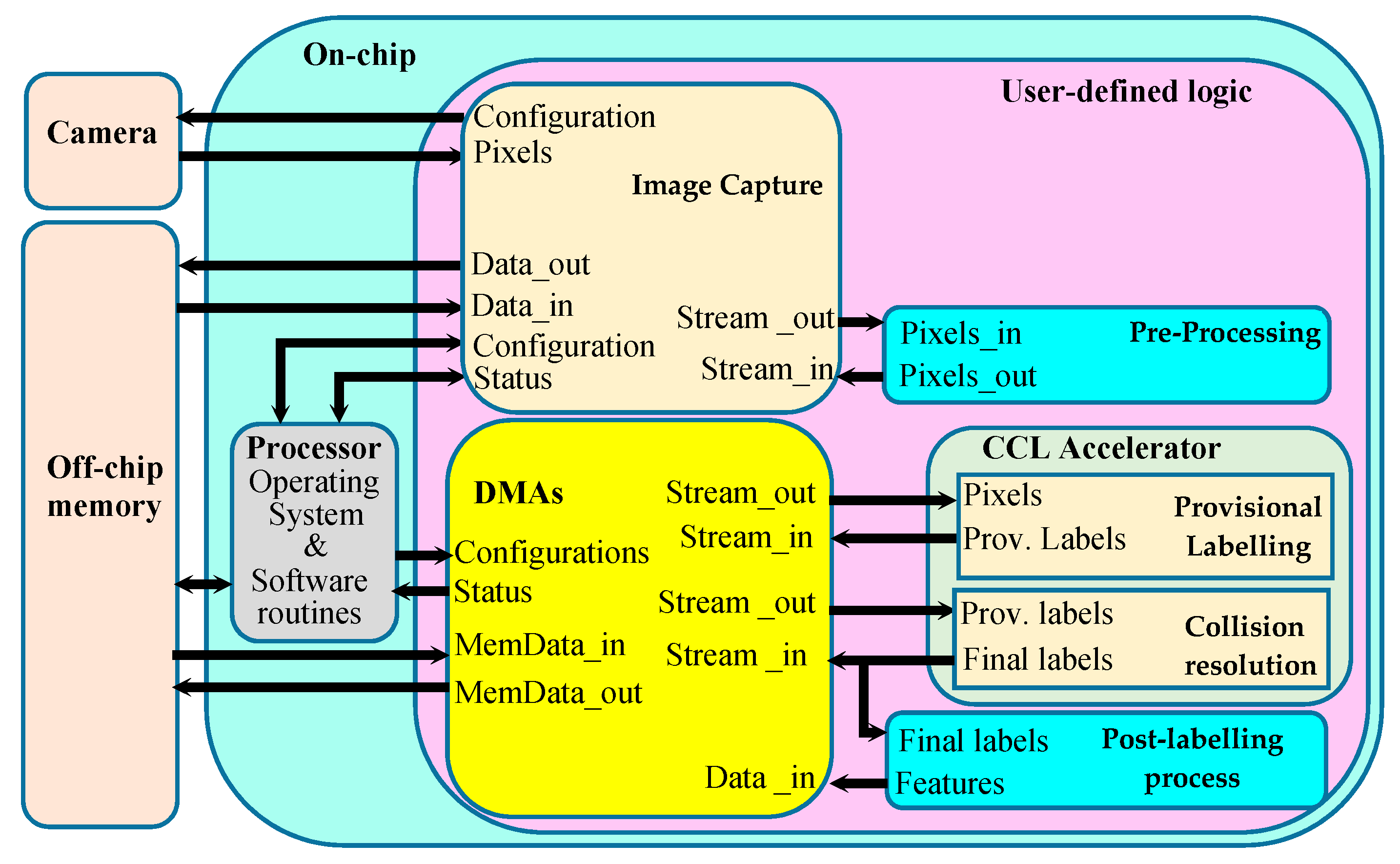
Some of the hardware architectures previously proposed for two-scan CCL methods were (or can be) integrated within heterogeneous image processing embedded systems, like that illustrated in Figure 1. There, the two main portions, consisting of a general-purpose processor and the user-defined logic, communicate with each other through an appropriate protocol. Typically, an external camera acquires the input image using the desired data format. The input pixels received by the image capture module are stored, if necessary, within an external memory and streamed to the pre-processing module that performs all the operations, like filtering, thresholding, binarization, etc., required to produce the image to be labeled. The latter is stored in the external memory and successively resumed to be streamed toward the CCL accelerator. In the meantime, the image capture acquires the next input frame and the pre-processing module prepares it for the labeling. The CCL and the eventual subsequent computation on the labeled image are hardware-implemented together with the Direct Memory Access (DMA) cores that are responsible for the data transfers to/from the external memory, which also stores the labeled output images.
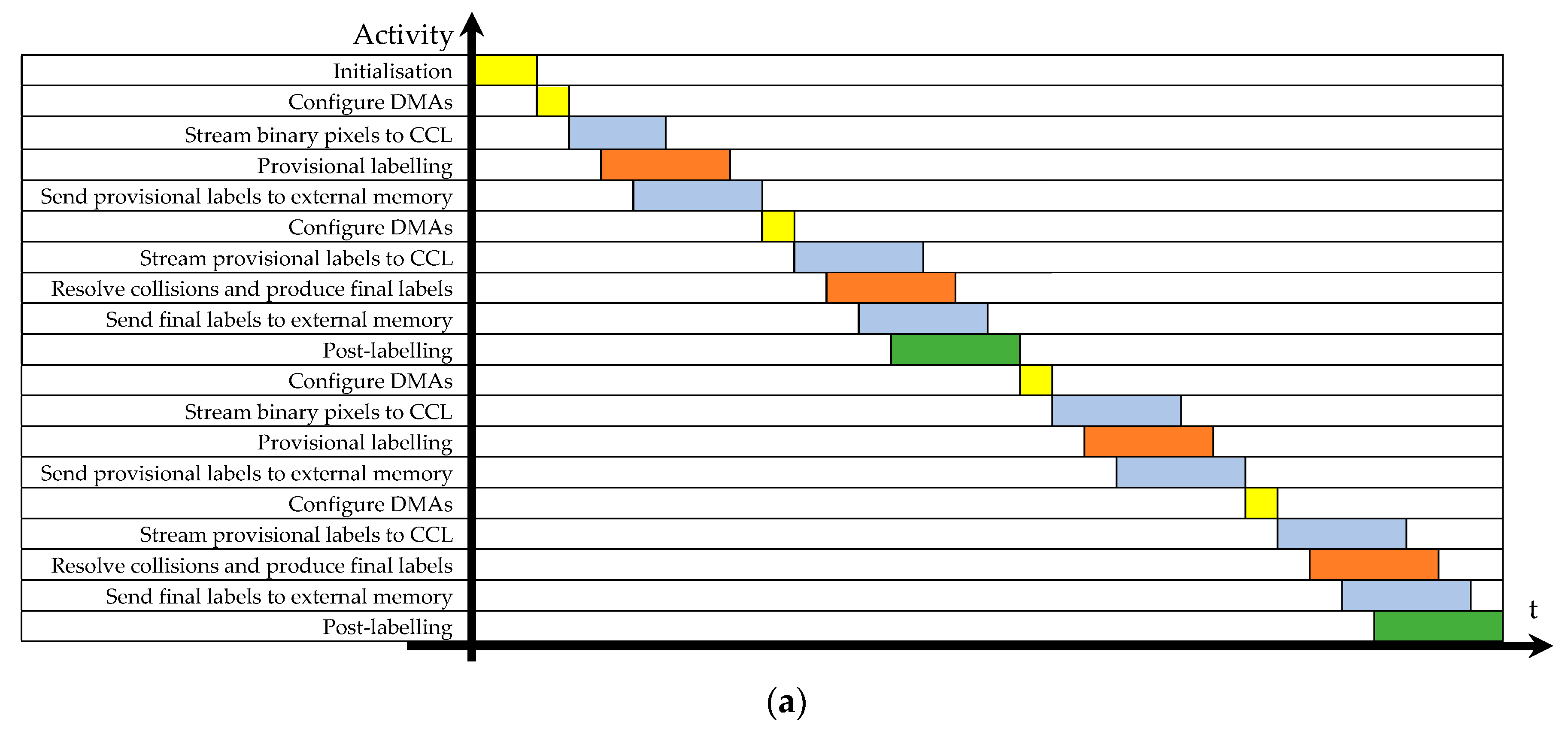
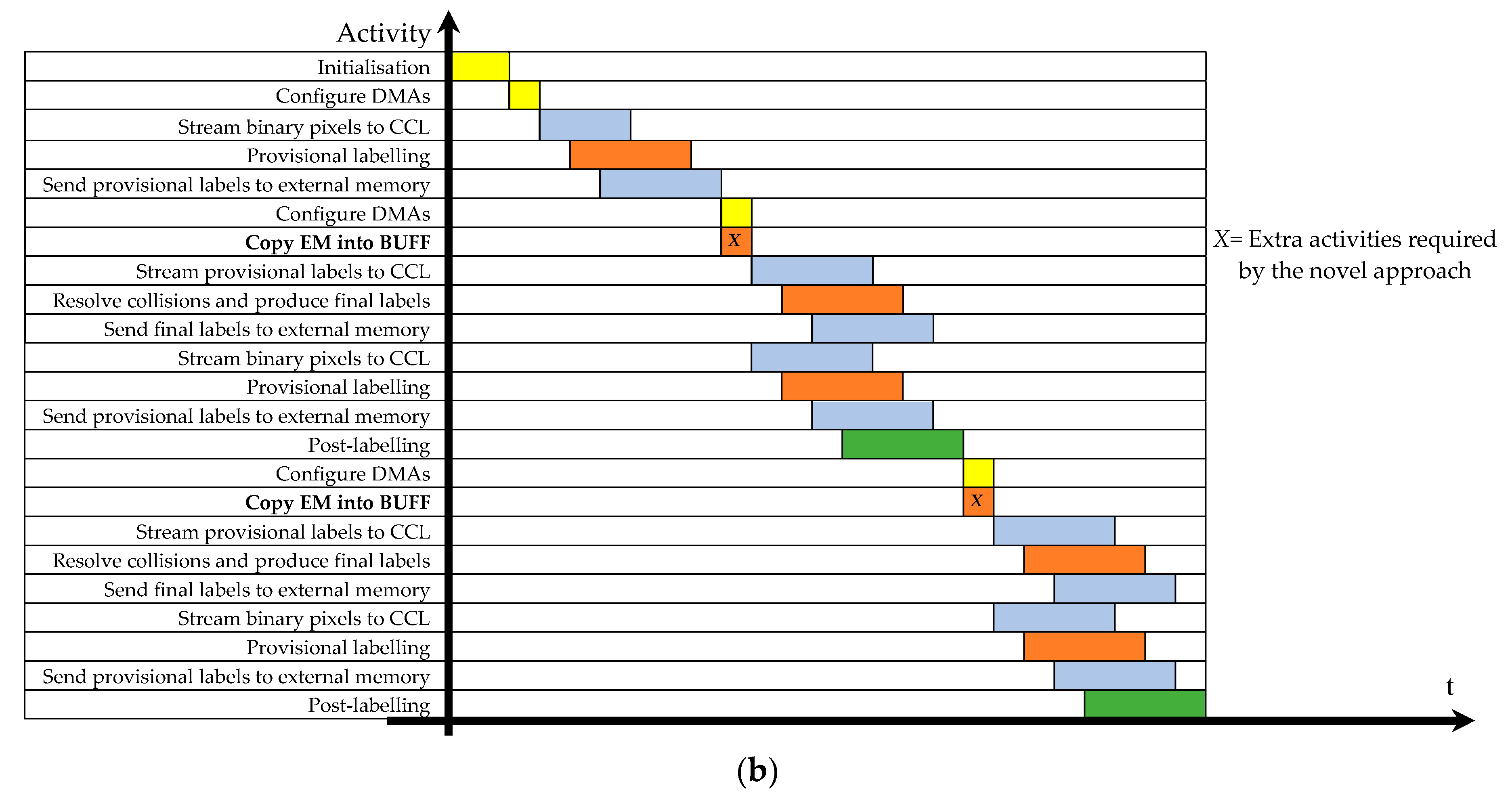
The main activities of such a designed embedded system are schematized in Figure 2a, which shows salient steps performed by each module over time to process two consecutive input binary images. After the initialization, the processor executes software routines responsible for managing, among others, the activity of DMAs. The DMAs are configured to specify which off-chip memory areas must be accessed in read and write modes during data transfers. The DMAs then stream binary input pixels to the CCL accelerator and collect provisional labels in the off-chip memory. The subsequent configuration instructs the DMAs to read (write) provisional (final) labels from (to) the external memory. Then, provisional labels are streamed toward the CCL, which resolves collisions and furnishes the final equivalent labels within a pattern-dependent time. If required, these labels can be further processed; then, the same activities are repeated for each subsequent input image. With respect to the above activity diagram, the approach proposed in Reference [18] has the merit of overlapping the operations required to resolve collisions with the second DMA configuration. Moreover, the presence of a label-translator LUT makes the architecture able to produce the final labels of the k-th input binary image and the provisional labels of the (k + 1)-th input image in parallel, thus significantly increasing the achievable frame rate. However, the use of a two-dimensional (2D) register array limits to few hundreds the number of labels that can be provisionally assigned.
3. The Proposed Labeling Architecture
The novel labeling architecture here proposed is designed to scan the input image in raster order. For simplicity, the case in which it elaborates couples of adjacent binary pixels to assign two adjacent provisional labels contemporaneously is detailed below. However, the novel approach can support even higher parallelism levels in accordance with the hardware platform used. As shown later, collisions are managed on the fly and the labels equivalences are updated, preventing long collision chains. In contrast to state-of-the-art two-scan methods, the novel approach is characterized by a collision resolution step that is pattern-independent, thus being much faster than traditional methods. Moreover, as illustrated in the activity diagram reported in Figure 2b, the provisional labeling and the calculation of final labels are performed concurrently on different input data. By comparing the activity diagrams in Figure 2, it is clear that the benefit attainable over a conventional design in terms of computational time is quite significant. To achieve the above advantages, label equivalences recognized during the provisional labeling are properly collected within two data structures, namely the translator LUT (TL) and the equivalence memory (EM), which allow the proposed architecture to operate in a pipeline fashion. At the end of the provisional labeling, the equivalences recorded in EM are stored into a buffer memory (BUFF) within a time depending just on the maximum number of labels (NLAB) manageable by the CCL architecture, as established at the design time. As visible in Figure 2b, this operation overlaps with the one-DMA configuration. Then, the buffer is read to assign the final correct labels, and, in the meantime, the next input image is provisionally labeled.
In Section 3.1, the proposed approach is detailed. Some examples are provided for both the four-connected and the eight-connected neighborhoods. For the latter, the further advantage of preventing the presence of more than two colliding labels is also achieved.
3.1. The Basic Rules
The provisional labeling assigns the label zero to each background pixel within the input binary image and associates with each foreground pixel P(i,j) the proper label depending on its neighborhood. The proposed approach manages the three possible conditions occurring for a foreground pixel as explained below.
- If P(i,j) is surrounded by background pixels, it receives a new label Ln (with Ln = 1, …, NLAB − 1), and this event is recorded in TL by storing TL(Ln) = Ln and, at the same time, EM(Ln) = Ln.
- If the current neighborhood contains just one foreground pixel already labeled as Lx, then P(i,j) is provisionally labeled with TL(TL(Lx)), without updating TL and EM.
- If the neighbors are associated with two colliding labels Lu and Ll, P(i,j) is provisionally labeled with Lmin = TL(min(TL(Lu),TL(Ll))). Moreover, the newly identified equivalence is recorded in TL by storing TL(max(TL(Lu),TL(Ll))) = min(TL(Lu),TL(Ll)). At the same time, with Lmax = TL(max(TL(Lu),TL(Ll))), the equivalences EM(Lmax) and EM(Lmin) are resumed to update EM by storing both EM(EM(Lmax)) = EM(Lmin) and EM(Lu) = EM(Lmin).
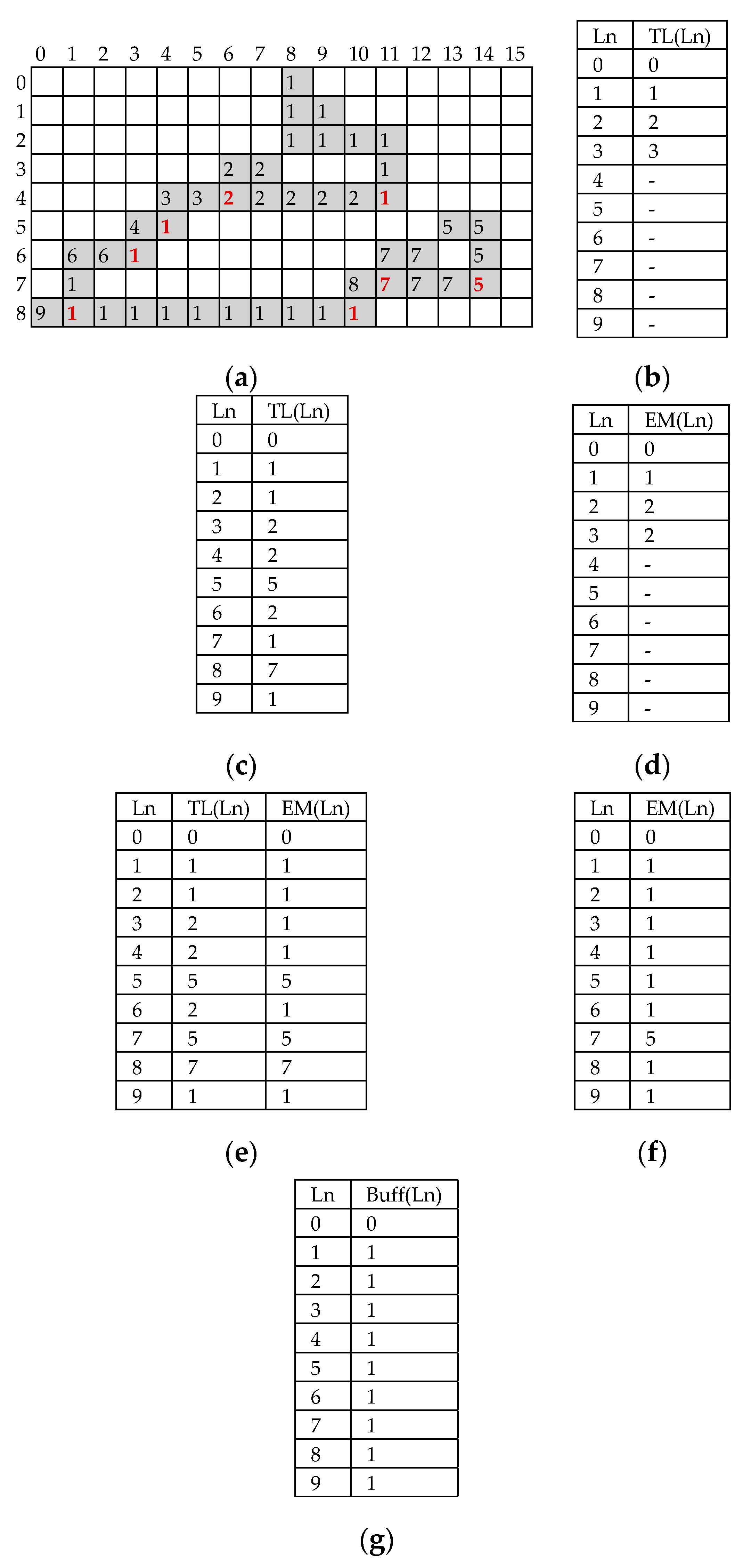
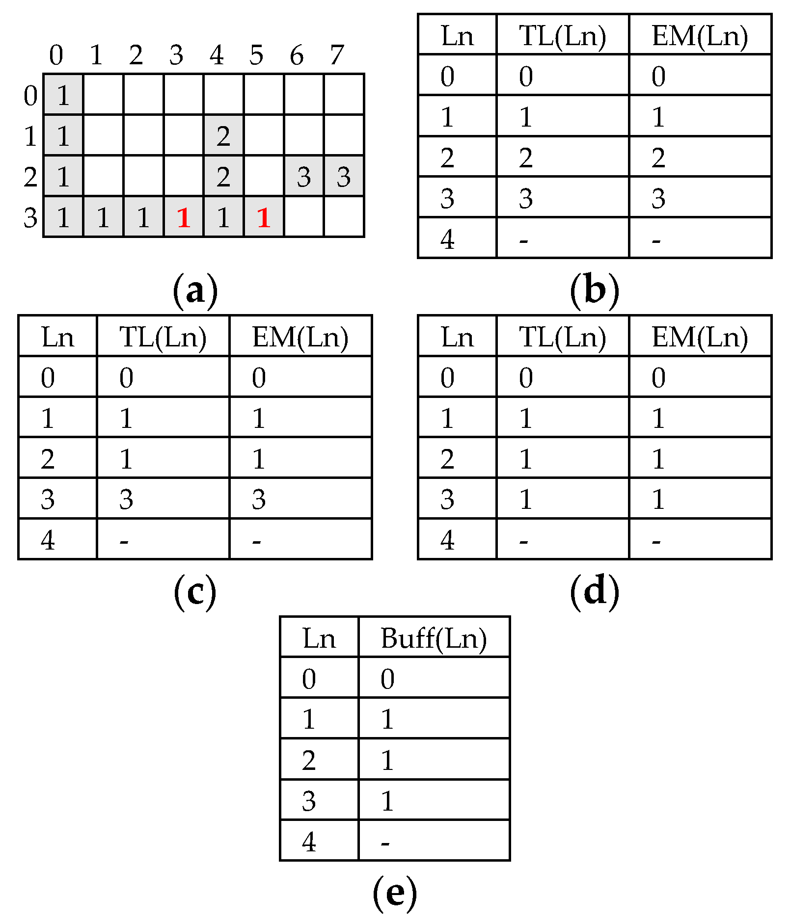
It is worth noting that the above rules allow a label equivalence to be always immediately propagated and complex chains of colliding labels to be prevented. More exactly, independently of the processed frame, at the end of the provisional labeling, the annotated chains of collisions can never be longer than two. To better explain how the proposed provisional labeling runs, let us suppose that the binary image illustrated in Figure 3a, where foreground and background pixels are colored grey and white, respectively, is being labeled referring to the four-connected neighborhood. The pixels preceding P(4,6) are provisionally labeled as visible in Figure 3a by applying the rules above given for cases 1 and 2. When pixel P(4,6) is reached, TL contains the information reported in Figure 3b. The neighborhood of P(4,6) contains two foreground pixels associated with the colliding labels Ll = 3 and Lu = 2 that are yet to collide with other labels and, therefore, TL(TL(Ll)) = 3 and TL(TL(Lu)) = 2. As ruled above for case 3, P(4,6) is provisionally labeled with TL(2) = 2, and TL is updated by storing TL(3) = 2. Similar conditions occur for all the subsequent collisions highlighted with bold characters. At the end of the image scan, TL contains the information reported in Figure 3c. The latter clearly shows that, as expected, the most complex chains of colliding labels annotated during the provisional labeling into TL are no longer than two. As an example, this is the case for the chains 8→7→1 (i.e., the label 8 is equivalent to the label 7, which in turn is equivalent to the label 1), 3→2→1, and so on. During the provisional labeling, EM also has to be initialized and updated. When the first collision is encountered at the pixel P(4,6), since Lu = 2 and Ll = 3, Lmax = TL(3) = 3 and Lmin = TL(2) = 2. Therefore, as shown in Figure 3d, EM is updated by storing EM(EM(3)) = 2 and EM(2) = 2. The need for also updating the value EM(Lu) becomes clear upon analyzing the last collision occurring for the pixel P(8,10). When it is reached, TL and EM contain the equivalences reported in Figure 3e and must be then updated. Since Lu = 8, Ll = 1, Lmax = 7, and Lmin = 1, label 1 is written in both entries TL(7) and EM(EM(7)) = EM(5), thus immediately propagating the newly recognized equivalence. By updating EM(Lu) with EM(Lmin), i.e., making EM(8) equal to 1, the collision chain 8→7→5→1 is resolved on the fly and the simple chain 8→1 is annotated in its place. At the end of the provisional labeling, EM contains the labels equivalences visible in Figure 3f, with the longest collision chain being 7→5→1. This result clearly differs from that achievable by the previously described traditional two-scan algorithm. Indeed, when the latter is executed on the same benchmark image of Figure 3a, at the end of the provisional labeling, the worst unresolved collisions chain is six equivalences long.
Now, let us consider the binary image illustrated in Figure 4a and let us suppose that it is being labeled referring to the eight-connected neighborhood. The pixels preceding P(3,3) are provisionally labeled as visible in Figure 4a. When the pixel P(3,3) is reached, TL and EM contain the information reported in Figure 4b. The colliding labels Ll = 1 and Lu = 2 are yet to collide with other labels and, therefore, TL(TL(Ll)) = 1 and TL(TL(Lu)) = 2. As ruled above for case 3, P(3,3) is provisionally labeled with TL(1) = 1. Consequently, TL and EM are updated as shown in Figure 4c. When the pixel P(3,5) is reached, the labels L1 = 1, L2 = 2, and L3 = 3 are within the neighborhood. However, since TL(2) = 1, just the two labels Ll = 1 and Lu = 3 actually collide. Therefore, TL and EM are updated as illustrated in Figure 4d. It is worth noting that, in this case, a conventional provisional labeling should manage three colliding labels.
In order to improve the achievable throughput, the memory BUFF is exploited. It stores the final equivalent labels obtained as EM(EM(Ln)), with Ln ranging from 0 to NLAB − 1. Figure 3g and Figure 4e illustrate its final content for the above examples. In this way, the second scan for the final labeling of an input frame can be performed in parallel with the provisional labeling of the subsequent frame.
As discussed below, the above-described labeling strategy can also be parallelized, and multiple labeled pixels can be output at each clock cycle. When two pixels are processed contemporaneously, taking into account all the above considerations, it can be affirmed that the proposed parallel CCL approach completes the connected component labeling over an n × m binary image within only n × m + NLAB clock cycles. images are needed to perform the provisional labeling; NLAB cycles are required to store the final equivalent labels in the memory BUFF; finally, cycles are spent to complete the final labeling. Consequently, a throughput close to two pixels per clock cycle is expected.
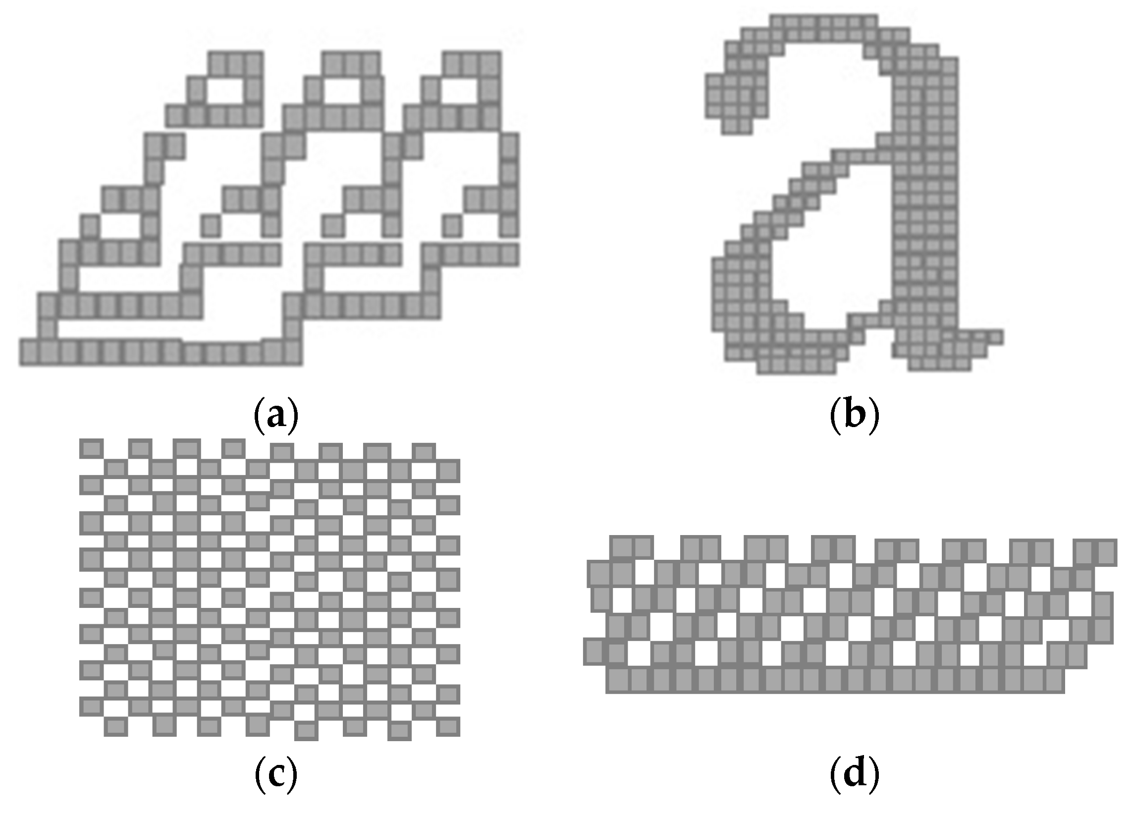
Figure 5 illustrates benchmark images much more critical than that previously examined. Patterns shown in Figure 5a,b contain complex single connected components with very long collision chains. On the contrary, patterns depicted in Figure 5c,d require a high number of labels (NL) to be assigned during the provisional labeling and/or a high number of collisions (NC) to be managed.
In general, for an n × m input image, NL is at most equal to [2], while, when four-connected neighborhoods are referenced, NC can be equal at most to . However, these critical conditions can occur only separately and in the presence of artificial images. As a nice side effect, the novel parallel CCL approach allows reducing both NL and NC, thus allowing complex connected components to be treated, restricting both depth and width of TL, EM, and BUFF.
3.2. Introducing the Parallelism
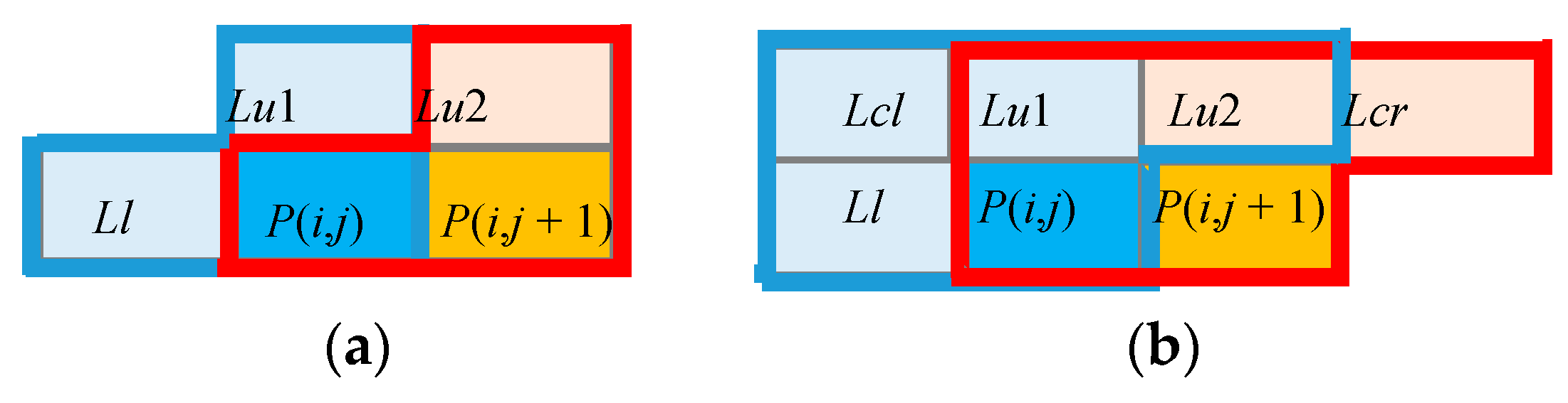
As anticipated above, the proposed architecture is able to elaborate two adjacent input pixels (P(i,j) and P(i,j + 1)) per clock cycle and to produce two labeled output pixels without requiring irregular accesses to the external memory. To perform such a parallel action, the neighborhoods of two adjacent input pixels illustrated in Figure 6 are processed concurrently. Obviously, if both P(i,j) and P(i,j + 1) are background pixels, both output labels are set to zero. All other possible cases, occurring within a four-connected neighborhood, are treated as shown in Table 1. There Lu1, Lu2, and Ll are the provisional labels already assigned to the neighboring pixels; L(i,j) and L(i,j + 1) are the two provisional labels currently assigned to the input pixels; finally, Update TL and Update EM are the operations performed to update TL and EM, respectively.
It can be seen that, if P(i,j) is a background pixel, L(i,j) is certainly zeroed and L(i,j + 1) depends on the label Lu2; thus, only cases 1 and 2, listed in Section 3.1, can occur around P(i,j + 1). On the contrary, when P(i,j) and P(i,j + 1) are foreground and background pixels, respectively, a collision can also take place. Even though, as illustrated in Figure 6a, the analyzed neighborhood contains three labels, only two of them (i.e., the bolded and underlined ones in Table 1) can actually collide. In fact, being adjacent, the labels Lu1 and Lu2 are either equal or they differ from each other with one of them being zero, thus causing either case 3 or case 2 of Section 3.1 to occur. The same consideration can be done for the cases in which both P(i,j) and P(i,j + 1) are foreground pixels.
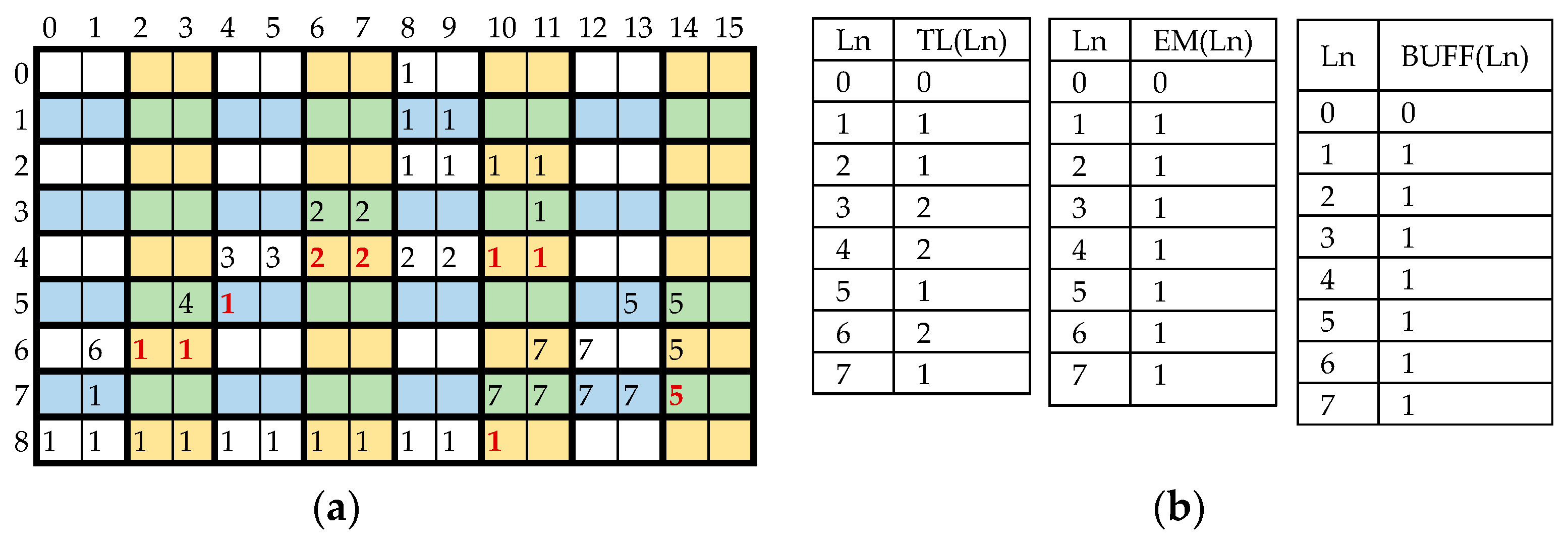
By applying the proposed method to the benchmark pattern of Figure 3a, the resulting provisionally labeled output appears quite different. It is depicted in Figure 7a, where different colors are used to highlight couples of labels elaborated in parallel. It can be easily observed that, due to the parallel action, the number NL of provisional labels used is seven instead of nine, and the number NC of collisions encountered is six instead of eight. At the end of the provisional labeling, TL and EM contain the information depicted in Figure 7b. The final labels are then collected in BUFF.
Table 2 collects the possible cases occurring when two adjacent eight-connected neighborhoods are processed in parallel. In this case, the labels Lcl and Lcr are also taken into account, since, as depicted in Figure 6b, they are associated with the pixels P(i − 1,j − 1) and P(i − 1,j + 2), respectively. Moreover, the symbol x is used to indicate the “do not care” condition. It can be seen that, since the labels equivalences recognized during the provisional labeling are immediately propagated, as within two adjacent eight-connected neighbourhoods, at most two colliding labels can be encountered.
4. The Hardware Architecture of the Novel Parallel Labeling Approach
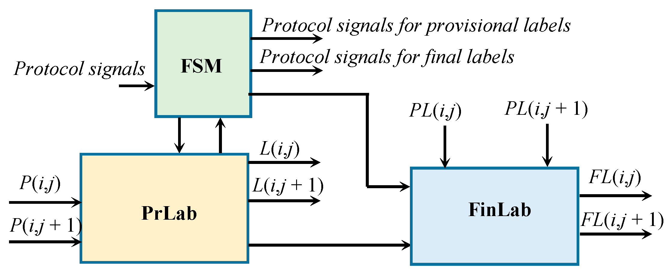
This section presents a hardware accelerator purpose-designed to exploit the novel parallel labeling method with four-connected neighborhoods. Figure 8 illustrates the top-level architecture of the proposed parallel CCL core. The main computational modules PrLab and FinLab are responsible for the provisional and the final labeling steps, respectively. The finite state machine (FSM) orchestrates the overall running, by dispatching to the computational modules the proper control signals that, based on the communication protocol adopted to manage input and output data transfers, validate input and output data and flag that the incoming (out coming) datum is the last one, and so on.
In Figure 8, it is assumed that two pixels are processed contemporaneously. However, the maximum parallelism level, exploitable without compromising the throughput actually achieved, could be increased in accordance with the resources and the transfer capability provided by the used realization platform. As an example, in the implementations carried out using the Xilinx XC7Z020 and XC7Z045 devices, the proposed design streams output at most two 10-bit labeled pixels paired within a 20-bit word at each clock cycle (this happens when 1024 labels are handled). In this case, the capability supported on-chip [34] to transfer data to/from the external memory would allow up to six labeled pixels to be furnished in parallel at each clock cycle, achieving the maximum throughput rate. Conversely, more than six labeled pixels would be packed within data words wider than 64-bit, thus making multiple clock cycles necessary for each data transfer [34]. Obviously, this means that a parallelism higher than six would not yield the expected benefits, since the actual throughput would not be maximized. Similar considerations also apply to other hardware platforms.
The proposed architecture can be integrated as a custom accelerator within state-of-the-art FPGA-based SoCs, like that depicted in Figure 1. In such an implementation platform, the binary input image to be labeled is stored in the raster order within the off-chip memory. Each pixel is accommodated in an 8-bit word memory location. Therefore, to accomplish the parallel input data flow, two adjacent input pixels (i.e., two contiguous memory locations) have to be resumed per clock cycle. For this purpose, a proper software configuration of the DMAs is necessary to set the input data word to 16-bit. In a similar way, the DMAs can be configured to transfer toward the external memory two adjacent labeled pixels packed within one -bit word, with ) and NLAB being the maximum number of manageable labels established at the design time. The two adjacent labels are then automatically stored within contiguous memory locations.
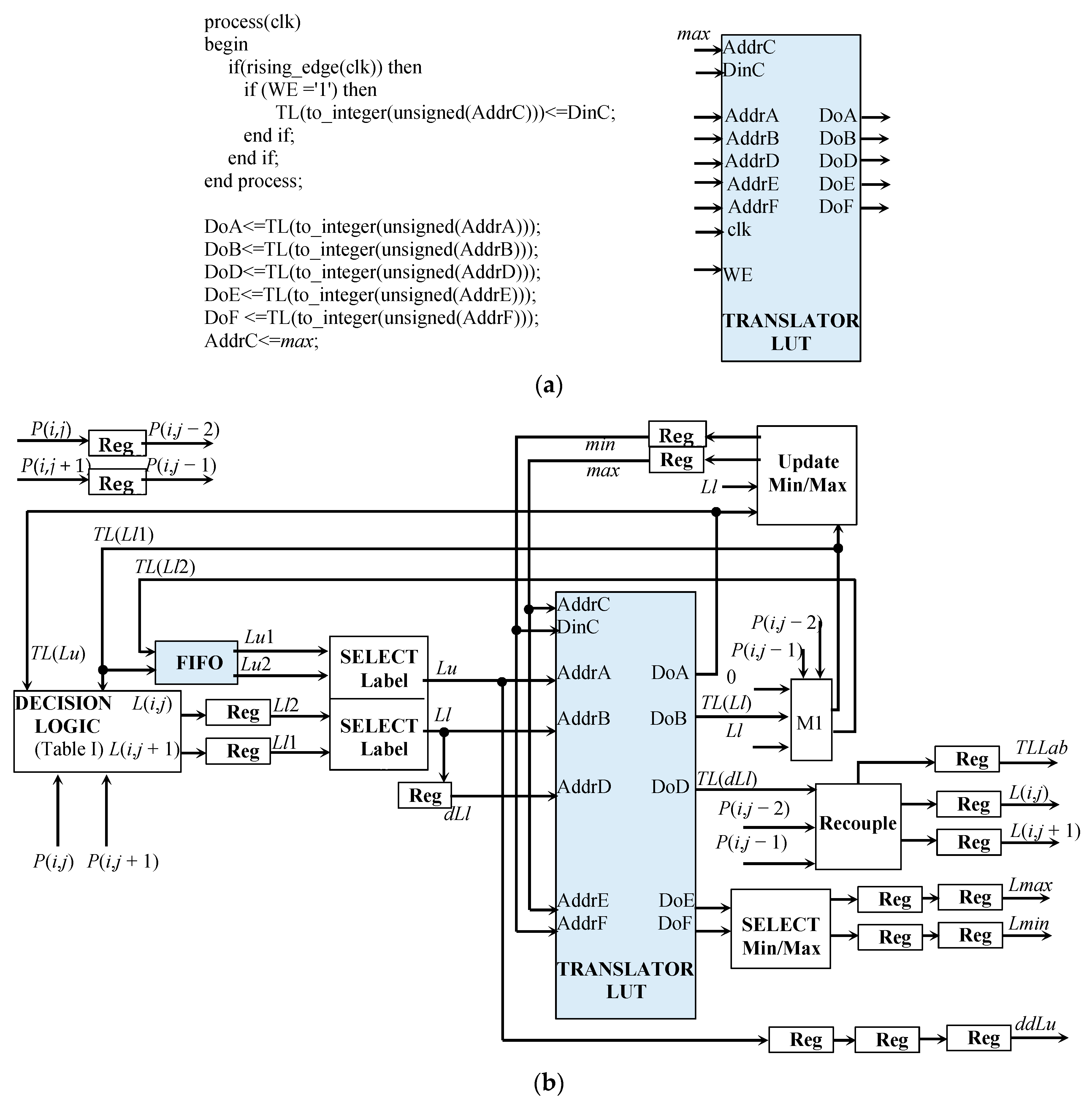
The hardware architecture of the PrLab module includes the portion implementing the translator LUT update and the equivalence memory management system illustrated in Figure 9 and Figure 10, respectively. These circuits use a proper amount of registers (Regs) to execute their actions in a pipeline fashion.
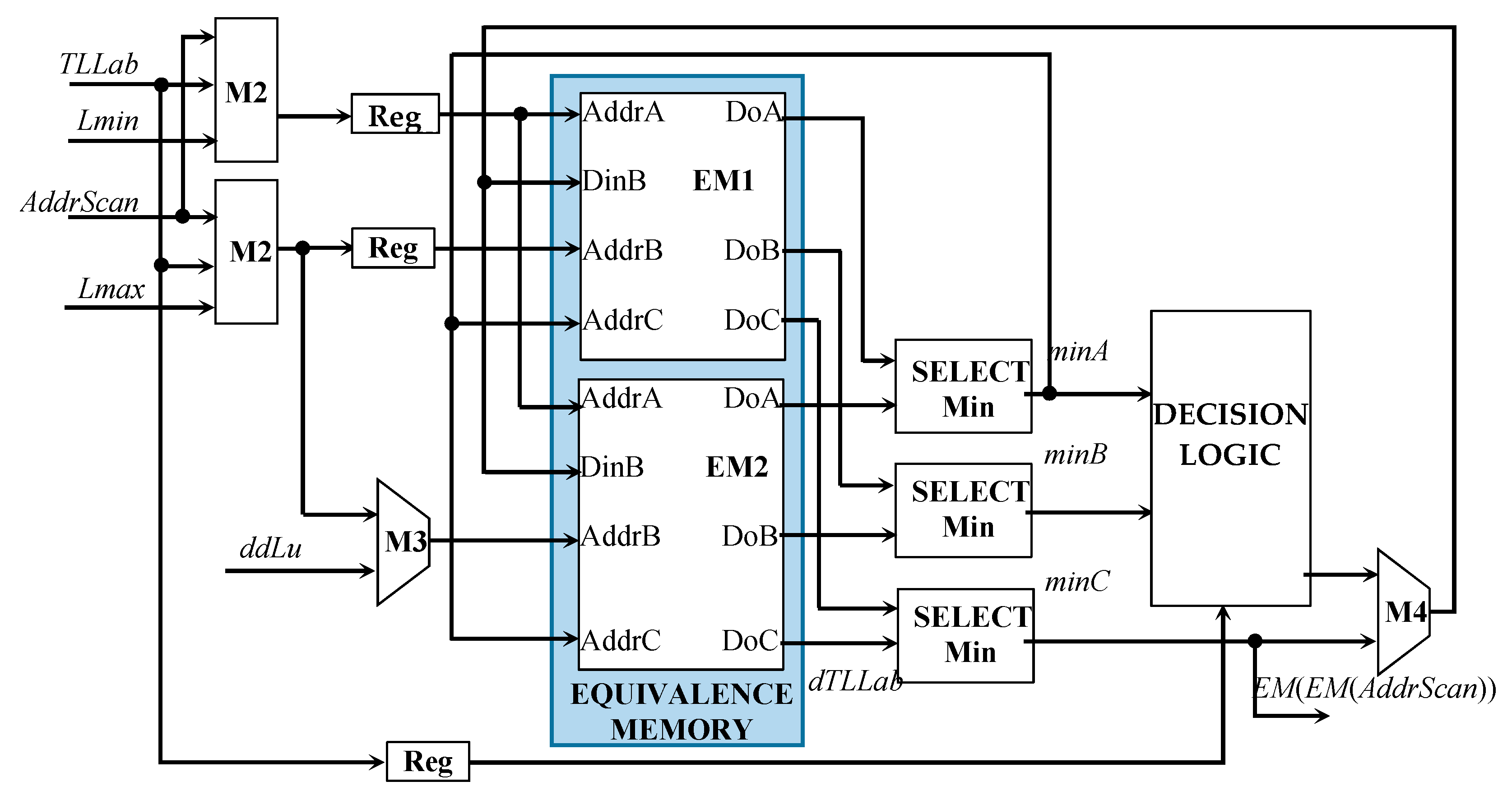
Both TL and EM exploit multiport memory banks with proper access policies. In fact, to comply with the process described in Section 3.1, TL must sustain two read and one write accesses, concurrently. Conversely, to update EM, two accesses in read mode and two in write mode are needed. To support such an activity, EM consists of two mirror stages (EM1 and EM2). They share the signals driving the read ports, while each one receives its own signals to drive the address write ports.
To implement both TL and EM, distributed memory resources based on LUT primitives were exploited. Indeed, they allow multiple asynchronous read and one synchronous write operations to be performed in the same clock cycle [35]. Figure 9a sketches how the Very high-speed integrated circuits Hardware Description Language (VHDL) code manages the multiple accesses to TL. It can be seen that the read-first access policy is adopted to solve eventual read–write conflicts.
From Figure 9b, it can be seen that, with i being the currently scanned image row, the First-In First-Out (FIFO) module is used to locally store the provisional labels already assigned to the pixels belonging to the (i − 1)-th row, thus ensuring that the neighborhoods of the current input pixels P(i,j) and P(i,j + 1) are correctly formed. Since two adjacent pixels are processed in parallel, and then two adjacent nb-bit provisional labels are assigned at the same time, the FIFO must stack -bit words. The modules SELECT label are used to exploit the property for which adjacent pixels are either equally labeled or one of them is zero-labeled. Therefore, only Lu and Ll are actually processed instead of the labels Lu1, Lu2, Ll1, and Ll2 (where Ll2 and Ll1 are the provisional labels assigned to P(i,j − 2) and P(i,j − 1) at the previous step), thus removing redundant operations.
Before being input to the decision logic, the provisional labels Lu and Ll are translated to immediately exploit already known labels equivalences. In order to do this, Lu and Ll are used to access TL through the read ports A and B. On the basis of the nb-bit label TL(Ll) and the previously received pixels P(i,j − 1) and P(i,j − 2), the simple circuit M1 forms the two nb-bit translated labels TL(Ll1) and TL(Ll2) that are delivered toward the FIFO and the decision logic module. In the case of a collision, the minimum and maximum values min and max between TL(Lu) and TL(Ll) are computed by the module update min/max. Then, they are used to update the labels equivalences through the write port C. Conversely, when Ll is a new label, the module update min/max furnishes min = max, thus storing TL(Ll) = Ll. Finally, the module recouple reconstructs the two nb-bit labels provisionally assigned to the processed pixels on the basis of TL(dLl) and taking into account that adjacent labels either are equal or differ, with one of them being zero. Conversely, the provisional label TLLab and the labels Lmax, Lmin, and ddLu are forwarded to the subsequent module to initialize and update EM. The provisional labels L(i,j) and L(i,j + 1) are delivered toward the external memory to be subsequently uploaded for the final labeling.
Figure 10 illustrates the equivalence memory management circuit. When TLLab is a valid propagated label assigned without encountering a collision, the values EM(Lmin) and EM(Lmax), resumed through the ports A and B of EM1 and EM2, are made available as the signals minA and minB, respectively. The ports B of both EM1 and EM2 are then used in write mode to set EM(Lmax) = EM(Lmin) (i.e., EM(Lmax) is made equal to minA). However, since, in the above-examined case, TLLab is not the result of a collision, Lmax and Lmin are certainly equal. Thus, the content of EM remains unchanged. Otherwise, in the presence of a collision, Lmax and Lmin differ from each other. In this case, the write operations performed through the ports B of EM1 and EM2 change the values stored in the entries EM(Lmax) and EM(ddLu), respectively, thus actually updating EM as expected.
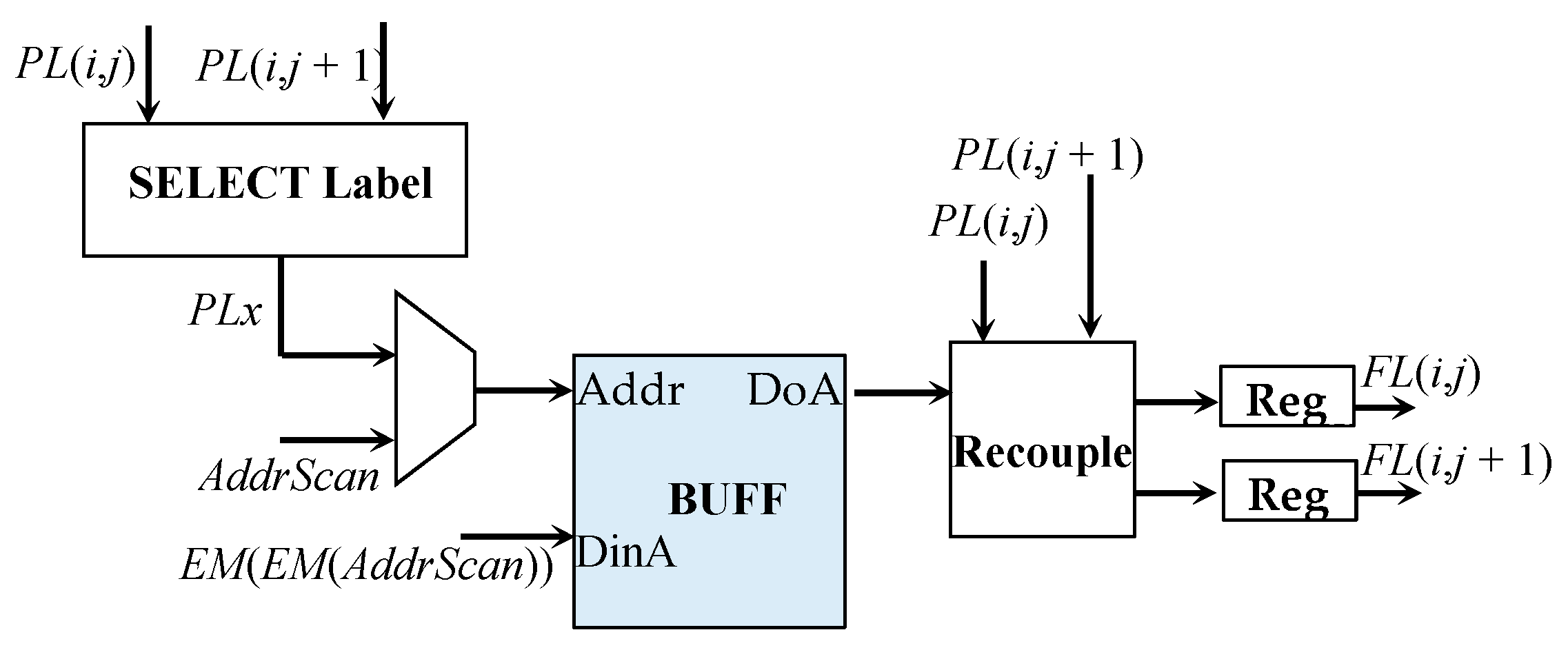
At the end of the provisional labeling, EM is scanned, and the resolved equivalences are stored within the buffer memory BUFF contained in the FinLab module depicted in Figure 11. The signal AddrScan is used to access BUFF in write mode. As visible in Figure 10, the AddrScan signal reaches, through M2, the ports A of EM1 and EM2 that are used in read mode to resume EM(AddrScan), which is made available as the signal minA. The latter is then used to read EM1 and EM2 through the ports C, thus uploading EM(EM(AddrScan)) on the signal minC.
When all the above steps are completed, the second scan that assigns the final labels to recognize connected components is performed. During this phase, the FinLab module receives two adjacent provisional labels PL(i,j) and PL(i,j + 1) in parallel as input and the module SELECT label simply establishes which one must feed the address port for reading BUFF. The final labels FL(i,j) and FL(i,j + 1) are then provided by the module recouple that, on the basis of PL(i,j) and PL(i,j + 1), establishes whether FL(i,j) and FL(i,j + 1) are equal or one of them is zero.
5. Results
The core of the above architecture was designed in VHDL. It was endowed with the auxiliary circuitry required to comply with the AXI4 protocol [33]. Therefore, it can be directly included within image processing embedded systems realized with state-of-the-art Xilinx [34] or Intel [36] FPGA-based SoCs. Xilinx devices were chosen for the purpose of prototyping, and they are referenced below.
Speed performances and resources requirements were analyzed for image sizes ranging from 640 × 480 to 2k × 2k with NLAB varying between 64 and 8192. Table 3 summarizes the obtained results in comparison with state-of-the-art competitors. Several implementations were characterized on various devices in terms of running frequency, number of pixels labeled per clock cycle (ppcc), frame rate (fps), and resource requirements. For purposes of comparison, two specific implementations that exploit the design principle demonstrated in Reference [18] were also realized and characterized.
As expected, even though the multiple asynchronous memory accesses performed per clock cycle to update TL and EM limit the running frequency, the gain due to the parallel actions at both the pixel and frame level allowed frame rates significantly higher than the referenced counterparts to be achieved. This result was obtained with very limited resource requirements. From Table 3, it is easy to verify that the requirement of on-chip RAM and the amount of LUTs configured either as logic or as RAM only depend on NLAB. Conversely, the amounts of FFs and LUTs configured as shift registers mainly depend on the input image size.
To fairly compare the various architectures, the resource efficiency metric ResEFF was evaluated, as given in Equation (1) [6]. There, the amount of occupied logic resources (Res) is expressed in terms of the kbits required to account the contributions of LUTs, FFs, and Block RAMs (BRAMs). It was calculated considering that the Xilinx Series-7 and the Virtex-6 technologies provide six-input LUTs, whereas Virtex-2, Virtex-4, and Stratix EP1S25 devices provide four-input LUTs. Obviously, a higher ResEFF results in a more efficient circuit.
Just as an example, let us compare the behavior of the design presented in Reference [22] with the corresponding implementation proposed here and realized on the XC7Z020 device. Both operate on 2k × 2k input images and manage 1024 labels. Despite a similar clock frequency, the novel design reaches a frame rate more than double with respect to Reference [22], by using only 10 kbits of RAM instead of the 400 kbits required in Reference [22]. Therefore, the corresponding ResEFF ratio is ~4.72.
For comparison with the system proposed in Reference [14], the novel CCL architecture was prototyped using the same XC7VX1140T device for the input image resolution of 2k × 1.5k. The circuit in Reference [15] manages at most 7156 labels, operates at the 300 MHz clock frequency, thus achieving a maximum frame rate of ~39 fps, and requires 2592 kbits of RAM. The novel architecture runs at 73.2 MHz, achieves a frame rate ~19% higher than Reference [15], and requires only 104 kbits of RAM, thus exhibiting a ResEFF more than eight times higher.
Similar conclusions can be drawn for other competitors. It is worth noting that some of them were realized as standalone modules; thus, their figures do not account for auxiliary communication circuitry.
Several hardware tests performed using the ZedBoard prototyping board [37] confirmed the correct running of the novel CCL accelerator. Post-implementation results show that, as an example, with the hardware accelerator and the application software running at the 88 MHz and the 666 MHz operating frequency, respectively, when NLAB = 128, a 640 × 480 input image is completely labeled within less than 1.75 ms. In this case, the novel CCL accelerator dissipates only ~7.5 mW.
It is finally remarkable that the proposed CCL approach can be exploited to realize a hardware accelerator compatible with the 4 K Ultra High Definition (4K/UHD) video stream. In this case, a high-end platform, like the UltraScale+ [38] should be used to sustain the 60-fps frame rate. A draft evaluation showed that, using the Xilinx Zynq UltraScale+ ZU3EG MPSoC device, the operating frequency reached when NLAB = 8192 would be slightly higher than 150 MHz. Therefore, a parallelism level equal to four would allow completely labeling a 3840 × 2160 input frame within only 13.8 ms, which suffices to reach the target 60 fps.
To provide the reader with a “big picture”, the peculiar characteristics of some representative one-scan CCA methods are also collected in Table 4. It can be seen that the architectures presented in References [6] and [9] are able to extract the area (i.e., the number of pixels) of connected components within the input image, whereas the designs proposed in References [7] and [8] provide their coordinates, i.e., the bounding boxes (BBs). The referred CCA solutions support different number of manageable labels, and they show different resource requirements and speed performances. The design presented in Reference [8] achieves the highest frame rate, but it occupies a significant amount of hardware resources to manage just 64 labels. On the other hand, the competitors manage more labels and achieve appreciable speeds with reasonable resource occupancy.
6. Conclusions
This paper presented a novel two-scan labeling approach, able to parallelize operations at both pixel level and frame level, as well as its custom hardware architecture. The proposed design elaborates two input binary pixels in parallel and provides two labeled pixels at once. Furthermore, to maximize the achievable throughput, the custom architecture allows overlapping the two scans across consecutive frames. Different implementation platforms, input image sizes, and number of treatable labels were referenced for purposes of comparison with most relevant prior works. Obtained results demonstrated that the proposed parallel CCL architecture can process up to 1.908 pixels per clock cycle, exhibiting a resource efficiency at least 4.7 times higher than existing counterparts. The proposed CCL architecture was accommodated within a complete heterogeneous embedded SoC processing high-resolution images. The performed tests demonstrated that at least 30.3 frames are processed per second, thus improving the frame rates achieved by state-of-the-art competitors, at a parity of image size, by ~51.5%.
Author Contributions
Conceptualization, S.P., F.S., and P.C.; formal analysis, S.P., F.S., and P.C.; investigation, S.P., F.S., and P.C.; writing—review and editing, S.P., F.S., and P.C. All authors have read and agreed to the published version of the manuscript.
Funding
This research received no external funding.
Conflicts of Interest
The authors declare no conflicts of interest.
References
- Ronsen, C.; Denjiver, P.A. Connected Components in Binary Images: The Detection Problem; Research Studies Press: New York, NY, USA, 1984. [Google Scholar]
- He, L.; Ren, X.; Gao, Q.; Zhao, X.; Yao, B.; Chao, Y. The connected-component labelling problem: A review of state-of-the-art algorithms. Pattern Recognit. 2017, 70, 25–43. [Google Scholar] [CrossRef]
- Kong, B.Y.; Lee, J.; Park, I.C. A Low-Latency Multi-Touch Detector Based on Concurrent Processing of Redesigned Overlap Split and Connected Component Analysis. IEEE Trans. Circ. Syst. I: Reg. Papers 2019, 1–11. [Google Scholar] [CrossRef]
- He, Y.; Hu, T.; Zeng, D. Scan-Flood Fill (SCAFF): An Efficient Automatic Precise Region Filling Algorithm for Complicated Regions. In Proceedings of the 2019 International Conference on Image Processing, Computer Vision, and Pattern Recognition, Long Beach, CA, USA, 16–20 June 2019. [Google Scholar]
- Hennequin, A.; Lacassagne, L.; Cabaret, L.; Meunier, Q. A new Direct Connected Component Labelling and Analysis Algorithms for GPUs. In Proceedings of the 2018 Conference on Design and Architectures for Signal and Image Processing, Porto, Portugal, 10–12 October 2018. [Google Scholar]
- Spagnolo, F.; Perri, S.; Corsonello, P. An Efficient Hardware-Oriented Single-Pass Approach for Connected Component Analysis. Sensors 2019, 19, 3055. [Google Scholar] [CrossRef] [PubMed] [Green Version]
- Tang, J.W.; Shaikh-Husin, N.; Sheikh, U.U.; Marsono, M.N. A linked list run-length-based single-pass connected component analysis for real-time embedded hardware. J. Real Time Image Process. 2018, 15, 197–215. [Google Scholar] [CrossRef]
- Klaiber, M.J.; Bailey, D.G.; Simon, S. A single-cycle parallel multi-slice connected components analysis hardware architecture. J. Real Time Image Process. 2019, 16, 1165–1175. [Google Scholar] [CrossRef]
- Ma, N.; Bailey, D.G.; Johnston, C.T. Optimised single pass connected components analysis. In Proceedings of the International Conference on Computer and Electrical Engineering, Taipei, Taiwan, 8–10 December 2008. [Google Scholar]
- Grana, C.; Borghesani, D.; Cucchiara, R. Optimized Block-based Connected Components Labelling with Decision Trees. IEEE Transact. Image Process. 2010, 19, 1596–1609. [Google Scholar] [CrossRef] [PubMed] [Green Version]
- Di Stefano, L.; Bulgarelli, A. A simple and efficient connected component labelling algorithm. In Proceedings of the 10th International Conference on Image Analysis and Processing, Venice, Italy, 27–29 September 1999. [Google Scholar]
- Zhao, C.; Duan, G.; Zheng, N. A Hardware-Efficient Method for Extracting Static Information of Connected Component. J. Signal Process. Syst. 2017, 88, 55–65. [Google Scholar] [CrossRef]
- Asano, T.; Buzer, L.; Bereg, S. A new algorithm framework for basic problems on binary image. Discr. Appl. Mathem. 2017, 216, 376–392. [Google Scholar] [CrossRef]
- Appiah, K.; Hunter, A.; Dickinson, P.; Meng, H. Accelerated hardware video object segmentation: From foreground detection to connected components labelling. Comput. Vis. Image Underst. 2010, 114, 1282–1291. [Google Scholar] [CrossRef] [Green Version]
- Zhao, C.; Gao, W.; Nie, F. A Memory-Efficient Hardware Architecture for Connected Component Labelling in Embedded System. IEEE Trans. Circ. Syst. Video Tech. 2019. [Google Scholar] [CrossRef]
- Teich, J. Hardware/Software Codesign: The Past, the Present and Predicting the Future. Proc. IEEE 2012, 100, 1411–1430. [Google Scholar] [CrossRef]
- Farhat, W.; Faiedg, H.; Souani, C.; Besbes, K. Real-time embedded system for traffic sign recognition based on ZedBoard. J. Real Time Image Process. 2017, 1–11. [Google Scholar] [CrossRef]
- Spagnolo, F.; Frustaci, F.; Perri, S.; Corsonello, P. An Efficient Connected Component Labelling Architecture for Embedded Systems. J. Low Power Electron. Appl. 2018, 8, 7. [Google Scholar] [CrossRef] [Green Version]
- Schwenk, K.; Huber, F. Connected Component Labelling Algorithm for very complex and high resolution images on FPGA platform. Proc. SPIE 2015, 9646, 1–14. [Google Scholar]
- Chang, F.; Chen, C.J. A component-labelling algorithm using contour tracing technique. Comput. Vis. Image Underst. 2004, 93, 206–220. [Google Scholar] [CrossRef] [Green Version]
- Hedberg, H.; Kristensen, F.; Owall, V. Implementation of a labelling algorithm based on contour tracing with feature extraction. In Proceedings of the 2007 International Symposium on Circuits and Systems, New Orleans, USA, 27–30 May 2007; pp. 1101–1104. [Google Scholar]
- Ito, Y.; Nakano, K. Low-Latency Connected Component Labelling Using an FPGA. Int. J. Found. Comput. Sci. 2010, 21, 405–425. [Google Scholar] [CrossRef] [Green Version]
- Appiah, K.; Hunter, A.; Dickinson, P.; Owens, J. A Run-Length Based Connected Component Algorithm for FPGA Implementation. In Proceedings of the International Conference on Field Programmable Technology (FTP 2008), Taipei, Taiwan, 7–10 December 2008; pp. 177–184. [Google Scholar]
- Tekleyohannes, M.; Sadri, M.; Klein, M.; Siegrist, M. An Advanced Embedded Architecture for Connected Component Analysis in Industrial Applications. In Proceedings of the 2017 Design, Automation & Test in Europe Conference & Exhibition (DATE 2017), Lausanne, Switzerland, 27–31 March 2017; pp. 734–735. [Google Scholar]
- Malik, A.W.; Thörnberg, B.; Cheng, X.; Lawal, N. Real-time Component Labelling with Centre of Gravity Calculation on FPGA. In Proceedings of the Sixth International Conference on Systems (ICONS 2011), St. Maarten, The Netherlands Antilles, 23–28 January 2011; pp. 39–43. [Google Scholar]
- Ciarach, P.; Kowalczyk, M.; Przewlocka, D.; Kryjak, T. Real-Time FPGA Implementation of Connected Component Labelling for a 4K Video Stream. In Proceedings of the International Symposium on Applied Reconfigurable Computing (ARC2019), Dormstadt, Germany, 9–11 April 2019. [Google Scholar]
- Chen, C.W.; Wu, Y.T.; Tseng, S.Y.; Wang, W.S. Parallelization of Connected-Component Labelling on TILE64 Many-Core Platform. J. Signal Process. Syst. 2014, 75, 169–183. [Google Scholar] [CrossRef]
- Cabaret, L.; Lacassagne, L.; Etiemble, D. Parallel Light Speed Labelling and efficient connected component algorithm for labelling and analysis on multi-core processors. J. Real Time Image Process. 2018, 15, 173–196. [Google Scholar] [CrossRef] [Green Version]
- Lin, C.Y.; Li, S.Y.; Tsai, T.H. A scalable parallel hardware architecture for Connected Component Labelling. In Proceedings of the 2010 IEEE 17th International Conference on Image Processing, Hong Kong, China, 26–29 September 2010; pp. 3753–3756. [Google Scholar]
- Flatt, H.; Blume, S.; Hesselbarth, S.; Schunemann, T.; Pirsch, P. A Parallel Hardware Architecture for Connected Component Labelling Based on Fast Label Merging. In Proceedings of the International Conference on Application-Specific Sytems, Architectures and Processors, Leuven, Belgium, 2–4 July 2008; pp. 144–149. [Google Scholar]
- Yang, S.W.; Sheu, M.H.; Wu, H.H.; Chien, H.E.; Weng, P.K.; Wu, Y.Y. VLSI Architecture Design for a Fast Parallel Label Assignment in Binary Image. In Proceedings of the 2005 International Symposium on Circuits and Systems, Kobe, Japan, 23–26 May 2005; pp. 2393–2396. [Google Scholar]
- HajiRassouliha, A.; Taberner, A.J.; Nash, M.P.; Nielsen, P.M.F. Suitability of recent hardware accelerators (DSPs, FPGAs and GPUs) for computer vision and image processing algorithms. Sign. Proc. Image Commun. 2018, 68, 101–119. [Google Scholar] [CrossRef]
- AMBA 4 AXI4, AXI4-Lite, and AXI4-Stream Protocol Assertions User Guide. Available online: http://infocenter.arm.com/help/index.jsp?topic=/com.arm.doc.ihi0022d/index.html (accessed on 18 December 2019).
- Zynq-7000 SoC Technical Reference Manual UG585 (v1.12.2). 2018. Available online: https://www.xilinx.com/support/documentation/user_guides/ug585-Zynq-7000-TRM.pdf (accessed on 18 December 2019).
- 7 Series FPGAs Configurable Logic Block User Guide UG474 (v.1.8). 2016. Available online: www.xilinx.com (accessed on 18 December 2019).
- Arria 5/10 SoC FPGAs. Available online: www.intel.com (accessed on 18 December 2019).
- ZedBoard (Zynq™ Evaluation and Development) Hardware User’s Guide, Version 1.1. August 2012. Available online: https://www.xilinx.com/products/boards-and-kits/1-elhabt.html (accessed on 18 December 2019).
- UltraScale Architecture Configuration User’s Guide, UG570 Version 1.11. September 2019. Available online: https://www.xilinx.com/support/documentation/user_guides/ (accessed on 20 January 2020).
Figure 1.
Architecture of a heterogeneous embedded system.

Figure 2.
Activities as performed by (a) a conventional two-scan connected component labeling (CCL), and (b) the new parallel CCL.
Figure 2.
Activities as performed by (a) a conventional two-scan connected component labeling (CCL), and (b) the new parallel CCL.


Figure 3.
Example of CCL: (a) the input binary image; (b) content of translator LUT (TL) when P(4,6) is reached; (c) content of TL at the end of the first scan; (d) content of equivalence memory (EM) when P(4,6) is reached; (e) content of TL and EM when P(8,10) is reached; (f) content of EM at the end of provisional labeling; (g) content of buffer memory (BUFF).

Figure 4.
Example of CCL: (a) the input binary image; (b) content of TL and EM when P(3,3) is reached; (c) content of TL and EM when P(3,5) is reached; (d) content of TL and EM at the end of provisional labeling; (e) content of BUFF.
Figure 4.
Example of CCL: (a) the input binary image; (b) content of TL and EM when P(3,3) is reached; (c) content of TL and EM when P(3,5) is reached; (d) content of TL and EM at the end of provisional labeling; (e) content of BUFF.

Figure 5.
Example of patterns that maximize (a,b) the length of collision chains, and (c,d) the number of labels and/or collisions.
Figure 5.
Example of patterns that maximize (a,b) the length of collision chains, and (c,d) the number of labels and/or collisions.

Figure 6.
The neighborhoods of two adjacent input pixels: (a) four-connected; (b) eight-connected.

Figure 7.
Example of parallel CCL: (a) the provisionally labeled image; (b) content of TL, EM, and BUFF.
Figure 7.
Example of parallel CCL: (a) the provisionally labeled image; (b) content of TL, EM, and BUFF.

Figure 8.
Top-level architecture of the proposed hardware design.

Figure 9.
The hardware architecture of the PrLab module: (a) VHDL code of TL; (b) the schematic.

Figure 10.
The hardware architecture of the equivalence memory EM.

Figure 11.
The FinLab module.


Table 1.
Rules to apply to four-connected neighborhoods for labeling two adjacent pixels in parallel.
Table 1.
Rules to apply to four-connected neighborhoods for labeling two adjacent pixels in parallel.
| P(i,j) | P(i,j + 1) | Ll | Lu1 | Lu2 | L(i,j) | L(i,j + 1) | Update TL | Update EM |
|---|---|---|---|---|---|---|---|---|
| 0 | 1 | 0 | 0 | 0 | 0 | NewLab | TL(L(i,j + 1)) = NewLab | EM(L(i,j + 1)) = NewLab |
| 0 | 1 | 0 | 0 | >0 | 0 | TL(TL(Lu2)) | - | - |
| 0 | 1 | 0 | >0 | 0 | 0 | NewLab | TL(L(i,j + 1)) = NewLab | EM(L(i,j + 1)) = NewLab |
| 0 | 1 | 0 | >0 | >0 | 0 | TL(TL(Lu2)) | - | - |
| 0 | 1 | >0 | 0 | 0 | 0 | NewLab | TL(L(i,j + 1)) = NewLab | EM(L(i,j + 1)) = NewLab |
| 0 | 1 | >0 | 0 | >0 | 0 | TL(TL(Lu2)) | - | - |
| 0 | 1 | >0 | >0 | 0 | 0 | NewLab | TL(L(i,j + 1)) = NewLab | EM(L(i,j + 1)) = NewLab |
| 0 | 1 | >0 | >0 | >0 | 0 | TL(TL(Lu2)) | - | - |
| 1 | 0 | 0 | 0 | 0 | NewLab | 0 | TL(L(i,j)) = NewLab | EM(L(i,j)) = NewLab |
| 1 | 0 | 0 | 0 | >0 | NewLab | 0 | TL(L(i,j)) = NewLab | EM(L(i,j)) = NewLab |
| 1 | 0 | 0 | >0 | 0 | TL(TL(Lu1)) | 0 | - | - |
| 1 | 0 | 0 | >0 | >0 | TL(TL(Lu1)) | 0 | - | - |
| 1 | 0 | >0 | 0 | 0 | TL(TL(L1)) | 0 | - | - |
| 1 | 0 | >0 | 0 | >0 | TL(TL(L1)) | 0 | - | - |
| 1 | 0 | >0 | >0 | 0 | TL(Min(TL(Ll),TL(Lu1))) | 0 | TL(Max(TL(Ll),TL(Lu1)) = Min(TL(Ll), TL(Lu1)) | EM(EM(TL(Max(TL(Ll),TL(Lu1)))) = EM(Min(TL(Ll), TL(Lu1))); EM(Lu1) = EM(Min(TL(Ll), TL(Lu1))); |
| 1 | 0 | >0 | >0 | >0 | TL(Min(TL(Ll),TL(Lu1))) | 0 | TL(Max(TL(Ll),TL(Lu1)) = Min(TL(Ll), TL(Lu1)) | EM(EM(TL(Max(TL(Ll),TL(Lu1)))) = EM(Min(TL(Ll), TL(Lu1))); EM(Lu1) = EM(Min(TL(Ll), TL(Lu1))); |
| 1 | 1 | 0 | 0 | 0 | NewLab | NewLab | TL(L(i,j)) = NewLab | EM(L(i,j)) = NewLab |
| 1 | 1 | 0 | 0 | >0 | TL(TL(Lu2)) | TL(TL(Lu2)) | - | - |
| 1 | 1 | 0 | >0 | 0 | TL(TL(Lu1)) | TL(TL(Lu1)) | - | - |
| 1 | 1 | 0 | >0 | >0 | TL(TL(Lu1)) | TL(TL(Lu1)) | - | - |
| 1 | 1 | >0 | 0 | 0 | TL(TL(L1)) | TL(TL(L1)) | - | - |
| 1 | 1 | >0 | 0 | >0 | TL(Min(TL(Ll),TL(Lu2))) | TL(Min(TL(Ll),TL(Lu2))) | TL(Max(TL(Ll),TL(Lu2)) = Min(TL(Ll),TL(Lu2)) | EM(EM(TL(Max(TL(Ll),TL(Lu2)))) = EM(Min(TL(Ll), TL(Lu2))); EM(Lu2) = EM(Min(TL(Ll), TL(Lu2))); |
| 1 | 1 | >0 | >0 | 0 | TL(Min(TL(Ll),TL(Lu1))) | TL(Min(TL(Ll),TL(Lu1))) | TL(Max(TL(Ll),TL(Lu1)) = Min(TL(Ll),TL(Lu1)) | EM(EM(TL(Max(TL(Ll),TL(Lu1)))) = EM(Min(TL(Ll), TL(Lu1))); EM(Lu1) = EM(Min(TL(Ll), TL(Lu1))); |
| 1 | 1 | >0 | >0 | >0 | TL(Min(TL(Ll),TL(Lu1))) | TL(Min(TL(Ll),TL(Lu1))) | TL(Max(TL(Ll),TL(Lu1)) = Min(TL(Ll),TL(Lu1)) | EM(EM(TL(Max(TL(Ll),TL(Lu1)))) = EM(Min(TL(Ll), TL(Lu1))); EM(Lu1) = EM(Min(TL(Ll), TL(Lu1))); |
Table 2.
Rules to apply to 8-connected neighbourhoods for labelling two adjacent pixels in parallel.
Table 2.
Rules to apply to 8-connected neighbourhoods for labelling two adjacent pixels in parallel.
| P(i,j) | P(i,j + 1) | Ll | Lcl | Lu1 | Lu2 | Lcr | L(i,j) | L(i,j + 1) | Update TL | Update EM |
|---|---|---|---|---|---|---|---|---|---|---|
| 0 | 1 | x | 0 | x | 0 | 0 | 0 | NewLab | TL(L(i,j + 1)) = NewLab | EM(L(i,j + 1)) = NewLab |
| x | 0 | x | >0 | 0 | 0 | TL(TL(Lu2)) | - | - | ||
| 0 | 1 | x | >0 | 0 | 0 | 0 | 0 | NewLab | TL(L(i,j + 1)) = NewLab | EM(L(i,j + 1)) = NewLab |
| x | >0 | 0 | >0 | 0 | 0 | TL(TL(Lu2)) | - | - | ||
| x | >0 | >0 | x | 0 | 0 | TL(TL(Lu1)) | - | - | ||
| 0 | 1 | x | x | 0 | 0 | >0 | 0 | TL(TL(Lcr)) | - | - |
| x | x | x | >0 | >0 | 0 | TL(TL(Lu2)) | - | - | ||
| x | x | >0 | 0 | >0 | 0 | TL(Min(TL(Lcr), TL(Lu1))) | TL(Max((TL(Lcr),TL(Lu1)) = Min(TL(Lcr), TL(Lu1)) | EM(EM(TL(Max((TL(Lcr),TL(Lu1)))) = EM(Min(TL(Lcr), TL(Lu1))); | ||
| 1 | 0 | 0 | 0 | 0 | x | 0 | NewLab | 0 | TL(L(i,j)) = NewLab | EM(L(i,j)) = NewLab |
| x | 0 | >0 | x | 0 | TL(TL(Lu1)) | 0 | - | - | ||
| >0 | 0 | 0 | x | 0 | TL(TL(L1)) | 0 | - | - | ||
| 1 | 0 | x | >0 | 0 | 0 | 0 | TL(TL(Lcl)) | 0 | - | - |
| x | >0 | >0 | x | 0 | TL(TL(Lu1)) | 0 | - | - | ||
| x | >0 | 0 | >0 | 0 | TL(Min(TL(Lcl),TL(Lu2))) | 0 | TL(Max(TL(Lcl),TL(Lu2)) = Min(TL(Lcl), TL(Lu2)) | EM(EM(TL(Max(TL(Lcl),TL(Lu2)))) = EM(Min(TL(Lcl), TL(Lu2))); | ||
| 1 | 0 | 0 | 0 | 0 | 0 | >0 | NewLab | 0 | TL(L(i,j)) = NewLab | EM(L(i,j)) = NewLab |
| x | 0 | 0 | >0 | >0 | TL(TL(Lu2)) | 0 | - | - | ||
| x | 0 | >0 | x | >0 | TL(TL(Lu1)) | 0 | - | - | ||
| >0 | 0 | 0 | 0 | >0 | TL(TL(L1)) | 0 | - | - | ||
| 1 | 0 | x | >0 | x | 0 | >0 | TL(TL(Lcl)) | 0 | - | - |
| x | >0 | 0 | >0 | >0 | TL(Min(TL(Lcl),TL(Lu2))) | 0 | TL(Max(TL(Lcl),TL(Lu2)) = Min(TL(Lcl), TL(Lu2)) | EM(EM(TL(Max(TL(Lcl),TL(Lu2)))) = EM(Min(TL(Lcl), TL(Lu2))); | ||
| x | >0 | >0 | >0 | >0 | TL(TL(Lu1)) | 0 | - | - | ||
| 1 | 1 | 0 | 0 | 0 | 0 | 0 | NewLab | NewLab | TL(L(i,j)) = NewLab | EM(L(i,j)) = NewLab |
| 0 | 0 | x | >0 | 0 | TL(TL(Lu2)) | TL(TL(Lu2)) | - | - | ||
| 0 | 0 | >0 | 0 | 0 | TL(TL(Lu1)) | TL(TL(Lu1)) | - | - | ||
| >0 | 0 | 0 | 0 | 0 | TL(TL(L1)) | TL(TL(L1)) | - | - | ||
| >0 | 0 | 0 | >0 | 0 | TL(Min(TL(Ll), TL(Lu2))) | TL(Min(TL(Ll), TL(Lu2))) | TL(Max(TL(Ll),TL(Lu2)) = Min(TL(Ll), TL(Lu2)) | EM(EM(TL(Max(TL(Ll),TL(Lu2)))) = EM(Min(TL(Ll), TL(Lu2))); EM(Lu2) = EM(Min(TL(Ll), TL(Lu2))); | ||
| >0 | 0 | >0 | x | 0 | TL(TL(L1)) | TL(TL(L1)) | - | - | ||
| 1 | 1 | x | >0 | 0 | 0 | 0 | TL(TL(Lcl)) | TL(TL(Lcl)) | - | - |
| x | >0 | >0 | x | 0 | TL(TL(Lu1)) | TL(TL(Lu1)) | - | - | ||
| x | >0 | 0 | >0 | 0 | TL(Min(TL(Lcl), TL(Lu2))) | TL(Min(TL(Lcl), TL(Lu2))) | TL(Max(TL(Lcl),TL(Lu2)) = Min(TL(Lcl), TL(Lu2)) | EM(EM(TL(Max(TL(Lcl),TL(Lu2)))) = EM(Min(TL(Lcl), TL(Lu2))); | ||
| 1 | 1 | 0 | 0 | 0 | x | >0 | TL(TL(Lcr)) | TL(TL(Lcr)) | - | - |
| >0 | 0 | 0 | x | >0 | TL(Min(TL(Ll), TL(Lcr))) | TL(Min(TL(Ll), TL(Lcr))) | TL(Max(TL(Ll),TL(Lcr)) = Min(TL(Ll), TL(Lcr)) | EM(EM(TL(Max(TL(Ll),TL(Lcr)))) = EM(Min(TL(Ll), TL(Lcr))); EM(Lcr) = EM(Min(TL(Ll), TL(Lcr))); | ||
| 0 | 0 | x | >0 | >0 | TL(TL(Lcr)) | TL(TL(Lcr)) | - | - | ||
| x | 0 | >0 | 0 | >0 | TL(Min(TL(Lu1),TL(Lcr))) | TL(Min(TL(Lu1),TL(Lcr))) | TL(Max(TL(Lu1),TL(Lcr)) = Min(TL(Lu1), TL(Lcr)) | EM(EM(TL(Max(TL(Lu1),TL(Lcr)))) = EM(Min(TL(Lu1), TL(Lcr))); | ||
| >0 | 0 | >0 | >0 | >0 | TL(TL(Lcr)) | TL(TL(Lcr)) | - | - |
Table 3.
Comparison results.
| Ref n × m | Device | NLAB | MHz | ppcc | fps | LUTs | FFs | RAM (bits) | ResEFF | |||
|---|---|---|---|---|---|---|---|---|---|---|---|---|
| Logic | RAM | ShiftReg | Total | |||||||||
| [14] 1,2 640 × 480 | XC4VLX160 | 4096 | 49.7 | 0.499 | 79.8 | - | - | - | 649 | 641 | 1142k + 560k | 1.2 |
| [30] 704 × 480 | XC2VP100-6 | - | 140 | 1.387 | 574.4 | - | - | - | 3300 | - | 272k | - |
| [22] 3 2k × 2k | EP1S25 | 1024 | 61.6 | 0.954 | 14.7 | - | - | - | 10k | 400k | 1.71 | |
| [29] 1,4 1280 × 720 | 0.35 um | 4096 | 100 | 1.328 | 143.7 | - | - | - | 522 | 1434 | 9486k | 0.57 |
| [19] 1 1k × 1k | XC6VLX240T | - | 185 | ≤0.5 | ≤88.21 | - | - | - | - | - | 108k | - |
| [18] 640 × 480 | XC7Z020 | 64 | 142.8 | 0.954 | 464.8 | - | - | - | 17,861 | 4964 | 0 | 0.054 |
| XC7Z045 | 128 | 225 | 0.954 | 732 | - | - | - | 76,622 | 17,396 | 0 | 0.025 | |
| [15] 5 2k × 1.5k | XC7VX1140T | 7156 | 300 | ≤0.39 | ≤39 | - | - | - | 1329 | 1076 | 2592k | ≤1 |
| New 640 × 480 | XC7Z020 | 64 | 91.3 | 1.906 | 594.2 | 271 | 80 | 130 | 481 | 566 | 0.375k | 3.93 |
| XC7Z020 | 128 | 88.3 | 1.906 | 574.4 | 365 | 184 | 150 | 699 | 599 | 0.875k | 5.40 | |
| XC7Z045 | 128 | 159.2 | 1.882 | 1036 | 382 | 184 | 150 | 716 | 599 | 0.875k | 5.21 | |
| XC7Z020 | 256 | 79.3 | 1.904 | 515.4 | 470 | 432 | 170 | 1072 | 632 | 2k | 7 | |
| XC7Z020 | 512 | 71.4 | 1.9 | 463.3 | 597 | 912 | 190 | 1699 | 665 | 4.5k | 8.73 | |
| XC7Z020 | 1024 | 63.6 | 1.895 | 411.3 | 936 | 2080 | 210 | 3226 | 726 | 10k | 9.14 | |
| New 2k × 2k | XC7Z020 | 64 | 97.3 | 1.908 | 46.4 | 288 | 80 | 416 | 784 | 1255 | 0.375k | 2.41 |
| XC7Z020 | 128 | 80.5 | 1.904 | 38.4 | 364 | 184 | 480 | 1028 | 1288 | 0.875k | 3.67 | |
| XC7Z020 | 256 | 77.1 | 1.908 | 36.8 | 463 | 432 | 544 | 1439 | 1321 | 2k | 5.24 | |
| XC7Z020 | 512 | 72.6 | 1.906 | 34.6 | 593 | 912 | 608 | 2113 | 1354 | 4.5k | 7.08 | |
| XC7Z020 | 1024 | 63.6 | 1.906 | 30.3 | 936 | 2080 | 672 | 3688 | 1415 | 10k | 8.07 | |
| New 2k × 1.5k | XC7VX1140T | 8192 | 73.2 | 1.902 | 46.4 | 6518 | 21,504 | 864 | 28,886 | 2469 | 104k | 8.15 |
1 The referred implementation is a standalone design. 2 The additional 560 kbits of RAM are related to 35 instances of the FIFO16 primitive. 3 The resources requirements are provided in terms of logic elements and on-chip RAM. 4 The LUTs were estimated considering that one LUT4 corresponds to 15 equivalent gates [35]. 5 The achieved throughput and frame rate are pattern-dependent, and their maximum values are reported.
Table 4.
Characteristics of state-of-the-art one-scan implementations.
| Reference N × m | Device | NLAB | Feature | MHz | fps | LUTs | FFs | RAM(bits) | |||
|---|---|---|---|---|---|---|---|---|---|---|---|
| Logic | RAM | ShiftReg | Total | ||||||||
| [6] 640 × 480 | XC7Z020 | 256 | Area | 100 | 325.5 | 228 | 352 | 180 | 760 | 787 | 0 |
| [7] 640 × 480 | XC2V3000 | 320 | BB | 97.07 | 316 | n.a. | n.a. | n.a. | 654 | 227 | 92k |
| [8] 2k × 1k | XC6VLX240T | 64 | BB | 137.9 | 870.4 | n.a. | n.a. | n.a. | 42,792 | 17,376 | 2664k |
| [9] 640 × 480 | XC2V6000 | 128 | Area | 40.63 | 105.8 | 1361 | 384 | 12 | 1757 | 600 | 72k |
© 2020 by the authors. Licensee MDPI, Basel, Switzerland. This article is an open access article distributed under the terms and conditions of the Creative Commons Attribution (CC BY) license (http://creativecommons.org/licenses/by/4.0/).
Share and Cite
MDPI and ACS Style
Perri, S.; Spagnolo, F.; Corsonello, P. A Parallel Connected Component Labeling Architecture for Heterogeneous Systems-on-Chip. Electronics 2020, 9, 292. https://doi.org/10.3390/electronics9020292
AMA Style
Perri S, Spagnolo F, Corsonello P. A Parallel Connected Component Labeling Architecture for Heterogeneous Systems-on-Chip. Electronics. 2020; 9(2):292. https://doi.org/10.3390/electronics9020292
Chicago/Turabian StylePerri, Stefania, Fanny Spagnolo, and Pasquale Corsonello. 2020. "A Parallel Connected Component Labeling Architecture for Heterogeneous Systems-on-Chip" Electronics 9, no. 2: 292. https://doi.org/10.3390/electronics9020292
Note that from the first issue of 2016, this journal uses article numbers instead of page numbers. See further details here.