BPR-TCAM—Block and Partial Reconfiguration based TCAM on Xilinx FPGAs
by
 , , and
Anees Ullah
1 ,
,
Ali Zahir
2,
Noaman A. Khan
3,
Waleed Ahmad
4,
Alexis Ramos
5 and
Pedro Reviriego
6,* 
1
Department of Electronics Engineering, University of Engineering and Technology Peshawar, Abbottabad Campus, Abbottabad 22010, Pakistan
2
Department of Electrical and Computer Engineering, COMSATS University Islamabad, Abbottabad Campus, Abbottabad 22010, Pakistan
3
Department of Electrical and Computer Engineering, Sir Syed CASE Institute of Technology, Islamabad 44000, Pakistan
4
Department of Electrical Engineering, University of the Poonch, Rawalakot 12350, Azad Kashmir, Pakistan
5
Deimos Space, Tres Cantos, 28760 Madrid, Spain
6
Department of Telematic Engineering, Universidad Carlos III of Madrid, 28911 Leganes, Madrid, Spain
*
Author to whom correspondence should be addressed.
Electronics 2020, 9(2), 353; https://doi.org/10.3390/electronics9020353
Submission received: 7 January 2020
/
Revised: 10 February 2020
/
Accepted: 12 February 2020
/
Published: 19 February 2020
(This article belongs to the Section Networks)
Abstract
:Field Programmable Gate Arrays (FPGAs) based Ternary Content Addressable Memories (TCAMs) are widely used in high-speed networking applications.However, TCAMs are not present on state-of-the-art FPGAs and need to be emulated on SRAM-based memories (i.e., LUTRAMs and Block RAMs) which requires a large amount of FPGA resources. In this paper, we present an efficient methodology to implement FPGA-based TCAMs with significant resource savings compared to existing schemes. The proposed methodology exploits the fracturable nature of Look Up Tables (LUTs) and the built-in slice carry-chains for simultaneous mapping of two rules and its matching logic to a single FPGA slice. Multiple slices can be stacked together to build deeper and wider TCAMs in a modular way. The combination of all these techniques results in significant savings in resource utilization compared to existing approaches.
1. Introduction
State-of-the-art FPGAs from Xilinx and Intel are increasingly finding their way in data plane acceleration for Software Defined Networking (SDN) [1]. FPGA vendors are constantly spinning off specialized software development toolkits for fast and flexible packet processing and classification for example, SDNet from Xilinx [2]. Packet processing and classification are essential for Ethernet/IP forwarding, Firewalls, and Quality of Service (QoS). Classification is performed using matching techniques that is, Exact Matching (EM) [3], Longest Prefix Matching (LPM) [4] and Matching with Wildcards [5]. Out of these, matching with wildcards is challenging and is usually performed with Ternary Content Addressable Memories (TCAMs).
Unlike traditional memories, Content Addressable Memories (CAMs), take content as an input, search for all the locations in memory in parallel and if found return the address of the found location [6]. This requires extra hardware making CAMs more area and power hungry compared to standard SRAM memories. When the stored bits in the memory can represent don’t care bits (which can match a zero or a one), the memory is termed as a Ternary CAM or TCAM. The logic required for TCAMs is more complex than that of binary CAMs. Due to the complexity and speed requirements, TCAMs are developed as Intellectual Property (IP) cores that are used in networking ASICs [7]. FPGAs do not contain built-in hard macros for TCAMs, therefore, they have to be emulated using the logic and memory resources. This usually results in huge resource overhead. Consequently, reducing the resource overheads of FPGA-based TCAMs has been actively pursued by researchers as will be discussed in details in the Related Works section. TCAMs have three main components that is, storage memory, a match logic and a priority encoder. The storage memory contains the actual TCAM contents that need to be searched and is the main cost of implementing TCAMs on SRAM-based FPGAs. For optimizing the storage memory requirements of TCAMs, in Reference [8] the authors combine dual-output LUTs and partial reconfiguration for significant savings in storage memory resources. The match logic is responsible for generating a membership boolean check flag for each incoming content lookup query and because this has to be done in parallel for all memory locations with high-speed, this operation incurs significant resources. The recent work in Reference [9] presents a novel idea for utilizing the available carry-chain resources for efficient mapping of the matching logic in Xilinx FPGAs. Both the storage and matching logic requirement for TCAMs scales up with the size that is, the number of bits in the key and the number of rules that are to be stored in the TCAM. Therefore, simultaneous optimization of both storage and matching logic resources is worth investigating.
In this paper, we present a novel approach to achieve a simultaneous reduction of storage and matching logic resources of TCAMs mapped onto Xilinx SRAM-based FPGAs. The main idea is to exploit dual-output LUTs for mapping two rules and then utilizing the built-in unused slice carry-chain for implementing the match logic. The proposed methodology achieves a greater density for rule mapping onto an FPGA SLICE, for example, compared to Reference [9], which is able to map a 1 × 18 TCAM to a single slice, we are able to map a 2 × 16 TCAM to the same slice. This is a very significant improvement in storage resources. Furthermore, our proposed mapping methodology, implements the matching logic for dual-output LUTs by intelligently exploiting the carry-chain structure compared to Reference [9] which is able to map only a single output LUTRAM matching logic with it. Similarly, compared to the previous work in Reference [8], which did not use carry-chains for matching logic reduction, the proposed methodology offers significant improvements. Therefore, the main contribution of the paper is to present a TCAM emulation scheme that significantly reduces the FPGA resources needed to emulate a given TCAM. In more detail, the number of normalized slices needed to implement the FPGA configurations evaluated was reduced by at least 30% compared to existing schemes with reductions larger than 50% in most cases.
The rest of the paper is organized as follows. Section 2 covers the related works on TCAM emulation on FPGAs. Section 3 discusses how TCAMs are emulated on FPGAs. The proposed scheme is described in Section 4. Section 5 presents the evaluation and comparison with existing techniques. The paper ends with the conclusions in Section 6.
2. Related Work
Broadly, algorithmic level and circuit level techniques are used for optimizing TCAMs for FPGA implementation. The algorithmic level techniques utilize decision tree, hierarchical trie, cross-producting, bucket compression, field encoding, rule-set partitioning, pipelined and parallel processing and are published in References [10,11,12,13,14,15]. Circuit-level techniques for TCAMs using SRAM-based FPGA have been explored with four kinds of resources that is, Flip-Flops, Block RAMs, LUT-RAMs and LUTs. For the Flip-Flop based TCAMs, the rules are stored in the FFs while the comparison logic is implemented using the logical resources (LUTs) of the FPGA [16,17,18,19]. In Reference [16,17], the authors had implemented a 64 × 36 TCAM and BiCAM respectively. However, utilizing FFs inside the slices in this manner increases the routing complexity of the implemented design. Therefore, this kind of computational structure for a TCAM can lead to a large use of hardware resources leaving no space for other hardware modules of the application at hand. Consequently, scalability is a main issue with FF-based FPGA TCAMs.
The second category of FPGA based TCAM utilizes the on-chip Block-RAM memory for TCAM content storage [20,21,22,23,24,25,26,27]. In [20] the authors presented a TCAM architecture, however, implementing it with BRAMs on an FPGA results in huge increase of resource as the width is increased. This problem has been addressed by HP-TCAM [21] by dividing the whole TCAM into horizontal and vertical blocks. Each block is stored separately in BRAMs. This way the information about the membership checking and its address are stored in separate BRAMs resulting in inefficient utilization of BRAM storage. E-TCAM [22] and Z-TCAM [23] incrementally improved upon the work in HP-TCAM [21]. However, all of them suffer from inefficient utilization of BRAM storage aggravated by the strict ordering of rules imposed for storage. UE-TCAM [24] stores the membership checking and address information in the same BRAM memory and alleviates the need for rules to be strictly ordered for storage. A multi-pumping approach is used in Reference [26] to address BRAM storage inefficiency by time-multiplexing BRAM resources. This has been achieved with lower frequency of BRAMs compared to system frequency. However, this will reduce the emulated TCAM throughput. Another work presented in Reference [27] utilized BRAMs and exploits don’t care bits to speed up update latency. For BRAM-based TCAM some authors have focused on energy efficiency [28]. A completely different approach is to rely hashing to implement algorithmic TCAMs that are able to store the rules directly on Block RAMs providing an efficient solution when the set of rules has certain patterns of regularity [29]. The BRAM-based FPGA TCAMs suffer from a higher SRAM/TCAM bits ratio of for TCAM-emulation compared to Distributed RAM based TCAM emulation [30,31] which emulated TCAMs with a SRAM/TCAM bit ratio of .
Distributed RAM or LUT-RAM based TCAM has recently gained attention due to its efficient TCAM emulation capabilities [30,31,32,33]. In Reference [32] the authors presented an approach to emulate TCAMs using the in-slice LUT-RAMs when configuration as serial shift registers. The downside to it is that this will take several update cycles depending upon the shift register length. In Reference [30] the authors used 6-input LUT-RAMs for emulation of TCAMs on Xilinx FPGAs. This paper demonstrated the advantages of using LUT-RAMs over BRAMs that is, the lower SRAM/TCAM bit ratio. With the introduction of Xilinx SDNet framework for dataplane acceleration, Xilinx introduced an IP core for TCAMs [33]. In Reference [34] the authors present a stored TCAM table in LUTRAM and uses multiplexer at the output, however, this approach suffers from slow search latency. The recent work in Reference [9] optimizes the LUT-RAMs based TCAMs by cleverly utilizing the built-in slice carry-chains for match-logic in TCAMs. They have achieved significant reduction in resources requirements. The issue with LUT-RAM based approaches is that the number of LUT-RAMs on modern FPGAs are small, utilizing the scarce resource of TCAM may lead to insufficient resources of other system module. Furthermore, the scarcity of LUT-RAMs puts severe limits on the size of TCAMs that can be emulated on FPGAs. Since, larger TCAMs are becoming a requirement in most of networking applications, this approach can become unfeasible.
To alleviate this problem in PR-TCAM [8] the authors introduced the first FPGA TCAM that uses LUTs (instead of LUT-RAM which are clocked sequential elements) to store the TCAM rules. It uses frame and LUT-level fine-grain partial reconfiguration to modify the TCAM rules [8]. This enables a better utilization of the FPGA resources as LUTs are more abundant that LUT-RAMs and they can be used to store more rules. The scheme proposed in this paper, BPR-TCAM optimizes over DURE [9] and PR-TCAM [8]. It utilizes dual-outputs LUTs and Partial reconfiguration from PR-TCAM and carry-chains for match-logic reduction from DURE. The challenge was to integrate carry-chains based match-logic reduction with dual-output LUTs while adhering to slice architectural constraints. Our work BPR-TCAM has proposed a method to overcome this issue and results in a better performance per area than existing FPGA TCAMs.
3. Emulating TCAMs with Memories on FPGAs
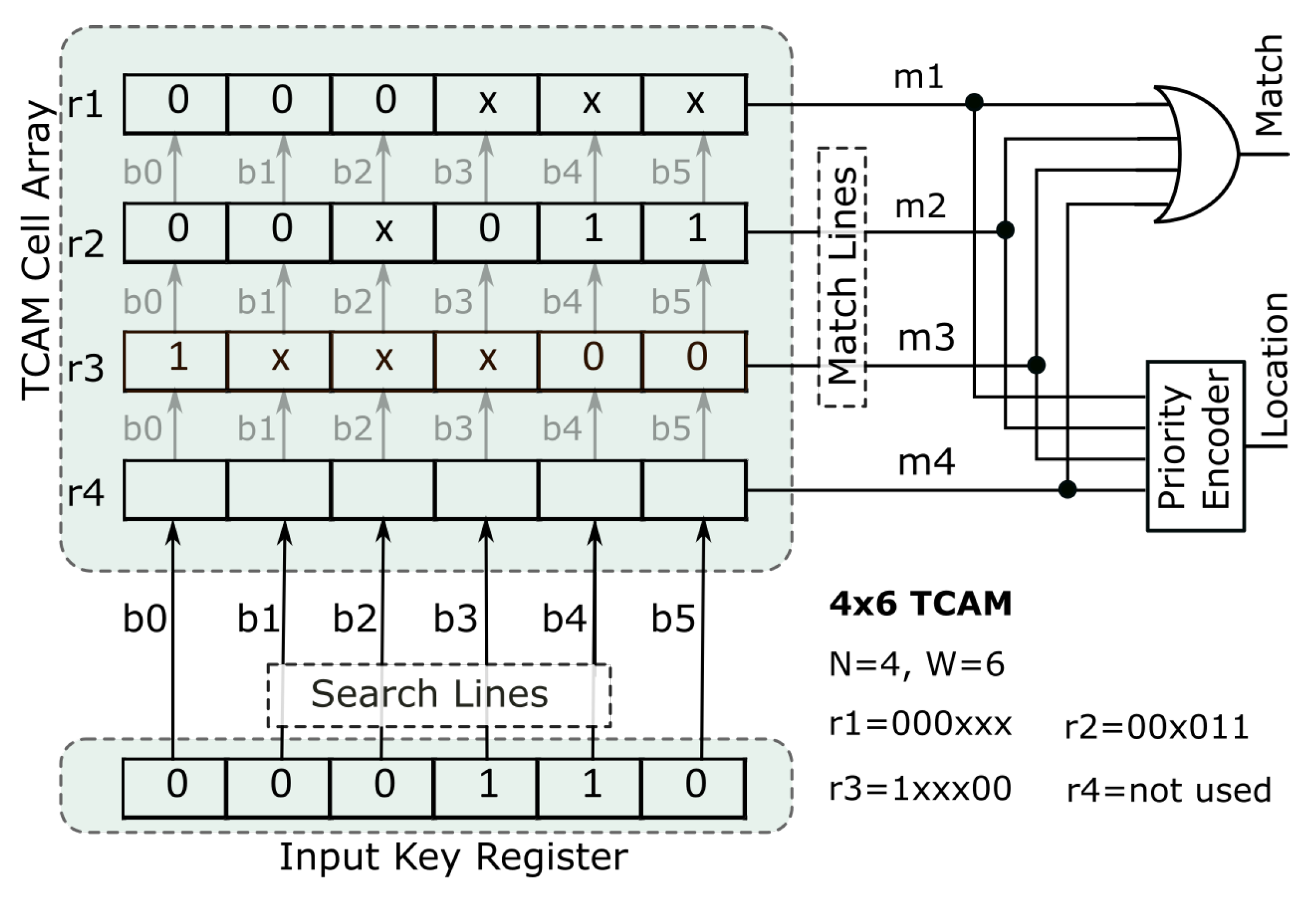
Traditionally, TCAMs have been implemented in ASICs. A conceptual architectural view of an ASIC-style 4 × 6 TCAM is depicted in Figure 1. This configuration supports four words or rules (i.e., N = 4) and each rule has six bits (i.e., W = 6). Such a TCAM is usually denoted by NxW TCAM. Each bit in the TCAM memory is stored in a TCAM cell which is implemented at transistor level [6]. The look-up operation for a TCAM starts with an input search key, that is received through the input search key register. Then, this key is searched in parallel in all TCAM stored words or rules. The matching rules generate a logic one value which are fed to a priority encoder and a reduction OR gate to generate a matching word address and match binary flag to indicate if a key has matched against a stored rule. The TCAM in Figure 1 implements four rules as shown in the figure. Note that each rule translates to a row in TCAM while rule size (or key size) corresponds to TCAM columns.
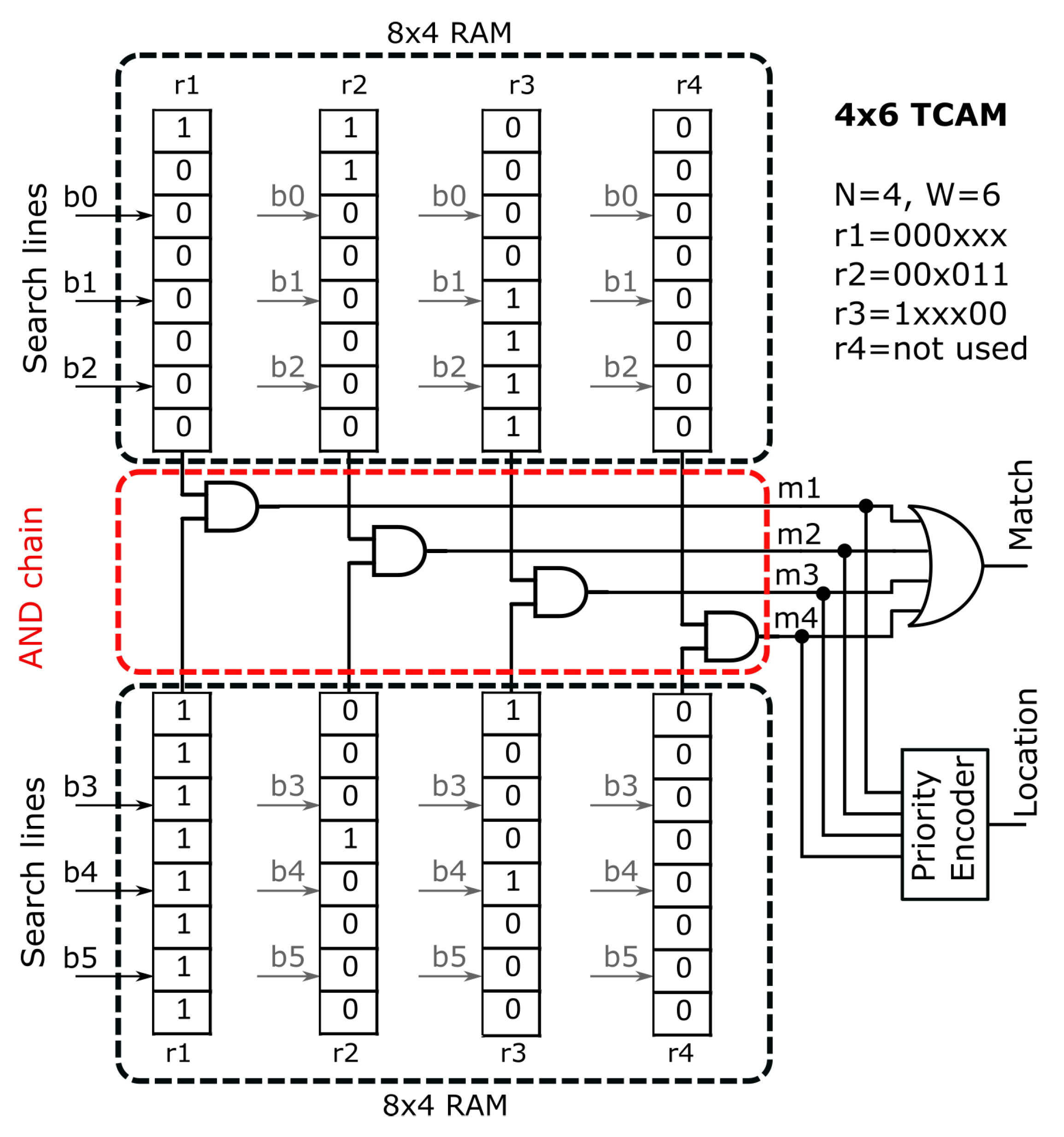
Now consider emulating the ASIC-style N × W TCAM using an SRAM on an FPGA. The dimension of RAM required for emulating an N × W TCAM is × N. With increasing size of W, the RAM depth will increase exponentially making RAM-based TCAM emulation impractical. In order to limit the exponential depth growth, the key W is split into several blocks, each sub-block indexes a different RAM memory [30]. For example, in Figure 2, the six bit key, W, is split in two two parts. The three upper bits index the upper × 4 RAM block while the lower three bits index the lower × 4 RAM block. Inside an individual 8 × 4 RAM block, each sub-rule is implemented through an 8 × 1 RAM. As an example, considering the mapping of r1 which is equal to 000xxx, in the upper 8 × 4 RAM block it is implemented by setting the RAM address 000 to 1, all other address locations are zero. While in the lower 8 × 4 RAM block, the xxx part of r1 is implemented by setting all address locations to 1. These two RAM blocks of r1 exits are combined with a chain of AND gates. Similarly, the same scheme is used for all the four rules. Therefore, each RAM block contains four smaller 8 × 1 RAMs generating four match line signals that are passed through the AND chains. Generally, the dimension of the match lines will be equal to N. The match lines are fed to a reduction-OR gate which takes as input an N bit vector and produces a single match output. Therefore, the dimension of AND gate depends upon the number of blocks into which a key is divided while the dimension of reduction-OR gate depends on the number of rules. There are two physical memories inside a Xilinx FPGA that can implement the TCAM emulation scheme outlined above that is, BRAMs or LUTRAMs. The cost of utilizing a BRAM-based TCAM is while that of LUTRAM based TCAM is that is, 56.8 SRAM bits per TCAM bit vs 6.4 SRAM bits per TCAM bit [30]. LUTRAM-based approaches have a lower cost per TCAM bit and support high-speed updates. Recent work in Reference [9] has achieved significant resource savings by mapping matching logic to unused architectural resources that is, carry-chains. However, the number of LUTRAMs (found in SLICEM) is quite small compared to traditional LUTs (found in SLICEL). Therefore, using LUTRAMs for TCAMs may not support large TCAM sizes. Similarly, using BRAMs for TCAMs may consume too many resources for large TCAM sizes leaving no spare resources for other modules of the application. Therefore, deciding on which option is best depends upon the context of design and the resource requirements [33]. Recent work in Reference [8] converts the problem of emulating TCAM on FPGAs from a sequential logic to pure combinational logic by leveraging LUT-level partial reconfiguration for TCAM updates. This enables the traditional LUTs located in SLICEL to be used for storing the rules in configuration memory. As lookup is a much more frequent operation in most TCAMs applications compared to the less frequent updates, the run-time reconfiguration overhead required for LUT-level rule updates is within bounds to support hundreds to thousands of rule updates per second with existing FPGAs. This is enough for many of the SDN application workloads. If the run-time partial reconfiguration integrates well with the overall system, it may be the best option as its RAM/TCAM bit ratio is same as LUTRAM and modern FPGAs have a huge number of LUTs. The following section presents the proposed methodology that improves the previously described TCAM emulation approaches.
4. Block and Partial Reconfiguration TCAM (BPR-TCAM)
This section presents the proposed BPR-TCAM approach by using in an unconventional manner the Xilinx FPGA’s slice resources, in particular, the LUTs and carry-chains. The proposed methodology terms the combination of LUTs and carry-chains in a slice as a “Block”. These Blocks are combined vertically and horizontally along the Configurable Logic Block (CLB) columns according to TCAM size. The vertical height depends upon the key bits while the horizontal width depends upon the number of rules in the TCAM implementation. In order to better understand the block structure and its usage, let us consider emulating a 2 × 66 TCAM. This can be optimally implemented by BPR-TCAM across 4 blocks. The first block in a CLB column is configured to implement a 2 × 20 TCAM, the middle two blocks are configured to implement 2 × 16 TCAMs while the last block in a column is configured to implement a 2 × 14 TCAM. The following paragraphs explain the first, middle and last blocks in full details.
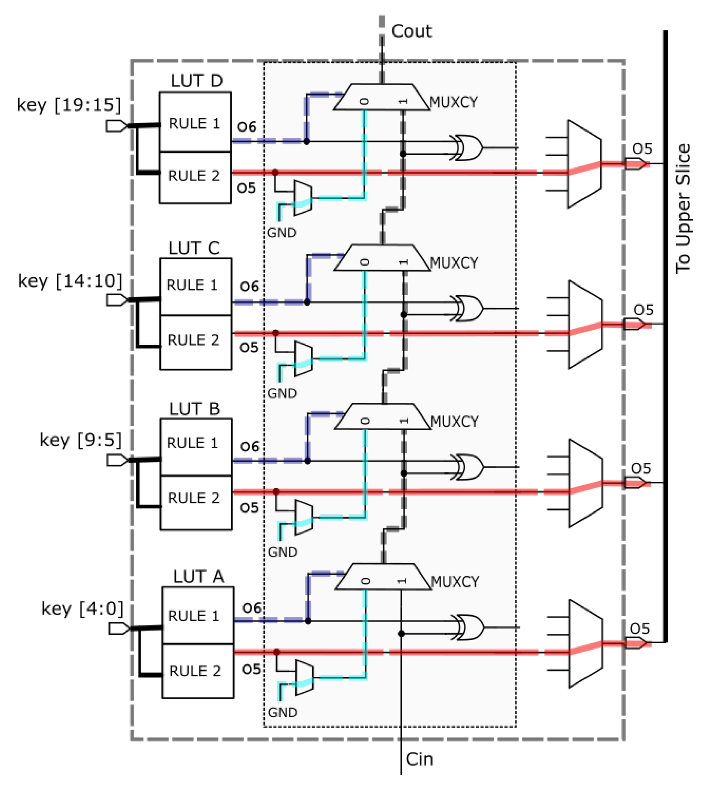
In order to better understand the details of the first block in a column, let us consider a TCAM with two rules and a key with bits that is, 2 × 20 TCAM emulated on a single FPGA slice illustrated in Figure 3. The LUTs are configured in dual-output mode (that is, 5 × 2 LUTs) where each LUT takes as input 5 bits of the key. Therefore, a total of 4 LUTs are required for 20 bit of the key housed entirely in a slice. However, it is worth mentioning that this arrangement supports storage memory requirements for two rules. One rule resides in the O5 LUTs and the second rule resides in O6 LUTs. Therefore, the entire slice is able to implement a Look Up Operation for a 2 × 20 TCAM. Interestingly, the AND-cascading for the matching logic for one of the implemented rules can also be realized using the built-in slice carry-chains as shown in Figure 3. Note that the O6 LUTs are AND-cascaded vertically along the carry-chain resources while the O5 LUTs producing four output signals are taken to the slice outputs. Therefore, a slice produces 5 outputs, a COUT output that represents the ANDed result of O6 LUTs and four O5 LUTs outputs. Note that the O5 outputs cannot be ANDed using the slice resources and require and additional LUT resources for ANDing operation.
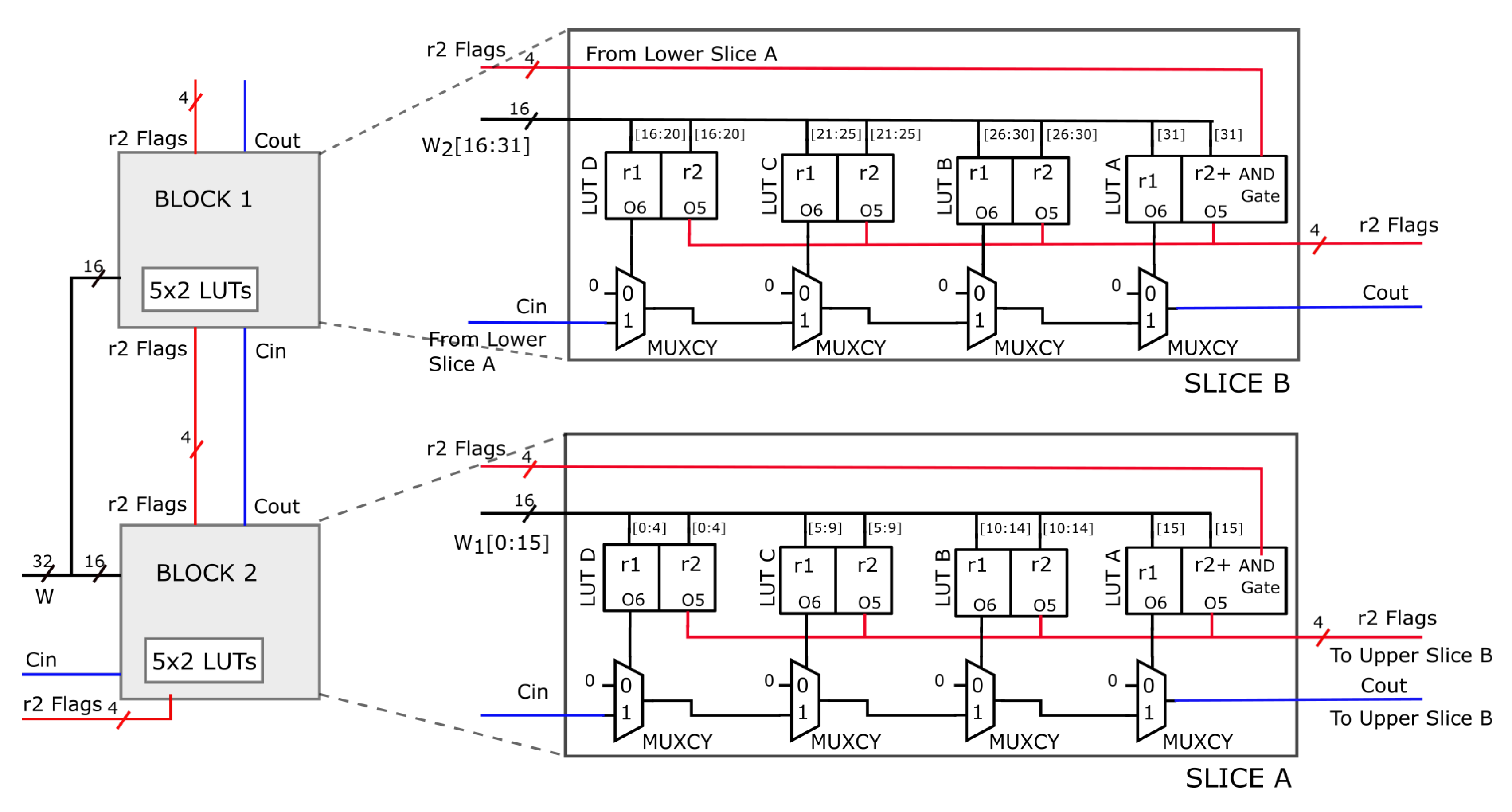
If the size of key is large, multiple slices can be stacked up to form a large AND-cascading along the carry-chain column. For example, consider a 2 × 32 TCAM depicted in Figure 4 utilizing two slices in 2 × 16 TCAM configuration mode implementing the middle slices of the proposed BPR-TCAM methodology. Figure 4 illustrates how two Blocks are combined for a 2 × 32 TCAM implementation. As before every 5 × 2 LUT implements two rules that is, “r1” through O6 and “r2” through O5. The r1’s are merged along the MUXCY element of carry-chains while the r2’s are merged with a LUT inside the next block. For example, consider LUT A of Slice A implementing Block 2, this LUT is configured to merge 4 O5s from the previous slice plus a single bit of key. Thus, this LUT implements a 4-input AND gate in O5, and a 1 × 1 TCAM in both O5 and O6. Such middle block forms the core of BPR-TCAM method and can be stacked along the CLB column for increasing key sizes.
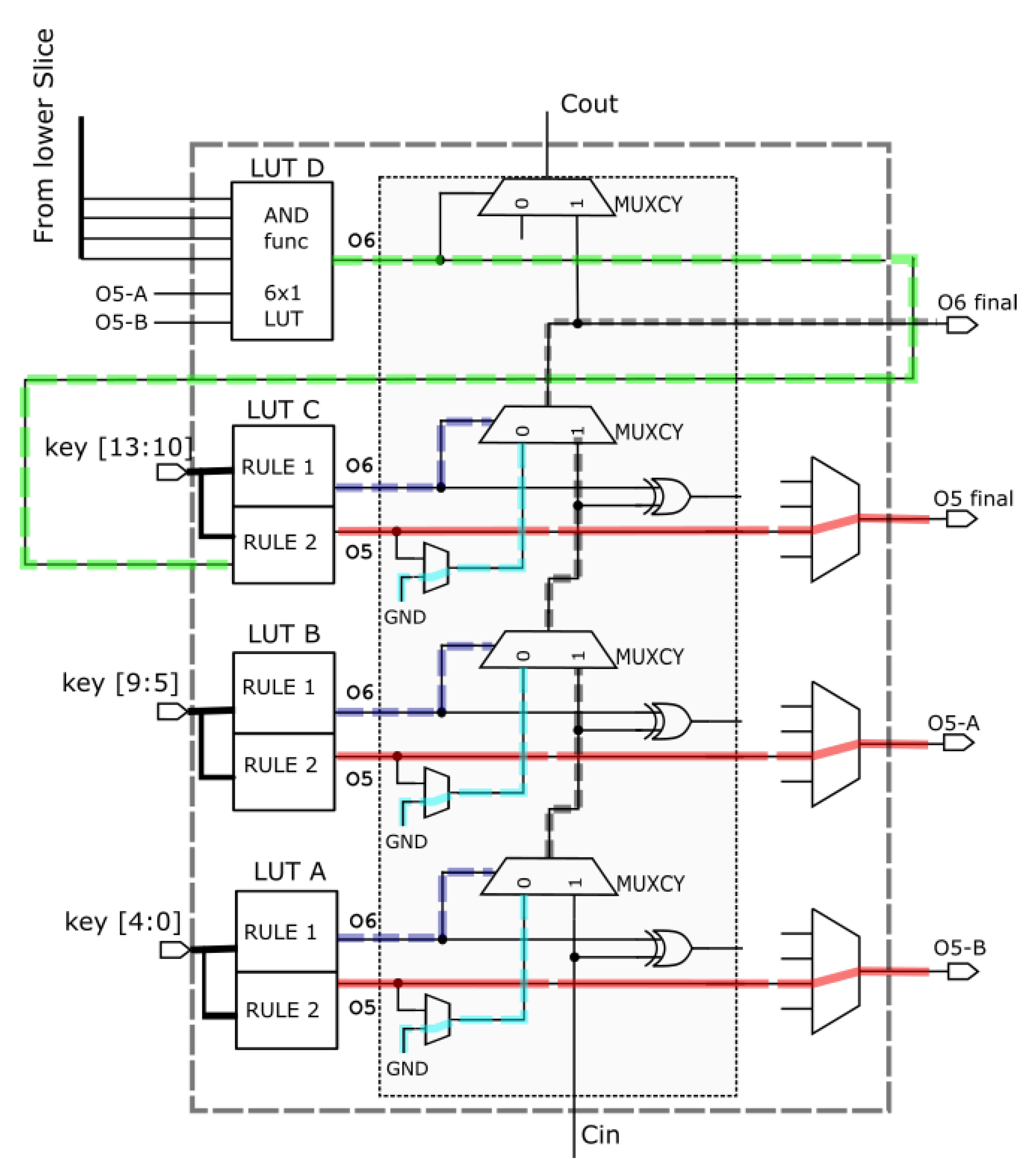
Finally, in order to understand the last block of a column, let us consider a 2 × 14 TCAM implementation illustrated in Figure 5. Although, LUT A and LUT B implement normal 5 × 2 LUTs of the BPR-TCAM, LUT C and LUT D are significantly different. This difference is introduced by the need to merge the O5s along the CLB column and to generate two bit match signals representing “r1” and “r2”. LUT D is configured to implement a 6 × 1 LUT, AND-merging 4 O5s from previous block and two O5s from the current block that is, LUT A and LUT B. Thus generating a single O5-merged result for “r2”. This merged r2 plus 4 key bits are combined in LUT C, configured in 5 × 2 mode to generate the final column-wise “r1” and “r2” match signals. These two match signals can then be connected to reduction-OR for final TCAM match signal.
In this way, the three different block types implement a 2 × 66 TCAM that is, first block implementing 2 × 20, two middle blocks implementing 2 × 32 and the last block implementing 2 × 14 configuration. If the AND-merging for the 2 × 66 TCAM is implemented with 5 × 2 LUTs as in the case of PR-TCAM but without carry-chains, it would incur an overhead of 3 6 × 1 LUTs per rule required for merging 14 5 × 2 LUTs. Thus for two rule per CLB column 6 LUTs are saved per four blocks of BPR-TCAM or a 1.5 LUTs saving per slice. This results in better FPGA slice utilization compared to existing FPGA TCAM approaches as will be seen in the evaluation presented in the next section.
5. Evaluation
This section presents the experimental results for different TCAM implementations on Xilinx Artix 7-series 28 nm XC7A100TCSG324-1, Xilinx Virtex-7 28 nm XC7V2000TFHG1761-2L and Xilinx Virtex-6 40 nm XC6VLX760 devices. The results are collected for 40, 80, 120 and 144 bits key sizes and 32, 64, 512 and 1024 number of rules and compared with existing work in literature. It should be noted that Xilinx ISE 14.7 design suite is used for collected results on Virtex-6 device while all other results are collected using Vivado HLx 16.3 design suite. It should be noted that the reported resource utilization and timing performance are reported post place-and-route phase of FPGA design flows. BPR-TCAM resource usage for the different key/rule sizes is given in Table 1. It is worth mentioning that the resources correspond to the BPR-TCAM blocks without the match reduction logic or priority encoders. The numbers can be related to the blocks used. For example, for a 32 × 40 TCAM, the first slice takes 20 key bits consuming 4 LUTs, the second takes 16 key bits plus 4 previous O5s consuming 4 LUTs and the last slice takes 4 key bits and 4 O5s from previous slice consuming 2 LUTs. Therefore, in total the 32 × 40 configuration, takes 10 LUTs per column and a total of 16 columns that is, 160 LUTs. Similarly, the slices count as 3 slices per column with a total of 16 columns making 48 slices in total. It can be seen that the resources tend to scale propotionally with the number of rules. Instead, the growth is lower with the key size. This is because large key sizes use more intermediate blocks that are more efficient.
BPR-TCAM delay on two different devices (i.e., Artix-7 denoted by Delay A7 and Virtex-7 denoted by V7) is also given in Table 1. It should be noted that the results for Artix-7 are collected with a speed grade of -1 while results for Virtex-7 correspond to speed grade −2. It should further be noted that the BPR-TCAM is implemented with registers in between different individual models, for example, registers are inserted between input and BPR-TCAM block and between BPR-TCAM block and Reduction-OR gate. This helps in isolating the delay results and confining the measurements only to the proposed BPR-TCAM structure. It can be noted that the delay for Virtex-7 increases by 1.72 ns as we move from 32 × 40 to 32 × 80 configuration and by 1.52 ns while moving from 32 × 80 to 32 × 120. Similarly, the delay increases by 2.61 ns as we move from 1024 × 40 to 1024 × 80 and by 1.84 ns while moving from 1024 × 80 to 1024 × 120. Therefore, the delay degradation while moving to larger configurations is moderate and does not double as the key size doubles. Although, the reported delay for Artix-7 is higher compared to Virtex-7 due to difference in speed grades, a similar trend can be observed when the key size increases for a constant rule size. Thus, the delay of BPR-TCAM scales well with size of TCAM.
Table 2 compares existing works with the proposed BPR-TCAM in terms of resource usage and speed. It can be seen that BPR-TCAM-I is 54% and 41% efficient than DURE-I and PR-TCAM respectively in slice resource utilization. However, BPR-TCAM-I is 52.8% worse in speed comparison to DURE-I. The reason being that DURE is based on LUTRAMs which are clocked-sequential elements compared LUTs which are combinational logic elements. It can be noted that BPR-TCAM-I is 62.5% better is speed performance than PR-TCAM because of pipelined registers.
Table 3 gives a comparison of existing FPGA TACMs and BPR-TCAM irrespective of the FPGA device technology. This has been achieved by utilizing normalization according to well-know equations from the literature. For example, Equation (1) gives the normalized slices and is useful when a design uses BRAMs. This actually converts the number of utilized BRAMs into corresponding LUT resources and calculates the resultant slices.
Similarly, to take care of different technology nodes, Equation (2) maps the results from FPGAs in any technology into 40 nm equivalent ones since most of the existing literature was implemented in 40 nm technology FPGAs.
Also, throughput is given by Equation (3) which represents the capacity of data transfer to and from the TCAM. It can be noted from Table 3 that BPR-TCAM-I has a throughput of 8.77 Gbit/sec which outperforms all of the existing works except DURE-I which has a throughput of 12.06 Gbit/sec.
A single metric to compare different TCAM implementations is Performance Per Area (PA) given by Equation (4).
The PA has been defined in [9] as a metric that captures the performance versus the resource usage regardless of the implementation approach used. This is done by normalizing the speed and the resources (also shown in the table) and assigning a cost to each normalized resource type so that an aggregated normalized resource usage can be computed. It can be observed that BPR-TCAM outperforms all the existing implementations in terms of PA. The main contributing factor to this gain is a lower resource usage of BPR-TCAM that compensates its slightly worse delay compared to some of the existing schemes. For example, consider DURE 512 × 36 configuration and BPR-TCAM 512 × 40 configuration, it can be observed that although DURE offers a higher clock rate, due to significant resource savings, BPR-TCAM has a higher PA 5.85 compared to 3.7 for DURE. Similarly, comparing PR-TCAM 512 × 40 and BPR-TCAM 512 × 40, it can be observed that BPR-TCAM has a PA of 5.85 compared to 1.08 of PR-TCAM. These results show that the proposed TCAM implementation outperforms existing work by a considerable margin.
6. Conclusions and Future Work
In this paper, BPR-TCAM, an efficient methodology is presented for mapping the logic needed to emulate TCAMs to the FPGA slice structure. This is achieved by an unconventional utilization of slice carry-chain resources for implementing the AND-cascading required for matching logic. Combined with the dual-output LUTs and the use of partial reconfiguration, carry-chain based AND-cascading results in more than a single LUT saving per slice, thereby, significantly reducing the matching logic overhead.The evaluation and comparison with existing implementations show that the proposed BPR-TCAM can significantly reduce the cost of emulating TCAMs on FPGAs. In particular, savings of more than 30% in the number of normalized slices required to implement a given TCAM were achieved compared to existing schemes.
Author Contributions
A.U., A.Z. and P.R. contributed to the design of the proposed TCAM architecture. A.Z., N.A.K., W.A. and A.R. contributed to the implementation of the emulated TCAM and simulations. A.U., A.Z., A.R. and P.R. participated in the writing and revision of the paper. All authors contributed to the analysis of the results and comparisons with previous schemes. All authors have read and agreed to the published version of the manuscript
Funding
Pedro Reviriego would like to acknowledge the support of the TEXEO project TEC2016-80339-R funded by the Spanish Ministry of Economy and Competitivity and of the Madrid Community research project TAPIR-CM grant no. P2018/TCS-4496.
Conflicts of Interest
The authors declare no conflicts of interest.
References
- Zilberman, N.; Audzevich, Y.; Covington, G.A.; Moore, A.W. NetFPGA SUME: Toward 100 Gbps as Research Commodity. IEEE Micro 2014, 34, 32–41. [Google Scholar] [CrossRef]
- Xilinx. SDNet Packet Processor User Guide; UG1012 (v2018.1); Xilinx: San Jose, CA, USA, 2018. [Google Scholar]
- Reviriego, P.; Pontarelli, S.; Levy, G. CuCoTrack: Cuckoo filter based connection tracking. Inf. Process. Lett. 2019, 147, 55–60. [Google Scholar] [CrossRef] [Green Version]
- Sundstron, M.; Larzon, L. Åke High-performance longest prefix matching supporting high-speed incremental updates and guaranteed compression. In Proceedings of the 24th Annual Joint Conference of the IEEE Computer and Communications Societies, Miami, FL, USA, 13–17 March 2005; Volume 3, pp. 1641–1652. [Google Scholar]
- Yu, F.; Katz, R.; Lakshman, T. Efficient Multimatch Packet Classification and Lookup with TCAM. IEEE Micro 2005, 25, 50–59. [Google Scholar]
- Pagiamtzis, K.; Sheikholeslami, A. Content-Addressable Memory (CAM) Circuits and Architectures: A Tutorial and Survey. IEEE J. Solid-state Circuits 2006, 41, 712–727. [Google Scholar] [CrossRef]
- Bosshart, P.; Gibb, G.; Kim, S.H.; Varghese, G.; McKeown, N.; Izzard, M.; Mujica, F.; Horowitz, M. Forwarding metamorphosis: Fast programmable match-action processing in hardware for SDN. In Proceedings of the Conference of the ACM Special Interest Group on Data Communication (SIGCOMM ’13), Hong Kong, China, 12–16 August 2013. [Google Scholar]
- Reviriego, P.; Ullah, A.; Pontarelli, S. PR-TCAM: Efficient TCAM Emulation on Xilinx FPGAs Using Partial Reconfiguration. IEEE Trans. Very Large Scale Integr. Syst. 2019, 27, 1952–1956. [Google Scholar] [CrossRef]
- Ullah, I.; Ullah, Z.; Afzaal, U.; Lee, J.-A. DURE: An Energy- and Resource-Efficient TCAM Architecture for FPGAs With Dynamic Updates. IEEE Trans. Very Large Scale Integr. Syst. 2019, 27, 1–10. [Google Scholar] [CrossRef]
- Yu, W.; Sivakumar, S.; Pao, D. Pseudo-TCAM: SRAM-Based Architecture for Packet Classification in One Memory Access. IEEE Netw. Lett. 2019, 1, 89–92. [Google Scholar] [CrossRef]
- Lim, H.; Lee, S.; Swartzlander, E.E. A new hierarchical packet classification algorithm. Comput. Netw. 2012, 56, 3010–3022. [Google Scholar] [CrossRef]
- Jiang, W.; Prasanna, V.K. Scalable Packet Classification on FPGA. IEEE Trans. Very Large Scale Integr. Syst. 2011, 20, 1668–1680. [Google Scholar] [CrossRef]
- Kennedy, A.; Wang, X. Ultra-High Throughput Low-Power Packet Classification. IEEE Trans. Very Large Scale Integr. Syst. 2013, 22, 286–299. [Google Scholar] [CrossRef] [Green Version]
- Pao, D.; Lu, Z.; Pao, C.W.D. A multi-pipeline architecture for high-speed packet classification. Comput. Commun. 2014, 54, 84–96. [Google Scholar] [CrossRef]
- Chang, Y.-K.; Chen, H.-C. Fast Packet Classification using Recursive Endpoint-Cutting and Bucket Compression on FPGA. Comput. J. 2018, 62, 198–214. [Google Scholar] [CrossRef]
- Irfan, M.; Ullah, Z. G-AETCAM: Gate-Based Area-Efficient Ternary Content-Addressable Memory on FPGA. IEEE Access 2017, 5, 20785–20790. [Google Scholar] [CrossRef]
- Ullah, Z. LH-CAM: Logic-based Higher Performance Binary CAM Architecture on FPGA. IEEE Embed. Syst. Lett. 2017, 9, 1. [Google Scholar] [CrossRef]
- Irfan, M.; Ahmad, A. Impact of Initialization on Gate-Based Area Efficient Ternary Content-Addressable Memory. In Proceedings of the 2018 International Conference on Computing, Electronics & Communications Engineering (iCCECE), Southend, UK, 16–17 August 2018; pp. 328–332. [Google Scholar]
- Mahmood, H.; Ullah, Z.; Mujahid, O.; Ullah, I.; Hafeez, A. Beyond the Limits of Typical Strategies: Resources Efficient FPGA-Based TCAM. IEEE Embed. Syst. Lett. 2019, 11, 89–92. [Google Scholar] [CrossRef]
- Somasundaram, M. Circuits to Generate a Sequential Index for an Input Number in a Pre-Defined List of Numbers. U.S. Patent 7 155 563 B1, 26 December 2006. [Google Scholar]
- Ullah, Z.; IlGon, K.; Baeg, S. Hybrid Partitioned SRAM-Based Ternary Content Addressable Memory. IEEE Trans. Circuits Syst. I: Regul. Pap. 2012, 59, 2969–2979. [Google Scholar] [CrossRef]
- Ullah, Z.; Jaiswal, M.K.; Cheung, C.C.R. Z-TCAM: An SRAM-based Architecture for TCAM. IEEE Trans. Very Large Scale Integr. Syst. 2014, 23, 402–406. [Google Scholar] [CrossRef]
- Ullah, Z.; Jaiswal, M.K.; Cheung, R.C.C.; Cheung, C.C.R. E-TCAM: An Efficient SRAM-Based Architecture for TCAM. Circuits, Syst. Signal Process. 2014, 33, 3123–3144. [Google Scholar] [CrossRef]
- Ullah, Z.; Jaiswal, M.K.; Cheung, R.C.; So, H.K.; Cheung, C.C.R. UE-TCAM: An ultra efficient SRAM-based TCAM. In Proceedings of the TENCON 2015–2015 IEEE Region 10 Conference, Macao, China, 1–4 November 2015; Institute of Electrical and Electronics Engineers (IEEE); pp. 1–6. [Google Scholar]
- Ahmed, A.; Park, K.; Baeg, S. Resource-Efficient SRAM-based Ternary Content Addressable Memory. IEEE Trans. Very Large Scale Integr. Syst. 2016, 25, 1–5. [Google Scholar] [CrossRef]
- Ullah, I.; Ullah, Z.; Lee, J.-A.; Ullaha, Z. Efficient TCAM Design Based on Multipumping-Enabled Multiported SRAM on FPGA. IEEE Access 2018, 6, 19940–19947. [Google Scholar] [CrossRef]
- Syed, F.; Ullah, Z.; Jaiswal, M.K. Fast Content Updating Algorithm for an SRAM-Based TCAM on FPGA. IEEE Embed. Syst. Lett. 2017, 10, 73–76. [Google Scholar] [CrossRef]
- Ullah, I.; Ullah, Z.; Lee, J.-A. EE-TCAM: An Energy-Efficient SRAM-Based TCAM on FPGA. Electronics 2018, 7, 186. [Google Scholar] [CrossRef] [Green Version]
- Reviriego, P.; Pontarelli, S.; Ullah, A.; Zahir, A.; Bianchi, G. Multiple Hash Matching Units (MHMU): An Algorithmic Ternary Content Addressable Memory Design for Field Programmable Gate Arrays. In Proceedings of the 2018 IEEE 19th International Conference on High Performance Switching and Routing (HPSR), Bucharest, Romania, 18–20 June 2018; pp. 1–6. [Google Scholar]
- Jiang, W. Scalable Ternary Content Addressable Memory implementation using FPGAs. Arch. Netw. Commun. Syst. 2013, 71–82. [Google Scholar]
- Qian, Z.; Margala, M. Low power RAM-based hierarchical CAM on FPGA. In Proceedings of the 2014 International Conference on ReConFigurable Computing and FPGAs (ReConFig14), Cancun, Mexico, 8–10 December 2014; pp. 1–4. [Google Scholar]
- Locke, K. Parameterizable Content-Addressable Memory; Xilinx: San Jose, CA, USA, 2011. [Google Scholar]
- Xilinx. Ternary Content Addressable Memory (TCAM) Search IP for SDNet. In SmartCORE IP Product Guide; PG190 (v1.0); Xilinx: San Jose, CA, USA, 2017. [Google Scholar]
- Maidee, P. Multiplexer-Based Ternary Content Addressable Memory. U.S. Patent 9653165, 16 May 2017. [Google Scholar]
Figure 1.
A conceptual view of a 4 × 6 ASIC-style Ternary Content Addressable Memory (TCAM).

Figure 2.
Example of a 4 × 6 TCAM emulated using two 8 × 4 SRAMs.

Figure 3.
Mapping of a 2 × 20 TCAM to four 5 × 2 LUTs in a first slice.

Figure 4.
Architecture of Proposed method for a 2 × 32 TCAM.

Figure 5.
Mapping of a 2 × 14 TCAM to four 5 × 2 LUTs in a last slice.


Table 1.
Resource and Delay (in nanoseconds) Results for BPR-TCAM on Artix-7 XC7A100T and Virtex-7 XC7V2000TFHG1761-2L.
Table 1.
Resource and Delay (in nanoseconds) Results for BPR-TCAM on Artix-7 XC7A100T and Virtex-7 XC7V2000TFHG1761-2L.
| KEY | PARAMETER | RULES | |||
|---|---|---|---|---|---|
| 32 | 64 | 512 | 1024 | ||
| 40 | LUTS | 160 | 320 | 2560 | 5120 |
| FFs | 145 | 209 | 1105 | 2129 | |
| SLICES | 48 | 96 | 768 | 1536 | |
| DELAY-V7 | 2.52 | 2.61 | 2.78 | 3.21 | |
| DELAY-A7 | 4.70 | 5.25 | 5.38 | 6.00 | |
| 80 | LUTS | 320 | 640 | 5120 | 10,240 |
| FFs | 225 | 289 | 1185 | 2209 | |
| SLICES | 80 | 160 | 1280 | 2560 | |
| DELAY-V7 | 4.24 | 4.79 | 5.32 | 5.82 | |
| DELAY-A7 | 8.10 | 8.67 | 10.16 | 10.36 | |
| 120 | LUTS | 480 | 960 | 7680 | 15,360 |
| FFs | 305 | 369 | 1265 | 2289 | |
| SLICES | 128 | 256 | 2048 | 4096 | |
| DELAY-V7 | 5.76 | 6.16 | 6.82 | 7.66 | |
| DELAY-A7 | 11.40 | 12.18 | 13.53 | 14.98 | |
Table 2.
Resource and Speed (MHz) comparison of BPR-TCAM with state-of-the-art TCAMs.
| Architecture | Device | Size | LUTRAMs | LUTs | FFs | BRAMs | Slices | Speed |
|---|---|---|---|---|---|---|---|---|
| HP-TCAM [21] | XC6VLX760 | 512 × 36 | 0 | 6546 | 2670 | 56 | 1637 | 118 |
| Z-TCAM [22] | XC6VLX760 | 512 × 36 | 0 | 4462 | 2178 | 40 | 1116 | 159 |
| UE-TCAM [24] | XC6VLX760 | 512 × 36 | 0 | 3652 | 1758 | 32 | 913 | 202 |
| Syed [27] | XC6VLX760 | 512 × 36 | 0 | 3013 | 552 | 32 | 754 | 101 |
| DURE-I [9] | XC6VLX760 | 512 × 36 | 4096 | 1605 | 1174 | 0 | 1668 | 335 |
| PR-TCAM [8] | XC7A100T | 512 × 40 | 0 | 3574 | 0 | 0 | 1085 | 82 |
| BPR-TCAM I | XC6VLX760 | 512 × 40 | 0 | 2560 | 793 | 0 | 768 | 219.2 |
| Xilinx [33] | XC7V2000T | 512 × 128 | 8875 | 27,559 | 35,068 | 3 | 12,011 | 171 |
| DURE-II [9] | XC6VLX760 | 1024 × 144 | 32,768 | 3039 | 2700 | 0 | 9654 | 175 |
| BPR-TCAM II | XC6VLX760 | 1024 × 144 | 0 | 18,432 | 3029 | 0 | 4608 | 111.49 |
| Jiang [30] | XC7V2000T | 1024 × 150 | 20,480 | 61,624 | 37,556 | 0 | 20,526 | 199 |
Table 3.
Throughput (Throughput in Gbit/s) and Performance Per Area (PA in (Mbit/s)/Slice) comparison of BPR-TCAM with state-of-the-art TCAMs.
Table 3.
Throughput (Throughput in Gbit/s) and Performance Per Area (PA in (Mbit/s)/Slice) comparison of BPR-TCAM with state-of-the-art TCAMs.
| Architecture | Device | Size | N.Slices | N. Speed | Throughput | PA |
|---|---|---|---|---|---|---|
| HP-TCAM [21] | XC6VLX760 | 512 × 36 | 2981 | 118 | 4.25 | 0.73 |
| Z-TCAM [22] | XC6VLX760 | 512 × 36 | 2076 | 159 | 5.72 | 1.41 |
| UE-TCAM [24] | XC6VLX760 | 512 × 36 | 1681 | 202 | 7.26 | 2.21 |
| Syed [27] | XC6VLX760 | 512 × 36 | 1522 | 101 | 3.64 | 1.22 |
| DURE-I [9] | XC6VLX760 | 512 × 36 | 1668 | 335 | 12.06 | 3.7 |
| PR-TCAM [8] | XC7A100T | 512 × 40 | 1085 | 57.4 | 2.3 | 1.08 |
| BPR-TCAM I | XC6VLX760 | 512 × 40 | 768 | 219.2 | 8.77 | 5.85 |
| Xilinx [33] | XC7V2000T | 512 × 128 | 12,083 | 120 | 15.36 | 0.65 |
| DURE-II [9] | XC6VLX760 | 1024 × 144 | 9654 | 175 | 25.2 | 2.67 |
| BPR-TCAM II | XC6VLX760 | 1024 × 144 | 4608 | 111.49 | 16.05 | 3.57 |
| Jiang [30] | XC7V2000T | 1024 × 150 | 20,526 | 139 | 20.9 | 1.04 |
© 2020 by the authors. Licensee MDPI, Basel, Switzerland. This article is an open access article distributed under the terms and conditions of the Creative Commons Attribution (CC BY) license (http://creativecommons.org/licenses/by/4.0/).
Share and Cite
MDPI and ACS Style
Ullah, A.; Zahir, A.; Khan, N.A.; Ahmad, W.; Ramos, A.; Reviriego, P. BPR-TCAM—Block and Partial Reconfiguration based TCAM on Xilinx FPGAs. Electronics 2020, 9, 353. https://doi.org/10.3390/electronics9020353
AMA Style
Ullah A, Zahir A, Khan NA, Ahmad W, Ramos A, Reviriego P. BPR-TCAM—Block and Partial Reconfiguration based TCAM on Xilinx FPGAs. Electronics. 2020; 9(2):353. https://doi.org/10.3390/electronics9020353
Chicago/Turabian StyleUllah, Anees, Ali Zahir, Noaman A. Khan, Waleed Ahmad, Alexis Ramos, and Pedro Reviriego. 2020. "BPR-TCAM—Block and Partial Reconfiguration based TCAM on Xilinx FPGAs" Electronics 9, no. 2: 353. https://doi.org/10.3390/electronics9020353
Note that from the first issue of 2016, this journal uses article numbers instead of page numbers. See further details here.