Article

CMOS Analog Filter Design for Very High Frequency Applications

by
Luis Abraham Sánchez-Gaspariano
1,*,
Carlos Muñiz-Montero
2,
Jesús Manuel Muñoz-Pacheco
1,
Carlos Sánchez-López
3,
Luz del Carmen Gómez-Pavón
1,
Arnulfo Luis-Ramos
1 and
Alejandro Israel Bautista-Castillo
2
1
Facultad de Ciencias de la Electrónica, Benemérita Universidad Autónoma de Puebla, Ciudad Universitaria, 18 Sur y Avenida San Claudio, San Manuel, Puebla 72000, Mexico
2
Ingeniería en Electrónica y Telecomunicaciones, Universidad Politécnica de Puebla, Tercer Carril del Ejido Serrano S/N, San Mateo Cuanalá, Juan C. Bonilla, Puebla 72000, Mexico
3
Facultad de Ciencias Básicas, Ingeniería y Tecnología, Universidad Autónoma de Tlaxcala, Apizaquito Km. 1.5, Apizaco, Tlaxcala 90300, Mexico
*
Author to whom correspondence should be addressed.
Electronics 2020, 9(2), 362; https://doi.org/10.3390/electronics9020362
Submission received: 27 January 2020 / Revised: 7 February 2020 / Accepted: 7 February 2020 / Published: 21 February 2020
(This article belongs to the Section Circuit and Signal Processing)

Abstract

:
A design strategy for the synthesis of high-selectivity/low-order analog filters in Complementary Metal-Oxide-Semiconductor (CMOS) technology for very high frequency (VHF) applications is presented. The methodology for the reconstitution of a given transfer function by means of Signal Flow Graphs (SFG) manipulation in canonical form is proposed leading to a fully differential g m -C biquad filter. As a practical example, the design of a notch filter intended to suppress interferers in the lower sideband (400 MHz) of the Medical Implant Communication Service (MICS), in single-poly, 6-metal layers; Mixed-Signal/RF 0.18 µm CMOS technology is realized. To compare the performance of the proposal with some other solution, the design of a 7th order elliptic notch filter based on Frequency Dependent Negative Resistors (FDNRs) was also accomplished. The attained simulation results prove that the proposal is competitive compared to the FDNR solution and some other state-of-the-art filters reported in the literature. The most salient features of the proposed notch biquad include: the selectivity, whose value is comparable to that of a 7th order elliptic approach and some other 3rd order filters; a high-frequency operation without resonators; linearity, with a +15 dBm I I P 3 ; a reduced form factor with a total occupied area of 0.004282 mm2 and mostly a low design complexity.

1. Introduction

The most remarkable development in filter theory dates from the early decades of the last century [1,2,3]. As signal processing in electronics engineering became more relevant, this branch of knowledge evolved rendering filter structures capable of accomplishing functions whose theoretical background is rigorous and elegant at the same time. Examples of such filter architectures are digital filters. Digital filtering is employed in a vast cluster of applications such as voice encoding/decoding [4], image processing [5], control systems [6], data compression [7], and telecommunications [8], to name a few. While many filtering tasks use digital signal processing, continuous-time filters are still important. Some of the assignments that analog filters can carry on include: frequency duplexing in radar and radio communication systems [9]; impedance matching in power amplifiers [10]; upper-sideband and lower-sideband suppression in upconversion and downconversion mixers [11], respectively; anti-aliasing in data converters [12], among others. If difficult trade-offs in their implementation did not limit their usefulness, continuous time filters would be employed in many more applications. Unfortunately, a confined number of analog filters are realized in active form because they have proved to be the most reliable and versatile in terms of circuit realization, sensitivity, and mathematical complexity. Such is the case of Transconductance-Capacitance (gm-C) filters [13].
There are several major advantages to using CMOS gm-C filters as compared to the Operational Amplifier (Op-Amp) RC approximations, for instance, their higher frequency ranges with simple tuning [14], and the fact that gm-C and digital signal processing circuits can be fabricated on the same chip, which reduces the cost and size at the same time that increases the reliability of the hardware [13]. On the other hand, some drawbacks related to the use of CMOS gm-C filters also poke out: their parasitic capacitances are often considerable and require to be taken into account in advance in the design procedure [13]; at high frequencies, the value of the transconductance varies with frequency [15]; their useful signal dynamic range is rather low due to the nonlinearity inherent to the MOS transistors [14]. Despite those disadvantages, huge efforts have been made in order to achieve gm-C structures with a salient functionality at very high frequencies [16,17], and with improved linearity [18,19].
However, to enhance the selectivity, which is the ability to pass a set of signals within a bandwidth while rejecting the waveforms outside the band pass, it is a common practice to increase the order (number of transfer-function poles) of the filter. Increasing filter order adds complexity, chip area, and power consumption. Furthermore, high selectivity filtering also requires pole pairs to be complex conjugate with some some of them having high quality factor (Q) [15]. In this paper, the methodology to synthesize Q-enhanced g m -C biquad filters based on the use of Signal-Flow-Graphs (SFGs) is presented. A procedure to formulate the SFGs from any linear filter transfer function and then, from this point, to blend g m -C biquad filters with improved selectivity by SFG manipulation is described in Section 2. Section 3 presents a design example of a biquad RF notch filter for blocker with Q = 20 and f 0 = 400 MHz in a single-poly, 6-metal layers, Mixed-Signal/RF 0.18 µm CMOS technology, for being employed in the Medical Implant Communication Service (MICS). The obtained simulation results are reported in Section 4. Finally, the conclusions are drawn in Section 5.

2. Q Enhanced gm-C Filters

The concept of Q is used in many different contexts, and its fundamental definition relates total stored energy to energy loss [20]. On the scene of filter theory, it refers to the ability to pass a set of signals within a bandwidth while rejecting the waveforms outside the band pass. A common manner for increasing the Q of an integrated filter without augmenting the filter order is by means of tank circuits. Such approach presents the advantage of allowing the implementation of filters at very high frequencies [15]. However, the main drawback of active filters based on tank resonator circuits is the fact that the range at which the cutoff frequency can be tuned is rather narrow. Moreover, the implementation of high quality passive devices such as inductors in a Silicon technology is rather complicated [20].
On the other hand, the proposed procedure herein consists of manipulating the SFGs of a biquad gm-C filter in order to modify, merely, the first order coefficient from the denominator polynomial of its transfer function and hence to improve the selectivity of the circuit.

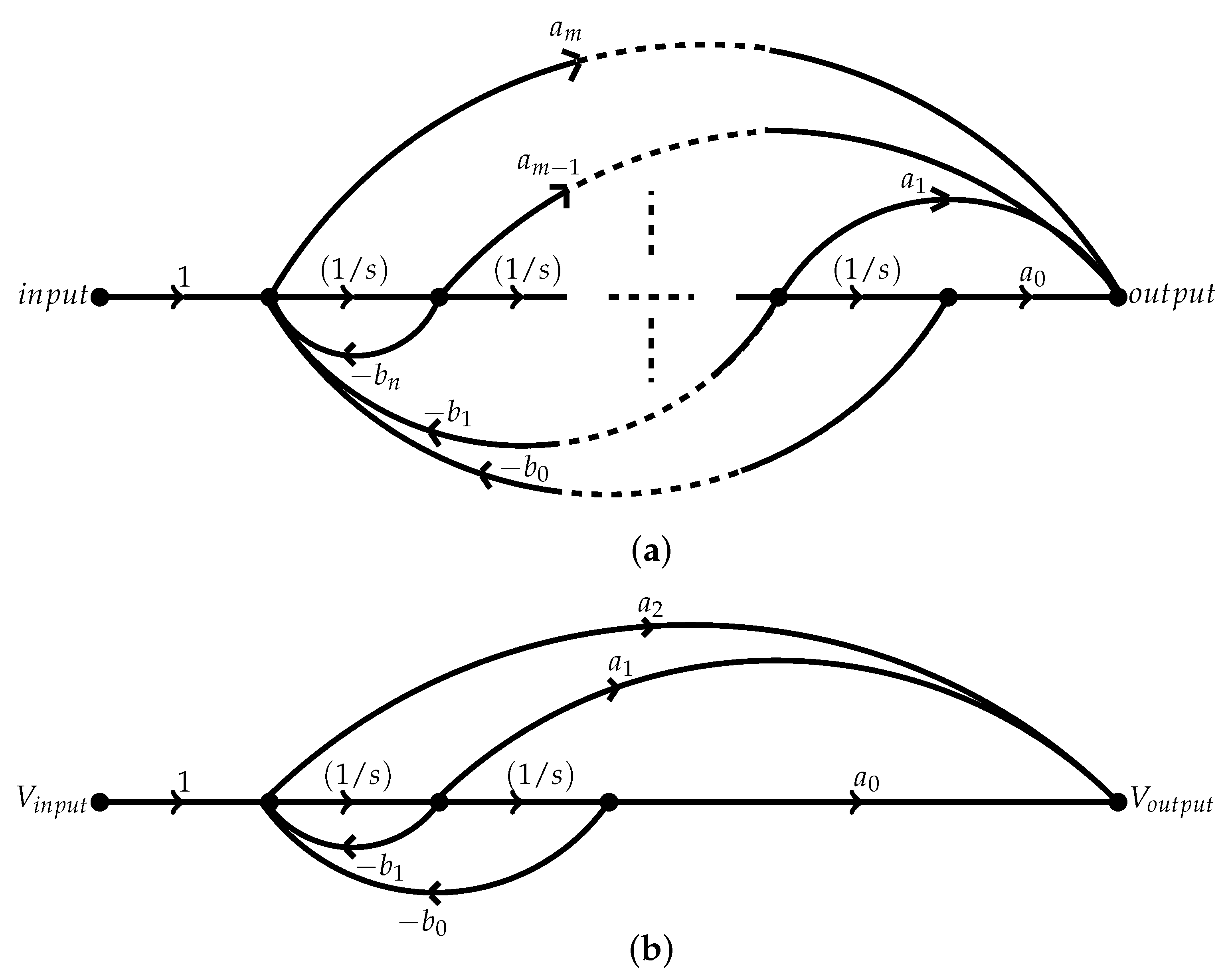
2.1. Formulation of the SFG from a Filter Transfer Function

Typically, when synthesizing active filters by means of SFGs, the starting point is to build up the graph of a passive ladder network, commonly a filter, and then to proceed with an active leapfrog realization [21]. Another way of using the SFGs approximation is to draw the graph directly from the transfer function of the filter [22].
Let the transfer function of a filter be (The reason because the form ( 1 / s ) is employed instead of s in (1) is that integrators are preferred over differentiators in a practical circuit realization.) [22]
T ( s ) = a m 1 s n m + a m 1 1 s n m + 1 + + a 1 1 s n 1 + a 0 1 s n 1 + b n 1 1 s + + b 1 1 s n 1 + b 0 1 s n
where m , n Z satisfying m n , and a i , b j 1 , are the i-th and j-th coefficients of the numerator and denominator polynomials, respectively.
It can be proved by means of the gain formula of Mason that the SFG in controllable canonical form of Figure 1a describes the transfer function expressed in (1). The reason of using such graph is that it has two important features: all loops in the graph touch each other and every forward pathway from the input node to the output node touches all loops. These characteristics allow for enunciating the gain formula of Mason as [22]
T ( s ) = P k 1 L n
where P k is the k-th forward path weight, L n is the n-th loop weight, and summations are all over the direct pathways as well as the loops. Thus, L 1 = b n 1 s , L 2 = b n 2 s 2 , , L n = b 0 s n , whereas P 1 = a m , P 2 = a m 1 s , , P n = a 0 s n .
The convenience of the graph representation in the form depicted in Figure 1a lies in its feasibility for adjusting a specific coefficient, either (or even both) from the numerator or denominator polynomials of T ( s ) by changing the value of the corresponding forward/backward pathway in a given loop. This is demonstrated in the successive.

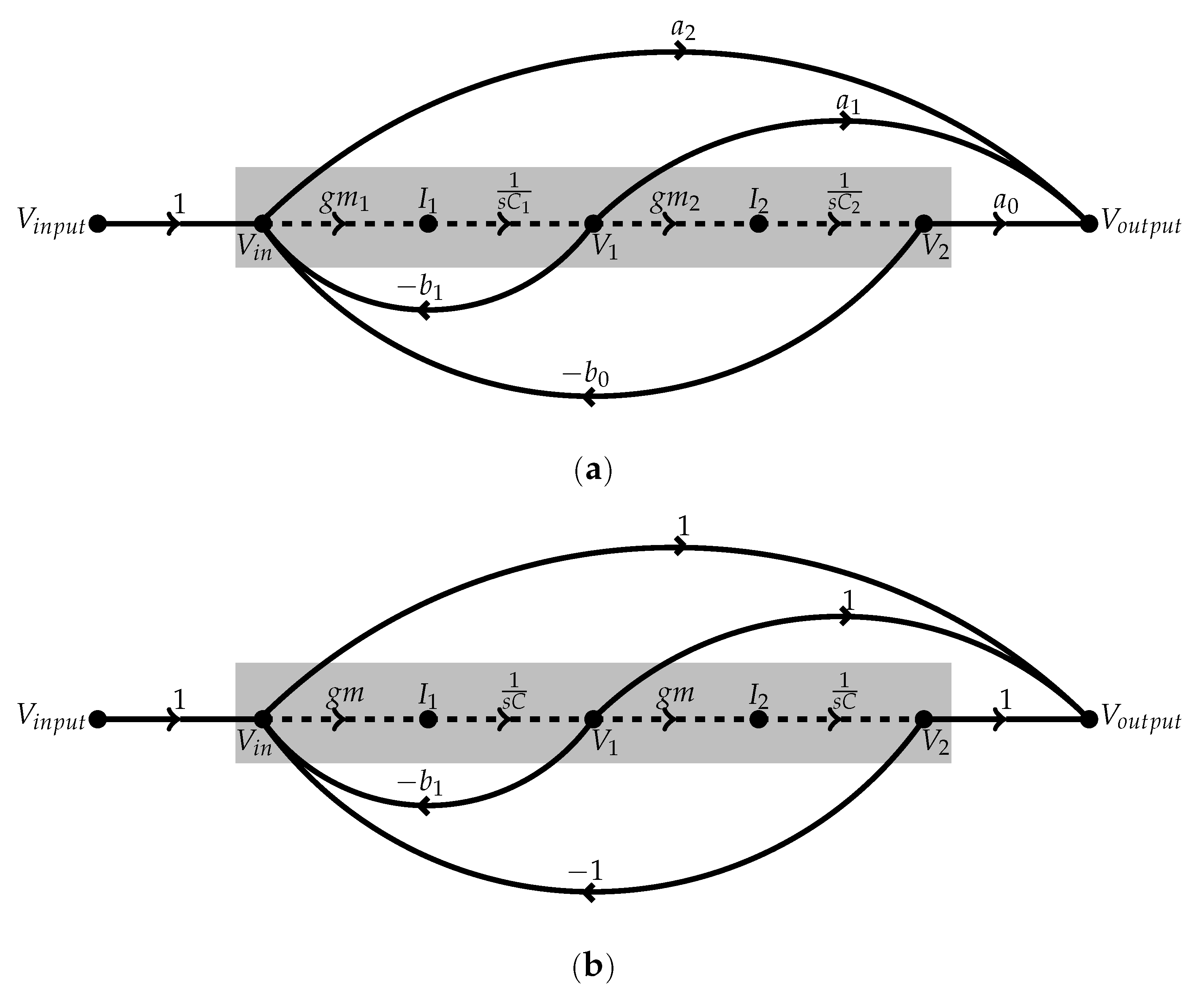
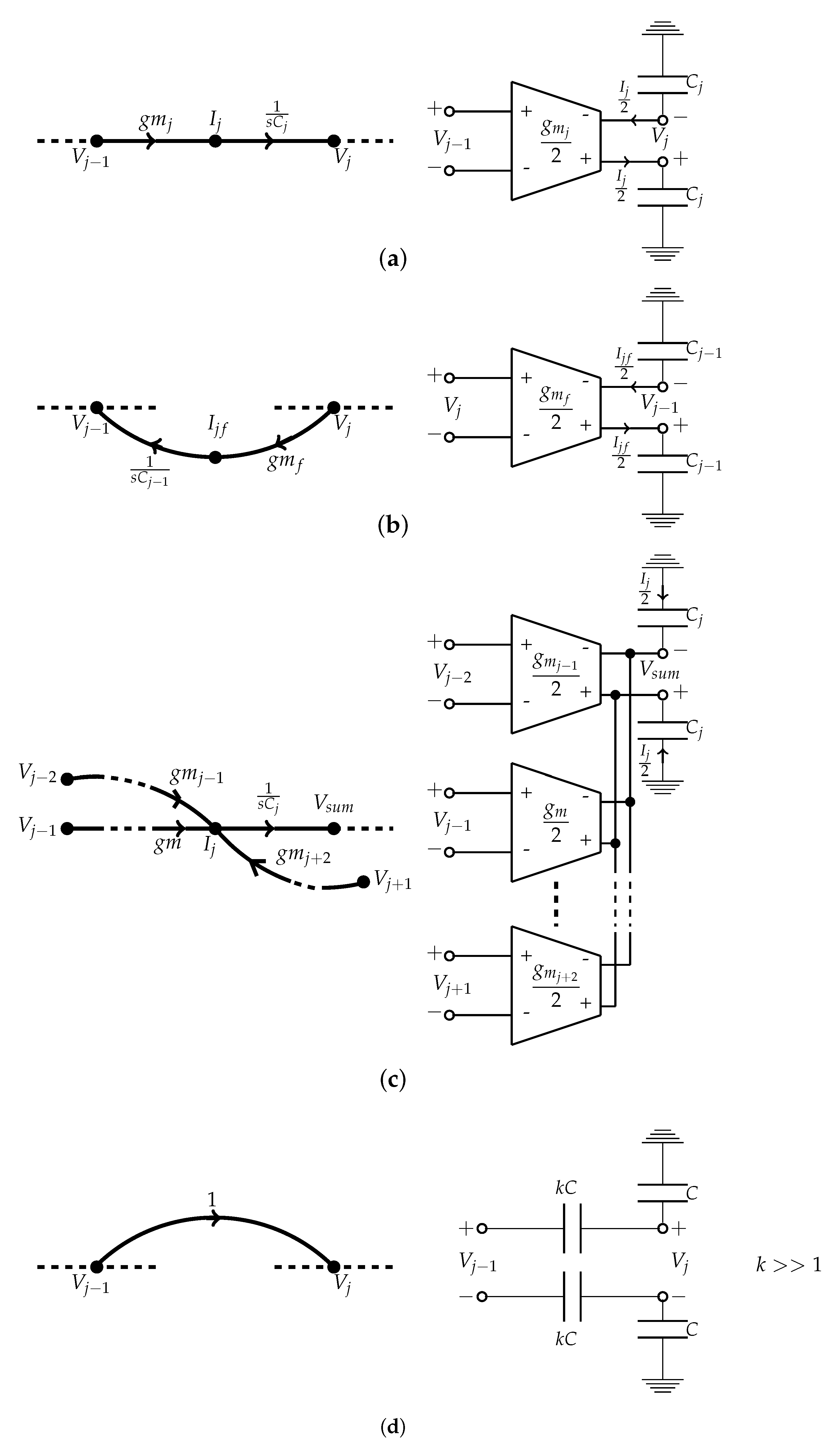
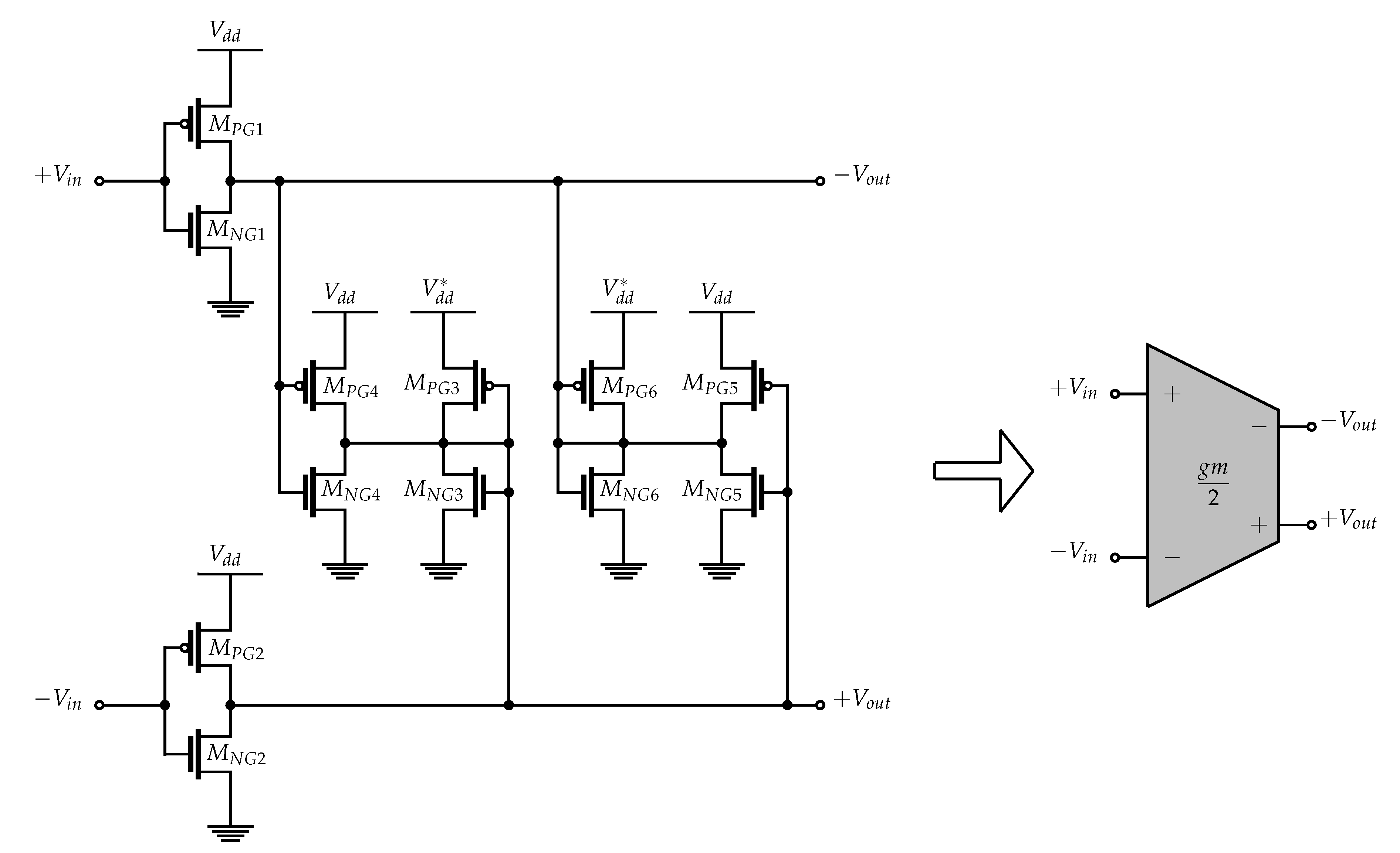
2.2. Synthesis of gm-C Biquad Filters Based on SFGs

If both numerator and denominator polynomials of (1) fulfill the condition that m = n = 2 , then T ( s ) corresponds to the biquad filter case, i.e.,
T ( s ) = a 2 s 2 + a 1 s + a 0 s 2 + b 1 s + b 0
Hence, the low-pass ( a 2 = a 1 = 0 ), high-pass ( a 1 = a 0 = 0 ), band-pass ( a 2 = a 0 = 0 ), band-stop ( a 1 = 0 ) or all-pass responses can be performed. Figure 1b illustrates the SFG of (3) when the input and output nodes are in voltage mode.
In order to compose the SFG of the biquad structure in (3) from a g m -C filter approach, the following changes must be made to the graph in Figure 1b:
  • the forward pathway in every single loop has to be pulled apart into two twigs, one with a path weight g m j , and the other with a path weight ( 1 / s C j ) . The subscript j denotes the j-th transconductance and capacitive reactance along the straight path from node input to node output. Namely, the integrator on the graph is compounded by the product of a transconductance and the reactance of a capacitor.
  • the split-up of the j-th forward pathway within the loops along the graph is achieved by the inclusion of a current node, I k with k = 1 , 2 , 3 , , between the voltage nodes which surround the signal flow on the forth path.
Figure 2a sketches the resulting SFG for the g m -C biquad filter structure obtained by means of the procedure formulated above. When applying the gain formula of Mason in Equation (2) to the graph, it is obtained
T ( s ) = a 2 s 2 + g m 1 C 1 a 1 s + g m 1 g m 2 C 1 C 2 a 0 s 2 + g m 1 C 1 b 1 s + g m 1 g m 2 C 1 C 2 b 0
For simplicity, we take a 2 = a 1 = a 0 = b 0 = 1 , g m 1 = g m 2 = g m , and C 1 = C 2 = C . Such simplification is illustrated in Figure 2b. Thus,
T ( s ) = s 2 + s g m C + g m 2 C 2 s 2 + s g m C b 1 + g m 2 C 2
Herein, the coefficients of the zero and the first order from denominator polynomial are defined as [14]
g m 2 π C = f 0 1 b 1 = Q
where f 0 and Q are the center frequency and the quality factor of the filter, respectively.
The implementation of the SFG of Figure 2b may be accomplished easily by using the building blocks, in fully differential mode, depicted in Figure 3, where the components of the graph, i.e., the integrators, the feedback between two nodes, the signal summation at a node, and the direct pathway between two voltage nodes are posed.

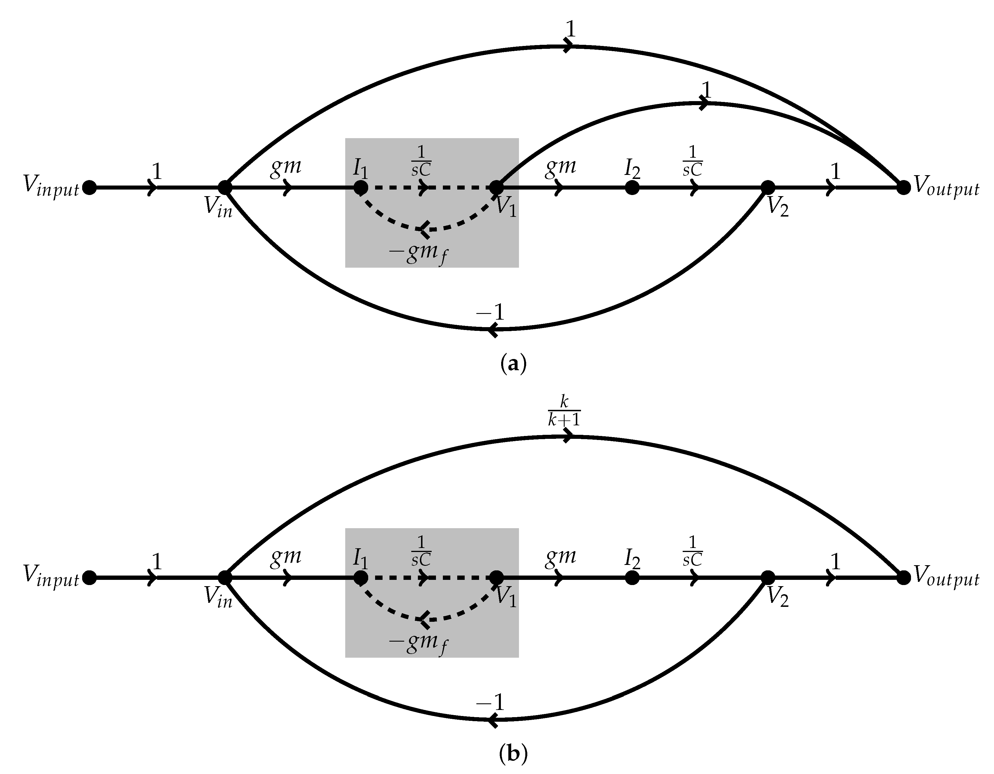
2.3. Increasing Selectivity by SFG Manipulation

By scrutinizing the ratios given in (6), it can be appreciated that selectivity is inversely proportional to b 1 . In this way, as this value decreases, Q rises monotonically and vice versa. Here is where the SFG representation pays off. By inspection of the graph in Figure 2b, it can be seen that the loop gain formed by g m , 1 / s C , and b 1 , among the nodes V i n , I 1 , and V 1 , establishes the first order coefficient from the denominator polynomial of the transfer function expressed in (5). In order to modify the Q of the filter without changing the center frequency, f 0 , neither the value of the transconductance g m nor the capacitance C must be altered. Consequently, b 1 is the only parameter that is allowed to adjust. Manipulation of the loop can be done to redefine Q. Figure 4a exposes the suggested SFG by which the Q of the biquad g m -C filter can be changed independently of f 0 . It can be seen that a new loop between the nodes I 1 and V 1 (dashed lines in Figure 4) has been composed, substituting that formed by branches g m , 1 / s C , and b 1 . The gain of the new loop is given by branches 1 / s C and g m f . By using (2), the transfer function of the new graph is found:
T ( s ) = s 2 + s g m C + g m 2 C 2 s 2 + s g m f C + g m 2 C 2
and now f 0 and Q are expressed as
f 0 = 1 2 π g m C Q = g m g m f
Therefore, f 0 is preserved as in the former case, whereas Q is now the ratio of transconductances g m and g m f . Thus, Q can be tuned within a range by fixing g m to a given value, which is determined by the center frequency of the filter, and varying g m f . From (8), it is clear to see that to achieve high Q values, g m f must be smaller than g m . At this point, it is important to inquire how large the ratio ( g m / g m f ) can be. Numerically, it is possible to choose a ratio as large as 100, for example, but in practice there are limits which make unfeasible that possibility. Since g m is fixed according to f 0 , g m f is the only term in (8) with degree of freedom to be varied. However, the transconductance of any analog architecture in a CMOS process is somehow related to the aspect ratio, ( W / L ), of the transistors that compose it. In fact, the transconductance rises or decreases as ( W / L ) does in either a linear or quadratic fashion [23]. Therefore, a small value of g m f implicates a small ( W / L ) ratio of the transistors involved. There are limits concerning the minimum ( W / L ) ratio in a CMOS design imposed by the design rules of a given process. Consequently, g m f can be smaller than g m to some extent only. Furthermore, if the current of g m f at its output port is delivered to a capacitor load, which is the case for the g m -C filter, then how fast capacitor is charged and discharged plays an important role. The time constant, τ , in g m -C integrators is given by the ( C / g m ) ratio. For the case of f 0 = 400 MHz, the time period of the signal is T 0 = 2.5 n s e c . In case that τ is established, in the worst case, at 40% of T 0 , then τ = 1 n s e c . Considering that C is in the hundred of femto Farads, then g m f must be at most in the dozens of µ℧. Hence, the lower limit for the value of g m f depends on f 0 as well.
Altogether, a considerable Q enhancement with the proposed biquad filter synthesis based on SFG manipulation can be achieved compared to the selectivity exhibited by a regular biquad approach. Simulation results at transistor level of a g m -C structure synthesized by means of the proposal demonstrate that biquad architectures with performance metrics even better than higher order filter structures are conceivable. A band-stop response has been chosen with the aim of realizing the synthesis of a biquad RF notch filter for blocker (Figure 4b). Nevertheless, the Q exhibit the same behavior for any of the approximations (low-pass, high-pass, band-pass, all-pass) since the denominator polynomial of the transfer function of the biquad filter remains the same for all the different responses.

3. An RF Biquad Notch Filter for Jammer
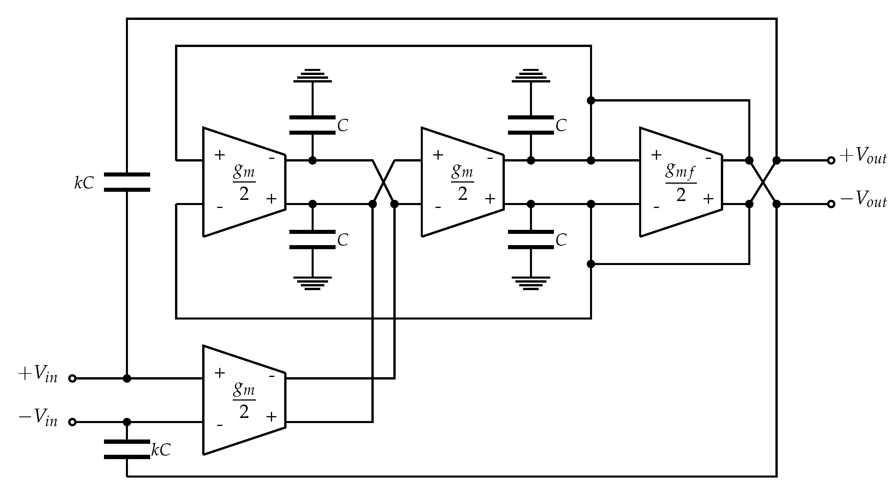
Due to the huge number of wireless devices sharing a given portion of the electromagnetic spectrum and operating in close proximity, a healthy coexistence among diverse communication standards has become a relevant issue. It is possible to have interferers or blockers (also called jammers) as strong as 0dBm, driving almost any receiver in compression [24]. Therefore, RF jammer filtering is needed.

3.1. The biquad g m -C Notch Filter Derived from SFG Synthesis

Since fixed filters are undesired because of their limited Q and tunability, the Q-enhanced bandstop g m -C biquad filter in Figure 5 is proposed, as a design example, for blocker suppression at f 0 = 400 MHz, which is the lower-sideband of the Medical Implant Communication Service (MICS), whose frequency band lies within the (402–405) MHz [25]. Such filter architecture is built up directly from the SFG of Figure 4b for the notch case by interconnecting the fully differential building blocks of Figure 3. By doing this, the following transfer function is produced:
V o u t V i n ( s ) = k k + 1 s 2 + g m 2 C 2 s 2 + s g m f C + g m 2 C 2
whose stop frequency, f 0 , and selectivity, Q, are expressed as in (8). k is the scaling factor from the k C capacitors in Figure 5. It is preferable that k > > 1 , otherwise, f 0 deviates from its nominal value. This is depicted in Figure 6. As can be appreciated, for k = 1 , f 0 experiences a deviation of 42 % of its nominal value; furthermore, when k = 10 , f 0 deviation is 5 % of its nominal value; finally, when k = 100 , f 0 deviation is negligible and it remains at 400 MHz. Thus, by taking k = 100 , the transfer function of the notch filter of Figure 5 becomes
V o u t V i n ( s ) = 0.99 s 2 + g m 2 C 2 s 2 + s g m f C + g m 2 C 2
To achieve operation at the hundreds of MHz, the transconductance g m has to be on the few m℧ while the capacitor values, C, must prevail on the hundreds of femto Farads (parasitics included). As stated earlier, to exhibit a high Q value, transconductance g m f of the Filter has to be, at most, on the dozens of µ℧. These values can be easily managed in the single-poly, 6-metal layers, Mixed-Signal/RF 0.18 µm CMOS technology that was employed for the design of the g m -C biquad.
A simple transconductor topology with a minimum number of internal nodes and consequently with a high frequency of operation was proposed by Bram Nauta in [16]. Even though its major drawback of drawing transient currents from the power supply, which increases the potential of signal coupling between stages [26] as well as exhibiting a considerable power consumption at very high frequencies, with more than 300 citations, papers and patents included, the circuit has proved to be a very useful building block. Figure 7 shows the Nauta transconductor with CMOS devices. As can be seen, it consists of a fully-differential amplifier based on six inverter gates, i.e., six PMOS ( M P G 1 , , P G 6 ) and six NMOS ( M N G 1 , , N G 6 ) transistors. In order to size the transistors of the transconductor, the design trade-offs among important parameters such as low frequency gain, distortion, signal swing available, dissipation and frequency limitations must be considered according to the recommendations in [14]. By doing so, and aiming at transconductance values of ( g m / 2 ) = 500 µ℧ and ( g m f / 2 ) = 25 µ℧, the following aspect ratios arise: ( W M N G 1 , , N G 6 L ) = ( 14.04 μ m 0.18 μ m ) and ( W M P G 1 , , P G 6 L ) = ( 42.3 μ m 0.18 μ m ) . The C capacitors are meant to be on chip with a capacitance of 200 fF (parasitics included); meanwhile, the k C capacitors are chosen to be off-chip with a capacitance of 20 pF. The bias voltage, V d d , is set to a value 1.8 V. The layout of the filter is shown in Figure 8; it was done in the CADENCE IC6.1.6.101 Virtuoso design environment. The total occupied area of the filter is 0.004282 mm2, with a length of 86.61 µm and a width of 49.44 µm. Capacitors, C, are Metal–Insulator–Metal (MIM) Capacitors. In Section 4, the post layout simulation results of the proposal are reported.

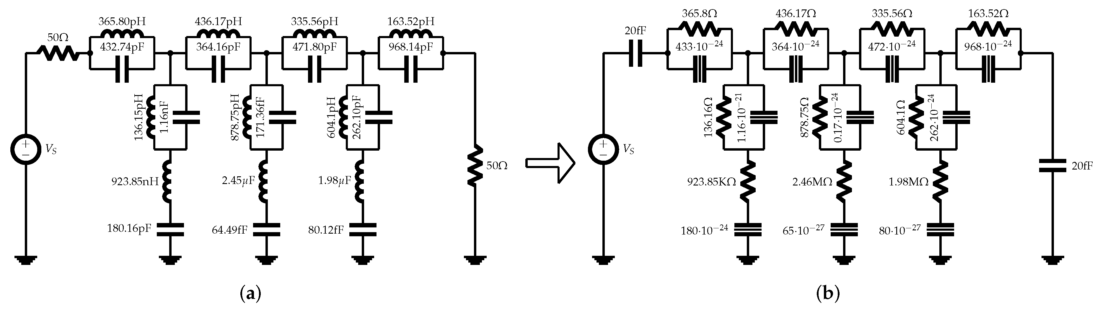
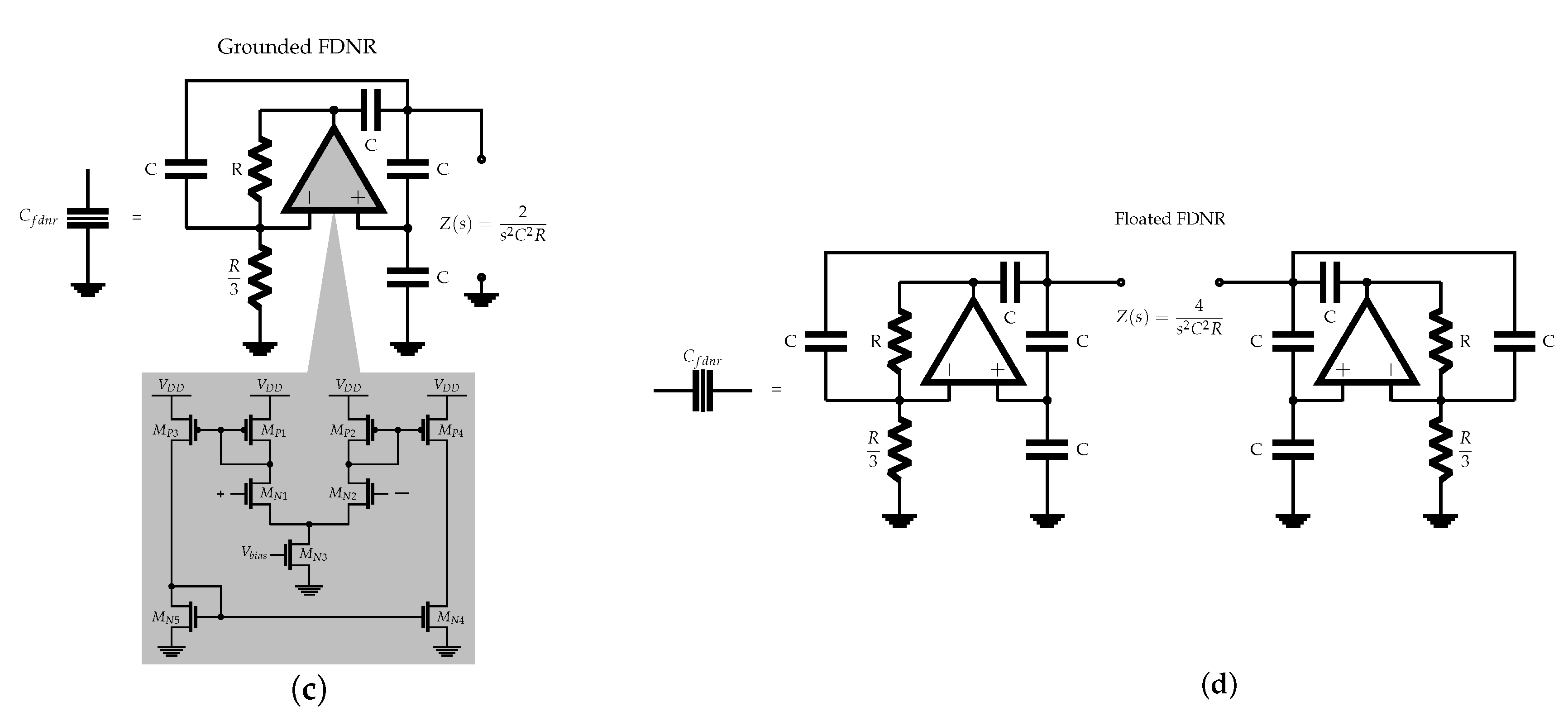
3.2. The Alternative Filter Solution Based on Active Simulation of Passive LC Networks

Before presenting the performance features of the proposed CMOS band-stop biquad filter, it is important to point out that there are systematic approaches other than the structural simulation method based on the use of the SFGs to synthesize active filters [27]. One possibility is to break the desired transfer function, obtained by some known approximation method like Butterworth, Chebyshev, Cauer, Bessel–Thomson, or Pascal, into the product of first and second order transfer functions with either real or complex conjugate poles; then, these low-order transfer functions are implemented with active structures through the use of operational amplifiers (OPAMPs), transconductance amplifiers (OTAs), Current Conveyors (CCs), etc.; finally, the active structures are cascaded to obtain the wanted transfer function. Probably, the most popular synthesis methodology of active filters is the one based on active simulation of passive L C networks with double resistive termination. Such approach can be done by performing the direct replacement of inductors in the L C ladder network by general impedance converters (GICs) or the scaling of frequency dependent impedances in the ladder network. In order to compare the suggested SFG based notch biquad filter with other solutions, the design of a fllter based on active simulation of passive L C networks with double resistive termination was carried out. Figure 9a shows the circuit diagram of an L C T-ladder network with double resistive termination corresponding to a 7th order elliptic band-stop filter with a notch frequency of 400 MHz. This filter was designed to exhibit a transfer function order as low as possible with a band-pass ripple of 0.1 dB, a notch depth larger than 15 dB and a Q 20 . A total of 10 inductors and 10 capacitors are needed to build up the ladder network. Unfortunately, inductors are not an easy target in a CMOS process and the area demanded by them is rather large. Thus, a Frequency Dependent Negative Resistor (FDNR) transformation was performed (Figure 9b) such that there are only resistors, capacitors and grounded and floated supercapacitors in the T-ladder network. The supercapacitors can be realized in active form such as it is depicted in Figure 9c,d. The grounded version of supercapacitor in Figure 9c shows a possibility to be accomplished with CMOS transistors. This CMOS amplifier can be used as well in the floated version of supercapacitor in Figure 9d. In that case, a total of 17 amplifiers are required. For this particular design, the following aspect ratios of the transistors in the amplifier were used: ( W M N 1 , 2 L ) = ( 68.76 μ m 0.36 μ m ), ( W M N 3 L ) = ( 17.28 μ m 0.36 μ m ), ( W M N 4 , 5 L ) = ( 8.64 μ m 0.36 μ m ), ( W M P 3 , 4 L ) = ( 1.8 μ m 0.36 μ m ), ( W M P 1 , 2 L ) = ( 1.08 μ m 0.36 μ m ), V D D = 1.8 V and V b i a s = 0.6 V.

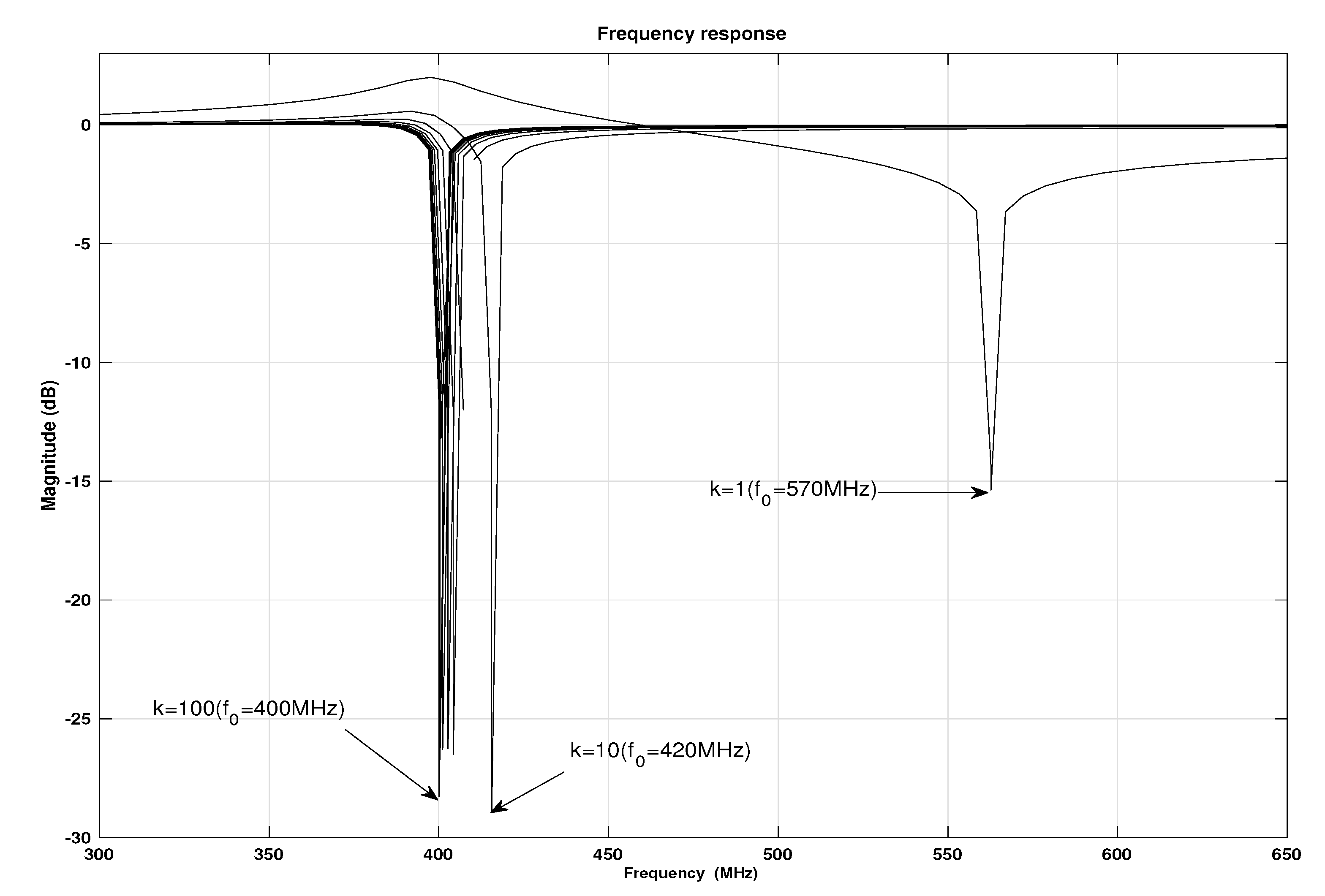
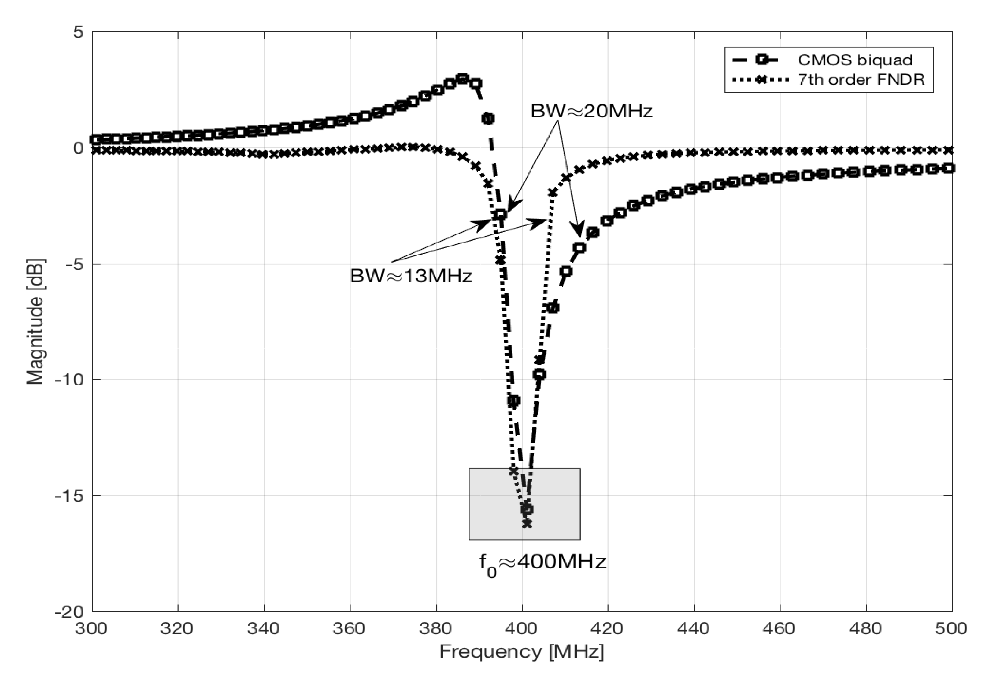
4. Simulation Results

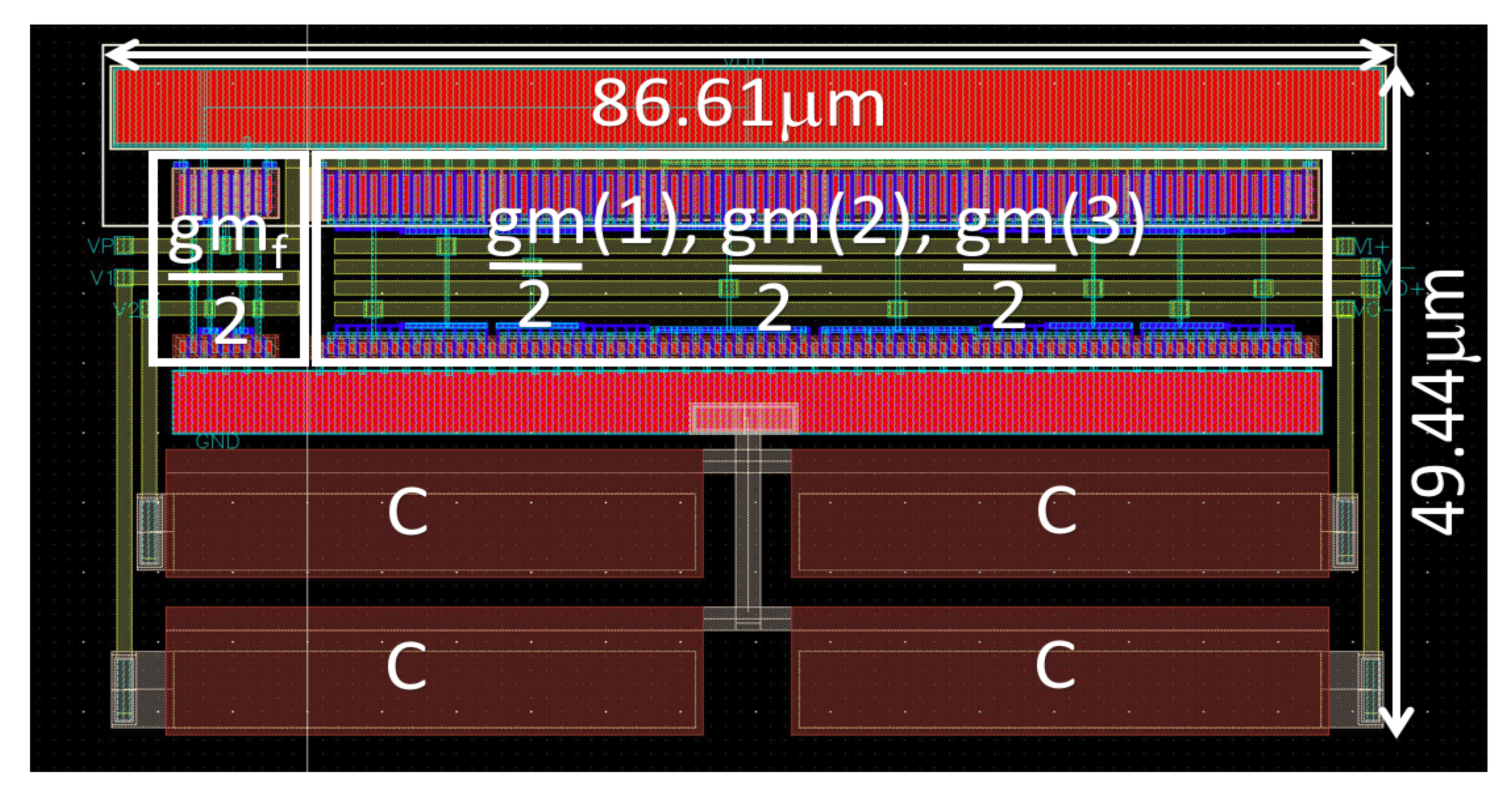
4.1. Post Layout Simulation

Post layout simulation of the proposed biquad notch filter was performed with the aid of the Cadence IC6.1.6.101 Spectre analog design environment. Furthermore, simulation of the FDNR active filter of Figure 9b in active form was also carried out in the single-poly, 6-metal layers, Mixed-Signal/RF 0.18 µm CMOS technology. The attained results are summarized in Table 1 along with some other state-of-the-art band-stop filters. From those, the proposals [28,29,30] report simulation results based on CMOS circuits, whereas approach [31] accounts for experimental results based on lumped resonators. The latter is the filter whose center frequency, f 0 , is the larger, closely followed by the biquad and FDNR filters presented in this work. The f 0 of the rest of the approaches are at least one order of magnitude smaller. In addition, since acoustic-wave-lumped resonators are employed in [31], this is the proposal with the larger Q of all the filters in Table 1, at the expense of a null tunability. The applications for which the filters reported somewhere else are referred only in [29] (Bluetooth), the rest do not specify where the design efforts were directed to. On the other hand, both the SFG based and the FNDR filters reported herein are intended for the Medical Implant Communication Service (MICS), whose frequency band lies within the (402–405) MHz [25].
Figure 10 shows the frequency response of the magnitude of both the suggested SGF CMOS biquad and the 7th order FDNR. As can be seen, these achieve a maximum attenuation of ~−17 dB at the notch frequency (≈400 MHz); however, the FDNR filter exhibits a narrower BW (≈13 MHz) compared to the SFG biquad ( B W 20 MHz) but with a larger power consumption and filter complexity. This was expected since a higher filter order with ripple in the bandpass renders a higher selectivity; however, the reached selectivity ( Q = 20 ) of the proposed architecture is a good quality factor for a biquad, even though the NAM based biquad in [28] reports a Q of 50 for a rather low frequency of operation f 0 = 2 KHz. A Q = 20 was also achieved in [29]; nevertheless, a third order approach was used and hence the circuit possesses a steeper slope (20 dB/Dec sharper). Otherwise, the notch depth reported in [28,29,30] is optimistic; even with a very narrowband like those in [31], the achieved rejection barely surpasses the −20 dB. Thus, the −17 dB accomplished by the two circuit topologies described here is more realistic; it is not uncommon to have RF jammer filters with a notch depth barely larger than −10 dB.
In terms of tunability, the filter in [29] is comparable to the SFG biquad and the FDNR; however, these work at a higher frequency. Unfortunately, none of the filters in Table 1 reported somewhere else present distortion measures ( T H D , I M 3 , I I P 3 ); on the contrary, the SFG biquad and the FDNR reported herein exhibits a good linearity with +15 dBm and +12 dBm IIP3, respectively. Again, sensitivity is not reported in the rest of the filters, but, for our case, the SFG biquad is more sensitive compared to the FDNR, as expected since the latter active architecture is synthesized from a passive network. Finally, power consumption is the drawback of the proposal. Both the SFG biquad and the FDNR are the most power hungry among the filters in Table 1. Though there is the chance to scale the value of g m and C to some extent to lower power consumption, by doing so, maintaining the performance of the filter is troublesome. Since the dissipation of any g m -C filter is strongly determined by the dissipation of its transconductances, and for the case of the Nauta transconductor employed herein the power dissipation can be reduced by lowering the bias supply, then less V d d is favorable for the dissipation of the proposed biquad notch; unfortunately, when V d d goes down the cutoff frequency of the transconductor does as well. Actually, the results reported in [16] for the case of a third order elliptic low-pass derived from a passive ladder show that for an ≈75% decrease of V d d the power consumption is lessened ≈ 90% at the expense of an ≈77% cutoff frequency reduction. Regarding the used CMOS technology and its impact on the power consumption of the proposal, the following question arises: is it possible to significantly reduce the power dissipation of the proposed filter structure if a more advanced technology, say 65 nm, is used? The answer is that the power consumption would be moderately reduced. The reason is that g m -C filters are, typically, noise and open-loop distortion dominated circuits whose performance parameters such as the power dissipation do not show dependence on technology scaling as long as the signal-swing scales down as the supply voltage diminishes [32]. By glancing at some published works about g m -C filters and Nauta transconductors in 65 nm [33,34,35], power dissipation in the tens of milliwatts are reported, which are slightly smaller than the ≈52 mW exhibited by the proposal in 180 nm. Thus, if power consumption is an issue, it is recommended to use a g m -C topology other than the biquad employed here; for instance, a more energy efficient g m -C structure for low-order filtering is reported in [36].
It is important to remark that practical loading to the filter is beneficial in order to verify its driven capability. However, in the proposed filter structure, this was ignored since the scope of the research is to provide a methodology for synthesizing high-selectivity/low-order biquad g m -C filters by means of SFG manipulation instead of focusing on the I/O buffering needs of a practical realization. However, this can be covered with the inclusion of a driver stage, a programmable gain amplifier (PGA) for instance. Some filter designs include both the filter structure and the PGA, especially if energy efficiency is relevant [36].

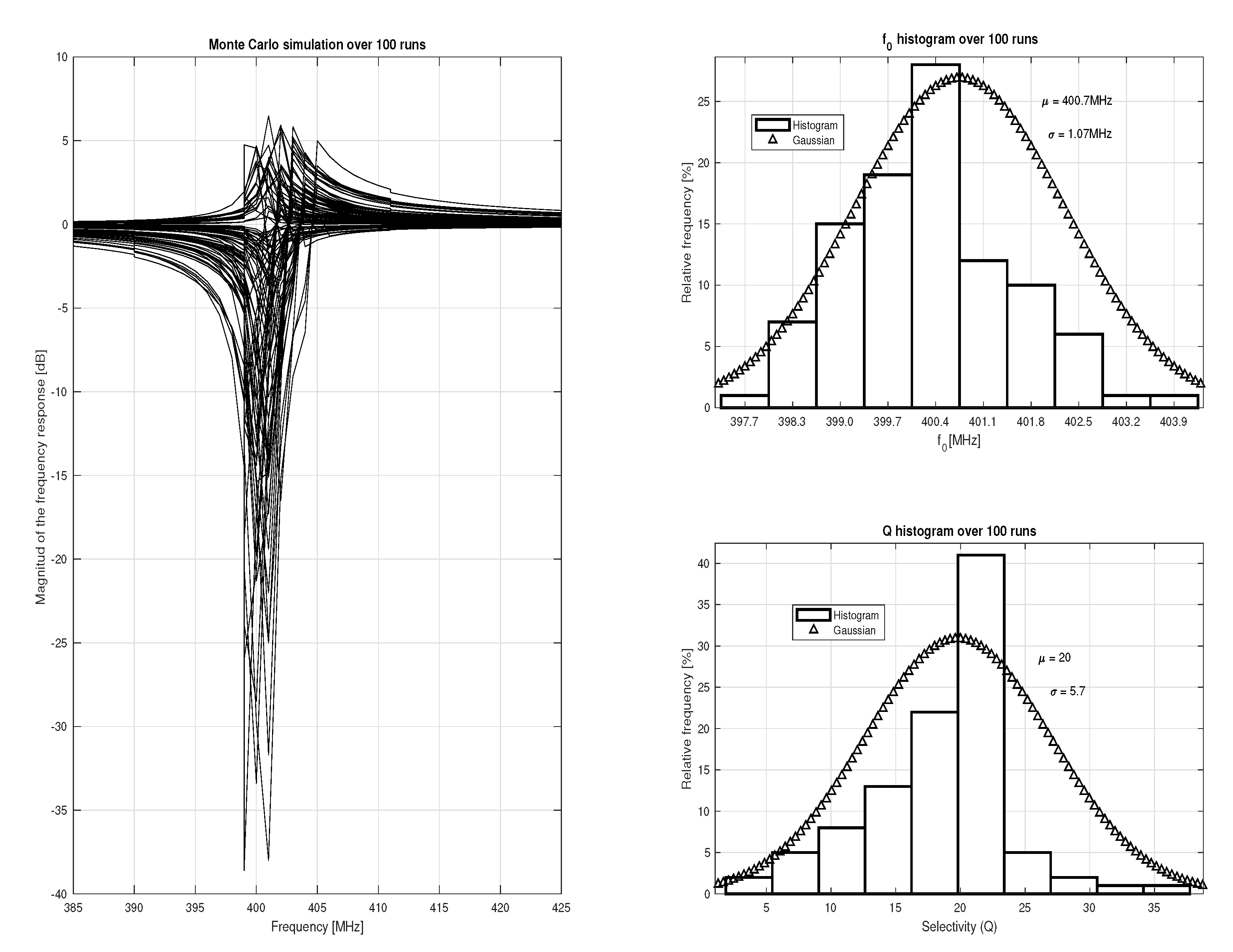
4.2. Monte Carlo Simulation

On the other hand, to verify the robustness of the proposal under the presence of mismatch, Monte Carlo simulations based on the model of Pelgrom were conducted. Figure 11 shows the Monte Carlo simulation of the SFG biquad. On the left side, there is the frequency response of the filter. On the right side, at the top, there is the f 0 histogram over 100 runs. Again, on the right side, but at the bottom, there is the Q histogram over 100 runs. As can be seen, the mean is 400.7 MHz for the f 0 with a standard deviation of 1.07 MHz. Thus, the center frequency has a nominal value of ~400 MHz with a tolerance of ±0.25%. On the other hand, the mean is 20 for the Q with a standard deviation of 5.7. Hence, deviation is larger for selectivity compared to f 0 . The mean value of Q is 20 and ~95% of the variations of Q lie between 8.6 and 31.4.

5. Conclusions

The synthesis of high performance biquad g m -C filters by means of SFG manipulation has been presented. The SFG representation of a transfer function in canonical form is formulated along with the methodology to build up this transfer function in a fully differential g m -C circuit. As a practical example, the design of a g m -C notch biquad filter intended to suppress interferers in the lower sideband (400 MHz) of the Medical Implant Communication Service (MICS), in a single-poly, 6-metal layers, Mixed-Signal/RF 0.18 µm CMOS technology was realized. Additionally, to compare the performance of the proposed notch biquad with an FDNR solution, the design of an active 7th order elliptic notch filter was also accomplished. The attained simulation results prove that the proposal is competitive compared to both the FDNR solution and some other state-of-the-art filters reported in the literature. The most salient features of the proposed notch biquad filter include: the selectivity, whose value is comparable to the quality factor of a 7th order elliptic approach and some other 3rd order filter architectures; a high-frequency operation avoiding the use of resonators; linearity, with a +15 dBm I I P 3 ; a reduced form factor with a total occupied area of 0.004282 mm2; and a low design complexity. Monte Carlo simulation based on the model of Pelgrom over 100 runs show that the center frequency of the proposal has a nominal value of f 0 = 400 MHz with a tolerance of ± 0.25 % ; meanwhile, the mean value of the Q = 20 with ~95% of the variations between 8.1 and 31.4. Finally, power consumption of the proposal may be troublesome in the case that low power consumption is wanted; in that case, the recommendation is to use a different g m block other than the transconductor of Nauta, whose main drawback is its considerable power consumption.

Author Contributions

Conceptualization, L.A.S.-G., C.M.-M., J.M.M.-P., C.S.-L., L.d.C.G.-P., A.L.-R., and A.I.B.-C.; methodology, L.A.S.-G., C.M.-M., J.M.M.-P., C.S.-L., L.d.C.G.-P., A.L.-R., and A.I.B.-C.; validation, L.A.S.-G., C.M.-M., J.M.M.-P., C.S.-L., L.d.C.G.-P., A.L.-R., and A.I.B.-C.; formal analysis, L.A.S.-G., C.M.-M., J.M.M.-P., C.S.-L., L.d.C.G.-P., A.L.-R., and A.I.B.-C.; investigation, L.A.S.-G., C.M.-M., J.M.M.-P., C.S.-L., L.d.C.G.-P., A.L.-R., and A.I.B.-C.; writing—original draft preparation, L.A.S.-G., C.M.-M., J.M.M.-P., C.S.-L., L.d.C.G.-P., A.L.-R., and A.I.B.-C.; writing—review and editing, L.A.S.-G., C.M.-M., J.M.M.-P., C.S.-L., L.d.C.G.-P., A.L.-R., and A.I.B.-C. All authors have read and agreed to the published version of the manuscript.

Funding

This research received no external funding.

Conflicts of Interest

The authors declare no conflict of interest.

References

  1. Eastman, A.V. The Application of Filter Theory to the Design of Reactance Networks. Proc. IRE 1944, 9, 538–546. [Google Scholar] [CrossRef]
  2. Belevitch, V. Recent Developments in Filter Theory. IRE Trans. Circuit Theory 1958, 4, 236–252. [Google Scholar] [CrossRef]
  3. Belevitch, V. Summary of the History of Circuit Theory. Proc. IRE 1962, 5, 848–855. [Google Scholar] [CrossRef]
  4. Tsai, W.-C.; Tsai, W.-C.; Shih, Y.-J.; Huang, N.-T. Hardware-Accelerated, Short-Term Processing Voice and Nonvoice Sound Recognitions for Electric Equipment Control. Electronics 2019, 9, 924. [Google Scholar] [CrossRef] [Green Version]
  5. Camarena, J.-G.; Gregori, V.; Morillas, S.; Sapena, A. Some improvements for image filtering using peer group techniques. Elsevier Image Vis. Comput. 2010, 1, 188–201. [Google Scholar] [CrossRef]
  6. Tan, L.; Pugh, A.C.; Yin, M. Rate-based congestion control in ATM switching networks using a recursive digital filter. Elsevier Control Eng. Pract. 2003, 10, 1171–1181. [Google Scholar]
  7. Wang, B.; Cao, Z. A Review of Impedance Matching Techniques in Power Line Communications. Electronics 2019, 8, 1022. [Google Scholar] [CrossRef] [Green Version]
  8. Chinnasamy, C.; Malallah, Y.; Jasinski, M.M.; Daryoush, A.S. Synthesis of high magnetic moment soft magnetic nanocomposite powders for RF filters and antennas. Elsevier Appl. Surf. Sci. 2015, 334, 58–61. [Google Scholar] [CrossRef]
  9. Xu, L.; Feng, D.; Wang, X. Matched-filter properties of linear-frequency-modulation radar signal reflected from a phase-switched screen. IET Radar Sonar Navig. 2016, 2, 318–324. [Google Scholar] [CrossRef]
  10. Saberkari, A. Active inductor-based tunable impedance matching network for RF power amplifier application. Elsevier Integr. VLSI J. 2016, 52, 301–308. [Google Scholar] [CrossRef] [Green Version]
  11. Piccinni, G.; Talarico, C.; Avitabile, G.; Coviello, G. Innovative Strategy for Mixer Design Optimization Based on gm/ID Methodology. Electronics 2019, 8, 954. [Google Scholar] [CrossRef] [Green Version]
  12. Rachid, M.; Pamarti, S.; Daneshrad, B. Filtering by Aliasing. IEEE Trans. Signal Process. 2013, 9, 2319–2327. [Google Scholar]
  13. Fox, R. Continuous-time filters. In Trade-Offs in Analog Circuit Design: The Designers Companion; Toumazou, C., Moschytz, G.S., Gilbert, B., Eds.; Kluwer Academic Publishers: Berlin, Germany, 2002; pp. 344–347. [Google Scholar]
  14. Nauta, B. Analog CMOS Filters for Very High Frequencies. Ph.D. Thesis, Twente Universiteit, Enschede, The Netherlands, 1991. [Google Scholar]
  15. Gee, W.A. CMOS Integrated LC Q-Enhanced RF Filters for Wireless Receivers. Ph.D. Thesis, ECE, GATECH, Atlanta, GA, USA, 2005. [Google Scholar]
  16. Nauta, B. A CMOS transconductance-C filter technique for very high frequencies. IEEE J. Solid-State Circuits 1992, 2, 142–153. [Google Scholar] [CrossRef] [Green Version]
  17. Kwon, K. A 50- to 300-MHz CMOS Gmmbox-C Tracking Filter Based on Parallel Operation of Saturation and Triode Transconductors for Digital TV Tuner ICs. IEEE Trans. Circuits Syst. II Express Briefs 2015, 6, 522–526. [Google Scholar] [CrossRef]
  18. Acosta, L.; Jimenez, M.; Carvajal, R.G.; Lopez-Martin, A.J.; Ramirez-Angulo, J. Highly linear tunable CMOS gm-C low-pass filter. IEEE Trans. Circuits Syst.-I Regul. Pap. 2010, 10, 2145–2158. [Google Scholar] [CrossRef]
  19. Galan, J.; Pedro, M.; Sanchez-Rodriguez, T.; Munoz, F.; Carvajal, R.G. A Very Linear Low-Pass Filter with Automatic Frequency Tuning. IEEE Trans. Very Large Scale Integr. (VLSI) Syst. 2013, 1, 182–187. [Google Scholar] [CrossRef]
  20. Niknejad, A.M. Analysis, Simulation, and Applications of Passive Devices on Conductive Substrates. Ph.D. Thesis, EECS, UCB, Berkeley, CA, USA, 2000. [Google Scholar]
  21. Raut, R.; Swamy, M.N.S. Modern Analog Flter Analysis and Design: A Practical Approach, 1st ed.; Wiley: Hoboken, NJ, USA, 2010; pp. 1–7. [Google Scholar]
  22. Lin, P.-M. Signal flow graphs in filter analysis and synthesis. In Circuit Analysis and Feedback Amplifier Theory; Chen, W.-K., Ed.; CRC Press: Boca Raton, FL, USA, 2006; pp. 4.1–4.20. [Google Scholar]
  23. Maloberti, F. Analog Design for CMOS VLSI Systems, 1st ed.; Kluwer Academic Publishers: Berlin, Germany, 2003. [Google Scholar]
  24. Ghaffari, A.; Klumperink, E.; Nauta, B. 8-path tunable RF notch filters for blocker suppression. In Proceedings of the International Conference on Solid-State Circuits (ISSCC 2012), San Francisco, CA, USA, 19–23 February 2012; pp. 76–78. [Google Scholar]
  25. Islam, M.N.; Yuce, M.R. Review of Medical Implant Communication System (MICS) Band and Network; Elsevier ICT Express: Wilnecote, UK, 2016. [Google Scholar]
  26. Mondal, I.; Krishnapura, N. Gain enhanced high frequency OTA with on-chip tuned negative conductance load. In Proceedings of the IEEE International Symposium on Circuits and Systems (ISCAS), Oslo, Norway, 26–28 October 2015; pp. 2085–2088. [Google Scholar]
  27. Dimopoulos, H.G. Even-Order Passive filters: Pascal versus Chebyshev. Wiley Int. J. Circuit Theory Appl. 2013, 9, 946–959. [Google Scholar] [CrossRef]
  28. Tran, H.-D.; Wang, H.Y.; Nguyen, Q.M.; Chiang, N.H.; Lin, W.C.; Lee, T.F. High-Q biquadratic notch filter synthesis using nodal admittance matrix expansion. Elsevier Int. J. Electron. Commun. (AEU) 2015, 7, 981–987. [Google Scholar] [CrossRef]
  29. Yehoshuva, C.; Reddy, B.N.; Ambati, V.R.; Pittala, S.K. A novel CMOS Gm-C complex filter design for multi-mode multi band wireless receiver applications. Springer Analog Integr. Circuits Signal Process. 2017, 1, 43–51. [Google Scholar] [CrossRef]
  30. Roja, K.; Santhoshini, K.M.; Sarada, M.; Srinivasulu, A. A constant Q-factor notch filter using voltage difference transconductance amplifier. Elsevier Solid State Electron. Lett. 2019, 1, 38–43. [Google Scholar]
  31. Psychogiou, D.; Gómez-García, R.; Peroulis, D. High-Q Bandstop Filters Exploiting Acoustic-Wave-Lumped-Element Resonators (AWLRs). IEEE Trans. Circuits Syst. II Express Briefs 2016, 1, 79–83. [Google Scholar] [CrossRef]
  32. Bult, K. The effect of technology scaling on power dissipation in analog circuits. In Analog Circuit Design, RF Circuits: Wide Band, Front-End, DACs, Design Methodology and Verification for RF and Mixed-Signal Systems, Low Power and Low Voltage; Steyaert, M., van Roermund, A.H.M., Huijsing, J.H., Eds.; Springer: Dordrecht, The Netherlands, 2006; pp. 251–294. [Google Scholar]
  33. Jolivet, S.; Amiot, S.; Lohy, D.; Jarry, B.; Lintignat, J. A 45–470MHz Gm-C tunable RF bandpass filter for TV tuners designed in 65 nm CMOS. In Proceedings of the IEEE 9th International New Circuits and Systems Conference, Bordeaux, France, 26–29 June 2011; pp. 13–16. [Google Scholar]
  34. Lee, H.; Seo, H.; Choi, I.; Chung, T.; Jeong, D.; Kim, B. A RF CMOS band-pass tracking filter with enhanced Q and high linearity. In Proceedings of the Asia-Pacific Microwave Conference, Melbourne, Australia, 5–8 December2011; pp. 1901–1904. [Google Scholar]
  35. Nicholson, A.P.; Iberzanov, A.; Jenkins, J.; Hamilton, T.J.; Lehmann, T. A Statistical Design Approach for a Digitally Programmable Mismatch-Tolerant High-Speed Nauta Structure Differential OTA in 65-nm CMOS. IEEE Trans. Very Large Scale Integr. (VLSI) Syst. 2016, 9, 2899–2910. [Google Scholar] [CrossRef]
  36. Liu, H.; Zhu, X.S.; Lu, M.; Sun, Y.; Yeo, K.S. Design of reconfigurable dB-linear variable-gain amplifier and switchable-order gm-c filter in 65-nm CMOS technology. IEEE Trans. Microw. Theory Tech. 2019, 12, 5148–5158. [Google Scholar] [CrossRef]
Figure 1. SFG in controllable canonical form of: (a) a general transfer function, and (b) a second order transfer function.
Electronics 09 00362 g001
Figure 2. SFGs in controllable canonical form of a biquad gm-C filter: (a) complete and (b) simplified graphs.
Electronics 09 00362 g002
Figure 3. Fully differential building blocks: (a) integrators; (b) feedback twig between two nodes; (c) current addition at a node and its conversion to a voltage node; (d) a direct pathway with unity gain between two voltage nodes.
Electronics 09 00362 g003
Figure 4. SFGs in controllable canonical form of: (a) the proposed general gm-C biquad filter structure; (b) the proposed notch gm-C biquad filter.
Electronics 09 00362 g004
Figure 5. Q enhanced bandstop gm-C biquad filter.
Electronics 09 00362 g005
Figure 6. Frequency shift produced by the scaling factor, k of the k C capacitors.
Electronics 09 00362 g006
Figure 7. CMOS circuit used as transconductor.
Electronics 09 00362 g007
Figure 8. Layout of the proposed CMOS notch biquad in a CADENCE IC6.1.6.101 Virtuoso design environment.
Electronics 09 00362 g008
Figure 9. 7th order elliptic notch filter at 400 MHz: (a) L C network with double resistive termination; (b) FDNR conversion; (c) grounded version of active supercapacitor C f d n r ; (d) floated version of active supercapacitor C f d n r .
Electronics 09 00362 g009aElectronics 09 00362 g009b
Figure 10. Frequency response of both the suggested SFG CMOS biquad and the 7th order FDNR.
Electronics 09 00362 g010
Figure 11. Monte Carlo simulation of f 0 and Q of the proposed SFG biquad. On the left, there is the frequency response of the filter. On the right, at the top, there is the f 0 histogram over 100 runs. On the right, at the bottom, there is the Q histogram over 100 runs.
Electronics 09 00362 g011
Table 1. Summary of simulation results and performance comparison.
ParameterNAM aAWLRs bgm-CVDTA cFDNR dSFG e
[28][31][29][30]This WorkThis Work
f 0 2 KHz418 MHz20 MHz4.867 MHz400 MHz400 MHz
Q50≈10,0002013120
ConsumptionNR fNR f580 µW540 µW≈220 mW≈52 mW
Technology [µm]0.35CMOSRO4003Csub.0.18CMOS0.18CMOS0.18CMOS g0.18CMOS g
Type (order)biquad (2)BVD h (3)gm-C (3)biquad (2)Elliptic (7)biquad (2)
Rejection−60 dB≈−24 dB≈−40 dB−60 dB≈−17 dB≈−17 dB
Tuning(1.5–2.5) KHznot tunable(10–25) MHzNR f(381.8–400) MHz(394.2–400) MHz
DistortionNR fNR fNR fNR fm I I P 3 > 12 dBmm I I P 3 > 15 dBm
SensitivityNR fNR fNR fNR f S R S , R L T ( s ) = j S g m , C f 0 = ± 1 k
98 × 10 6 S g m , g m f Q = ± 1 l
ApplicationNR fNR fBluetoothNR fMICS iMICS i
a Nodal Admittance Matrix (NAM) Expansion; b Acoustic-Wave-Lumped-Element Resonators (AWLRs); c Voltage Difference Transconductance Amplifier (VDTA); d Frequency Dependent Negative Resistor (FDNR); e Signal Flow Graph (SFG); f No reported; g Mixed-Mode/RF; h Butterworth-Van Dyke (BVD); i Medical Implant Communication Service (MICS); j If R S or R L rise 1% of their nominal value, T ( s ) decreases or increases ≈ 0.000001% of its nominal value, respectively; k If g m or C rise 1% of their nominal value, f 0 increases or decreases 1% of its nominal value, respectively; l If g m or g m f rise 1% of their nomimal value, Q increases or decreases 1% of its nominal value, respectively; m f 0 = 400 MHz, two tones at f 1 = f 0 + 40 MHz and f 2 = f 0 + 80 MHz.

