Electrical Characteristics of Bulk FinFET According to Spacer Length
by
 , and
, and
Jinsu Park
1, 
Jaemin Kim
1,
Sanchari Showdhury
1,
Changhwan Shin
1 ,
,
Hwasung Rhee
2,
Myung Soo Yeo
2,
Eun-Chel Cho
1,* and
Junsin Yi
1,* 1
College of Information and Communication Engineering, Sungkyunkwan University, Suwon-Si 16419, Korea
2
Technology Quality and Reliability Foundry Division, Samsung Electronics Co. LTD., Suwon-Si 16677, Korea
*
Authors to whom correspondence should be addressed.
Electronics 2020, 9(8), 1283; https://doi.org/10.3390/electronics9081283
Submission received: 9 June 2020
/
Revised: 1 August 2020
/
Accepted: 6 August 2020
/
Published: 11 August 2020
(This article belongs to the Section Semiconductor Devices)
Abstract
:This paper confirms that the electrical characteristics of FinFETs such as the on/off ratio, drain-induced barrier lowering (DIBL), and sub-threshold slope (SS) can be improved by optimizing the FinFET spacer structure. An operating voltage that can maintain a life of 10 years or more when hot-carrier injection is extracted. An excellent on/off ratio () and the best SS value were found at 64.29 mV/dec with a spacer length of 90 nm. Under hot carrier-injection conditions, the supply voltages that meet the 10-year lifetime condition are 1.11 V, 1.18 V, and 1.32 V for spacer lengths of 40 nm, 80 nm, and 120 nm, respectively. This experiment confirmed that, even at low drain voltages, the shorter is the spacer length, the greater is the deterioration. However, this increasing maximum operating voltage is very small when compared to the increase in the driving voltage required to achieve similar performance when the spacer length is increased; therefore, the effective life is expected to decrease. The results indicate that structural optimization must be performed to increase the driving current of the FinFET and prevent degradation of the analog performance.
1. Introduction
The performance of semiconductors is improved by scaling the gate length up to 10–15 nm [1,2,3]. However, as the distance between source and drain regions decreases, the electric field in the channel increases, while the ability of the gate to control the channel region decreases. This is known as “short channel effect (SCE)”. If the gate length is reduced more than 10–15 nm, it causes source-to-drain direct tunneling, resulting in the degradation of SCE. Previous research work already showed the limitations of the device scaling, and the Drain-Induced-Barrier-Lowering (DIBL) due to SCE [4,5,6,7,8,9,10,11]. As a result, multi-gate FinFETs were introduced to reduce the leakage current and improve the gate controllability of the transistor channel. The FinFET structure also reduces the occurrence of gate-oxide traps and gate critical paths, owing to the reduction of the hot-carrier effect caused by lightly-doped drain (LDD) formation, resulting in a decrease in the gate-induced drain leakage (GIDL). In the off state, the effective channel length is larger than the physical gate length due to the undoped spacer regions. In the on state, the effective channel length is equal to the physical gate length of the device [12,13]. While the introduction of spacer improves the short-channel performance of the devices, drive current is reduced due to higher series resistance in the spacer regions. Furthermore, the parasitic capacitance increases with the increased device transconductance, causing no improvement in unit-gain frequency.
In this work, we tried to solve these problems by optimizing the spacer structure of the FinFET. We present a bulk-Si N-channel FinFET device (bulk N-FinFET) that has desirable transistor characteristics and competitive short-channel performance. The important parameters in bulk N-FinFETs, including DIBL, SS, drive current, and S/D subthreshold off-state leakage current, are combined to reflect the overall performance of the device and provide a criterion for the design of innovative devices.
2. Device Structure and Simulation Setup
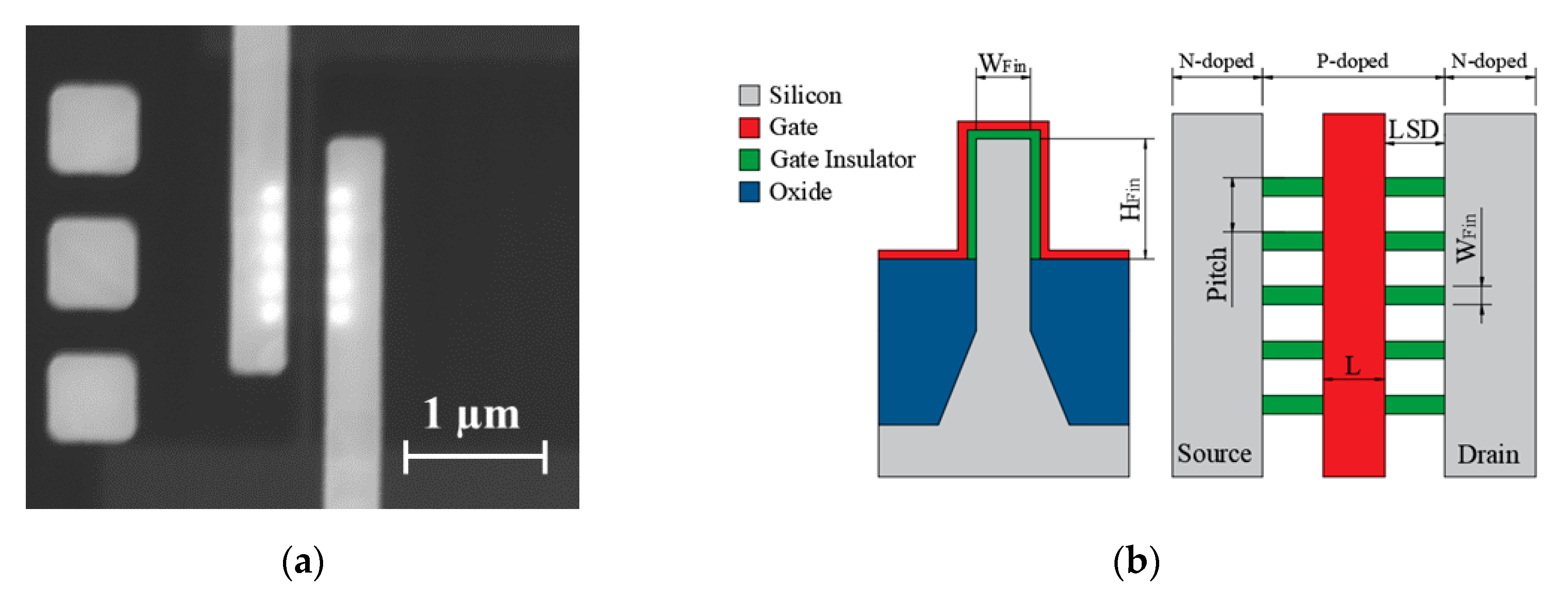
A top-view SEM image of the bulk FinFET used for the measurement is shown in Figure 1a. The important geometrical parameters of a FinFET are defined in Figure 1b, namely the height (Hfin), width (Wfin), transistor length (L), and spacer length (LSD). The device design parameters of the FinFET are summarized in Table 1. These devices feature a high-k gate dielectric (2.3-nm HfSiON on a 1-nm interfacial oxide) and 100 nm of polycrystalline silicon on top of a 5-nm TiN metal gate. The S/D access region is formed by the selective epitaxial growth of Si on the source and drain areas, followed by NiPt silicidation.
To understand the dependence of the electrical properties of a bulk FinFET on the spacer length, 3D TCAD simulations were performed using Atlas TCAD. For device simulation, along with the inversion layer mobility models of Lombardi CVT, SRH, and Auger recombination, LAT.TEMP models were also included. The S/D regions were N-doped at the concentration cm−3 and the channel regions were P-doped at the concentration cm−3.
After applying voltages of 0.1 and 1 V to the drain, the DC simulation of a five-fin FinFET structure was performed, and the on/off current, DIBL, SS, and lattice temperatures were extracted using the Ids–Vgs graph for changes in the spacer length.
3. Results and Discussion
3.1. Off-State Leakage Current
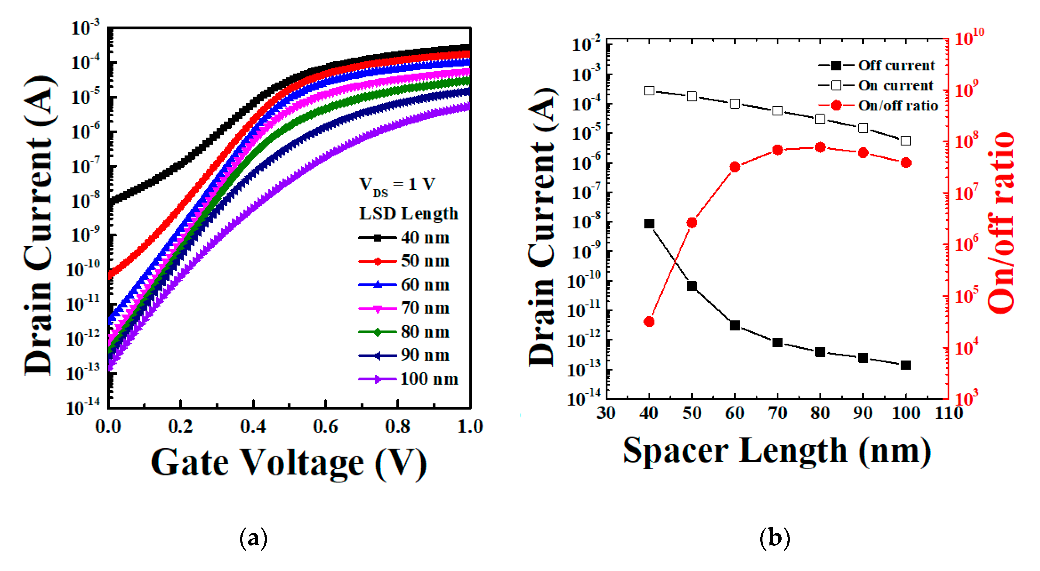
Figure 2 shows the transfer curve and on/off current change according to the spacer length change in a bulk N-FinFET. As the spacer length increases, the source and drain resistances also increase. The increase in source resistance causes the degradation in on-state current. For low-power operation, the spacer length should be designed to be as short as possible. However, when the spacer length becomes shorter than 60 nm, the effective channel length decreases rapidly resulting in the increase in leakage current. Therefore, when the spacer length is 80 nm, the on/off ratio will be the highest, at . Further increase in spacer length increases the source and drain resistance and the increased source resistance causes the degradation in on-state current.
Figure 3 shows the changes in the DIBL and SS with changes in the spacer length. As the length of the spacer increases, the effective channel length increases. In addition, the length of the space-charge region formed at the interface between the channel and drain also increases, and, thus, the DIBL decreases. On the other hand, as the size of the electric field from the drain to the channel region decreases and the total volume of the depletion region increases, it is causing the problem of an increase of the SS. As indicated in Table 2, when the spacer length is 90 nm, the lowest SS value of 64.29 mV/V is obtained.
3.2. Impact Ionization
Hot carriers produced by impact ionization are important components that degrade the device reliability [14,15,16]. Hot carriers, which have sufficient energy to pass through the gate insulator, impact the Si–SiO2 interface, significantly impairing the transistor performance.
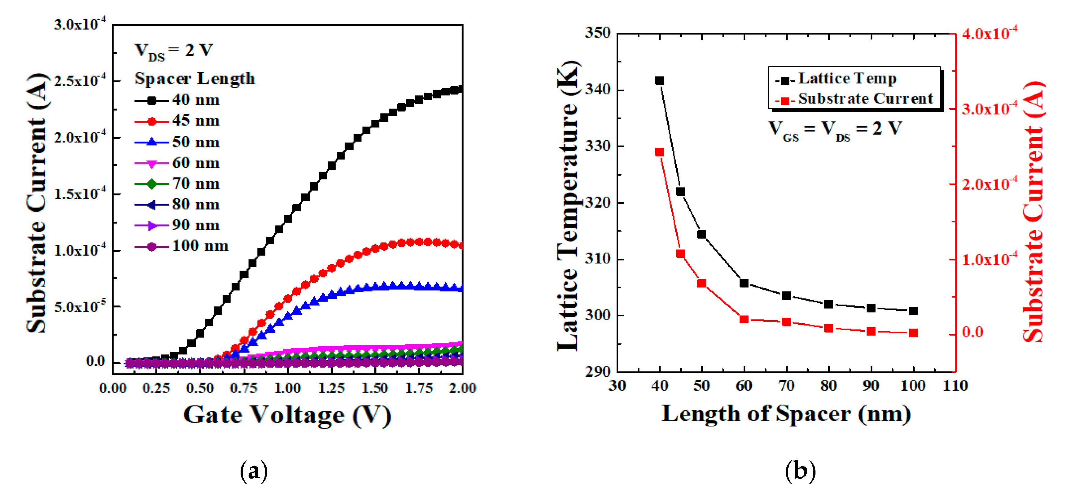
The degree of device damage due to hot carriers is generally analyzed in terms of the substrate current. Figure 4a shows the substrate current according to the spacer-length change. When the spacer length shortens below 60 nm, the substrate current increases rapidly because of impact ionization. The hot carriers generated by impact ionization further accelerate the deterioration of the device by increasing the lattice temperature. Figure 4b shows the correlation between the substrate current and lattice temperature, according to the spacer-length change. The mechanism behind SHE is the impact ionization that occurs at the junction between the P-doped and N-doped regions.
If a positive bias is applied to the n-doped region (i.e., drain region), the energy band in the N-type material will be lower than that in the steady state. On applying a more positive bias, the energy band in the N-type region will be lower [17]. An increased bias attracts electrons, which are minority carriers in the P-type region. Such carriers are accelerated by the positive bias, and the incoming electrons will collide with the other ions. Thus, they will create an electron-hole pair (EHP). The holes generated at this time pass through the substrate and partly flow to the gate to form the gate current. Therefore, when the impact ionization increases, the substrate current will increase.
3.3. Hot-Carrier Degradation
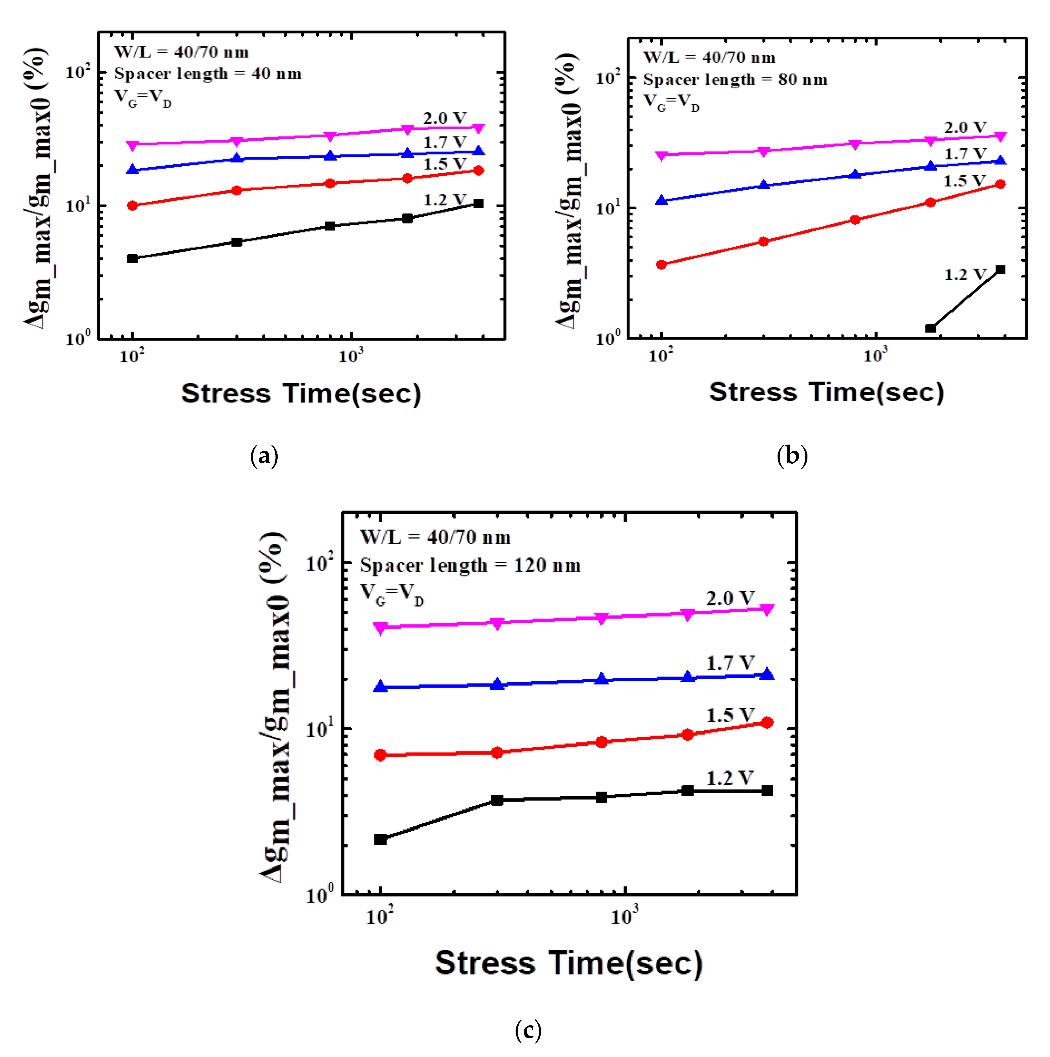
Figure 5 shows a graph of the change in transconductance over time after channel hot-electron injection into real FinFET devices with different spacer lengths. A voltage ranging from 1.2 V to −2.0 V was applied between the drain and source, and the same gate voltage was applied. The stress application time was increased from 100 s to 3800 s. When the spacer length is small, the transconductance deteriorates significantly at a small drain voltage. As the spacer length increases, the deterioration also increases at large drain voltages. As observed previously, even at low drain voltages, when the spacer length is 40 nm, impact ionization occurs because of the effect of a large electric field. Thus, a very fast deterioration rate is observed. However, if a high drain voltage is applied, deterioration due to impact ionization occurs even in a FinFET with 100-nm spacer length. In addition, it can be interpreted that more deterioration occurs at high voltages because the electron interface trap area widens.
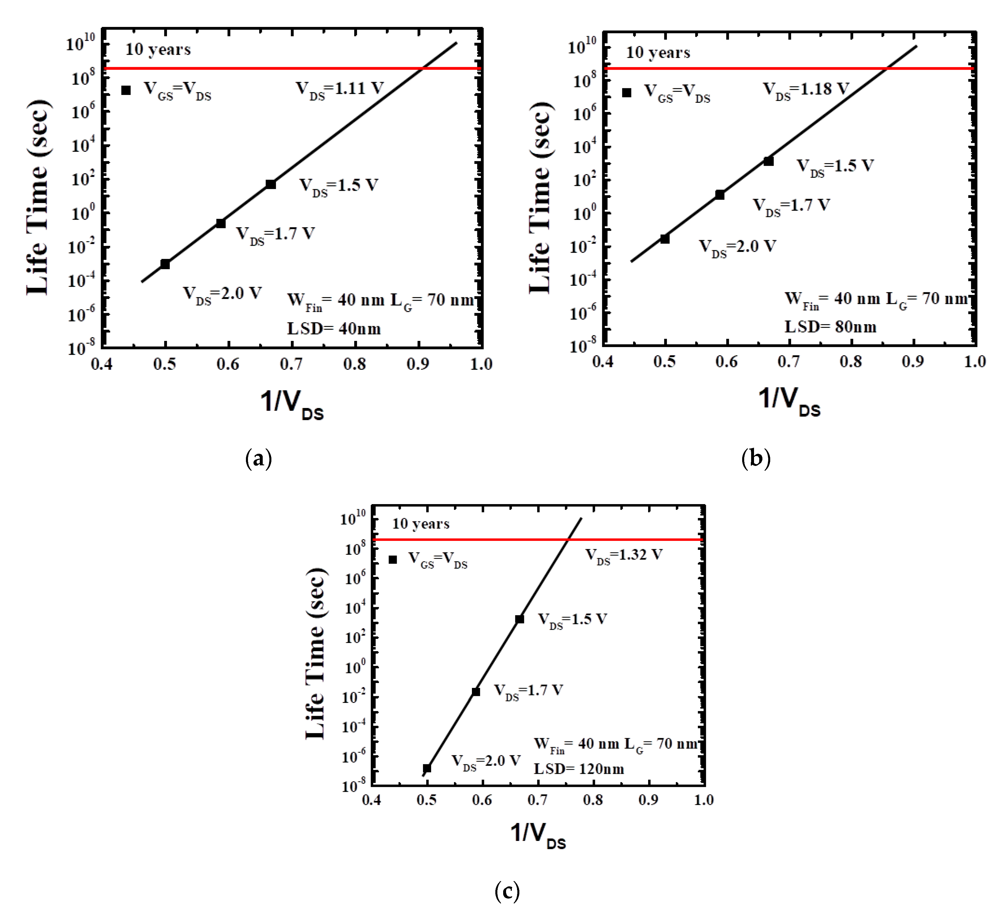
This trend is clearly presented in Figure 6, which shows the lifetime of the devices with HCE degradation. We consider the lifetime as the time at which the device shows 10% transconductance degradation. The supply voltage which meets the 10-year lifetime condition at a spacer length of 40 nm is 1.11 V; that for a spacer length of 80 nm is 1.18 V; and that for a spacer length of 120 nm is 1.32 V. As a result of this experiment, it is confirmed that, the shorter is the spacer, the easier is the deterioration, even at low drain voltages. However, this increase is very small when compared to the increase in the driving voltage required to achieve a similar performance when the spacer length is increased; thus, the effective life is expected to decrease.
4. Conclusions
According to Moore’s Law, the channel length of the transistor is reducing continuously; however, due to problems such as deterioration of the subthreshold characteristics of the transistor as a result of the deepening of the SCE, it is no longer possible to expect an improvement in performance because of a reduction in device size. To improve the performance of the transistor, a device having a 3D gate structure in which a transistor structure is changed, rather than simply scaling the channel length, was developed.
In this study, it was confirmed that the characteristics such as on/off ratio, DIBL, and SS were improved through optimization of the FinFET spacer structure. In addition, an operating voltage that could maintain a life of 10 years or more under hot-carrier injection conditions was extracted. As could be seen from the results, structural optimization was required to increase the drive current of the FinFET and prevent degradation of the analog performance.
Author Contributions
Conceptualization, J.P.; methodology, J.P. and J.K.; software, J.P.; resources, J.P. and C.S.; writing—original draft preparation, J.P.; writing—review and editing, J.P., S.S., E.-C.C., and J.Y.; supervision, E.-C.C, and J.Y.; and funding acquisition, M.S.Y. and H.R. All authors have read and agreed to the published version of the manuscript.
Funding
This work was supported by Korea Institute for Advancement of Technology (No. P0012453) and Samsung Electronics (No. s-2019-2141-026).
Acknowledgments
This research was funded and conducted under 「the Competency Development Program for Industry Specialists」 of the Korean Ministry of Trade, Industry and Energy (MOTIE), operated by Korea Institute for Advancement of Technology (KIAT). (No. P0012453, Next-generation Display Expert Training Project for Innovation Process and Equipment, Materials Engineers).
Conflicts of Interest
The authors declare no conflict of interest.
References
- Bohr, M. The evolution of scaling from the homogeneous era to the heterogeneous era. In Proceedings of the Technical Digest—International Electron Devices Meeting, Washington, DC, USA, 5–7 December 2011. [Google Scholar]
- Davari, B.; Dennard, R.H.; Shahidi, G.G. CMOS scaling for high performance and low power—The next ten years. Proc. IEEE 1995, 83, 595–606. [Google Scholar] [CrossRef] [Green Version]
- Taur, Y.; Mii, Y.J.; Frank, D.J.; Wong, H.S.; Buchanan, D.A.; Wind, S.J.; Rishton, S.A.; Sai-Halasz, G.A.; Nowak, E.J. CMOS scaling into the 21st century: 0.1 μm and beyond. IBM J. Res. Dev. 1995, 39, 245–260. [Google Scholar] [CrossRef]
- Troutman, R.R.; Chakravarti, S.N. subthreshold characteristics of insulated-gate field-effect transistors. IEEE Trans. Circuit Theory 1973, 20, 659–665. [Google Scholar] [CrossRef]
- Troutman, R.R. Subthreshold design considerations for insulated gate field-effect transistors. IEEE J. Solid-State Circuits 1974, 9, 55–60. [Google Scholar] [CrossRef]
- Troutman, R.R.; Fortino, A.G. Simple model for threshold voltage in a short-channel IGFET. IEEE Trans. Electron Devices 1977, 24, 1266–1268. [Google Scholar] [CrossRef]
- Taylor, G.W. Subthreshold conduction in mosfet’s. IEEE Trans. Electron Devices 1978, 25, 337–350. [Google Scholar] [CrossRef]
- Troutman, R.R. VLSI limitations from drain-induced barrier lowering. IEEE Trans. Electron Devices 1979, 26, 461–469. [Google Scholar] [CrossRef]
- Dennard, R.H.; Gaensslen, F.H.; Walker, E.J.; Cook, P.W. 1 µm MOSFET VLSI technology: Part 11—Device designs and characteristics for high-performance logic applications. IEEE Trans. Electron Devices 1979, 26, 325–333. [Google Scholar] [CrossRef]
- Woo, J.C.S.; Plummer, J.D. Short-channel effects in mosfet’s at liquid-nitrogen temperature. IEEE Trans. Electron Devices 1986, 33, 1012–1019. [Google Scholar] [CrossRef]
- Chamberlain, S.G.; Ramanan, S. Drain-induced barrier-lowering analysis in vsli mosfet devices using two-dimensional numerical simulations. IEEE Trans. Electron Devices 1986, 33, 1745–1753. [Google Scholar] [CrossRef]
- Fossum, J.G.; Chowdhury, M.M.; Trivedi, V.P.; King, T.J.; Choi, Y.K.; An, J.; Yu, B. physical insights on design and modeling of nanoscale FinFETs. In Proceedings of the Technical Digest—International Electron Devices Meeting, Washington, DC, USA, 8–10 December 2003; pp. 679–682. [Google Scholar]
- Trivedi, V.; Fossum, J.G.; Chowdhury, M.M. Nanoscale FinFETs with gate-source/drain underlap. IEEE Trans. Electron Devices 2005, 52, 56–62. [Google Scholar] [CrossRef]
- Cho, M.; Roussel, P.; Kaczer, B.; Degraeve, R.; Franco, J.; Aoulaiche, M.; Chiarella, T.; Kauerauf, T.; Horiguchi, N.; Groeseneken, G. Channel hot carrier degradation mechanism in long/short channel n-FinFETs. IEEE Trans. Electron Devices 2013, 60, 4002–4007. [Google Scholar] [CrossRef]
- Young, C.D.; Akarvardar, K.; Baykan, M.O.; Matthews, K.; Ok, I.; Ngai, T.; Ang, K.W.; Pater, J.; Smith, C.E.; Hussain, M.M.; et al. (110) and (100) Sidewall-oriented FinFETs: A performance and reliability investigation. Solid State Electron. 2012, 78, 2–10. [Google Scholar] [CrossRef]
- Ma, C.; Wang, H.; Zhang, C.; Zhang, X.; He, J.; Zhang, X. Temperature dependence of the interface state distribution due to hot carrier effect in FinFET device. Microelectron. Reliab. 2010, 50, 1077–1080. [Google Scholar] [CrossRef]
- Beale, J.R.A. Solid state electronic devices. Phys. Bull. 1973, 24, 178. [Google Scholar] [CrossRef]
Figure 1.
(a) Top-view SEM image of the bulk FinFET; and (b) definition of fin height, fin width, channel length, and pitch in FinFETs.
Figure 1.
(a) Top-view SEM image of the bulk FinFET; and (b) definition of fin height, fin width, channel length, and pitch in FinFETs.

Figure 2.
(a) Transfer curve; and (b) on/off current characteristics of N-type bulk FinFET according to spacer length.
Figure 2.
(a) Transfer curve; and (b) on/off current characteristics of N-type bulk FinFET according to spacer length.

Figure 3.
Drain-induced barrier lowering and sub-threshold slope characteristics comparison of N-type bulk FinFET according to spacer length.
Figure 3.
Drain-induced barrier lowering and sub-threshold slope characteristics comparison of N-type bulk FinFET according to spacer length.

Figure 4.
(a) Substrate current versus gate voltage characteristics; and (b) comparison of substrate current and lattice temperature of N-type bulk FinFET according to spacer length.
Figure 4.
(a) Substrate current versus gate voltage characteristics; and (b) comparison of substrate current and lattice temperature of N-type bulk FinFET according to spacer length.

Figure 5.
Transconductance degradation for different spacer lengths under the stress conditions of: (a) LSD = 40 nm; (b) LSD = 80 nm; and (c) LSD = 120 nm.
Figure 5.
Transconductance degradation for different spacer lengths under the stress conditions of: (a) LSD = 40 nm; (b) LSD = 80 nm; and (c) LSD = 120 nm.

Figure 6.
Device lifetime for different stress bias conditions with different spacer lengths under the stress conditions obtained by extrapolation with Figure 5 of: (a) LSD = 40 nm; (b) LSD = 80 nm; and (c) LSD = 120 nm.
Figure 6.
Device lifetime for different stress bias conditions with different spacer lengths under the stress conditions obtained by extrapolation with Figure 5 of: (a) LSD = 40 nm; (b) LSD = 80 nm; and (c) LSD = 120 nm.


Table 1.
Device structure parameters of FinFETs.
| Device Parameters | Value |
|---|---|
| Gate length (L) | 70 nm |
| Fin width (Wfin) | 40 nm |
| Fin height (Hfin) | 30 nm |
| Number of fins | 5 |
| Fin pitch | 200 nm |
| Spacer length (LSD) | 40~100 nm |
Table 2.
Electrical properties of bulk FinFET according to spacer length.
| LSD (nm) | On/Off Ration | DIBL (mV/V) | SS (mV/dec) |
|---|---|---|---|
| 40 | 3.18 × 10⁵ | 130.70 | 107.24 |
| 50 | 2.67 × 10⁶ | 78.19 | 78.08 |
| 60 | 3.20 × 10⁷ | 36.40 | 70.17 |
| 70 | 6.91 × 10⁷ | 19.47 | 67.30 |
| 80 | 7.73 × 10⁷ | 18.68 | 64.79 |
| 90 | 6.05 × 10⁷ | 18.41 | 64.29 |
| 100 | 3.88 × 10⁷ | 17.64 | 66.82 |
© 2020 by the authors. Licensee MDPI, Basel, Switzerland. This article is an open access article distributed under the terms and conditions of the Creative Commons Attribution (CC BY) license (http://creativecommons.org/licenses/by/4.0/).
Share and Cite
MDPI and ACS Style
Park, J.; Kim, J.; Showdhury, S.; Shin, C.; Rhee, H.; Yeo, M.S.; Cho, E.-C.; Yi, J. Electrical Characteristics of Bulk FinFET According to Spacer Length. Electronics 2020, 9, 1283. https://doi.org/10.3390/electronics9081283
AMA Style
Park J, Kim J, Showdhury S, Shin C, Rhee H, Yeo MS, Cho E-C, Yi J. Electrical Characteristics of Bulk FinFET According to Spacer Length. Electronics. 2020; 9(8):1283. https://doi.org/10.3390/electronics9081283
Chicago/Turabian StylePark, Jinsu, Jaemin Kim, Sanchari Showdhury, Changhwan Shin, Hwasung Rhee, Myung Soo Yeo, Eun-Chel Cho, and Junsin Yi. 2020. "Electrical Characteristics of Bulk FinFET According to Spacer Length" Electronics 9, no. 8: 1283. https://doi.org/10.3390/electronics9081283
Note that from the first issue of 2016, this journal uses article numbers instead of page numbers. See further details here.