Article

Direct Space Vector Modulation with Novel DC-Link Voltage Balancing Algorithm for Easy Software Implementation of Three-Phase Three-Level Converter

1
Center for Intelligent and Interactive Robotics, Korea Institute of Science and Technology, Seoul 02792, Korea
2
Department of Electrical Engineering, Hanbat University, Daejeon 305-719, Korea
*
Author to whom correspondence should be addressed.
Electronics 2020, 9(11), 1841; https://doi.org/10.3390/electronics9111841
Submission received: 28 September 2020 / Revised: 22 October 2020 / Accepted: 26 October 2020 / Published: 3 November 2020
(This article belongs to the Special Issue Design and Optimization of High-Frequency Power Converter)

Abstract

:
The present paper proposes a direct space vector modulation and novel balance algorithm for easy software application of three-level converters which operate in three-phase. In the case of the conventional space vector modulation, to get the on-state times of the switches, the dwell times of the three nearest stationary vectors, which are obtained after sector and region selection algorithms, should be rearranged. These processes, therefore, contain diverse conditional statements and complicated calculations such as inverse trigonometric functions and square roots. However, the burden of the software application of the proposed algorithm is greatly reduced by not using the sector selection algorithm, the region selection algorithm, and the on-state time allocation process as the proposed modulation can directly control the switch on-state time. In a three-level topology, it is required to balance top and bottom capacitor voltages because the DC-link voltage is composed of two capacitor voltages; the unbalanced voltage of each DC-link capacitor causes the overvoltage of the switching devices. Thus, the DC-link voltage balancing algorithm is proposed, and it is also very simple and effective without additional circuits because it controls the switch on-state time directly as well. The 5-kW prototype proved the validity of the proposed algorithm with its feasibility.

1. Introduction

For three-phase control, space vector modulation (SVM) control is commonly used [1,2]. The SVM is useful because, at the same carrier frequency, the switching number is about 30% less and the maximum possible output voltage is 15.5% higher than the sinusoidal pulse width modulation method [3]. The current controller in the dq frame gives the angle of desired vector and magnitude to SVM algorithm; the dq frame is often used to regulate the reactive power and active power [4,5]. However, in this procedure, the SVM demands complex calculations such as the inverse trigonometric functions and the square root of the microprocessor [6]. Moreover, a three-level converter requires much more complex selection algorithms than a two-level converter to control through the SVM; a three-level converter has at least six sectors, each of which is separated into a chain of regions [7,8]. Furthermore, at the end of the selection algorithm, the dwell time of the vectors should be properly distributed to the switch on-state time [9].
Under the same input/output state with the same filter size, three-level converters have better power conversion efficiency, rated voltage conditions, and current total harmonic distortion (THD) compared to two-level converters [10]. However, three-level converters require two DC-link capacitors linked in series to produce different voltage levels, unlike conventional two-level converters. Therefore, the DC-link voltage could be unbalanced, which causes overvoltage of the switching device and high THD of the grid current, so the two DC-link voltages should be controlled to be the same [11,12]. While additional circuits may solve this balancing problem, this solution increases power loss, cost, and complexity of the circuit [13,14,15].
In this study, the proposed algorithm and DC-link voltage balancing algorithm were validated through the T-type topology which represents the three-level converter. The proposed direct space vector modulation (DSVM) controls the switch on-state time directly without complicated calculations such as sector and region selection algorithms and on-state time allocation procedure on the software. In addition, the balancing algorithm that uses DSVM not only reduces the load of the software, but also eliminates the need for additional circuit configuration; its principle includes the direction of neutral current and its magnitude. The DC-link voltage comes into a balanced state by controlling the neutral-point-current, so the concerns about overvoltage on switching devices are reduced. The final switch on-state time is the sum of the compensated on-state time and on-state time, which is calculated from DSVM. This paper carries out the analysis of the conventional SVM and the theoretical analysis of the proposed DSVM and DC-link voltage balancing algorithms. Then, the experimental results of the 5-kW T-type topology prototype are provided to verify the validity of the proposed algorithm with its feasibility.

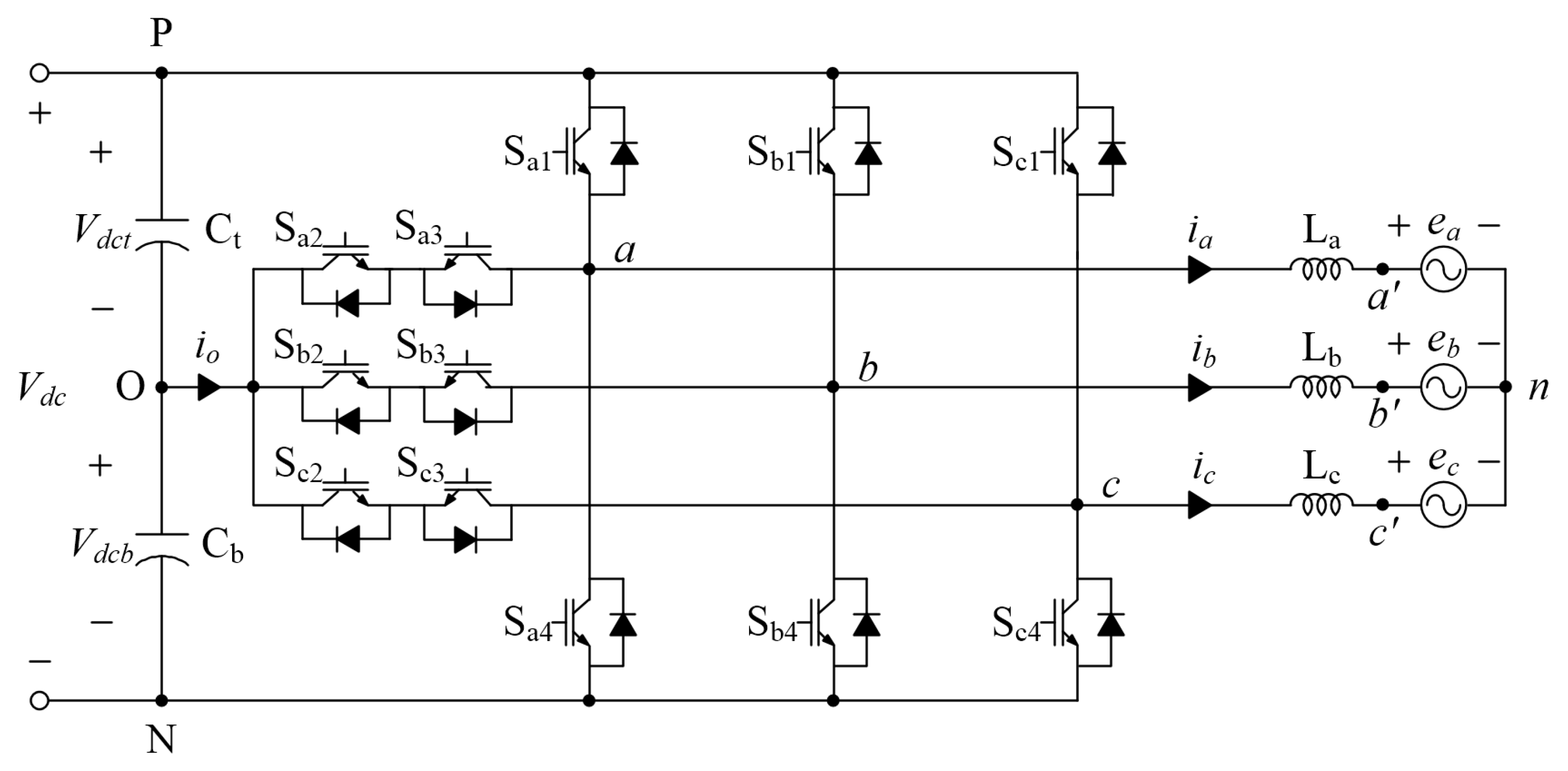
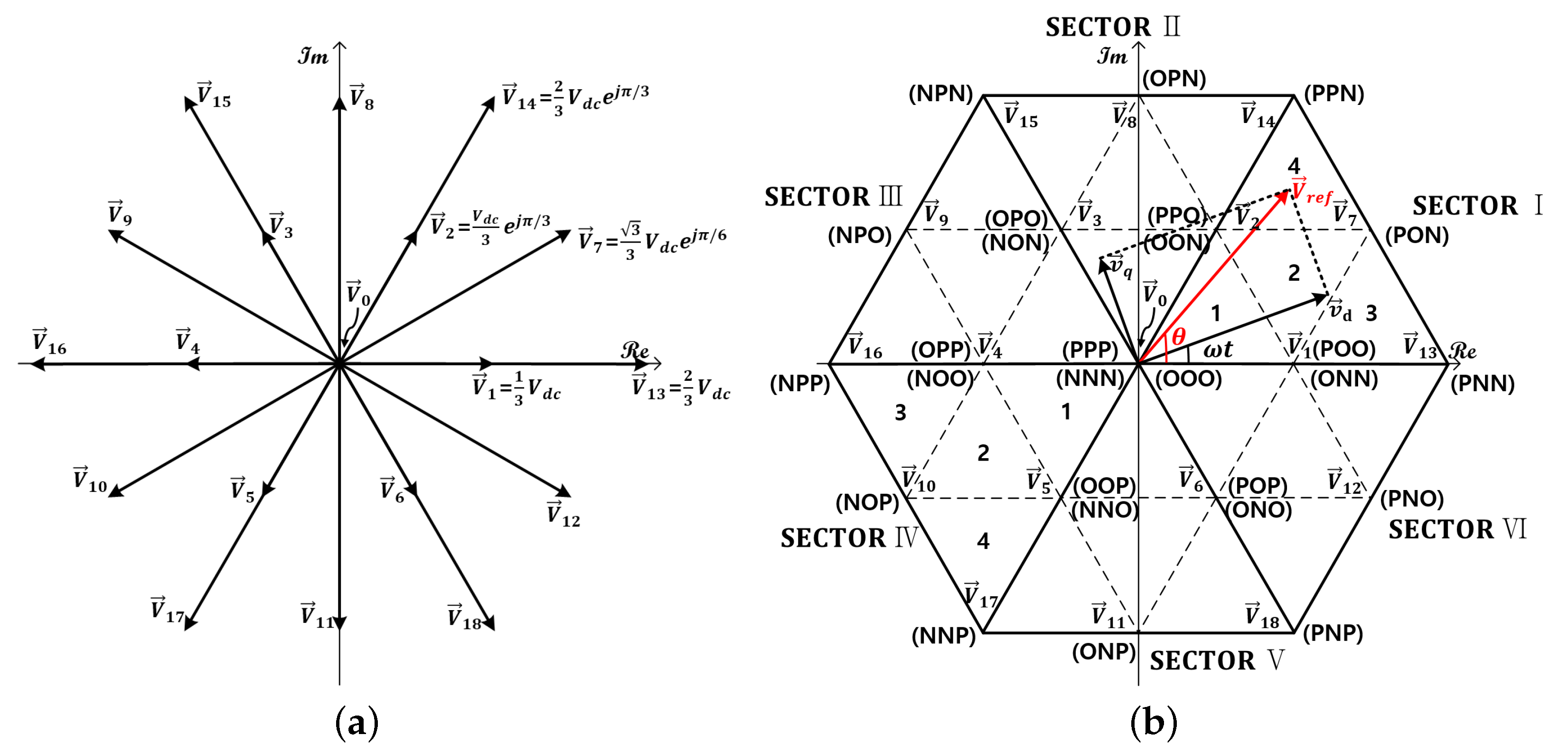
2. Algorithm Analysis

As shown in Figure 1, the grid voltages are e a , e b , and e c ; the grid currents are i a , i b , and i c ; and the branch voltages are v a n , v b n , and v c n . In the stationary, abc frame, the voltage equations are as follows:
e a = E c o s ω t = L d i a d t + v a n e b = E c o s ω t 2 3 π = L d i b d t + v b n e c = E c o s ω t 4 3 π = L d i c d t + v c n ,
where E and ω are the grid voltage amplitude and the angular frequency of the grid voltage. L a , L b , and L c , which are filter inductors, have the same value of inductance L. The voltage equations in (1) are transformed from abc frame to dq frame as
e d = E = L d i d d t + ω L i q + v d e q = 0 = L d i q d t ω L i d + v q ,
where d-axis grid voltage and current are e d and i d ; q-axis grid voltage and current are e q and i q ; d-axis branch voltages is v d ; and q-axis branch voltages is v q . By using (2), the active power P which is supplied to the grid is
P = 3 2 ( e d i d + e q i q ) = 3 2 E i d .
i q cannot affect the active power P of (3) because e q is 0 in (2). Therefore, the q-axis reference grid current i q * should be 0 for the zero reactive power and unity power factor.
For linear control, the following equations should be satisfied:
v d = E ω L i q + Δ v d v q = ω L i d + Δ v q ,
where the variation of d-axis branch voltage is Δ v d and the variation of q-axis branch voltage is Δ v q . They can be controlled as
Δ v d = k p d ( i d * i d ) + k i d ( i d * i d ) d t Δ v q = k p q ( i q * i q ) + k i q ( i q * i q ) d t ,
where the proportional control gains of Δ v d is k p d ; the proportional control gains of Δ v q is k p q ; the integral control gains of Δ v d is k i d ; and the integral control gains of Δ v q is k i q . Since the current controller provides the branch voltages as (4), Equation (2) is easy to control as below:
L d i d d t + Δ v d = 0 L d i q d t + Δ v q = 0 .
This directly controls the grid current and could improve the power quality with simple control.

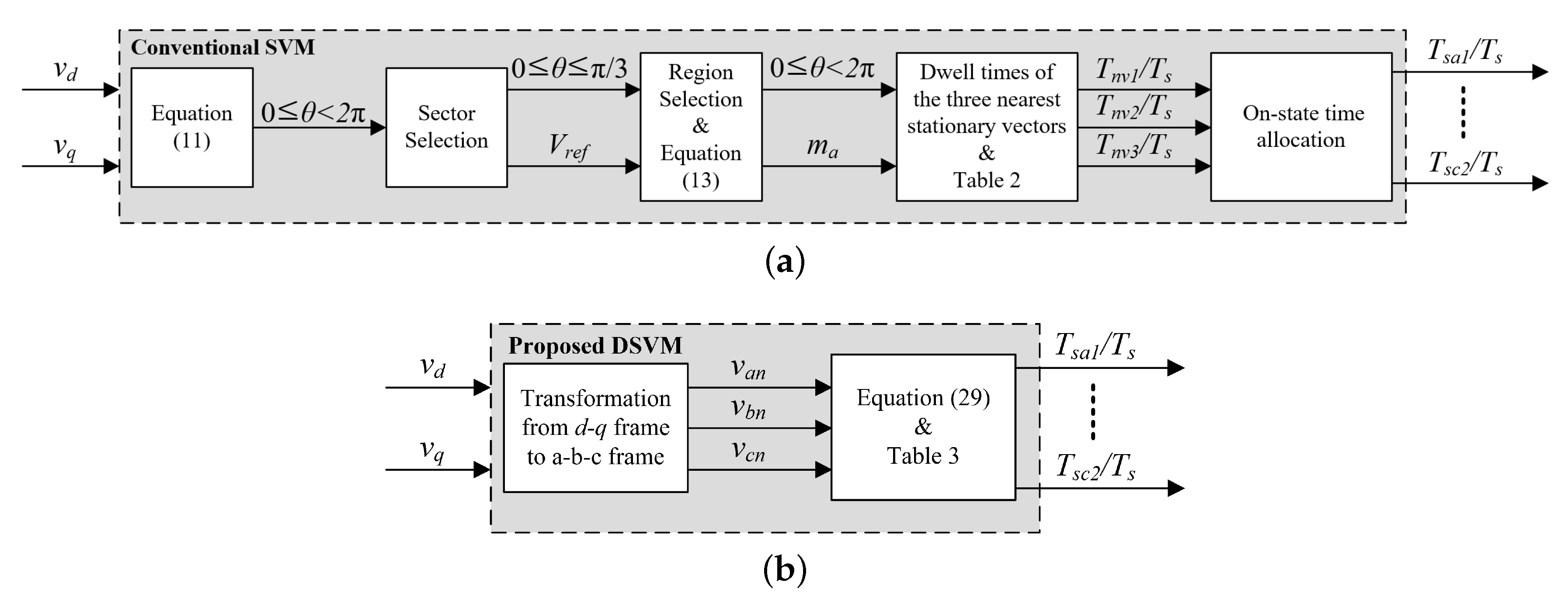
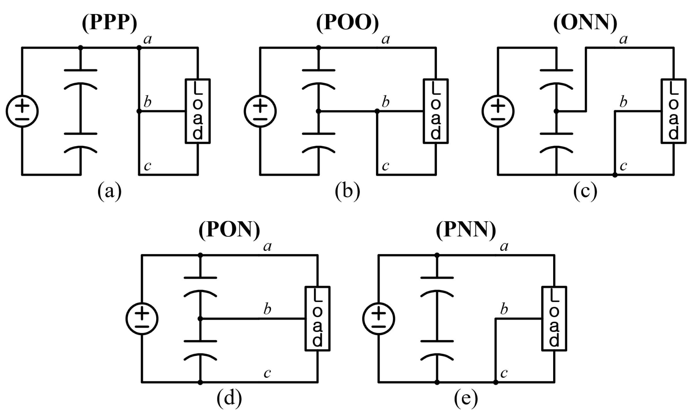
2.1. The Conventional SVM Algorithm

The conventional SVM is a switching modulation technique for the three-phase current control of converters. In this modulation, the branch voltages of (4) are considered as the desired voltage. A three-level cell has three switching states, as presented in Table 1, because S x 2 and S x 4 (x = a , b , c ) operate in complementary relations similar to S x 1 and S x 3 . Thus, the three-level converter which operates in three-phase has 27 (= 3 × 3 × 3) switching states because of the three legs configuration.
In a complex plane, v a n , v b n , and v c n , which are three branch voltages, can be represented as a single variable by utilizing the space vector transformation. The space vector u ( t ) in complex plane can be expressed as
u ( t ) = 2 3 u a ( t ) + u b ( t ) e j 2 3 π + u c ( t ) e j 2 3 π ,
where a scaling factor is 2 3 . Any three of time functions which fulfill u a ( t ) + u b ( t ) + u c ( t ) = 0 could be expressed in two-dimensional space. Thus, 27 space vectors with 19 values of vectors ( V 0 V 18 ) could be drawn in complex planes, as shown in Figure 2a, and the 27 space vectors are classified into four groups: small, medium, large, and zero. In addition, in accordance with Figure 2b, the vector space can be six triangular sectors (I–VI); each triangular sector can be further divided into four triangular regions (1–4). The reference space vector V r e f of Figure 2b is provided from (4), and this reference space vector V r e f can be redefined by the three nearest stationary vectors. For example, if V r e f is in Region 4 of SECTOR I as in Figure 2b, V 2 , V 7 , and V 14 are the three nearest stationary vectors:
V 2 T n v 1 + V 7 T n v 2 + V 14 T n v 3 = V r e f T s
T n v 1 + T n v 2 + T n v 3 = T s ,
where, in this case, the dwell times of V 2 , V 7 , and V 14 are T n v 1 , T n v 2 , and T n v 3 , respectively. The switching period is T s . In addition, the three nearest stationary vectors V 2 , V 7 , and V 14 are represented as
V 2 = 1 3 V d c e j 1 3 π V 7 = 3 3 V d c e j 1 6 π V 14 = 2 3 V d c e j 1 3 π V r e f = V r e f e j θ ,
where
V r e f = v d 2 + v q 2 , θ = ω t + t a n 1 v q v d .
After putting (10) into (8), the equation could be split into the real part and the imaginary part. Then, by utilizing (9), the dwell times are obtained as
T n v 1 = T s 2 2 m a s i n π 3 + θ T n v 2 = T s 2 m a s i n π 3 θ T n v 3 = T s [ 2 m a s i n θ 1 ] ,
where the modulation index is m a , which is defined as
m a = 3 V r e f V d c 0 m a 1 .
The above processes could be repeated for each region. Consequently, Table 2 is the calculation results of the space vector dwell times for the V r e f in SECTOR I. For the other sectors (II–VI) of dwell times for V r e f , the results of Table 2 can be utilized; if the integer multiple of π /3 is taken from the actual angular displacement θ , the calculation results are available because the changed angle is in between 0 and π /3.

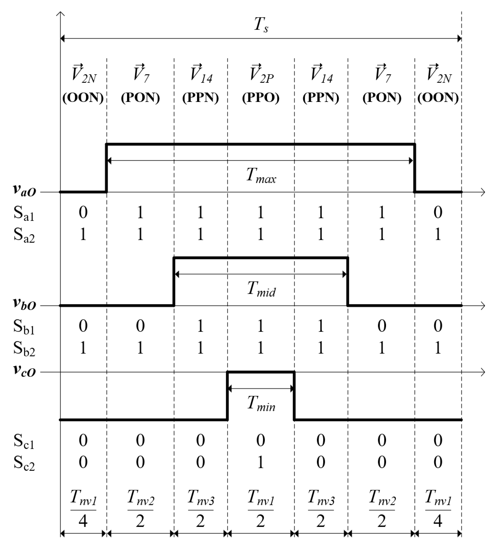
2.2. The Proposed DSVM Algorithm

Because S x 2 and S x 4 operate in complementary relations, as indicated in Section 2.1, the S x 4 on-state time can be represented as T s T s x 2 where T s x 2 is the on-state time of S x 2 and T s x 4 is the on-state time of S x 4 (x = a , b , c ). Thus, v a O , v b O , and v c O , which are the terminal voltages, are represented as
v a O = T s a 1 T s V d c 2 + T s T s a 2 T s V d c 2 v b O = T s b 1 T s V d c 2 + T s T s b 2 T s V d c 2 v c O = T s c 1 T s V d c 2 + T s T s c 2 T s V d c 2 .
In addition, they can be represented as
v a O = v a n + v n O v b O = v b n + v n O v c O = v c n + v n O .
From (15), v n O is given as
v a O + v b O + v c O = v a n + v b n + v c n + 3 v n O
v n O = v a O + v b O + v c O 3 ( v a n + v b n + v c n = 0 ) .
Therefore, from (14), (15), and (17), v a n , v b n , and v c n are arranged as
v a n = V d c 6 T s [ 2 ( T s a 1 + T s a 2 ) ( T s b 1 + T s b 2 ) ( T s c 1 + T s c 2 ) ] v b n = V d c 6 T s [ ( T s a 1 + T s a 2 ) + 2 ( T s b 1 + T s b 2 ) ( T s c 1 + T s c 2 ) ] v c n = V d c 6 T s [ ( T s a 1 + T s a 2 ) ( T s b 1 + T s b 2 ) + 2 ( T s c 1 + T s c 2 ) ] .
In matrix form, (18) is arranged as
v a n v b n v c n = V d c 6 T s 2 1 1 1 2 1 1 1 2 T s a 1 + T s a 2 T s b 1 + T s b 2 T s c 1 + T s c 2 .
As shown in Figure 2b, if V r e f is in Region 4, which is in SECTOR I, the three nearest vectors are V 2 , V 7 , and V 14 . In addition, because small vectors have P- and N-type, ( V 2 P , V 7 , and V 14 ), ( V 2 N , V 7 , and V 14 ), or ( V 2 P , V 2 N , V 7 , and V 14 ) can be utilized for V r e f . If V r e f is computed by a P-type space vector V 2 P (PPO) with V 7 (PON) and V 14 (PPN), the switch on-state time and the space vector dwell time are represented as
T s a 1 T s a 2 T s b 1 T s b 2 T s c 1 T s c 2 = T n v 1 T n v 1 T n v 1 T n v 1 0 T n v 1 + T n v 2 T n v 2 0 T n v 2 0 0 + T n v 3 T n v 3 T n v 3 T n v 3 0 0 .
Because of T s a 1 = T s a 2 = T s , v a O is V d c / 2 from (9), (14), and (20). Therefore, from (14), T s a 1 + T s a 2 , T s b 1 + T s b 2 , T s c 1 + T s c 2 are obtained as
T s a 1 + T s a 2 T s b 1 + T s b 2 T s c 1 + T s c 2 = 2 T s T s T s 2 T s V d c V d c / 2 v a O V d c / 2 v b O V d c / 2 v c O
= 2 T s T s T s 2 T s V d c v a O v a O v a O v b O v a O v c O
= 2 T s T s T s 2 T s V d c v a n v a n v a n v b n v a n v c n
= 2 T s T s T s 2 T s V d c v m a x v a n v m a x v b n v m a x v c n ,
where v m a x (=max( v a n , v b n , v c n )) is the maximum branch voltage; the branch voltage can be maximized by the maximum value of T s x 1 + T s x 2 (x = a , b , c ) because of (19). Thus, because of T s a 1 = T s a 2 = T s from (9) and (20), v a n is v m a x .
If V r e f is computed by the N-type space vector V 2 N (OON) with V 7 (PON) and V 14 (PPN) instead of V 2 P (PPO), the switch on-state times and the space vector dwell time is obtained as
T s a 1 T s a 2 T s b 1 T s b 2 T s c 1 T s c 2 = 0 T n v 1 0 T n v 1 0 0 + T n v 2 T n v 2 0 T n v 2 0 0 + T n v 3 T n v 3 T n v 3 T n v 3 0 0 .
Because of T s c 1 = T s c 2 = 0, V d c / 2 is v c O from (14) and (25). Therefore, after the same process as the above procedures of (21)–(24), T s a 1 + T s a 2 , T s b 1 + T s b 2 , and T s c 1 + T s c 2 are represented as
T s a 1 + T s a 2 T s b 1 + T s b 2 T s c 1 + T s c 2 = 2 T s V d c v a O + V d c / 2 v b O + V d c / 2 v c O + V d c / 2
= 2 T s V d c v a n v m i n v b n v m i n v c n v m i n ,
where v m i n (=min( v a n , v b n , v c n )) is the minimum branch voltage. For the minimum deviation of the DC-link voltages, the P-type state and the N-type state in the dwell time of V 2 should be equal during T s ideally. Therefore, from (20) and (25), if V 2 P and V 2 N are utilized equally during T s , the space vector dwell time and the switch on-state time are obtained as
T s a 1 T s a 2 T s b 1 T s b 2 T s c 1 T s c 2 = T n v 1 / 2 T n v 1 T n v 1 / 2 T n v 1 0 T n v 1 / 2 + T n v 2 T n v 2 0 T n v 2 0 0 + T n v 3 T n v 3 T n v 3 T n v 3 0 0 .
T s a 1 + T s a 2 , T s b 1 + T s b 2 , and T s c 1 + T s c 2 , from (24) and (27), are represented as
T s a 1 + T s a 2 T s b 1 + T s b 2 T s c 1 + T s c 2 = T s T s T s + T s V d c v a n v m i n v b n v m i n v c n v m i n T s V d c v m a x v a n v m a x v b n v m a x v c n .
The switch on-state times are calculated as represented in Table 3 thanks to the switching characteristics of three-level in [16]. Therefore, the proposed DSVM directly provides the switch on-state times from (29) without complicated computations, i.e. square root, inverse trigonometric function, sector and region selection algorithms, and on-time allocation process. As shown in Figure 3, DSVM takes the switch on-state time more easily through the greatly simplified procedures than the conventional SVM; DSVM needs just one generalized equations, whereas many conditional statements should be included in each block diagram of the conventional SVM in Figure 3. In accordance with Table 4, there are huge differences in complexity of switching sequences for DSVM compared to other methods. Even if, in [11], the number of switching sequence is zero, each sectors has the different equations for the switch on-state time. However, in DSVM, only one generalized equation covers all sectors, and the proposed DSVM can calculate the switch on-state time without considering of the switching sequence, sectors, and regions.

2.3. The Proposed Balancing Algorithm of the DC-Link Voltage

A seven-segment switching sequence is used for the three-level converter which operates in three-phase after DSVM. Its characteristics could be summarized as follows: (A) T s is composed of seven segments of the dwell times for the three stationary space vectors which are the nearest to the reference. (B) The three space vectors have four switching states since the P-type state and the N-type state in the dwell time of small vectors should be equal during T s for the minimum deviation of the DC-link voltages. (C) The change to the another segment is only one leg switching state. The change in Figure 4, for example, from the (PPN) to the (PPO) is conducted by altering the c-terminal side leg switching state from (N) to (O). (D) For the grid current THD, the segment sequences are center-aligned and symmetric. (E) The center segment, which is the P-type vector switching state, and the edge segments, which are the N-type vector switching state, have the same dwell time.
The switching state sequence based on (A)–(E) for V r e f is shown in Figure 4. As referred to (C) and (E), the movement from the edge to the center make the switching states of all three legs change. Therefore, In Table 3 and Figure 4, if S x 1 (or S x 2 ) is 1 or 0 continuously during T s , the other switch S x 2 (or S x 1 ) is one of T m a x , T m i d , and T m i n ; T m a x is the five centered segments period; T m i d is the three centered segments period; and T m i n is the centered segment period. Thus, by utilizing (E),
T s = T m a x + T m i n .
As shown in Figure 5, the five states of the space vectors are (PPP) of a zero vector, (POO) and (ONN) of two small vectors, (PON) of a medium vector, and (PNN) of a large vector. Although Figure 5 represents only the state of (PPP), the converter operates in zero vector V 0 with (PPP), (NNN), and (OOO). In the state of (PPP), as shown in Figure 5a, the a, b, and c terminals are linked to the positive node of the DC-source because the all of S x 1 and S x 2 in three legs are turned on (x = a , b , c ). Thus, the voltage difference between the top capacitor and the bottom capacitor maintains constant since the capacitors are linked only to the DC-source. The same is true for (OOO) and (NNN). Figure 5b shows the circuit diagram of small vector V 1 P (POO); the top capacitor voltage V d c t is decreased since the neutral current i O flows in the negative direction. On the other hand, as shown in Figure 5c, the bottom capacitor voltage V d c b is decreased since i O flows out in a positive direction during (ONN) state. In other words, V d c t is elevated relatively if i O flows in the positive direction, while V d c b is increased relatively if i O flows in the negative direction. Therefore, in the case of the medium vector V 7 (PON) in Figure 5d, the voltage variation of the DC-link capacitors depends on the direction of i O . Since the current amount which flows through the DC-link capacitors is the same, the large vector V 13 (PNN) shown in Figure 5e does not affect voltage difference between the top capacitor and the bottom capacitor.
It can be assumed that the grid current is constant during T s because the switching frequency is far higher than the grid frequency. Therefore, i O , 1 s = i O , 4 s = i O , 7 s , i O , 3 s = i O , 5 s , and i O , 2 s = i O , 6 s , where the neutral current i O of each segment sequence is sorted by i O , 1 s i O , 7 s ; for example, i O , 3 s is the neutral current in the third segment of the seven segments. Thus, through utilization of (30), i O is represented as
i O = i O , 1 s ( T s T m a x ) + i O , 2 s ( T m a x T m i d ) T s + i O , 3 s ( T m i d T m i n ) + i O , 4 s T m i n T s
= i O , 2 s ( T m a x T m i d ) + i O , 3 s ( T m i d T m i n ) T s .
By using Figure 4, T m a x , T m i d , and T m i n can be obtained as
T m a x = T s a 1 T m i d = T s b 1 T m i n = T s c 2 = T s T s a 1 .
Thus, by utilizing (32) and (33),
i O = i O , 2 s ( T s a 1 T s b 1 ) T s 0 ,
where i O , 3 s =0 because i O is zero in Figure 5e. Thus, the compensated dwell time T c o m p for the balancing control can be expressed as
T c o m p = k V e r r o r + α ( , where V e r r o r = V d c t V d c b ) ,
where the proportional gain is k ( > 0 ) and the compensation value is α . If T c o m p compensates T m a x , T m i d , and T m i n equally, (31) is reorganized as below
i O , c o m p = i O , 1 s ( T s ( T m a x + T c o m p ) ) T s + i O , 2 s ( ( T m a x + T c o m p ) ( T m i d + T c o m p ) ) T s + i O , 3 s ( T m i d + T c o m p ) ( T m i n + T c o m p ) ) T s + i O , 4 s ( T m i n + T c o m p ) T s = i O + 2 i O , 4 s T c o m p T s .
To eliminate i O term, α can be expressed as:
α = i O 2 i O , 4 s T s .
Thus, from (35)–(37), the compensated neutral current i O , c o m p is expressed as:
i O , c o m p = k V e r r o r ,
where 2 i O , 4 s k / T s is k ( < 0 ) and i O , 4 s < 0 since the centered segment is the P-type small vector switching state from E). If, in DC-link unbalanced condition, V d c b is lower than V d c t ( V e r r o r > 0 ), i O , c o m p in (38) has a negative value. Thus, since i O , c o m p has a negative value, the bottom capacitor voltage V d c b relatively increases for the balance. On the other hand, if V d c b is higher than V d c t ( V e r r o r < 0 ), i O , c o m p in (38) has a positive value. Therefore, the bottom capacitor voltage V d c b relatively decreases for the balance DC-link condition. Consequently, the final switch on-state time is rearranged by adding T c o m p to the existing switch on-state time as below
T m i n , c o m p = T m i n + T c o m p T m i d , c o m p = T m i d + T c o m p T m a x , c o m p = T m a x + T c o m p .

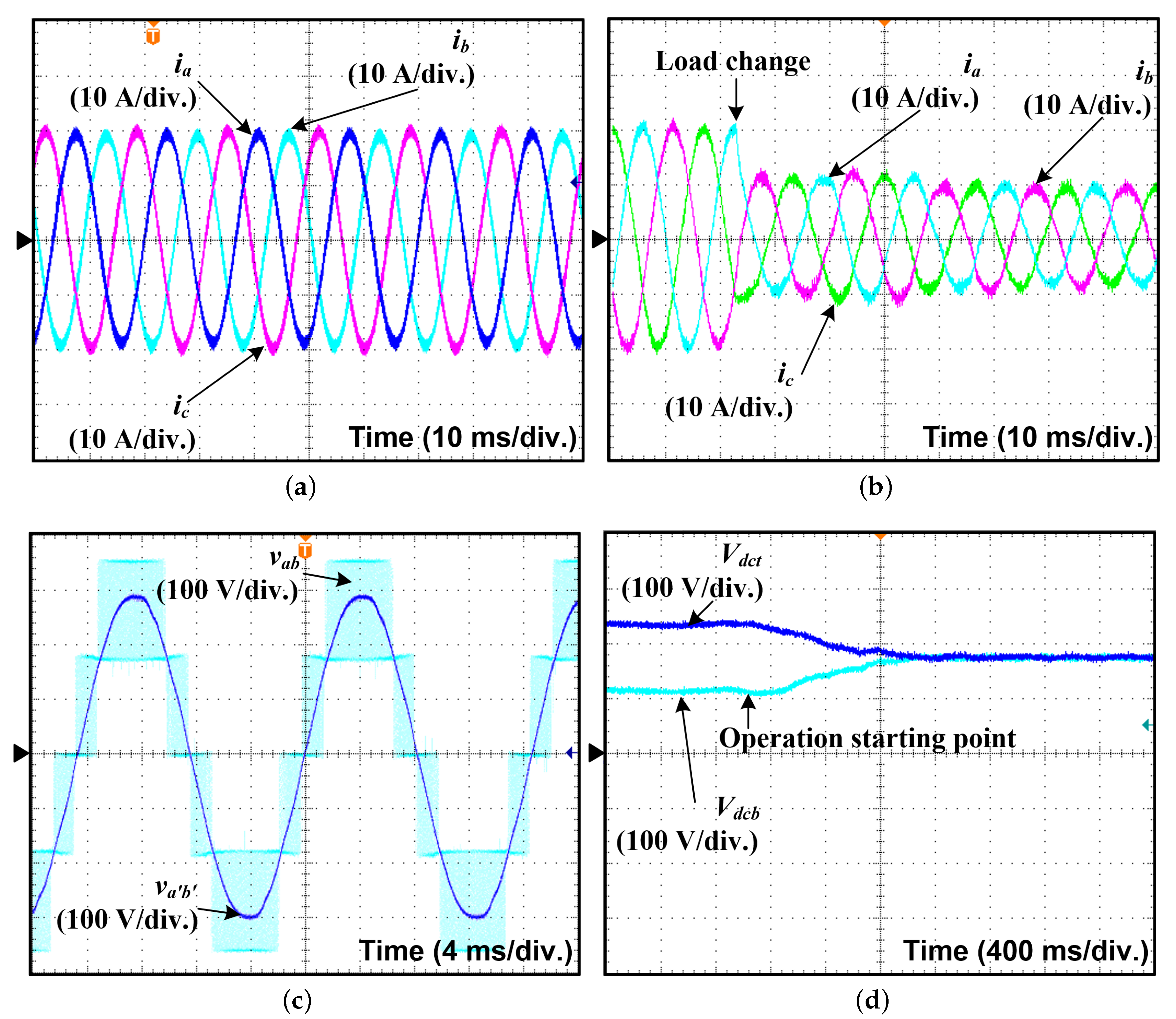
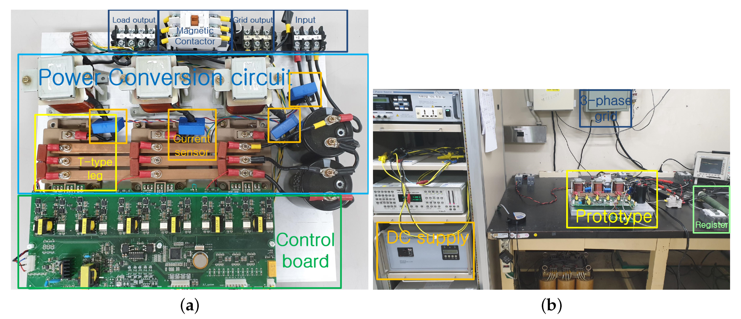
3. Experimental Result

To demonstrate the validity of DSVM and its feasibility, grid-connected experiments were conducted using the prototype for the proposed converter in Figure 1. The parts and component values of the prototype, as shown in Figure 1, are as follows: a-, b-, and c-phase T-type module, 4MBI300VG-120R-50; current sensor, LA 55-P; capacitance of C t and C b , 2200 μ F; and inductance of L a , L b , and L c , 1 mH. The DC-link voltage V d c is 360 V; the line voltage v a b is 220 V rms ; the grid frequency f g is 60 Hz; and the rated power P o is 5 kW.
Figure 6 shows the experimental results of T-type converter which operates in three-phase and utilizes the proposed control algorithms. i a , i b , and i c , which are the grid currents in Figure 6a, show sinusoidal wave form with the phase difference of 120 . In addition, they provides the desired rated power of 5 kW. Each of the grid currents is controlled very well as the sinusoidal form in Figure 6a. Furthermore, to check the response time in transient condition, load variation was conducted (Figure 6b). In this experiment, the grid currents i a , i b and i c were changed smoothly and quickly from 5 to 2.5 kW. As a result, those experiments completely demonstrated the validity of the proposed control algorithm and its feasibility. As represented in Figure 6c, the three-level voltage v a b has five voltage levels, and the line voltage v a b is the 220 V rms sine wave. To verify the proposed DC-link voltage balancing algorithm, the initial unbalancing experiment was conducted, as presented in Figure 6d, which shows the voltage of the top capacitor V d c t and the voltage of the bottom capacitor V d c b . The V d c t initial condition is 240 V and the V d c b initial condition is 120 V. To make the initial unbalanced DC-link state, the register linked to the circuit breaker, as shown in Figure 7b, is temporarily utilized before the operation. As shown in Figure 6d, after starting the operation of the converter, which conducts the proposed algorithm, the difference between V d c t and V d c b has become zero. It proves that the proposed balancing algorithm gives equal distribution of two DC-link capacitor voltages. Thus, the proposed DSVM and the balancing algorithm for the three-level converter which operates in three-phase permit giving precise current control and the DC-link capacitor voltages balancing.
Pictures of experiment environment are shown in Figure 7. The prototype is evenly arranged, as represented in Figure 7a, and a plate also acts as the heatsink and support at the same time. In addition, the power circuit and control board are insulated. As shown in Figure 7b, DC power supply gives the power for the prototype, and the prototype transfers the power to the three-phase grid. To create an initial DC-link unbalance condition, the register linked to the circuit breaker in Figure 7b is utilized temporarily before the converter operation, as shown in Figure 6d.

4. Conclusions

This paper proposes a direct space vector modulation and a novel DC-link voltage balance algorithm for easy software application of three-level converters which operate in three-phase. The proposed DSVM directly gives the switch on-state time without complicated computations, which are the on-state time allocation process and sector and region selection algorithms. Due to DSVM, a novel DC-link voltage balancing algorithm is also developed. The three-level converters have two divided DC-link capacitors which are linked in series. Then, it can generate the unbalanced voltages of the DC-link capacitors which is causing raised concerns about overvoltage on switching devices. In addition, the equal voltages of the DC-link capacitors linked in series can improve the current quality of the three-level converters. The proposed balancing algorithm with DSVM simply controls the DC-link voltages in equality by adjusting the neutral current and provides an effective balance control without the additional hardware and complex calculations. Therefore, the proposed DSVM and the balancing algorithm are simple to apply to three-level converters which operate in three-phase, and the experimental results thoroughly represent the validity, effectiveness, and feasibility of the proposed algorithms.

Author Contributions

J.-S.K. performed the experiments, analyzed the data, and mainly wrote the manuscript; J.-M.K. managed the project and edited the manuscript. All authors have read and agreed to the published version of the manuscript.

Funding

This research received no external funding.

Conflicts of Interest

The author declares no potential conflict of interest.

References

  1. Alberto, F.; Batista, B.; Barbi, I. Space Vector Modulation Applied to Three-Phase Three-Switch Two-Level Unidirectional PWM Rectifier. IEEE Trans. Power Electron. 2007, 22, 2245–2252. [Google Scholar]
  2. Li, Y.; Yang, X.; Chen, W. Circulating Current Analysis and Suppression for Configured Three-Limb Inductors in Paralleled Three-Level T-Type Converters With Space-Vector Modulation. IEEE Trans. Power Electron. 2017, 32, 338–3354. [Google Scholar] [CrossRef]
  3. Youm, J.H.; Kwon, B.H. An effective software implementation of the space-vector modulation. IEEE Trans. Ind. Electron. 1999, 46, 866–868. [Google Scholar] [CrossRef]
  4. Kwon, J.M.; Kwon, B.H.; Nam, K.H. Three-phase photovoltaic system with three-level boosting MPPT control. IEEE Trans. Power Electron. 2008, 23, 2319–2327. [Google Scholar] [CrossRef] [Green Version]
  5. Bhat, A.H.; Langer, N. Capacitor Voltage Balancing of Three-Phase Neutral-Point-Clamped Rectifier Using Modified Reference Vector. IEEE Trans. Power Electron. 2014, 29, 561–568. [Google Scholar] [CrossRef]
  6. Hasan, M.; Mekhilef, S.; Ahmed, M. Three-phase hybrid multilevel inverter with less power electronic components using space vector modulation. IET Power Electron. 2014, 7, 1256–1265. [Google Scholar] [CrossRef] [Green Version]
  7. Wang, Z.; Wang, Y.; Chen, J.; Hu, Y. Decoupled Vector Space Decomposition Based Space Vector Modulation for Dual Three-Phase Three-Level Motor Drives. IEEE Trans. Power Electron. 2018, 33, 10683–10697. [Google Scholar] [CrossRef]
  8. Beig, A.R.; Kanukollu, S.; Al Hosani, K.; Dekka, A. Space-Vector-Based Synchronized Three-Level Discontinuous PWM for Medium-Voltage High-Power VSI. IEEE Trans. Ind. Electron. 2014, 61, 3891–3901. [Google Scholar] [CrossRef]
  9. Li, B.; Li, L.; Li, L.; Jin, S. Multidimensional Space-Vector PWM Algorithm Using Branch Space Voltage Vector. IEEE Trans. Power Electron. 2016, 31, 8517–8527. [Google Scholar] [CrossRef]
  10. Kim, J.S.; Kwon, J.M.; Kwon, B.H. High-efficiency two-stage three-level grid-connected photovoltaic inverter. IEEE Trans. Ind. Electron. 2018, 65, 2368–2377. [Google Scholar] [CrossRef]
  11. Ding, W.; Zhang, C.; Gao, F.; Duan, B.; Qiu, H. A zero-sequence component injection modulation method with compensation for current harmonic mitigation of a vienna rectifier. IEEE Trans. Power Electron. 2019, 34, 801–814. [Google Scholar] [CrossRef]
  12. Ding, L.; Li, Y. Simultaneous DC Current Balance and CMV Reduction for Parallel CSC System With Interleaved Carrier-Based SPWM. IEEE Trans. Ind. Electron. 2020, 67, 8495–8505. [Google Scholar] [CrossRef]
  13. Hatti, N.; Hasegawa, K.; Akagi, H. A 6.6-kV transformerless motor drive using a five-level diode-clamped PWM inverter for energy savings of pumps and blowers. IEEE Trans. Power Electron. 2009, 24, 796–803. [Google Scholar] [CrossRef]
  14. Shukla, A.; Ghosh, A.; Joshi, A. Flying-capacitor-based chopper circuit for dc capacitor voltage balancing in diode-clamped multilevel inverter. IEEE Trans. Ind. Electron. 2010, 57, 2249–2261. [Google Scholar] [CrossRef] [Green Version]
  15. Zhao, J.; Han, Y.; He, X.; Tan, C.; Cheng, J.; Zhao, R. Multilevel circuit topologies based on the switched-capacitor converter and diode-clamped converter. IEEE Trans. Power Electron. 2011, 26, 2127–2136. [Google Scholar] [CrossRef]
  16. Kim, J.S.; Lee, S.H.; Cha, W.J.; Kwon, B.H. High-efficiency bridgeless three-level power factor correction rectifier. IEEE Trans. Ind. Electron. 2017, 64, 1130–1136. [Google Scholar] [CrossRef]
  17. Xiang, C.Q.; Shu, C.; Han, D.; Mao, B.K.; Wu, X.; Yu, T.J. Improved virtual space vector modulation for three-level neutral-point-clamped converter with feedback of neutral-point voltage. IEEE Trans. Power Electron. 2018, 33, 5452–5464. [Google Scholar] [CrossRef]
  18. Shukla, S.; Singh, B. Solar powered sensorless induction motor drive with improved efficiency for water pumping. IET Power Electron. 2018, 11, 416–426. [Google Scholar] [CrossRef]
  19. Xing, X.; Zhang, Z.; Zhang, C.; He, J.; Chen, A. Space vector modulation for circulating current suppression using deadbeat control strategy in parallel three-level neutral-clamped inverters. IEEE Trans. Ind. Electron. 2017, 64, 977–987. [Google Scholar] [CrossRef]
  20. Qin, C.; Zhang, C.; Xing, X.; Li, X.; Chen, A.; Zhang, G. Simultaneous common-mode voltage reduction and neutral-point voltage balance scheme for the quasi-Z-source three-level T-type inverter. IEEE Trans. Ind. Electron. 2020, 67, 1956–1967. [Google Scholar] [CrossRef]
  21. Rivera, S.; Wu, B.; Kouro, S.; Yaramasu, V.; Wang, J. Electric vehicle charging station using a neutral point clamped converter with bipolar dc bus. IEEE Trans. Ind. Electron. 2011, 58, 2293–2303. [Google Scholar] [CrossRef]
Figure 1. T-type three-phase three-level topology.
Electronics 09 01841 g001
Figure 2. Vector space for the three-level converters which operate in three-phase: (a) space vector diagram; and (b) divided sectors and regions.
Electronics 09 01841 g002
Figure 3. The block diagram after Equation (4): (a) the conventional SVM; and (b) the proposed DSVM.
Electronics 09 01841 g003
Figure 4. The switching state sequences of V r e f , where 1 is the switch on-state and 0 is the switch off-state.
Electronics 09 01841 g004
Figure 5. The switching states: (a) (PPP); (b) (POO); (c) (ONN); (d) (PON); and (e) (PNN).
Electronics 09 01841 g005
Figure 6. Experimental results: (a) The rated 5-kW load condition for the three grid currents i a , i b , and i c ; (b) the load changes from 5 to 2.5kW for the three grid currents i a , i b , and i c ; (c) the three-level voltage v a b and the a-phase line to b-phase line voltage v a b ; and (d) the balancing algorithm operation with initial unbalanced condition.
Electronics 09 01841 g006
Figure 7. The pictures of experiment environment: (a) the prototype shown in Figure 1; and (b) experiment environment.
Electronics 09 01841 g007
Table 1. The three-level converter switching states of one leg.
Switching StateSwitch Status (x = a , b , c )Terminal Voltage ( v xO )
S x 1 S x 2 S x 3 S x 4
(P)ONONOFFOFF + V d c /2
(O)OFFONONOFF0
(N)OFFOFFONON V d c /2
Table 2. Space vector dwell times about V r e f in SECTOR I.
Region T nv 1 / T s T nv 2 / T s T nv 3 / T s
1 V 0 : 1 2 m a s i n π 3 + θ V 1 : 2 m a s i n π 3 θ V 2 : 2 m a s i n θ
2 V 1 : 1 2 m a s i n θ V 2 : 1 2 m a s i n π 3 θ V 7 : 2 m a s i n π 3 + θ 1
3 V 1 : 2 2 m a s i n π 3 + θ V 7 : 2 m a s i n θ V 13 : 2 m a s i n π 3 θ 1
4 V 2 : 2 2 m a s i n π 3 + θ V 7 : 2 m a s i n π 3 θ V 14 : 2 m a s i n θ 1
Table 3. The switch on-state time regulation.
ConditionOn-State Times (x = a , b , c )
T sx 1 T sx 2
T s x 1 + T s x 2 > T s T s x 1 + T s x 2 T s T s
T s x 1 + T s x 2 < T s 0 T s x 1 + T s x 2
Table 4. Comparison with the existing schemes and the proposed DSVM.
Ref.The Number ofThe Number ofGeneralized Equations
Switching SequenceTotal Regionsfor Gate Signal
[11]Not required12Each sector has
different equations
[17]2518Not provided
[18]126Not provided
[19]3636Not provided
[20]2412Not provided
[21]3636Not provided
SSVMNot requiredNot requiredOnly one
generalized equation
Publisher’s Note: MDPI stays neutral with regard to jurisdictional claims in published maps and institutional affiliations.

