1. Introduction
Nowadays, eco-friendly vehicles such as hybrid electric vehicle and electric vehicle have been researched and developed to satisfy the strengthened CO
2 emission regulations as well as to increase fuel economy [
1,
2,
3]. A lot of power conversion systems have been studied for eco-friendly vehicles. These power conversion systems require not only a high efficiency to improve the fuel economy but also a high power density because those are installed in the engine and trunk rooms of eco-friendly vehicles. Moreover, the price of eco-friendly vehicles is much higher than that of the traditional vehicles due to additional power conversion systems, i.e., drive motor, inverter, converters, and battery. Therefore, reducing the production cost is also one of the most important design considerations for eco-friendly vehicles. Furthermore, the power consumption caused by electronic devices of vehicles has been rapidly increased due to the remarkable improvement of information technology and development of electronic system such as advanced driver assistance system (ADAS), motor drive steering system (MDPS), traction control system (TCS), information devices, etc. [
4].
To supply power to electronic devices of vehicles, a LDC converter that charges low voltage (LV) battery (e.g., 13.6 V) with the energy stored in high voltage (HV) battery (e.g., 300 V) is commonly used in eco-friendly vehicles. The LV battery is usually controlled to maintain its nominal voltage. Namely, the LDC converter should be designed to cover wide input voltage range of the HV battery. Due to the increased power consumption of high-performance electronic devices (ADAS, MDPS, and so on) in vehicles, the discharging current of the LV battery has been increased. Accordingly, to maintain the LV battery in normal range, the nominal output current of the LDC converter, i.e., charging current of the LV battery, has been also continuously increased. As a result, it is getting important for the LDC converter to achieve higher heavy load efficiency. Currently, plug-in hybrid electric vehicles (PHEVs) usually adopt a HV battery with 240–413 V (nominal 360 V), and HEVs do a HV battery with 200–310 V operating range (nominal 270 V). Both uses approximated 13.6 V LV battery. In addition, the LDC converter is designed up to 2 kW meaning very high output current of 140–160 A.
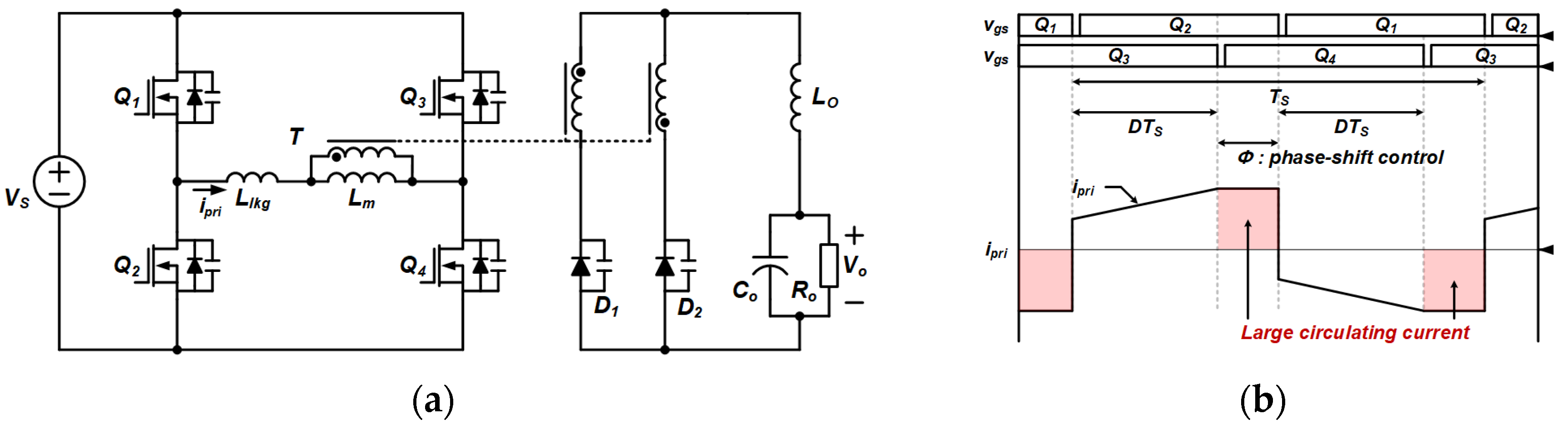
In order to achieve high efficiency and high power density under wide input voltage range and high output current specifications, the conventional LDC converter adopts a phase-shifted full-bridge (PSFB) converter as shown in
Figure 1 due to the zero-voltage switching (ZVS) characteristic and twice powering operation in one switching period of the PSFB converter [
5,
6,
7,
8,
9]. However, since the operating duty ratio at the nominal input voltage is far small, the PSFB converter has large circulating current during freewheeling periods as shown in
Figure 1b, which causes significant high conduction loss at heavy load condition. Furthermore, the PSFB converter has large system volume because of two magnetic components (transformer and output inductor shown in
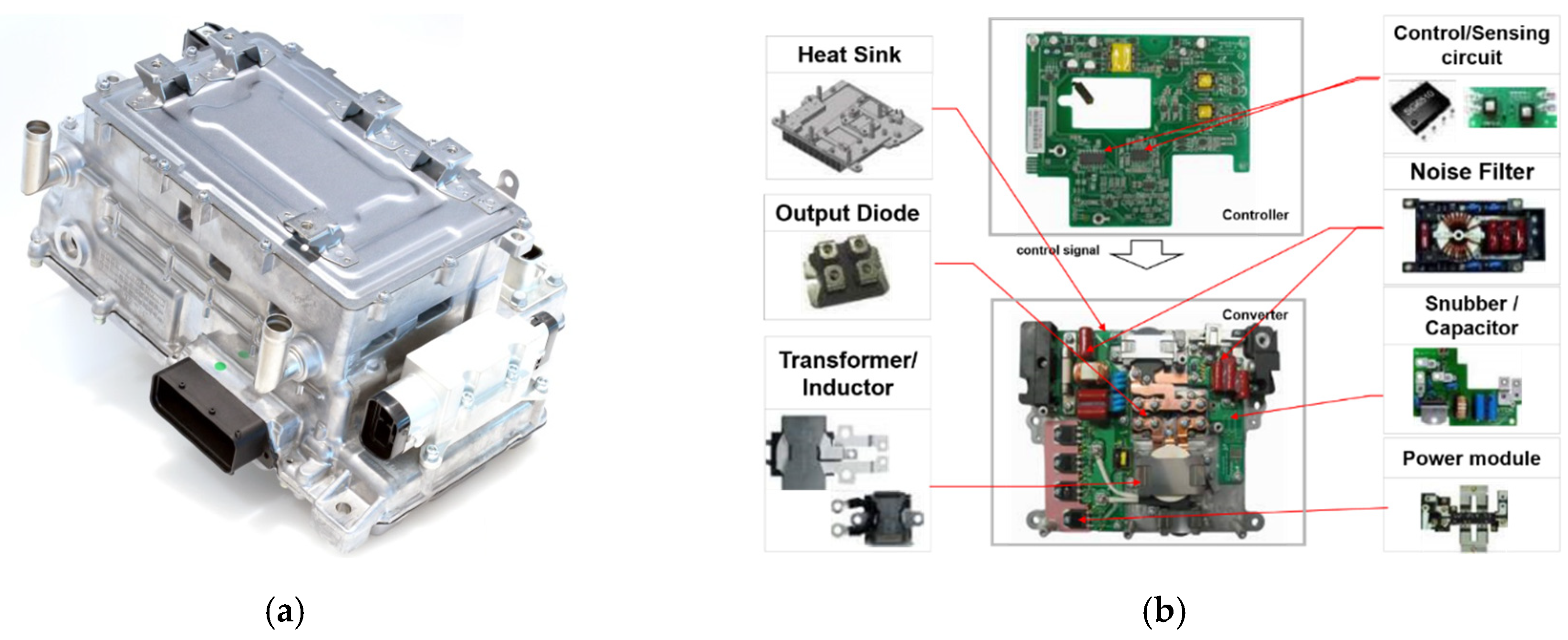
Figure 2b), which must be firmly fixed by using additional bulky devices, and large size of snubber circuits to constraint voltage stresses on the secondary diodes. As a result, the conventional PSFB converter makes difficult to minimize the size of the power control unit (PCU) shown in
Figure 2a which includes an inverter, LDC converter, and control board.
Many DC/DC topologies with low circulating current have been developed to reduce the conduction loss of the conventional PSFB converter [
5,
6,
7,
8,
9,
10,
11]. The converter presented in [
7] reduces the circulating current of the PSFB converter by using large resonant inductance. However, it has serious disadvantages of two additional switches and large volume of auxiliary inductor, which results in increasing the volume and cost of the LDC converter. The converters shown in [
8,
11] can obtain small circulating current by using an additional capacitor in the primary side or a coupled inductor in the secondary side. However, an additional capacitor in [
8] cannot be small to handle high voltage stress and high current stress. A coupled inductor in [
11] requires larger core size compared to a discrete output inductor to keep the same power loss. Moreover, these converters should have two separate magnetic components. Therefore, these converters are still limited in improving power density of the LDC converter.
To complement large circulating current of the conventional PSFB converter, many active-clamp-forward (ACF) converters have been studied [
12,
13,
14,
15,
16,
17,
18,
19]. These ACF converters have advantages of the zero circulating current and low number of switches, which results in lower conduction loss compared to the conventional PSFB converter. However, despite of low conduction loss, these converters suffer from high voltage stress on the primary switches, which becomes far worse taking into account wide input voltage range. As a result, the ACF converters in [
12,
13,
14,
15,
16,
17,
18,
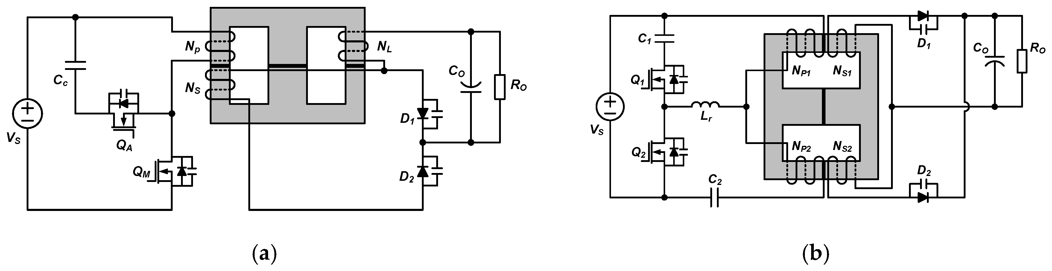
19] should use low performance of Si-MOSFETs increasing conduction loss and switching loss. In order to improve this drawback and achieve high efficiency, the ACF converters can adopt silicon-carbide (SiC) MOSFETs which has high voltage rating, small on-resistance, and small parasitic capacitance. However, using SiC-MOSFETs significantly increases the cost of LDC converter. Moreover, the ACF converters still use two magnetic components increasing the volume of converter. To relieve the voltages stress on the primary switches of the ACF converters, three-switch ACF converters were researched and developed [
14,
15]. However, one of three switches still suffer from high voltage stress. Moreover, the converters in [
14,
15] should use complex driving circuits and two magnetic components. To reduce the number of the magnetic components, ACF converters with an integrated magnetic were represented as shown in
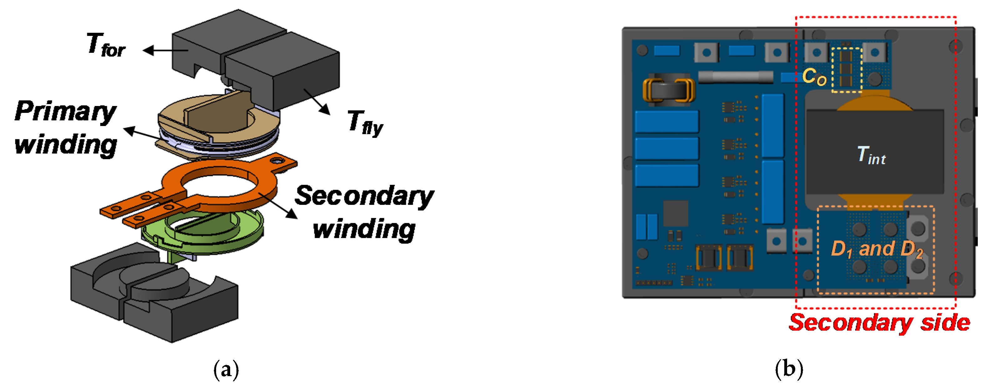
Figure 3 [
16,
17]. Although these converters utilize only one integrated magnetic, the primary and secondary windings are wound the outside of the core shown in
Figure 3, which requires additional shield and structure causing the extra cost and volume to minimize the adverse effect of electromagnetic interference (EMI). As a result, the conventional and previously studied ACF converters have limitations in commercialization especially for vehicle applications.
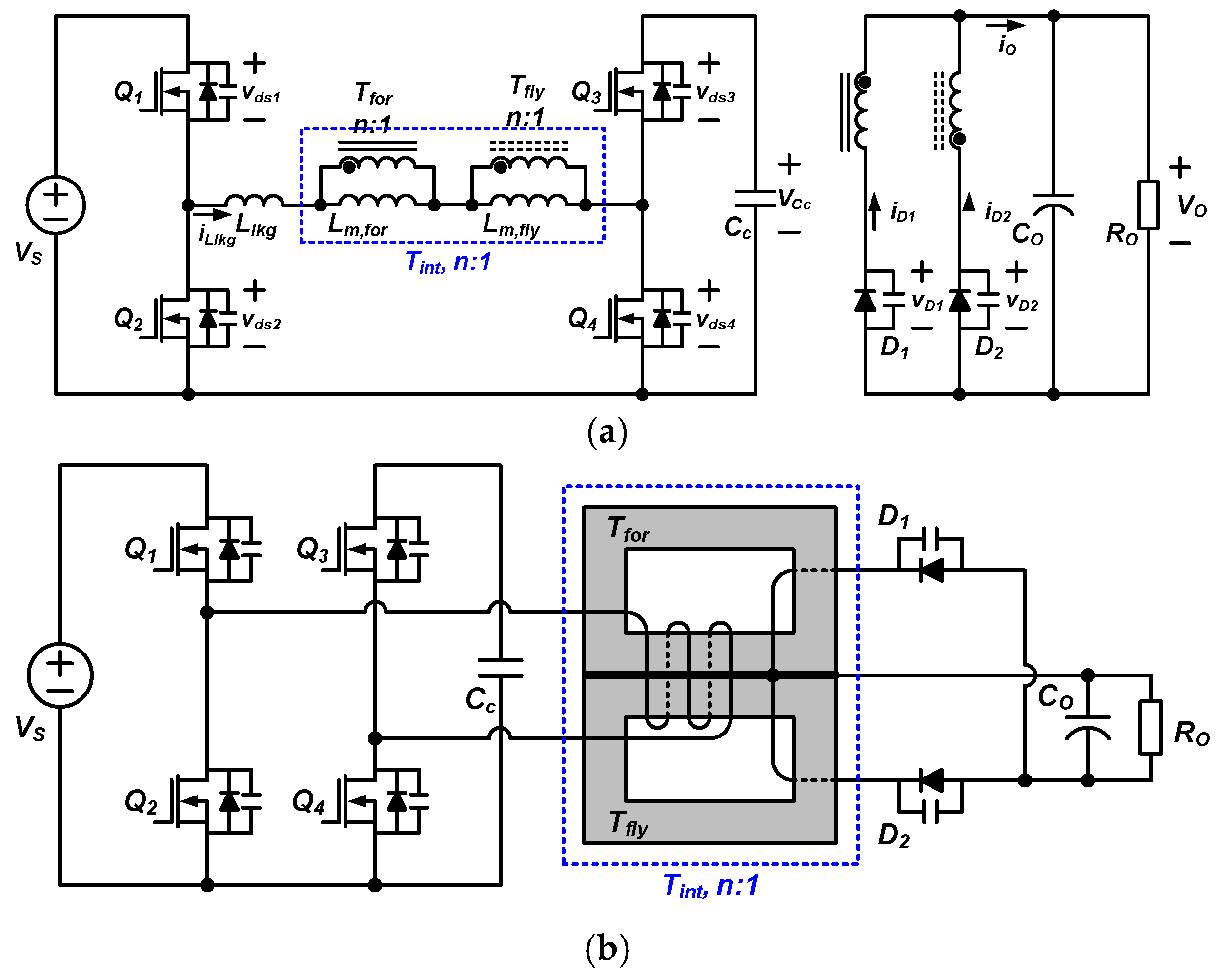
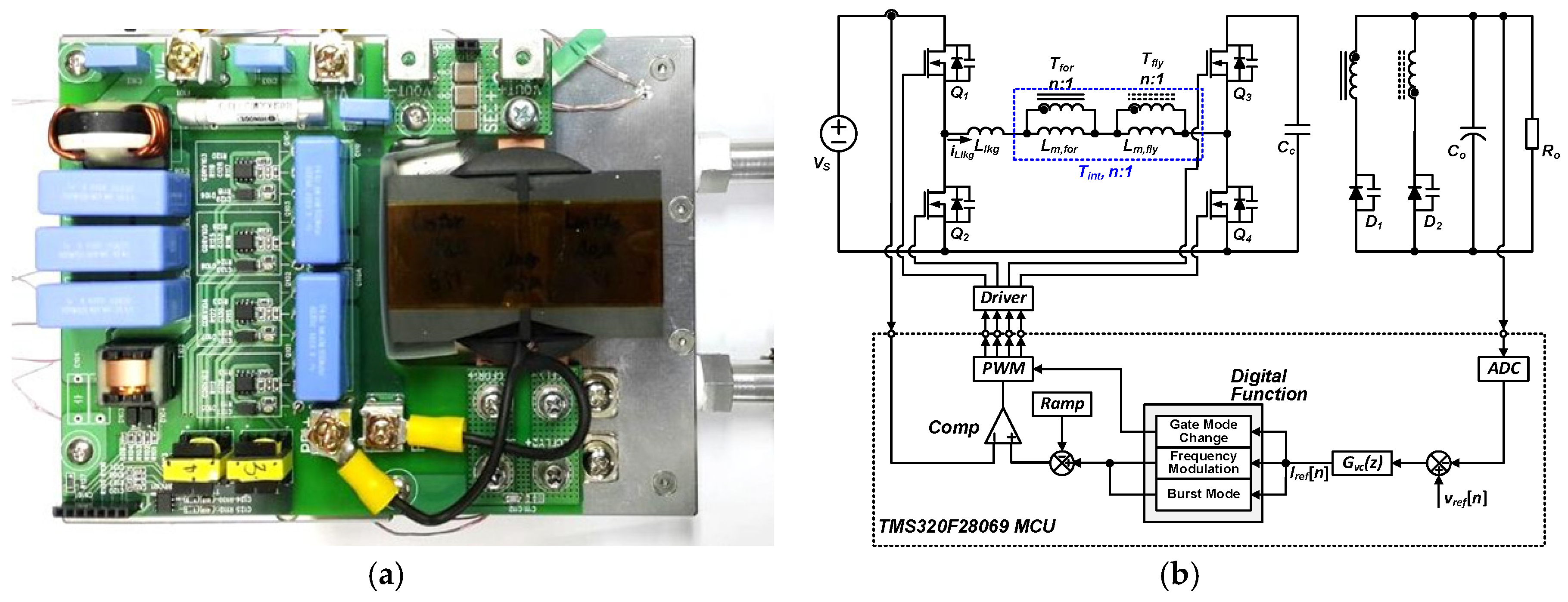
In this paper, the full-bridge active-clamp-forward-flyback (FBACFF) converter adopting an integrated transformer sharing single primary winding is proposed for the LDC converter of vehicle applications. The proposed FACFF converter has the following advantages compared to conventional topologies: (1) active-clamp structure of the proposed converter minimizes the circulating current of the conventional PSFB converter, which results in higher efficiency; (2) full-bridge structure of the proposed converter relieves high voltage stress on the primary switches of the conventional ACF converter and thus the proposed converter can adopt cost-competitive Si-MOSFETs and achieve high efficiency without high-cost SiC-MOSFETs; (3) it can have lower diode voltage stress than the PSFB converter, which enables the proposed converter to use high-current rating diodes; and (4) a proposed single integrated transformer reduces volume and cost of the LDC converter. The primary and secondary windings of the proposed integrated transformer are wound inside of the transformer core, which enables the proposed converter not only to minimize the adverse effect of EMI but also to eliminate additional snubber circuits due to small leakage inductance. As a result, the proposed converter can achieve high efficiency, high power density, and low cost compared to the conventional topologies. In order to verify the validity of the proposed converter, a prototype with 200–310 V input and 1.8 kW (13.6 V/130 A) output was built and the experimental results are presented compared with the conventional PSFB converter which is the most widely used in the commercialized LDC converter.
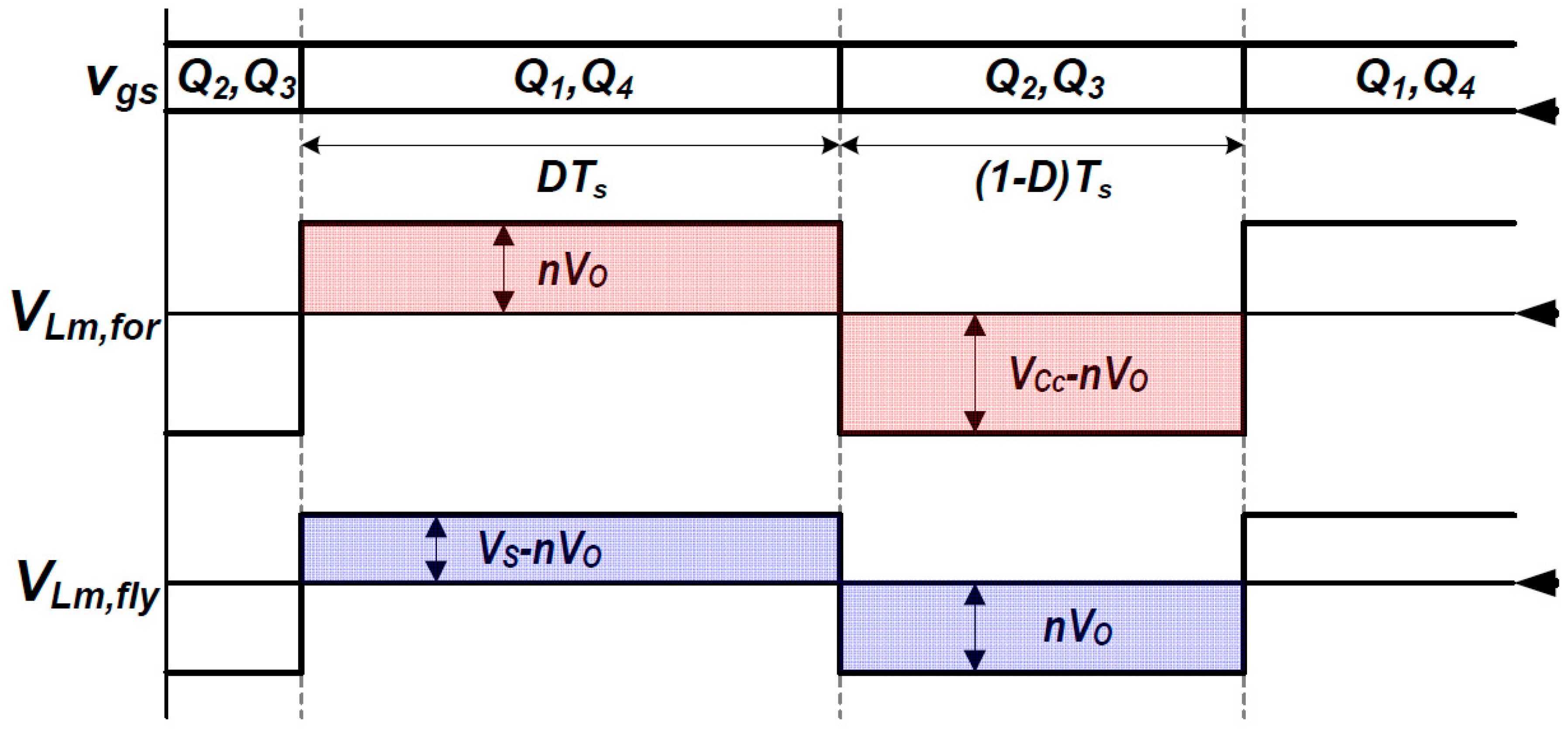
2. Operational Principle
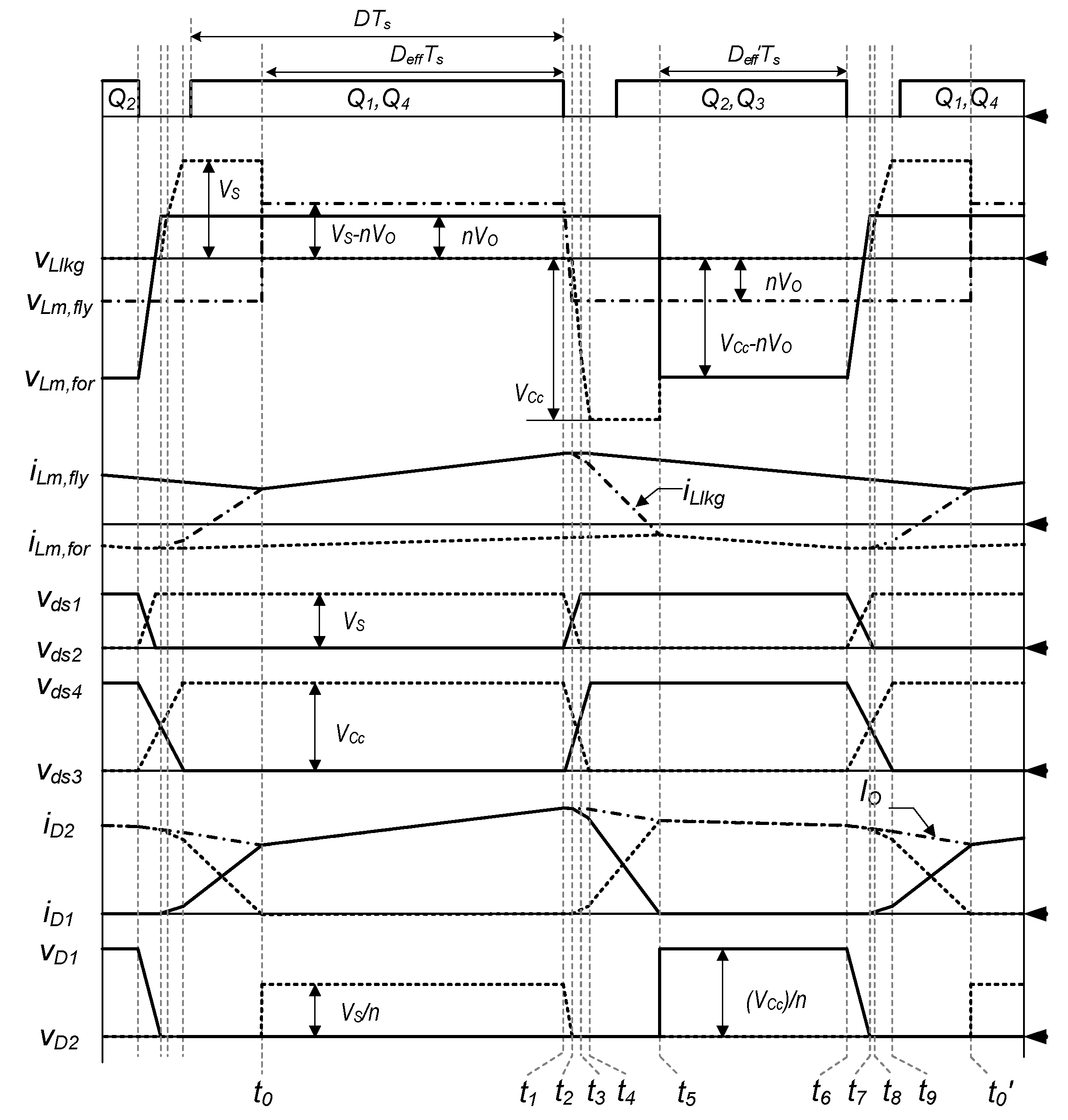
Figure 4 and
Figure 5 show the circuit diagram and operational key waveforms of the proposed converter, respectively. In the proposed converter, the primary switches
Q1 and
Q4 are turned on at the same time to transfer the power from the input to the output through the forward transformer (
Tfor). Meanwhile, the switches
Q2 and
Q3 are driven complementarily with
Q1 and
Q4 to reset
Tfor as well as to deliver the energy stored in the flyback transformer (
Tfly) into the output. For the sake of analysis, several assumptions are made as follows:
- (1)
all parasitic components except for those specified in
Figure 4 are ignored;
- (2)
a clamp capacitor (CC) is large enough to be considered as a constant voltage source (VCc );
- (3)
the output voltage (VO) is constant;
- (4)
the transformer turns ratio (n) of the forward and flyback transformers (Tfor and Tfly) is N/1, where N is the number of the primary winding.
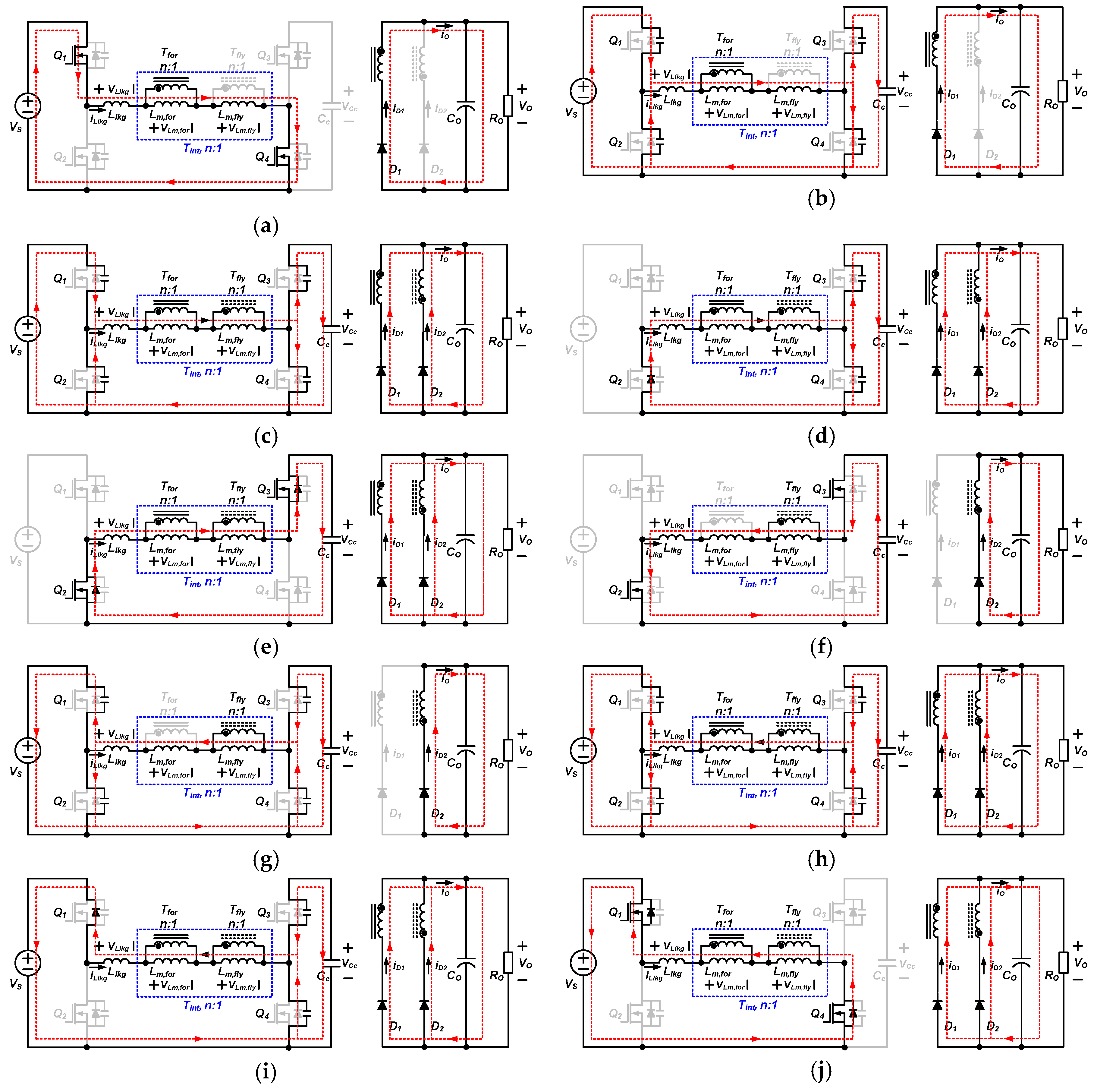
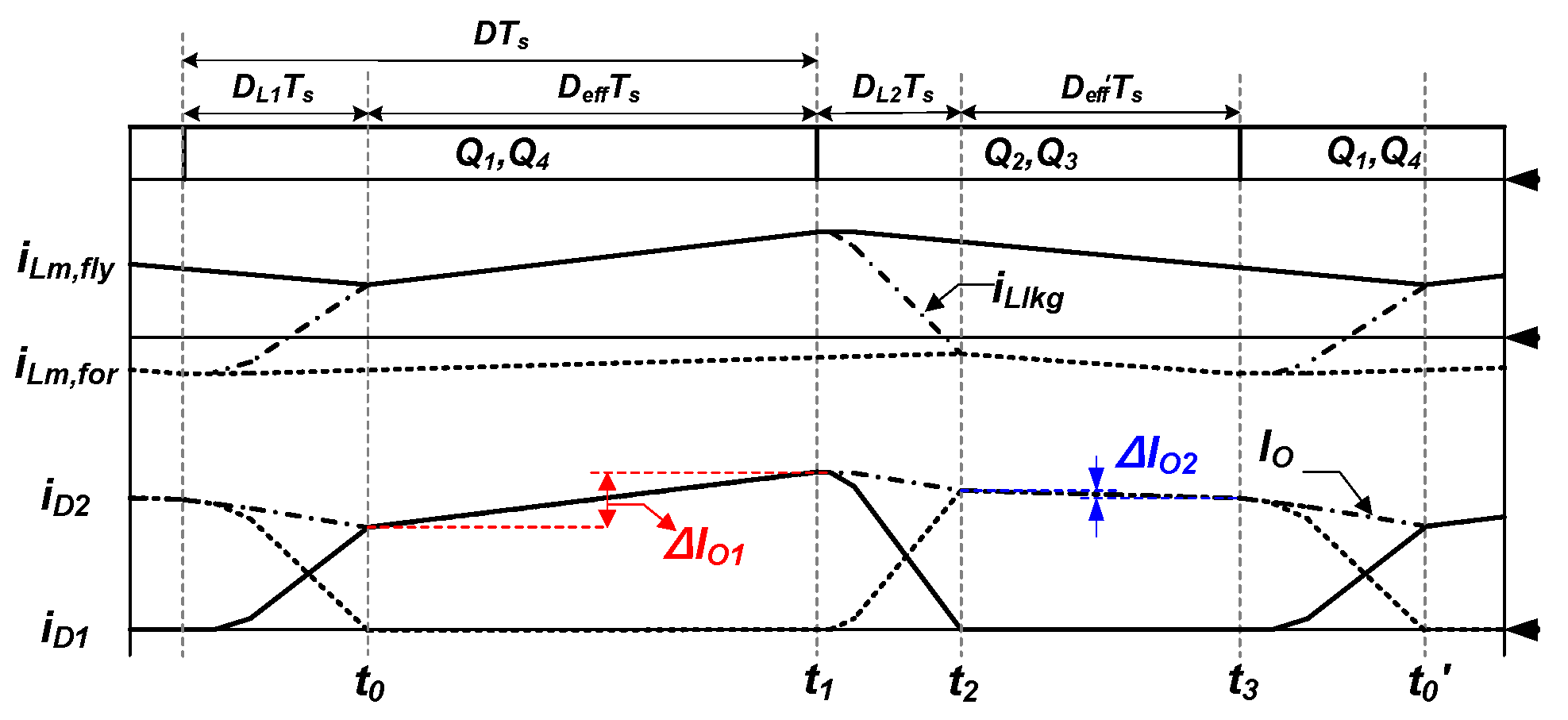
The proposed converter shows 10 operational modes during one switching period and each mode is explained with its topological state as shown in
Figure 6.
Mode 1 [
t0–
t1,
Figure 6a]: At time
t0, after the commutation of the secondary diodes (
D1 and
D2) ends and the leakage inductor current (
iLlkg) reaches to the magnetizing current of
Tfly (
iLm,fly),
nVO, and
VS–
nVO are applied to the magnetizing inductance of
Tfor (
Lm,for) and the magnetizing inductance of
Tfly (
Lm,fly), respectively. As a result,
iLm,for,
iLm,fly, and
iLlkg are linearly increased. The power is transferred to the output through
Q1,
Q4, integrated transformer, and
D1 at this mode. From the voltage across transformers,
iLm,for,
iLm,fly, and current of
D1 (
iD1) are expressed as follows:
Mode 2 [
t1–
t2,
Figure 6b]: After
t1,
Q1 and
Q4 are turned off, and mode 2 begins.
iLm,fly is the same as the reflected load current (
IO/n) charges
Coss1 and
Coss4 and discharges
Coss2 and
Coss3. Thus, the voltages across
Q1 and
Q4 (
vds1 and
vds4) simultaneously increase to
VS/2, and the voltages across
Q2 and
Q3 (
vds2 and
vds3) decrease to
VS/2 and
VCc–
VS/2, respectively. Thus, the voltage across
Lm,fly (
vLm,fly) is decreased from
VS–nVO to –
nVO so that the sum of the voltages across
Lm,fly and
Lm,for is zero at the end of this mode.
Mode 3 [
t2–
t3,
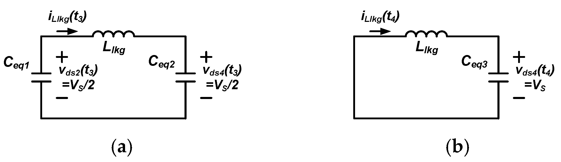
Figure 6c]:
vLm,fly reaches –
nVO at
t2,
D1, and
D2 start to conduct. The leakage inductance of the integrated transformer (
Llkg) resonates with parasitic output capacitors (
Coss1,
Coss2, Coss3, and
Coss4). The equivalent circuit of this mode is illustrated in
Figure 7a. From this Figure, the energy stored in
Llkg charges
Coss1 and
Coss4 and discharges
Coss2 and
Coss3. Thus,
vds1 and
vds4 are increased, and
vds1 is clamped to
VS. Meanwhile,
vds2 and
vds3 are decreased to zero and
VCc–
VS, respectively.
Mode 4 [
t3–
t4,
Figure 6d]: After
vds2 reaches to zero at
t3, mode 4 starts. In this mode, only
Coss3 and
Coss4 are continuously discharged and charged by the resonance with
Llkg, respectively.
vds3 decreases to zero and
vds4 increases to
VCc. The equivalent circuit of this mode is depicted in
Figure 7b. Based on Mode 3 and Mode 4, the ZVS condition of
Q2 and
Q3 are:
where
Coss =
Coss1 =
Coss2 =
Coss3 =
Coss4.
Mode 5 [
t4–
t5,
Figure 6e]: At time
t4,
vds2 and
vds3 are 0 V, and
iLkkg flows through body diodes of
Q2 and
Q3. As a result,
Q2 and
Q3 can achieve the ZVS operation. Moreover, since the sum of
vLm.for and
vLm.fly is zero, –
VCc is applied to
Llkg. Thus,
iLlkg is linearly decreased to
iLm.for with the commutation between
D1 and
D2.
iLlkg at this mode is:
From (5), the commutation period, where the input power is not transferred to the output, can be approximated as LlkgIO/(nVCc).
Mode 6 [
t5–
t6,
Figure 6f]: After the commutation of
D1 and
D2 ends, the voltage on
D1 reaches
VCc/n and the reset operation of
Tfor starts by
vLm,for (=
nVO–
VCc). Meanwhile, the energy stored in
Tfly is delivered to the output because
vLm,fly is –
nVO. As a result,
iLm,for,
iLm,fly, and current of
D2 (
iD2) are expressed as follows:
Mode 7 [
t6–
t7,
Figure 6g]: After
t6,
Q2 and
Q3 are turned off, and mode 7 starts.
iLm,for charges
Coss2 and
Coss3 and discharges
Coss1 and
Coss4. Thus,
vds2 and
vds3 are increased to
VCc/2.
vLm,for is increased from
VCc–
nVO to
nVO. On the other hand,
vds1 and
vds4 are decreased to
VS–VCc/2 and
VCc/2, respectively. This mode ends when
vLm,for reaches to
nVO and the sum of the voltage on the magnetizing inductances is zero.
Mode 8 [
t7–
t8,
Figure 6h]:
vLm,for reaches
nVO at
t7 and
D1 and
D2 conduct. Thus,
Llkg resonates with
Coss1,
Coss2, Coss3, and
Coss4. The equivalent circuit of this mode is illustrated as in
Figure 7. From this Figure, the energy stored in
Llkg charges
Coss2 and
Coss3 and discharges
Coss1 and
Coss4. Thus,
vds2 and
vds3 are increased and
vds2 is clamped to
VS, whereas
vds1 and
vds4 are decreased to zero and
VCc–
VS, respectively.
Mode 9 [
t8–
t9,
Figure 6i]: After
vds1 reaches to zero at
t8, Mode 9 begins. In this mode, only
Coss3 and
Coss4 are continuously charged and discharged in accordance with the resonance with
Llkg. As a result,
vds4 is decreased to zero and
vds3 is increased to
VCc. The equivalent circuit of this mode is depicted in
Figure 7d. Based on Mode 8 and Mode 9, the ZVS condition of
Q1 and
Q4 is:
Mode 10 [
t9–
t0’,
Figure 6j]: After
vds1 and
vds4 become 0 V,
iLlkg flows through body diodes of
Q1 and
Q4. Thus,
Q1 and
Q4 can achieve the ZVS condition. Moreover, similar to Mode 5, since the sum of
vLm.for and
vLm.fly is zero,
VS is applied to the
Llkg. Thus,
iLlkg is linearly increased to
iLm.flly with the commutation between
D1 and
D2.
iLlkg at this mode is:
From (10), the commutation period can be derived as LlkgIO/(nVS).
4. Experimental Results
To prove the validity of the proposed converter, a 1.8 kW prototype shown in
Figure 11a was built with the specification of
VS = 200–310 V,
VO = 13.6 V,
fS = 125 kHz at 200 V input – 150 kHz at 310 V input. We also implemented a conventional PSFB converter.
Table 3 summarizes the details of two prototypes. In this chapter, the commercialized PSFB converter was designed for IONIQ HEV (made by HYUHNDAI motor company) and is used as the conventional converter to compare the performance of the proposed converter.
To regulate the output voltage, as shown in
Figure 11b, the proposed converter used a DSP that is TMS320F28069PZT with 90 MHz clock frequency and 12-bit analog to digital conversion module. The DSP is used to implement the output voltage control and the switching frequency variation. The duty to output voltage transfer function of the proposed converter can be derived like a buck converter as follows:
where γ is 1 +
Lm,fly/
Lm,for.
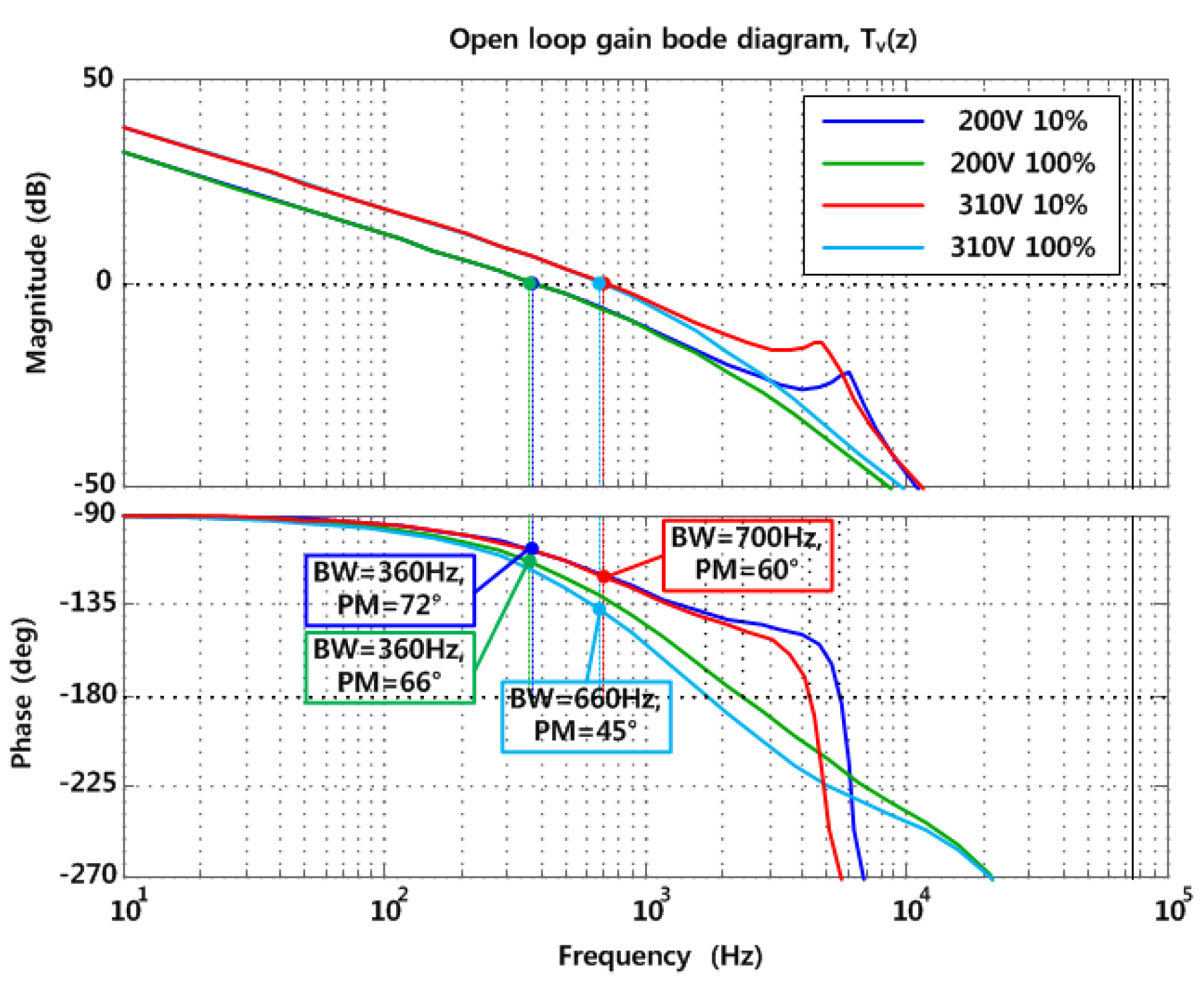
The loop gain (
Tv(
z)) of the proposed converter adopting the voltage compensator is illustrated in
Figure 12. The voltage compensator (
Gvc(
z)) was designed for minimum 360 Hz bandwidth and 45° phase margin for the prototype of this paper.
In addition, since the DSP is placed in the secondary side, the pulse transformer which can transfer gate signals from the secondary side to the primary side is implemented. In addition, for measuring the performance of the conventional and proposed converters, NFES2000S is used as an input power supply, Chroma DC Electronic load 63203 as an output electronic load, YOKOGAWA WT1600 as an input power analyzer, FLUKE 45A digital multi-meter for the output voltage and current measuring, and Wave-runner 64xi TELEDYNE LECROY to capture the experimental waveforms.
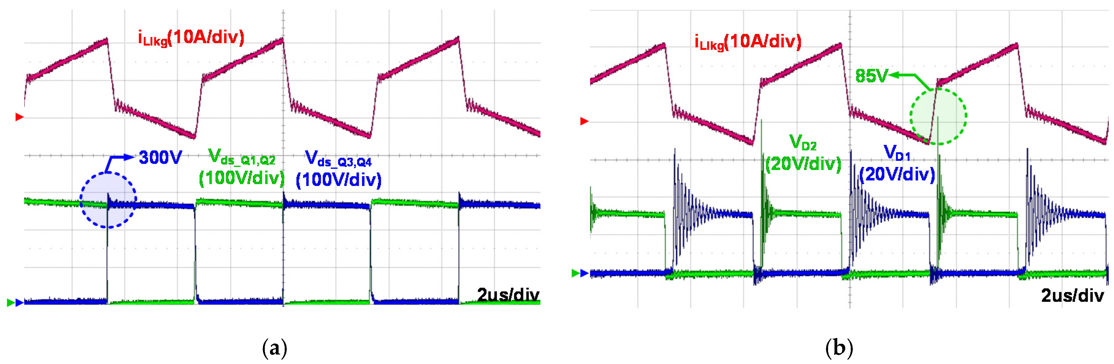
Figure 13 shows the experimental waveforms of the proposed converter at the nominal input voltage (
VS = 270 V) and full-load condition with the 150 kHz switching frequency. As shown in
Figure 13a, due to the ACF structure, there is no circulating current and only small commutation current occurs during the switch transition. Moreover, voltage stresses on the primary switches of the proposed converter is far lower than 650 V which is general breakdown voltage of high-performance Si-MOSFETs. As a result, the primary conduction loss of the proposed converter can be considerably reduced compared to the conventional PSFB converter. Moreover, the propose converter cuts the production cost by utilizing Si-MOSFETs and the integrated transformer with single and inside wounded primary and secondary windings.
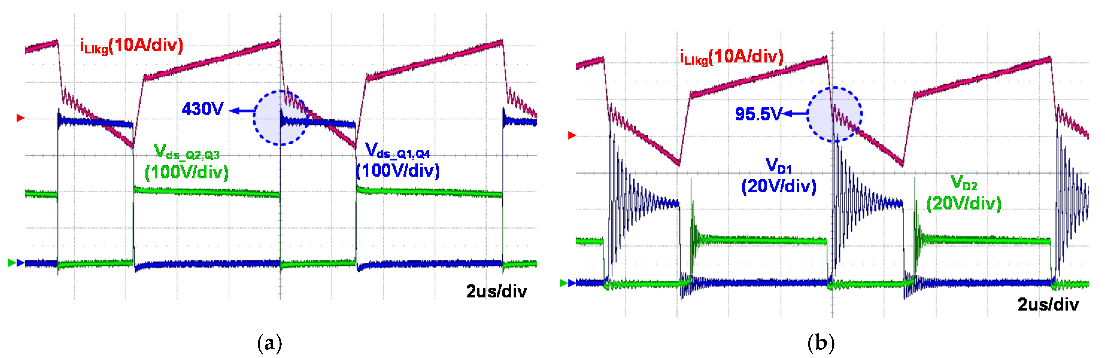
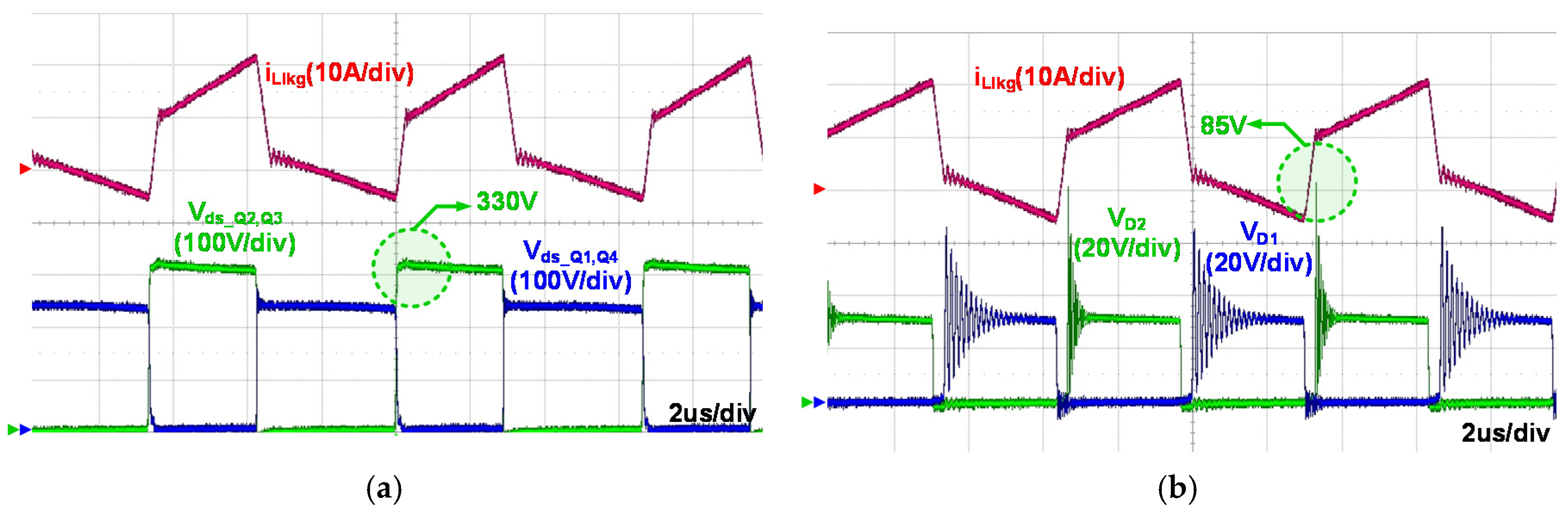
Figure 14 and
Figure 15 present the key experimental waveforms at the minimum and maximum input voltage conditions under the full load condition. As shown in
Figure 14, in the minimum input voltage condition (
VS = 200 V), since the maximum switch voltage stresses are determined by the actual duty ratio that is sum of the effective duty ratio and the duty loss during the commutation period, the switching frequency varies from 150 kHz to 125 kHz at the minimum input voltage condition to reduce the ratio of the commutation period in the total switching period. As a result, the voltage stresses on the primary switches are well restricted near 400 V, and the secondary diode voltage stresses are under 100 V. Since the duty ratio (
D) of the proposed converter can be designed to be over 0.5, the proposed converter well regulates the output voltage at the minimum input voltage condition with
D = 0.605. Moreover, as can be seen in
Figure 15, the voltage stresses on the switches and diodes are under 400 V and 100 V in the maximum input voltage condition (
VS = 310 V). Although the voltage stresses on the switches and diodes varies according to the input voltage conditions, all of them are well controlled and restricted to be suitable for high performance Si-MOSFET with low cost and low on-resistance. Furthermore, the ZVS operation of the proposed converter is achieved even in the worst-case condition such as the high input voltage and full-load conditions shown in
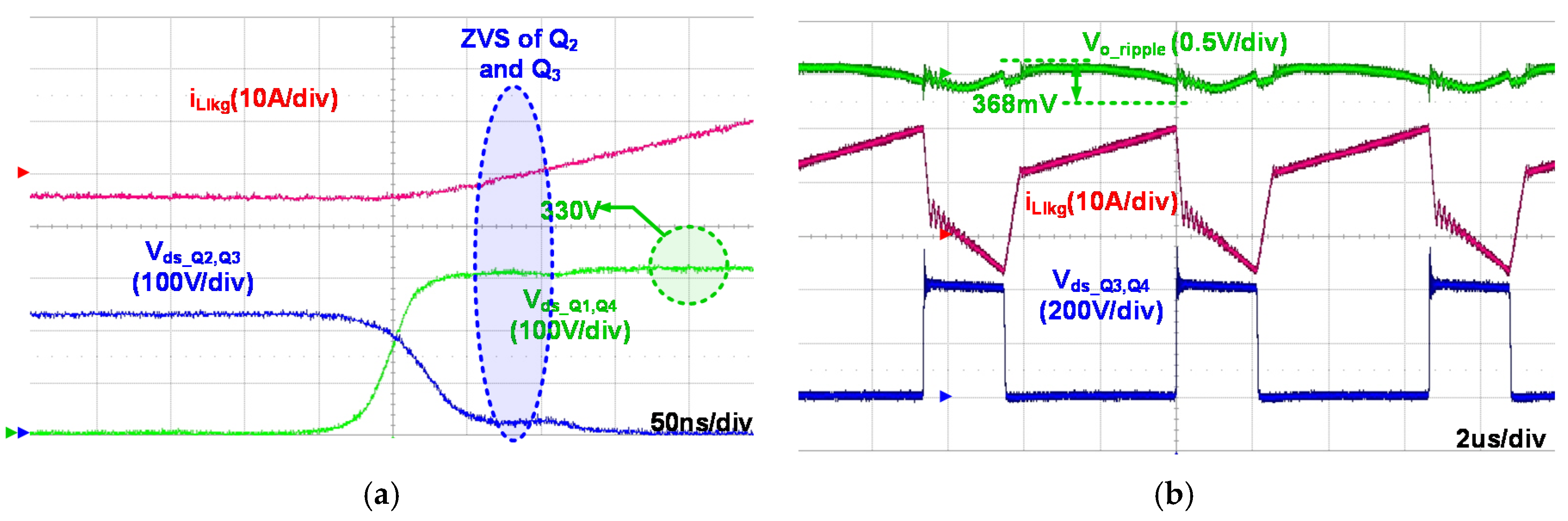
Figure 16a.
Figure 16b shows the output voltage ripple of the proposed converter. The maximum output voltage ripple is under 500 mV regardless of the input voltage and load conditions (500 mV is the output voltage ripple requirement of LDC converter for vehicle applications). This verifies that the magnetizing inductances of the proposed integrated transformer is adequately designed and chosen. Thus, despite the integrated transformer, the proposed converter can effectively constrain the output current ripple.
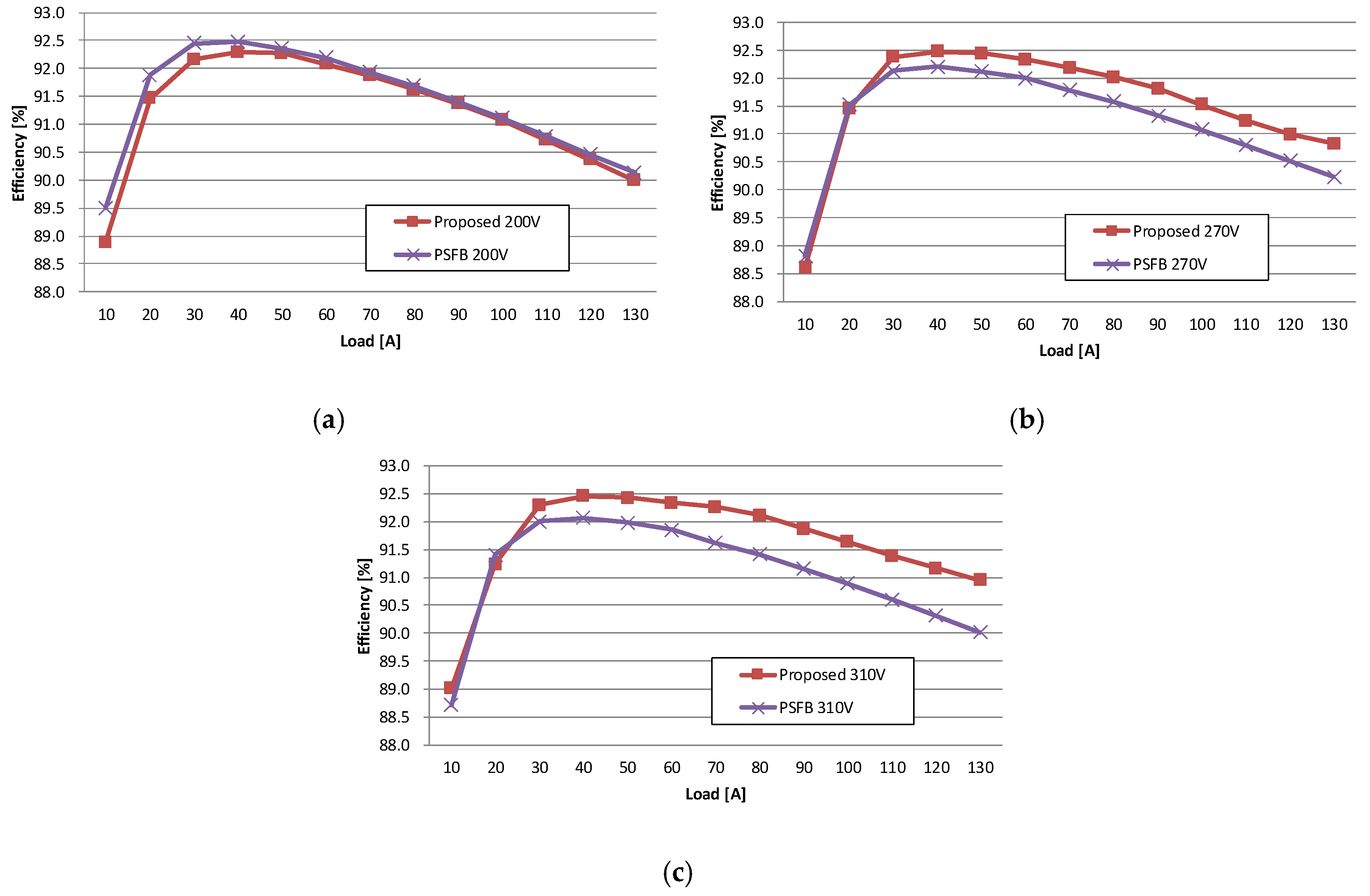
Figure 17 shows the measured efficiency of the proposed and conventional PSFB converters. In the minimum input voltage condition, the efficiency of the proposed converter is almost the same as that of PSFB converter because the PSFB converter operates with a duty ratio near 0.5. Meanwhile, in the nominal and maximum input voltage conditions, as previously analyzed, the proposed converter shows higher efficiency over the 30% load conditions due to the reduced circulating and conduction loss of the
Q2 and
Q3 switches. On the other hand, because of large core loss and small magnetizing inductances of the integrated transformer, the efficiency of the proposed converter is similar to that of the conventional PSFB converter under light load condition. However, since the importance of the high heavy load efficiency is gradually increased, the proposed converter is attractive for the LDC converter of the vehicle applications. Moreover, the proposed converter is a very promising converter for other wide input and high output power applications due to its high efficiency and high power density characteristics.


