1. Introduction
With the increasing popularity of the smart grid, the applications of the intelligent electronic equipment have become more essential. Intelligent electronic devices such as electronic transformers, intelligent components, and condition monitoring in smart substations have begun to be widely used [
1,
2,
3]. Furthermore, the advantages of intelligent electrical equipment have been verified theoretically. However, high- or low-voltage equipment co-existing in smart substations has led to the complexity of these substations’ electromagnetic compatibility (EMC) [
4]. The reliability of intelligent electronic equipment that is arranged next to high-voltage (HV) gas insulated switchgear (GIS) is greatly reduced [
5], which has become one of the restrictions for the intelligent substations’ development and application [
6].
Various kinds of electromagnetic (EM) disturbance will be encountered during the substation circuit breaker (CB) operation. With the increase of the transmission voltage level, the accompanying electromagnetic interference (EMI) problems will be more serious [
7]. Based on electronic technology, intelligent equipment is sensitive to the EMI. In the limited space of substations, how to ensure the reliability of intelligent electronic equipment in complex EM environments has become the focus of research in the power industry [
8].
Current or voltage transformers are important for power measurement, control, and protection in power systems. Their accuracy and reliability are closely related to the safety, stability, and economic operation of the power systems. With the development of the Chinese electric power industry, the transmission capacity of the power system is constantly increasing, and the operating voltage level of the power grid is getting higher [
9]. Traditional transformers are easy to saturate, and the output is affected by the secondary side load and other shortcomings. Compared with the traditional transformers, electronic transformers have many advantages such as small size, light weight, wide frequency band, no saturation phenomenon, reliable insulation and so on. Therefore, electronic transformers are more compliant with the smart grid. However, in terms of reliability analysis, further research work is still required [
10].
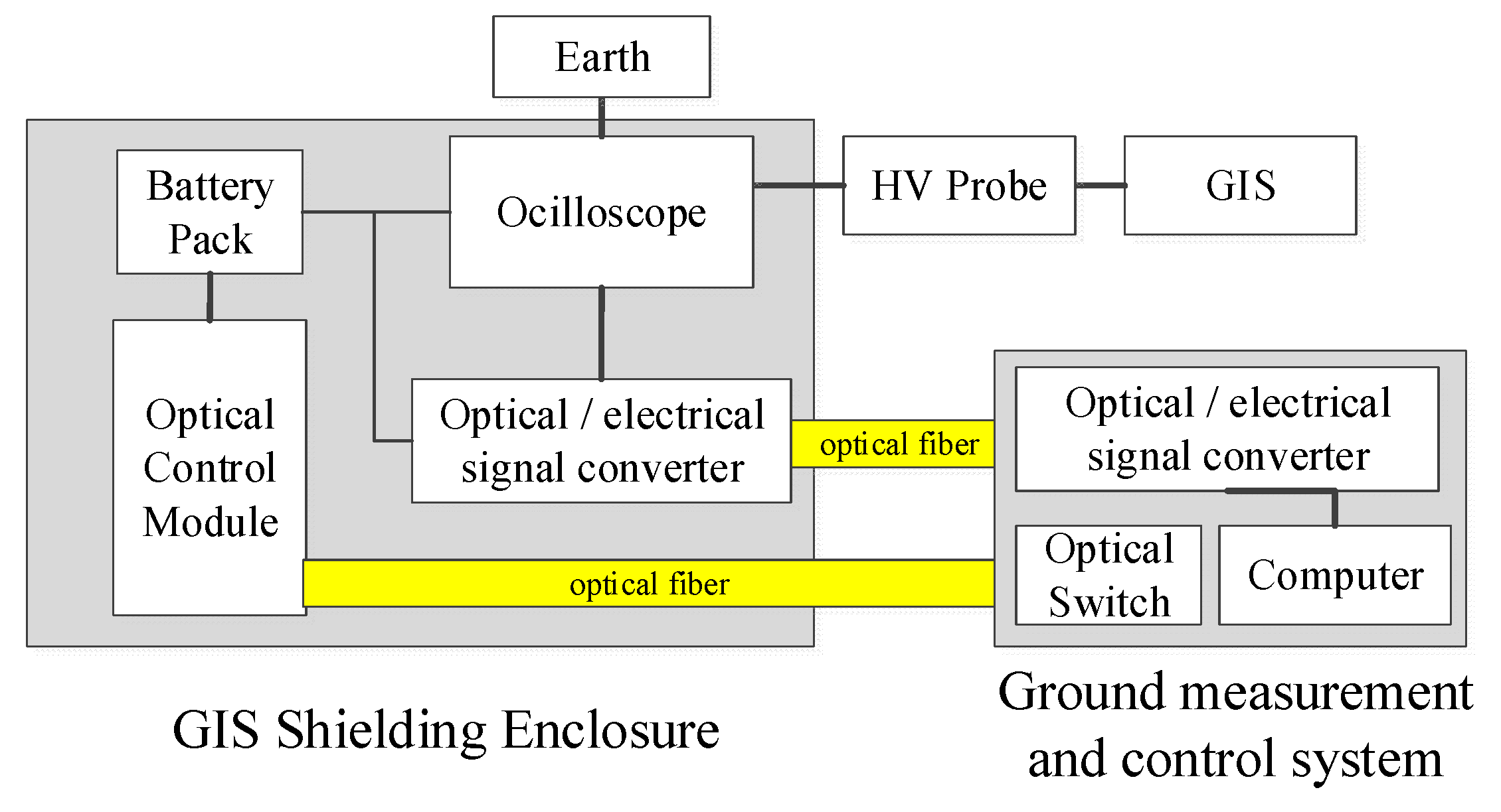
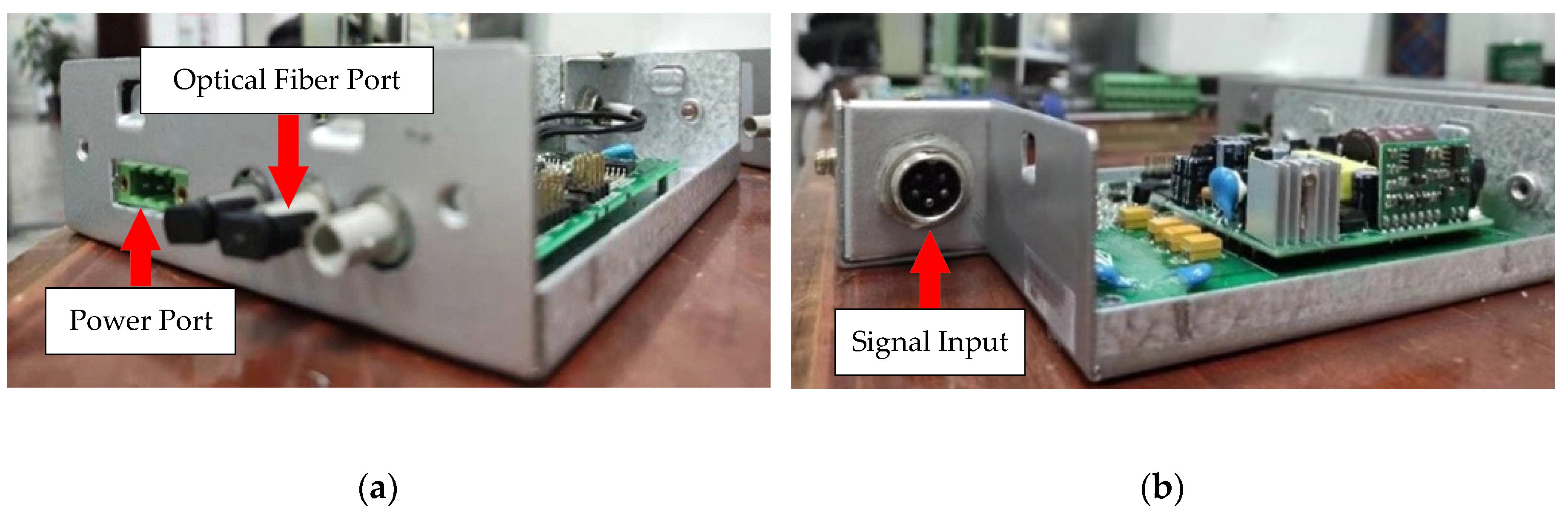
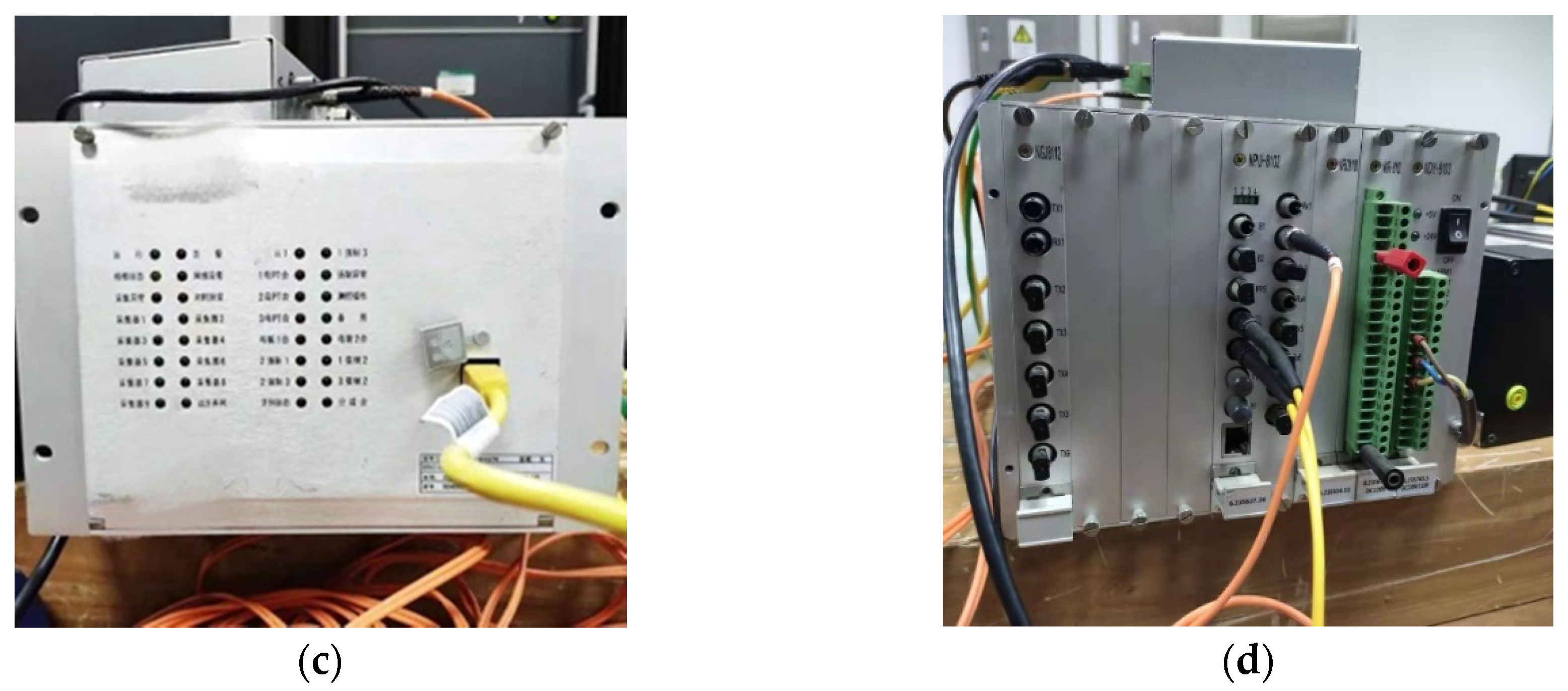
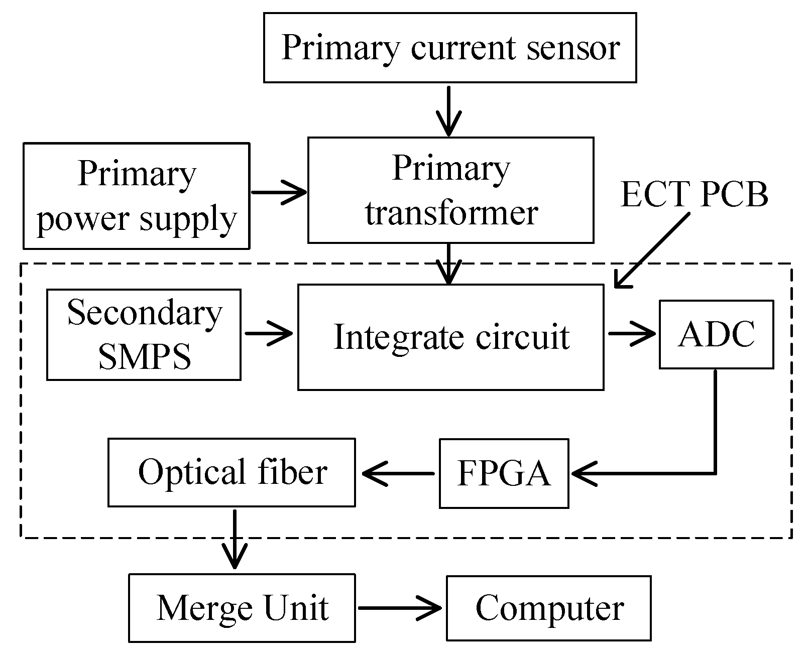
Figure 1 shows the monitoring system of the electronic transformer acquisition card.
At present, almost all of the intelligent substations with voltage levels above 110 kV have applied electronic transformers [
11]. On the one hand, digital acquisition circuits and communication network systems have been added to electronic transformers, which have brought about many technical advantages. On the other hand, close installation next to the HV side will also cause some new problems that are not had by traditional transformers [
12]. Actually, the practical application results show that the stability and reliability of electronic transformers need to be further improved.
Concerning the immunity testing, some scholars have already researched the test on EMC [
13,
14,
15,
16]. Trenkler and McBride developed the test methods to characterize the shield performance when the equipment under test (EUT) was applied to metal sheets [
17]. Finney discussed some special systems, such as telephone exchanges, that are too large and complex to implement the EMC test in the typical way [
18]. In [
19], Tas and Pythoud developed a novel device to assess the immunity test capabilities of laboratories. In [
20], Medico described a novel machine learning based approach for error detection, which only requires the raw output data from a susceptibility test.
For the modeling, a mathematical model of electrostatic discharge (ESD) was created by Liu using the transmission line theory to study the immunity of electronic system [
21]. In [
10], through extracting the intrinsic behavioral characteristics of printed circuit board (PCB), and the transmission line (TL) model of the cable, a new analytical model of system-level for EM immunity design was established by Gao and his team. For the immunity of integrated circuits (IC), Ayed studied an analog-to-digital converter (ADC) via probe injecting resistive radio frequency (RF). With passive distribution network (PDN) representing the same parts of the circuit, the immunity behavior (IB) blocks the model circuits’ response to the EMI. This model improved the prediction of ICs immunity [
22].
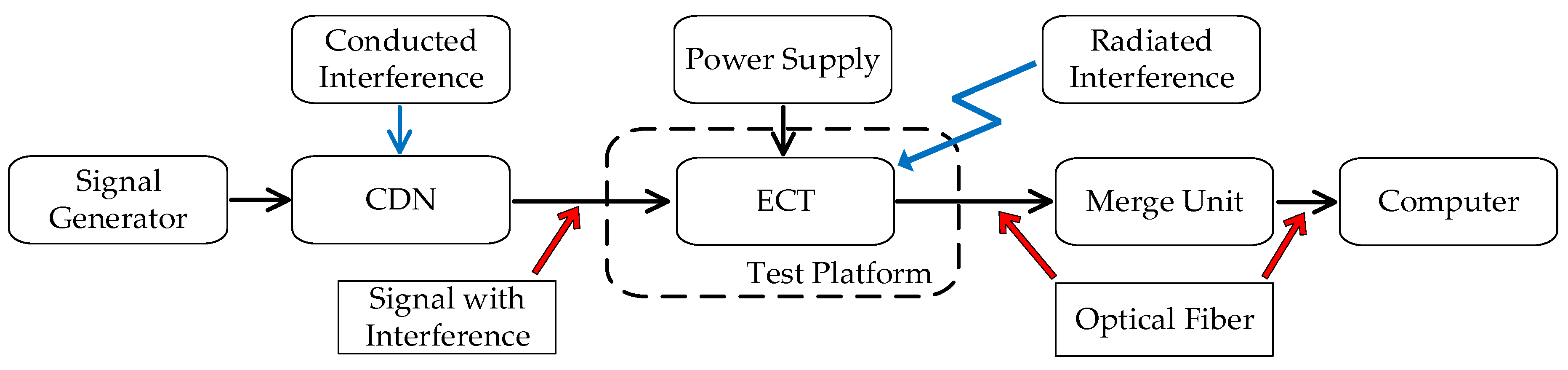
In order to study the working reliability of the electronic transformer, this paper takes an electronic current transformer (ECT) acquisition card as an example, and measures the true EM environment in a smart substation. Then, under lab conditions the authors measured, analyzed, and evaluated the EM immunity of the ECT’s signal integrity under international electrotechnical commission (IEC) standard. In this paper, therefore, the authors present a new method by using principal components analysis (PCA) to evaluate the ECT’s degree of output waveform distortion.
This paper is organized as follows. In
Section 2, the test condition based on IEC is introduced and the substation’s EM environment is measured. In
Section 3, the PCA method is presented, and the detailed disturbed distortion (
DD) is presented. In
Section 4, the area of distortion (AD) of the ECT’s output waveform under different standard settings is calculated and discussed. Conclusions are drawn in
Section 5.
3. Method to Quantifying the Disturbance of ECT Acquisition Card Output Waveform
As discussed above, the envelope can simplify the output waveform and reflect the output characteristics when the ECT acquisition card is disturbed. The upper envelope is therefore used to indicate the degree of disturbance in this paper. However, an envelope waveform is good for use in qualitative analysis. Despite that, this method cannot directly and quantitatively show how serious the acquisition card is disturbed. Typically, we use mean or variance value to show the true condition of the ECT output. For the large amount of data, these methods are not intuitive to show the output results. If the large volume of output data is directly processed, it will also face the problem of phase correction. Therefore, this paper proposes a new data dimension-reduction method to optimize and simplify the data model. The proposed method can quantify the degree of how the ECT acquisition card is disturbed by EMI.
Principal components analysis (PCA) is a dimension-reduction method. The purpose of this model is to find the main components in the data, that is, the dimensions with the highest data variation. We reduced the dimension of the dataset by converting a large number of variables to a smaller number that still contained most of the information in the collection. Reducing the number of variables in a dataset naturally comes at the expense of accuracy. But dimension is reduced to keep the data as simple and accurate as possible. Smaller data sets are easier to explore or visualize, and make it easier or faster for computers to analyze data without having to deal with irrelevant variables.
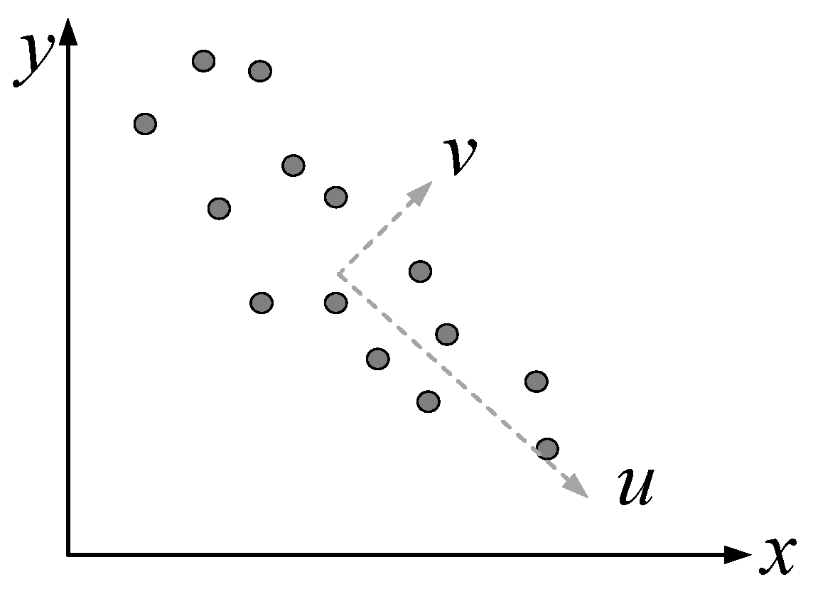
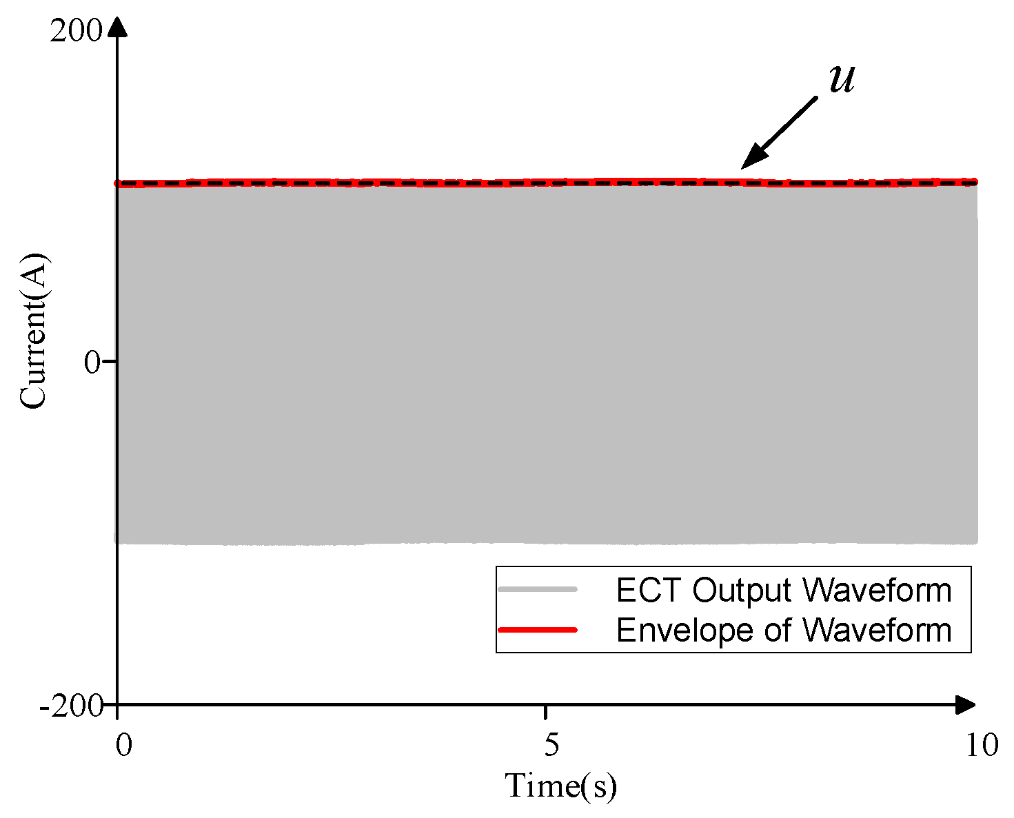
To visualize the model,
Figure 9 shows an example of data in two dimensions.
There are a series of irregular scattered points distributed in a two-dimensional coordinate system. At this point, we need to compress this part of the data into one dimension. The process of reducing the two-dimensional data to one dimension is the projection of points onto a line. Those points after projection are the reduced data. According to the principle of PCA, the larger the variance after the projection of the data, the better. Thus, the dimension-reduction results in the graph can be obtained. The longer line u in the graph represents the data projection after dimension-reduction. Since the data in the direction of u varies the most, the data in this direction is often referred to as the first-principal component. Similarly, we can define the second-principal component v, which are the data with the second largest change. The data changing direction of the second-principal component v are perpendicular to the data changing direction of the first principal component u.
The following is a discussion on how to obtain the dimension-reduction results from mathematics. It is assumed that there are
n data for dimension-reduction, and the data have
m dimensions. The
i-th data is denoted as:
For a simple derivation, suppose the center of these
n data is the origin, and we have
where
l equals from 1 to
m.
Assuming the unit vector of the dimension-reduction line by
Then the projection of the
i-th point on this line is shown in the formula
where the
XiUT is the length of the projection.
According to the principle of PCA, we hope that after dimension-reduction the variance of the data is larger. Note that the center of the data is inconvenient in the process of dimension–reduction, and it is still the origin point. So, the variance of the data after dimension-reduction is shown in the formula
Note that
XiUT is a real number, so we have
According to Equation (6), we make further transformations to get the formula
If we take Equation (8) as
C, then it is an
m ×
m matrix. Actually,
C is the covariance matrix of the data, so the dimension-reduction principle of PCA is
Thus, the optimal dimension-reduction vector, namely the estimation formula of the first principal component, is obtained
For the optimization problem shown in Equation (10), it can be proved mathematically, when U is the eigenvector of matrix C and the corresponding eigenvalue reaches the maximum value, the maximum value of UCUT is reached. In other words, to reduce the data to one dimension is to find the maximum eigenvector of the matrix C. After obtaining this vector, the reduced dimensional data can be obtained according to the formula (i.e., the original sample points are projected onto the corresponding coordinate of the eigenvector respectively). Similarly, it can be proved that to reduce the data to k dimension, the first k eigenvectors of matrix C are required.
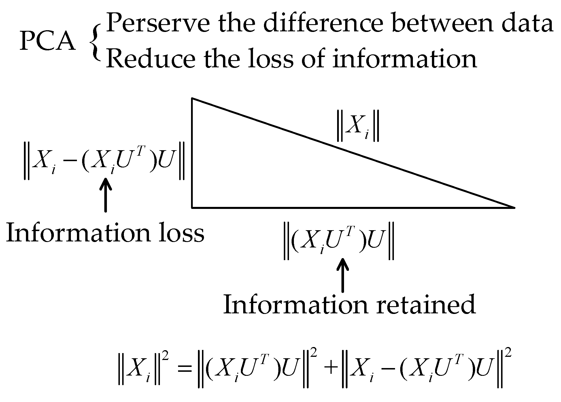
It can be seen from the above that the design of PCA is to make the dimensionless data retain as much information as possible. In fact, dimension-reduction can be considered from another perspective: how to minimize the loss of information in the process of dimension-reduction. Following the above example of reducing the data to one dimension, for the
i-th point, the reduced data is
So, the lost information is
The distance from the original data to the dimensionless line is the lost information. To minimize the amount of information lost, the distance from the original data to the dimensionless line needs to be minimized. According to the principle of minimum loss of information, the estimation formula of the optimal dimension reduction vector is as follows
As shown in
Figure 10, it can be proved mathematically that the two optimization problems of the formula are equivalent. Therefore, the principal components analysis achieves two goals in the process of dimensionality reduction, one of which is to preserve the difference between data as much as possible, and the other is to reduce the loss of information as much as possible.
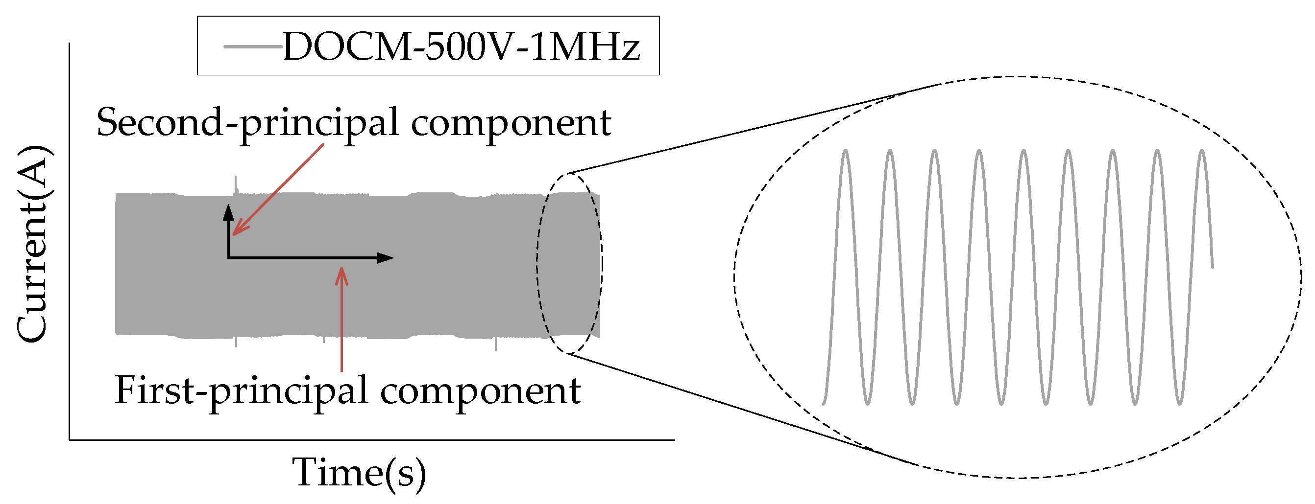
Next, PCA is used to process the output data of the ECT acquisition card. It can be seen in
Figure 11 that the data can be classified as two directions. The output waveform distortion after being disturbed will have randomness and the output data is very large, which will affect the offset of the first principal component vector coordinates.
We select a set of output waveform data of the ECT under normal working conditions. After implementing the envelope process, we have the raw data to perform PCA. According to the steps of PCA, we first calculated the expectations of the raw data. The average value of the upper envelope
y and the time
x was 104.1251 and 4.9999 respectively. Subtracting the
x and
y values from the sample data, and then calculating the total covariance gave us
The diagonal line is the variance of x and y, and off-diagonal is the covariance.
If the covariance is greater than zero, it means that x and y are positively correlated, and if the covariance is less than zero, it means that x and y are negatively correlated. The greater the absolute value of the covariance, the greater the influence of the two on each other; otherwise, the smaller the influence of the two on each other. When the covariance is zero, the two groups of data are relatively independent.
The eigenvalues and eigenvectors for solving the covariance are:
It can be seen that the larger eigenvalue is 20.9535, and the corresponding eigenvector is (−0.9998, 0.02151)
T. Next, we projected the sample points onto the selected eigenvectors. The sample matrix of data is
X(
n*2), and after subtracting the mean value, the sample matrix is
The final projected data is
In this way, the original two-dimensional data become one-dimensional data, which is the projection of the features of the original data onto the one-dimensional axis. The dotted line
u as shown in
Figure 12 is the data processed by PCA, which can basically represent the envelope sample points of all output waveforms within the horizontal range.
In order to quantify the severity of the output waveform distortion of the ECT acquisition card being disturbed, the envelope of the output waveform being disturbed is compared with
u. Suppose the output waveform function being disturbed is
f(
Xout), and express
u as
XFinal. Then the area enclosed between the disturbed waveform and
XFinal can be expressed as a definite integral. This value is called disturbance distortion (
DD) which can represent the degree of ECT being disturbed, and the calculation is shown as
In the following section, we will use the value of DD to evaluate the ECT output waveform distortion under different types of EMI.
4. Evaluation of the ECT Output Waveform Distortion under Different Interference
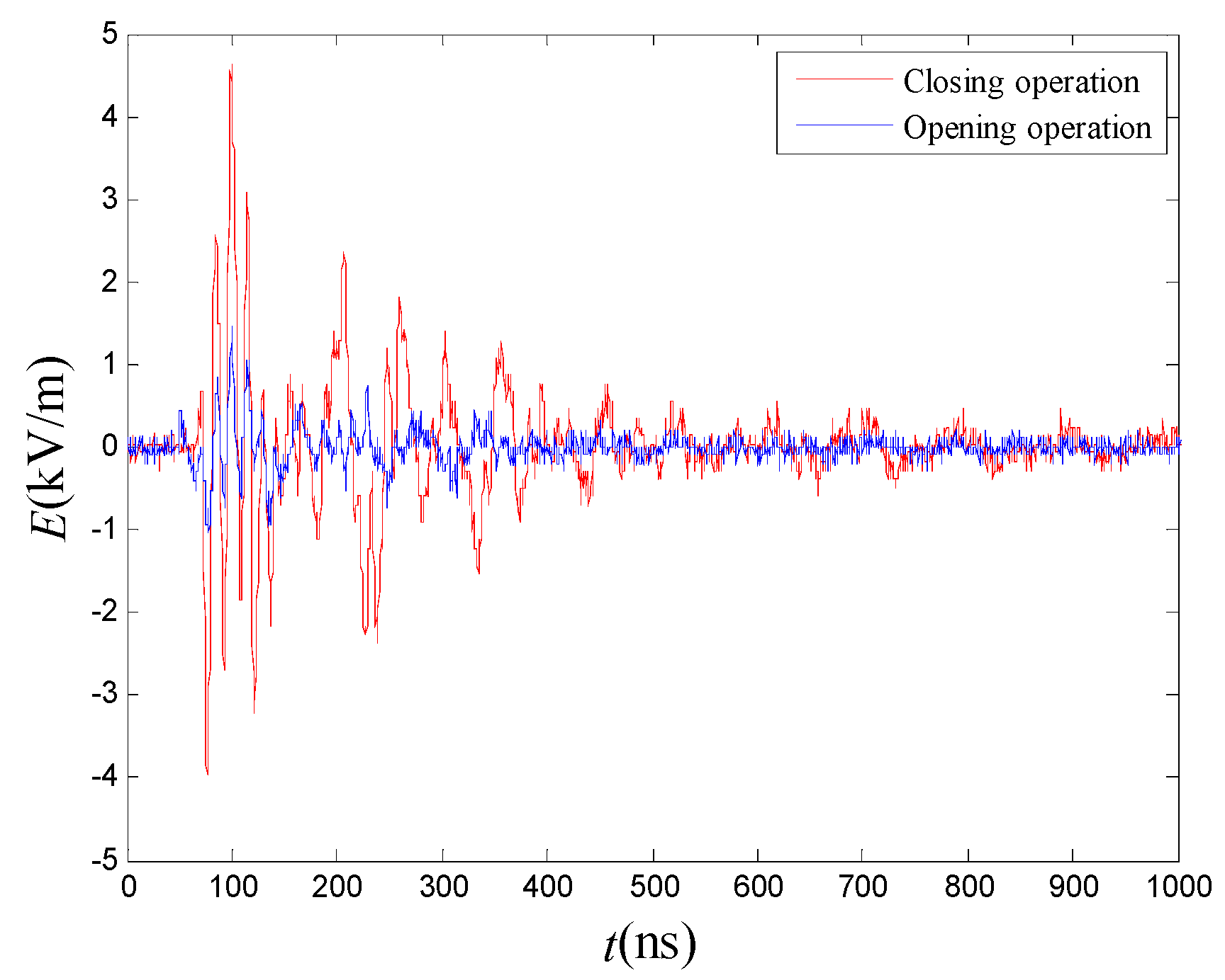
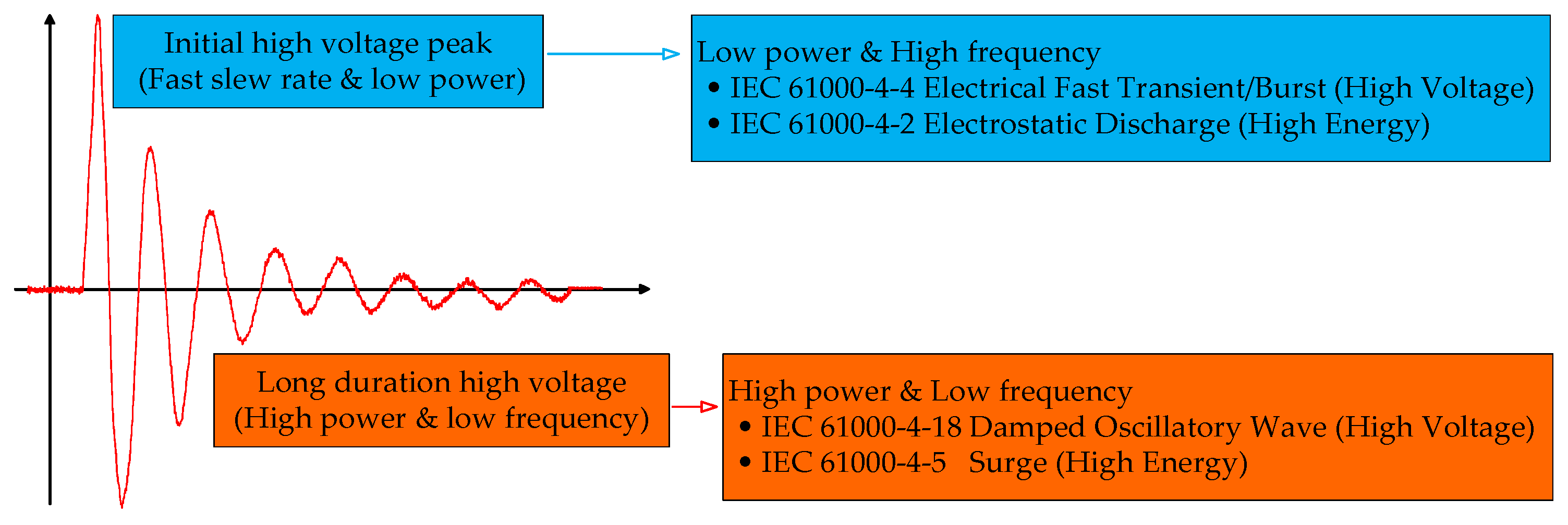
According to the actual operating status and experience in the test, the interference sources can be roughly divided into two categories. As shown in
Figure 13, one type is the interference with high frequency and low power, typical types of interference are electrical fast transient/burst (EFT) and electrostatic discharge (ESD). The other type is the interference with high power and low frequency, and typical types of interference are damped oscillatory wave (DO) and surge.
The above two types of interference sources often have relatively serious impacts on electronic equipment in actual environment and testing. These two types of interference can be classified into low power and high frequency, and high power and low frequency. For EFT, a set of fast transients has a sharp rising edge with high frequency, but the energy that the interference carries is relatively low. Similarly, the frequency of surge is low. On the contrary, surge brings high energy to the EUT, and it may damage the electronic devices. Hence, the tests of both two types of interference are arranged to compare the effects on the ECT acquisition card output waveform.
However, in the smart substation of the power grid, ESD often has a smaller impact on the secondary devices. Thus, this paper uses RF interference as a research object to replace ESD. Then, the test source includes both conduction and radiation, and the effects of the ECT output waveform after the disturbance will be studied. Next, this paper will couple RF interference, EFT, surge, and DO as interference sources to the ECT separately, and then evaluate the disturbed degree by the output waveform of the ECT.
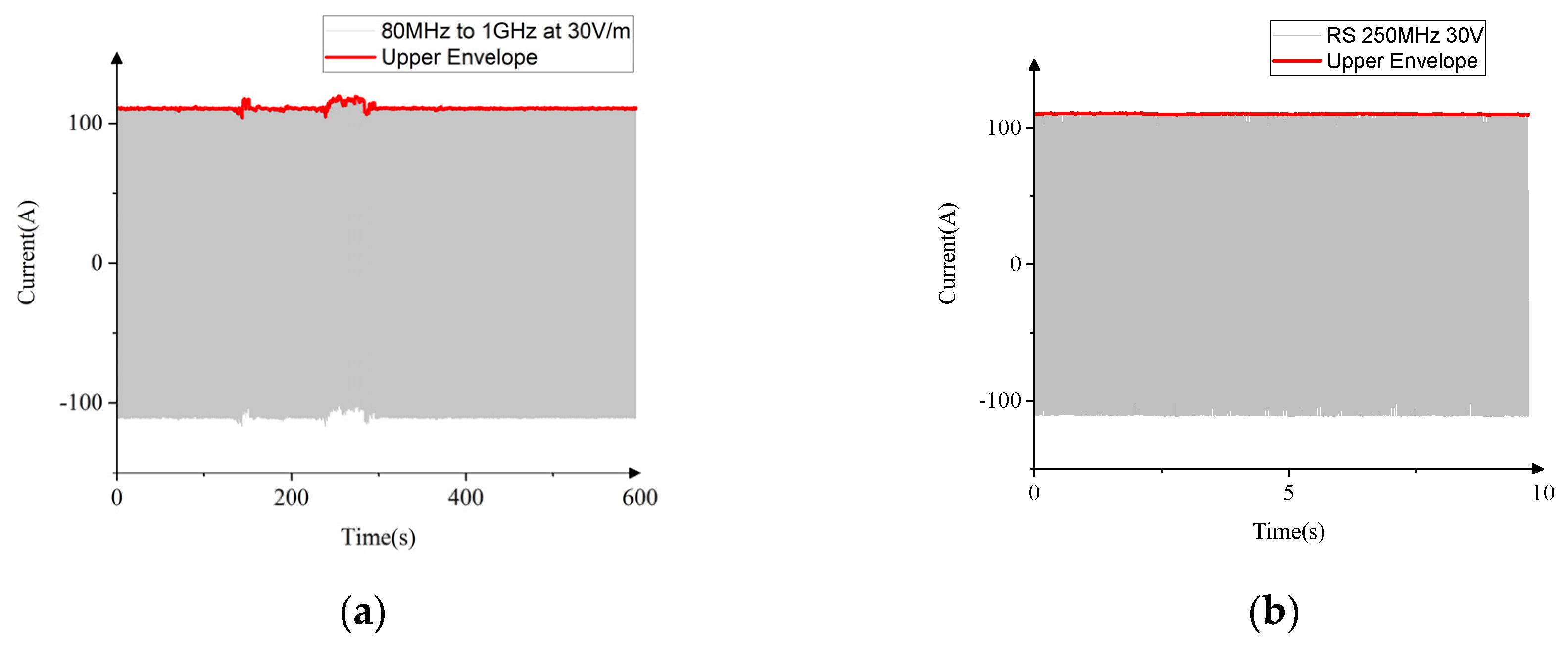
4.1. ECT Acquisition Card under RF
Radio frequency interference usually affects most electronic devices by radiated emission [
26,
27]. Such radiation’s frequency band includes small hand-held radio transceivers, stationary radio transmitters, television transmitters, in-vehicle radios and various industrial power supplies.
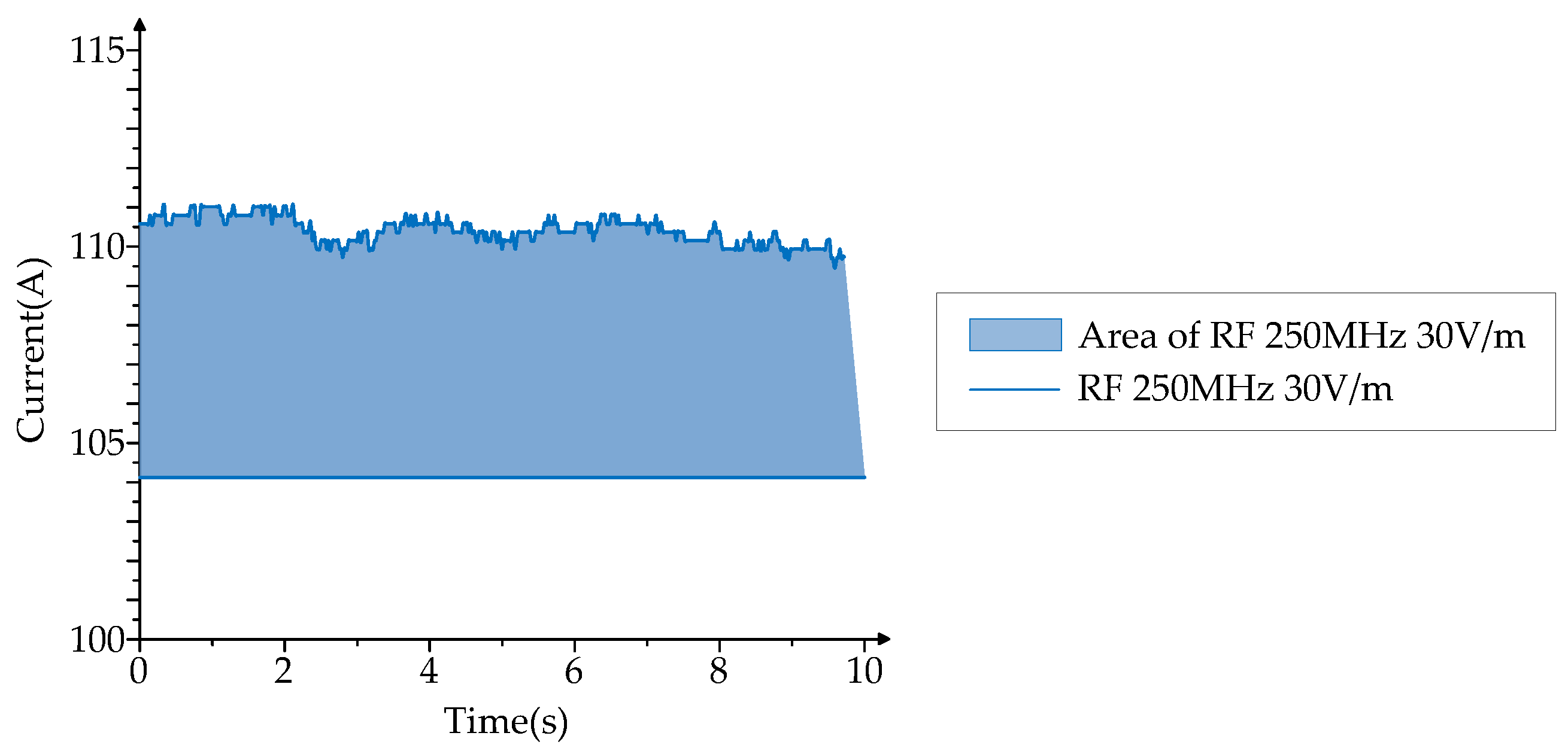
As discussed above, ECT output waveform under the RF interference at 250 MHz and an intensity of 30 V/m will be most impacted. We take this set of RF interference as the experiment parameter exerting influence on the ECT acquisition card.
Figure 14 shows the ECT output waveform envelope and its area of distortion (AD).
Calculating the data using Equation (19), the DD is 63 A·s. This DD reflects the impact of ECT after RF interference, showing that its output waveform is slightly shifted by approximately 6 amps in the overall positive direction. This can be explained that if the ECT is operating normally and there is a steady-state signal of an RF interference source nearby, the output waveform must be different from the waveform under normal conditions, which affects the accuracy of the collected data.
4.2. ECT Acquisition Card under Surge
According to the IEC 61000-4-5, surge is used to simulate a unipolar impact caused by a switch or lightning transient voltage [
28]. It has two types of transients, one is the power system switch transients and the other is lightning transients.
The power system switching transients can be caused by the power system switching operation, such as capacitor switching, partial switching operation or load changing in power distribution systems, resonance phenomena of switching devices such as thyristors, and system failures such as short circuits and electric arc.
The lightning transients are often caused by lightning, the main mechanisms are: (a) direct lightning, hit the outdoor transmission line, the injection of large current through the grounding resistor or generate voltage by external circuit impedance; (b) indirect lightning (i.e., EM fields generated by lightning strikes between or inside clouds, or lightning strikes on nearby objects), which generate induction voltages and currents in buildings and on external conductors; (c) a lightning current that discharges directly to the ground.
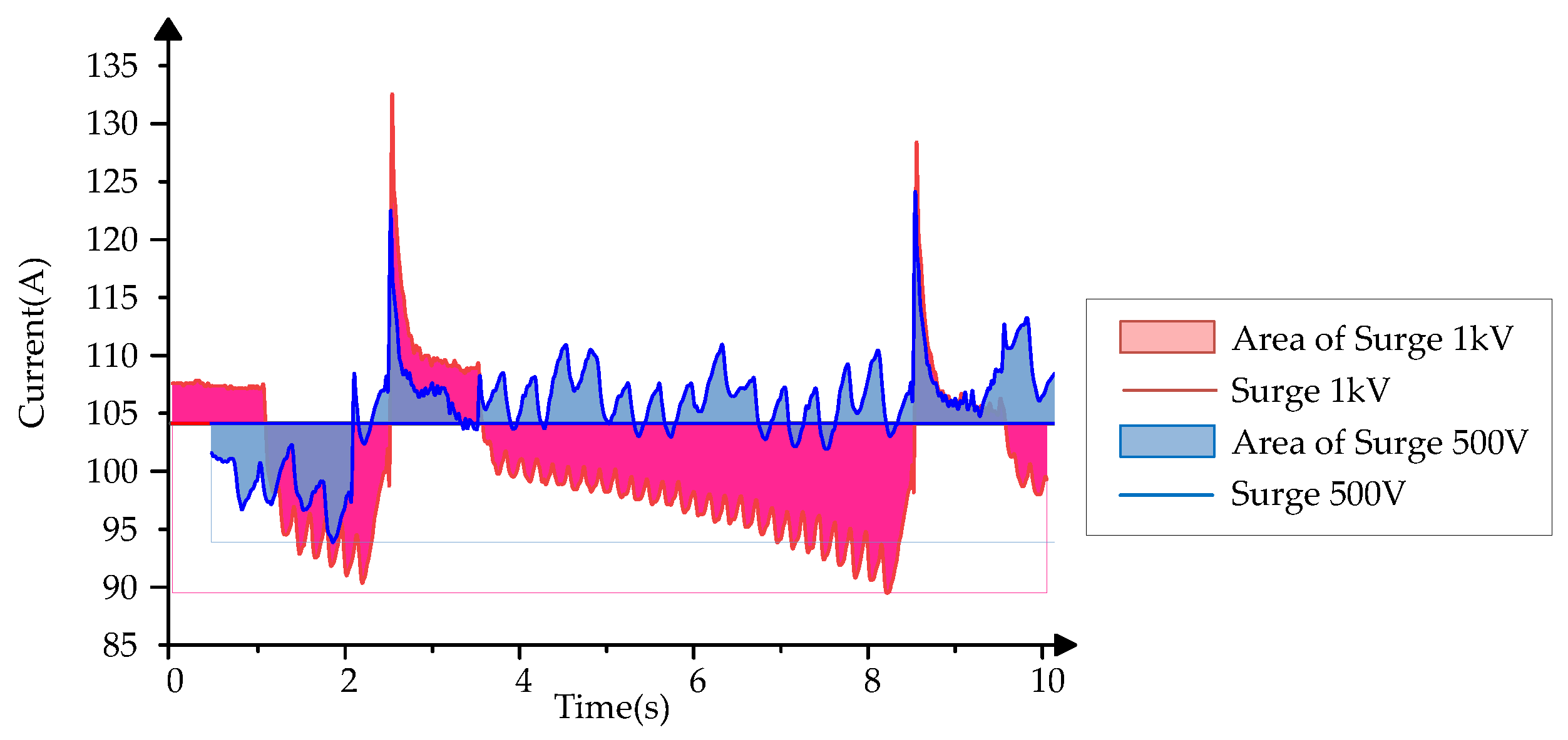
Figure 15 shows the AD of the ECT output waveform envelope under surge at 500 V and 1 kV.
Different to the RF, the ECT output waveform after surge immunity has a more pronounced distortion. When the first wave of the surge arrives, the ECT output waveform has an obvious spike (2.5 s). When this passes the half-peak time of the surge, the disturbed ECT output waveform will continue to fluctuate as the energy of surge decreases. Similar to RS, even if a cycle of surges (ms levels) has been completed, the ECT output waveforms still fluctuate, and the trend of volatility increases with the higher voltage level.
The output waveform of the ECT acquisition card, coupled with a 500 V surge, only fluctuated at the ordinate of approximately 104 amps. However, the output waveform of the ECT coupled with a 1 kV surge continued to decrease after the half-peak time, while the harmonics of a certain frequency continuously interfered with the hardware, causing the output waveform to shake continuously.
Calculating the data using Equation (19),
Table 3 shows the DD of the ECT output waveform under surge. As we can see, the disturbed fluctuation after the ECT acquisition card coupled with 500 V surge is greater than the disturbed fluctuation after coupling 1 kV surge, but it can be seen from
Figure 15 that the energy carried by the 1 kV surge shifts the output waveform of the acquisition card downwards, thus having a greater impact on the output of the ECT acquisition card. Therefore, it is not completely dependent on the number of the
DD to determine what kind of interference on the acquisition card has the greatest impact.
4.3. ECT Output Waveform under EFT
Electrical fast transient is a waveform group consisting of many fast transient pulses. EFT immunity testing is an experiment that couples EFT to power, control, signal, and ground ports for electrical and electronic devices. The experimental essential is a transient with high magnitude, short rise time, high repetition frequency and low energy. This test is intended to verify the immunity of electrical and electronic equipment to various types of transient harassment, such as the transient from switching operations (cut-off inductive loads, relay contact bounces, etc.).
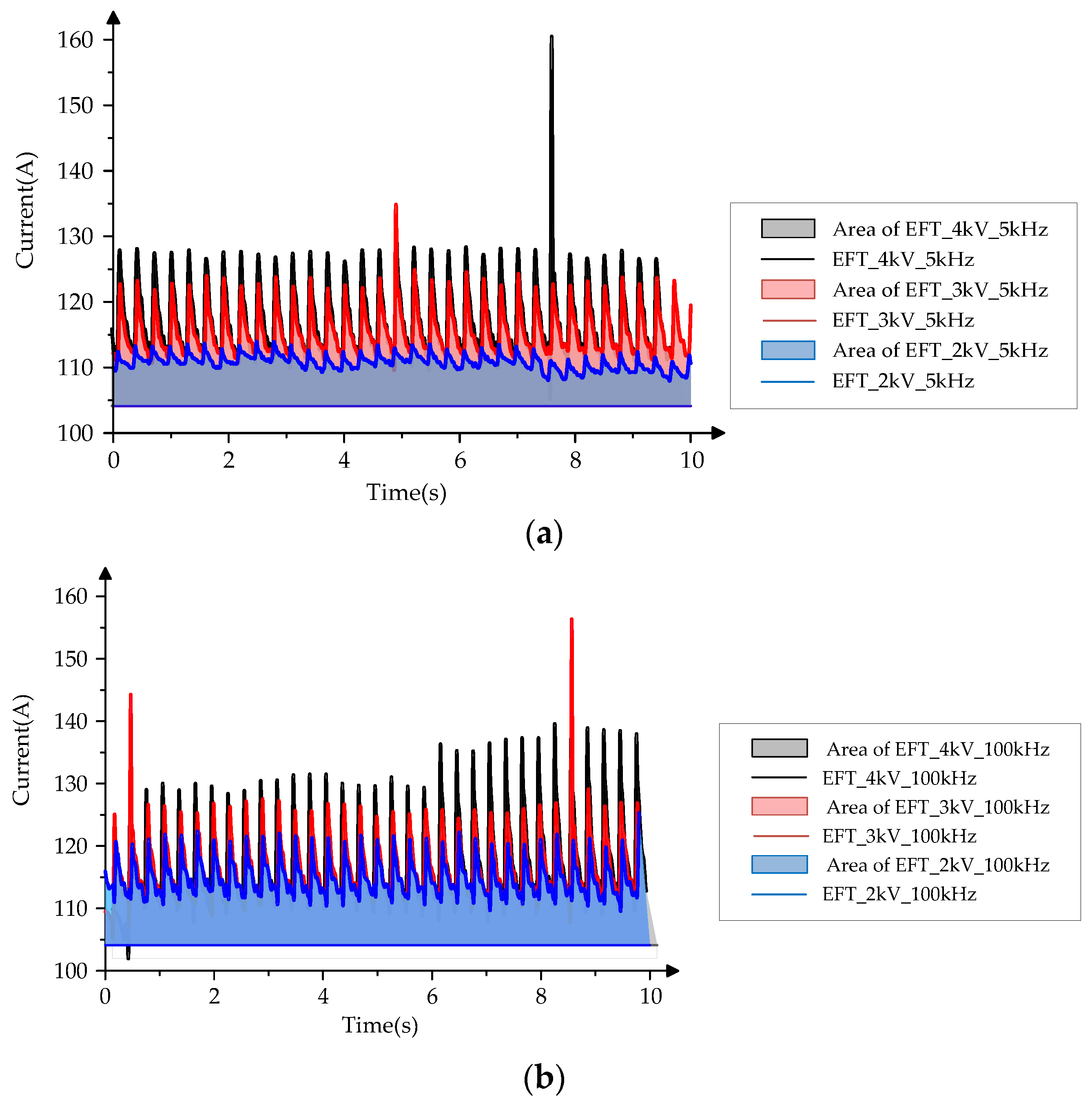
Figure 16 shows the envelope of the ECT acquisition card output waveform coupled with different frequency and voltage EFT, and the overall output waveform is “jagged”. According to the IEC 61000-4-4, the duration of the 5 kHz fast transient pulse is 15 ms and the duration of the 100 kHz fast transient pulse is 0.75 ms. Both cycles of 5 kHz or 100 kHz EFT are 300 ms, as shown in
Figure 16, with each “sawtooth” of the output waveform approximately 0.3 s. At the same voltage level, EFT at different frequencies also affects the output waveform of the ECT acquisition card. In the case of the same ordinate scale, under 2 kV EFT interference, 100 kHz has a greater impact on ECT than 5 kHz. For 4 kV EFT interference, the ECT output waveform distortion of 100 kHz is more than 130 A after 6 s, but 5 k Hz does not exceed 130 A except for one distortion spike.
Calculating the data using Equation (19) and shown in
Table 4, is the DD of the ECT output waveform envelope under different types of EFT. Unlike surges, the ECT output waveforms are offset in a positive direction by EFT interference, so the value of DD can indicate the degree of ECT disturbance directly. Compared to the 5 kHz EFT, the 100 kHz EFT has a greater impact on the ECT acquisition card.
4.4. ECT Output Waveform under DO
Damped oscillatory waves are mainly designed to meet the requirements and test methods of electrical and electronic equipment under switching operations. It includes:
First item DO appearing in power cables, control cables and signal cables installed in high-voltage and medium-voltage (HV/MV) substations.
DO in power insulated cables, control cables and signal cables of people and facilities mainly in gas-insulated substations (GIS) and in some cases, air-insulated substations (AIS) or due to high electromagnetic pulse (HEMP) oscillatory wave.
The phenomenon of DO can be divided into two parts. The first part is a slow-DO with an oscillation frequency between 100 kHz and 1 MHz. The second part is a fast-DO with an oscillation frequency above 1 MHz. The causes of these two types of DO are as follows:
Slow-DO represent the switching of disconnectors in outdoor HV/MV substations, especially those related to HV bus switching, and background noise in the factory.
Fast-DO’s specific environment is substations in the power grid, Fast-DO is produced by switchgear and control equipment.
An oscillation frequency of 1 MHz can be considered to represent the majority of cases, but for large HV substations, it is more appropriate to use 100 kHz as the oscillation frequency.
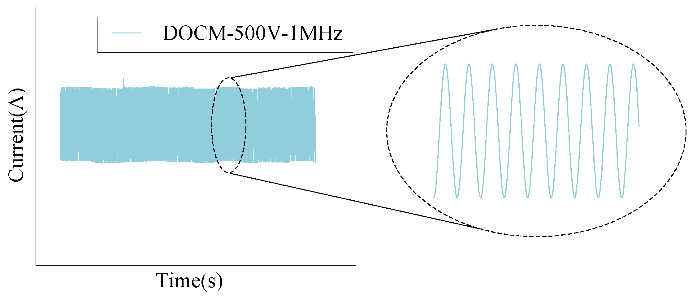
In this paper, we chose slow-DO representing the steep wavefront transients caused by operations of HV disconnectors in power stations.
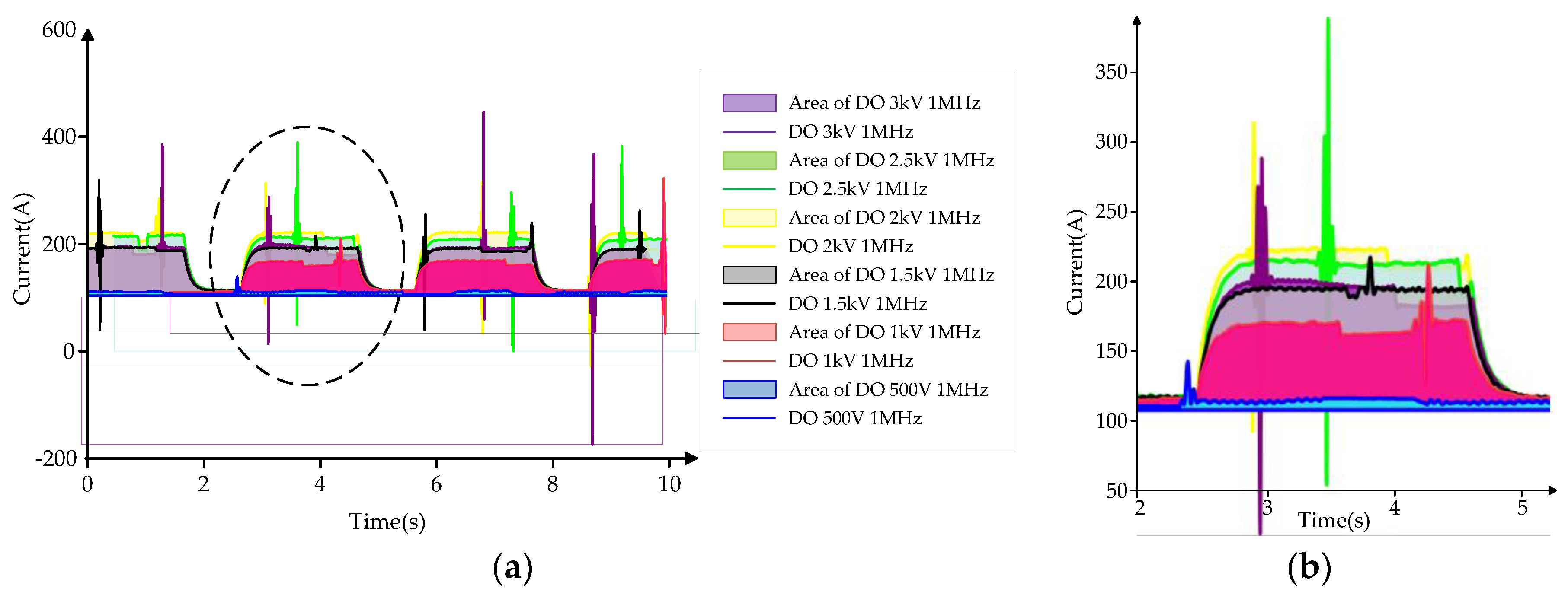
Figure 17 shows the envelope of the ECT acquisition card output waveform coupled with 1 MHz frequency DO and the voltage level range from 500 V–3 kV. We can see from (b) that the order of the AD of ECT output waveform after being disturbed is as follows: blue-red-black-purple-green-yellow. Unlike the expected positive correlation between DO voltage and output of disturbed ECT, the test results show that DO at 1 MHz frequency, when the voltage level is 2 kV, ECT is the most affected.
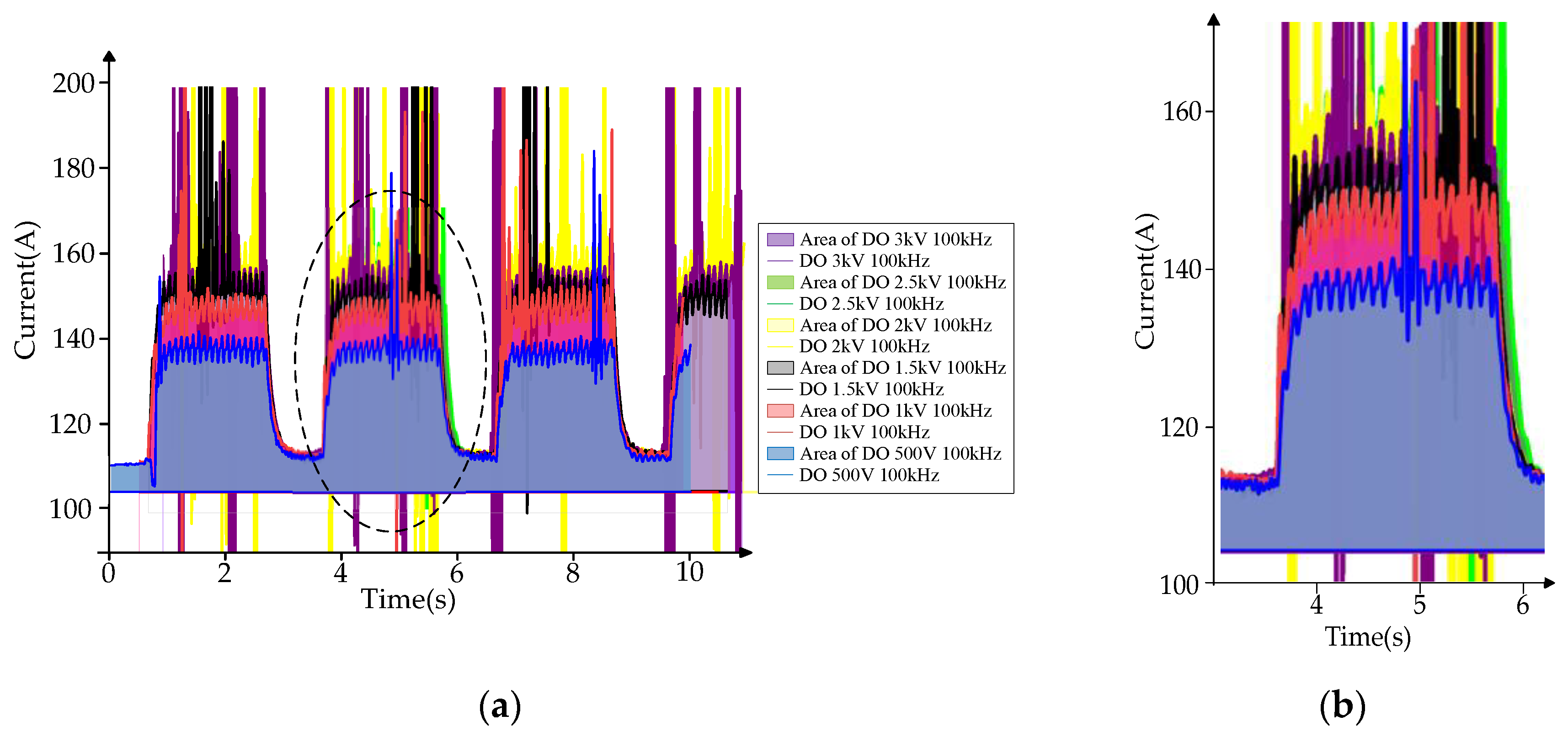
Figure 18 shows the output waveform of ECT after being disturbed by DO of 100 kHz.
We can see from the
Figure 18b that the order of AD of the ECT being disturbed is as follows: blue-red-black-purple-yellow. Because the output waveforms of green and yellow are similar, green may be blocked by yellow. Similarly, for the 1 MHz, when the voltage level ranges from 500–1500 V, the magnitude of the voltage level is positively related the interference level of the ECT, but when it reaches 2–3 kV, this positive correlation is invalid. The distortion in
Figure 18 is beyond the range of the coordinate axis, so the enlarged axis is shown in the
Figure 19.
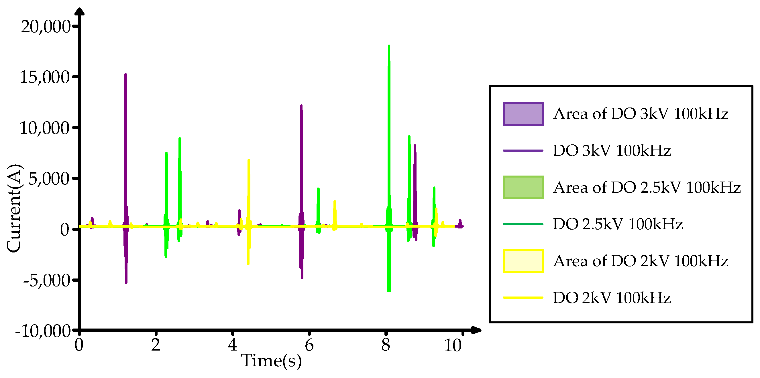
Figure 19 shows the output waveform of the ECT subjected to DO after 100 times magnification. Since 500–1500 V does not have much effect on the distortion of the ECT output waveform, in order to make the picture look clearer, only the effects of DO over 2 kV on the ECT output waveform are listed here.
Similar to the analysis above, as shown in
Table 5, the
DD of the output waveform after the ECT coupled with a voltage level of DO less than 2 kV has a positive correlation with the magnitude of the interference voltage. However, this positive correlation does not hold when it exceeds 2 kV.
At the same time, the influence of distortion peaks is compared between
Figure 17b and
Figure 18b. The most severe distortion after the disturbance in
Figure 18b is approximately 160 A. The curves in
Figure 17b, black, purple, green, and yellow are all around 200 A. It shows that, in most cases, the ECT received by DO of 1 MHz has a larger offset than the output waveform received by DO of 100 kHz. But, since 100 kHz DO is more likely to induce distortion peak of ECT output signal, the final calculated DD value between 100 kHz and 1 MHz has no regular pattern when compared.


