Article

Analysis of the Input Current Distortion and Guidelines for Designing High Power Factor Quasi-Resonant Flyback LED Drivers

1
Industrial & Power Conversion Division Application Laboratory, STMicroelectronics s.r.l, 20864 Agrate Brianza (MB), Italy
2
Istituto per la microelettronica e microsistemi, Consiglio Nazionale Delle Ricerche, 95121 Catania, Italy
3
Department of Electrical, Electronic and Computer Engineering, University of Catania, 95125 Catania, Italy
*
Author to whom correspondence should be addressed.
Energies 2020, 13(11), 2989; https://doi.org/10.3390/en13112989
Submission received: 7 April 2020 / Revised: 26 May 2020 / Accepted: 3 June 2020 / Published: 10 June 2020

Abstract

:
Nowadays, LED lamps have become a widespread solution in different lighting systems due to their high brightness, efficiency, long lifespan, high reliability and environmental friendliness. The choice of a proper LED driver circuit plays an important role, especially in terms of power quality. In fact, the driver controls its own input current in addition to the LED output current, thus it must guarantee a high power factor. Among the various LED drivers available on the market, the quasi-resonant (QR) flyback topology shows interesting benefits. This paper aims at investigating and analyzing the different issues related to the input current distortion in a QR flyback LED driver. Several effects, such as the distortion caused by the ringing current, crossover distortion due to transformer leakage inductance and crossover distortion due to the input storage capacitor have been experimentally reported. These effects, not previously studied for a high power factor (Hi-PF) QR flyback, have been analyzed in depth. Finally, some practical design guidelines for a Hi-PF QR flyback driver for LED applications are provided.

1. Introduction

Nowadays, almost a fifth of global electricity consumption is reserved for the lighting system [1]. As an example, in the USA, more than 200 billion kWh each year are expected for lighting systems, and the forecast confirms that the demand is going to increase in the next decade [2]. Traditional lighting equipment, such as incandescent lamps, florescent lamps and tungsten lamps, are environmental unfriendly, due to low efficiency or, in some cases, due to toxic substances that may contribute to the increase in ambient pollution levels [3]. In order to deal with these issues, many governments have already forbidden the trade of incandescent lamps and, on the other hand, encouraged the employment of light-emitting diodes (LEDs). They have been widespread both in private and public lighting systems thanks to their high luminous efficacy, long lifespan, high reliability and environmental friendliness [4]. Generally speaking, a LED lamp can be thought of as a combination of LED semiconductor materials and a driver circuit, thus the choice of the LED driver circuit plays a fundamental role from a power quality point of view. In fact, the driver controls both the LED output current and its own input current. Consequently, it must guarantee a high power factor (PF), and an input current with low total harmonic distortion (THD) [5,6]. Of course, it is worth remembering that LED lamps must comply with the national and international standards and regulations concerning harmonic currents, such as the standard IEEE-Std-519 and the IEC 61000-3-2.
LED drivers can be roughly grouped into “passive” drivers, since they use only passive components, and “switching” drivers, where there is at least a controllable power switch (e.g., a MOSFET) [7,8]. To further improve the quality of the switching LED drivers, a linear regulator could be added in series to the LEDs array. The linear regulator almost provides a dc output voltage and therefore, it eliminates the low frequency current ripple. Unfortunately, the aforementioned solution increases both the cost and worsens the efficiency.
The main drawback of passive LED drivers is the low PF that often cannot comply with the standard limit. Instead, switching LED drivers can realize a better output current regulation and higher power density, and they are more capable of satisfying the standard limits. Generally, there is a wide variety of LED driver topologies depending on the different power ranges. Furthermore, the topology of the driver can also be selected according to other requirements, including cost, galvanic isolation and efficiency.
The most common switching LED driver topologies for low and medium power applications are mainly based on single-stage (SS) or two-stage (TS) LED architectures. A SS LED driver consists of a dc-dc converter with constant output current regulation that also acts as a power factor correction (PFC). The SS LED drivers can be classified on the bandwidth of the feedback control systems. In the case of a narrow bandwidth (e.g., boost, buck-boost and flyback) the storage capacitor must be located at the output of the converter, otherwise it is placed between the two semi-stages (such as quadratic topologies) [9,10,11]. Although, the TS drivers consist of two power stages, where the first one acts as a PFC and the second stage performs output current regulation.
Focusing on the SS drivers, one of the main drawbacks is the bulky storage capacitor that also affects both the reliability and the size of the overall system. A PFC topology is usually adopted in the dc-dc stage to obtain high PF, and such a dc-dc stage is also responsible for setting the desired output current. In many of these applications, the power switches and control units are shared and embedded together to ensure a high reliability, efficiency and fast dynamics [12,13,14]. The reduction in the cost and size of the electronic ballast are additional benefits.
The flyback converter is the most used SS LED driver because it obtains high step-down ability and it provides a good tradeoff among the power quality, the cost, the capacitor size and the efficiency. In integrated lighting applications, a SS discontinuous current conduction mode (DCM) flyback PFC converter is commonly used to drive the LED lamps in order to achieve a high PF. The task is performed by means of a simple circuit configuration used to regulate the lamp current. A flyback LED driver operating in DCM where the PFC proprieties can be easily obtained has been frequently adopted. In this context, the quasi-resonant (QR) flyback LED drivers can effectively reduce the transformer size and weight thanks to the high switching frequency [15], which is not fixed since it increases as the load decreases. Furthermore, the switching losses can be strongly reduced by adopting zero voltage switching (ZVS).
This work aims at investigating and analyzing the different issues due to the input current distortion in a high power factor (Hi-PF) QR flyback LED driver. The THD performance of the whole converter is the result of the correlation of several causes such as the ringing current, crossover distortion due to transformer leakage inductance and crossover distortion due to the input storage capacitor. The input current distortion caused by the ringing current has been widely studied for the boost converter, while—as far as the authors know—it is the first time the problem has been studied for the QR flyback. Moreover, the crossover distortion due to the input storage capacitor in the case of a Hi-PF flyback LED driver has never been treated in literature. Finally, an accurate analysis is performed in this paper by considering the linear approximation of the input voltage and the related comparison with a sinusoidal waveform.
The paper is organized as follows: In Section 2, a classification of several LED drivers is introduced, and their main characteristics are discussed. The main issues related to input current distortion in a Hi-PF QR flyback converter are discussed in Section 3. In Section 4, some practical design guidelines for a Hi-QR flyback driver for lighting applications will be discussed, along with a few experimental results.

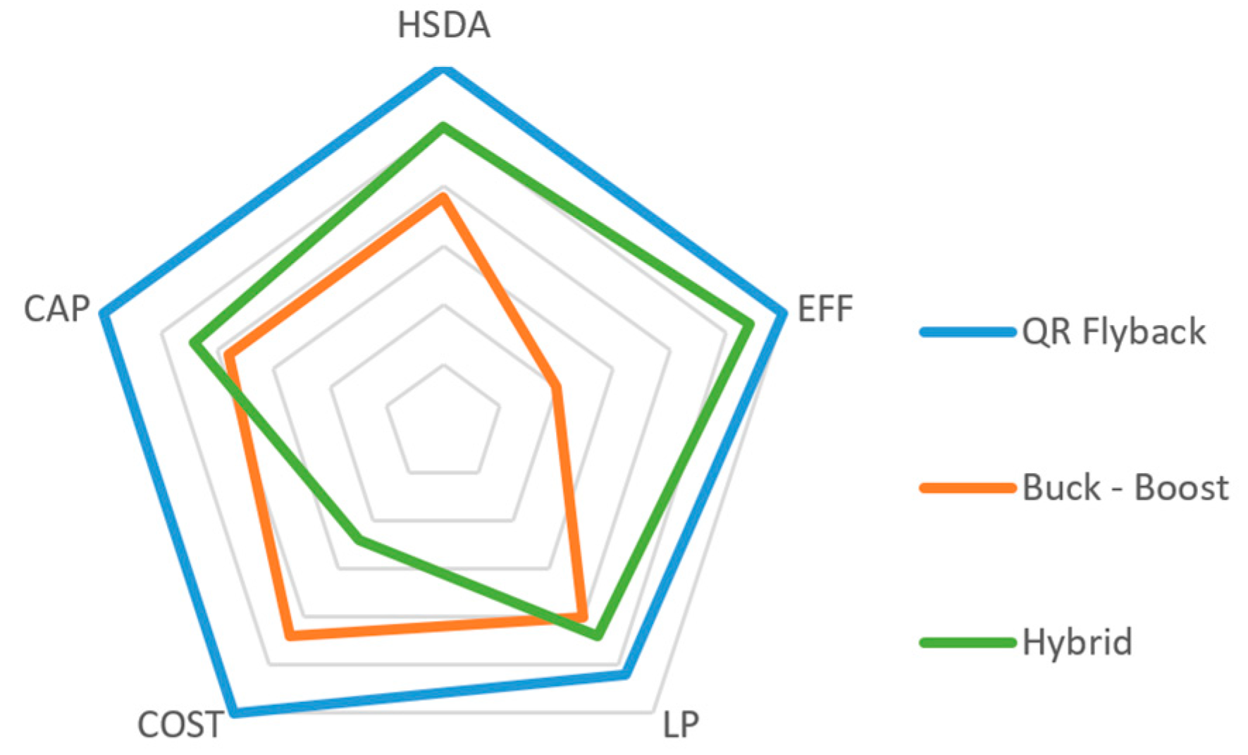
2. Brief Overview of LED Driver Topologies

In this section, various topologies of passive and switching LED drivers are described and classified. The passive drivers are simpler and more reliable and they operate at the line frequency. No active control is developed, so a significant current ripple can occur. The switching drivers can strongly reduce the current distortion and improve the PF with the additional advantage of being suitable for high frequency operations, thus enabling reduced size. On the other hand, switching LED drivers are less reliable than passive ones.

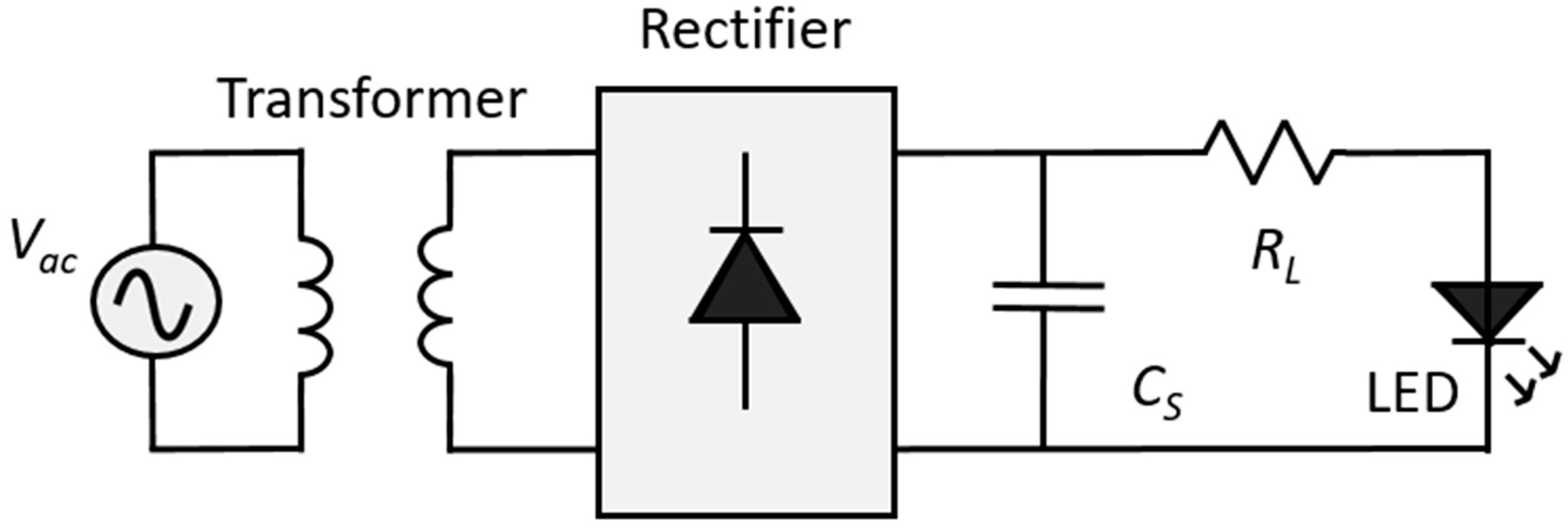
2.1. Passive LED Drivers

Passive LED drivers are characterized by the exclusive use of passive components (e.g., resistors, capacitors, magnetic components). The insertion of an impedance between the ac line and the LED lamp load to limit the current is mandatory. One of the main drawbacks of these topologies is the low PF and high THD, which are sometimes not enough to meet the standards [16].
Passive LED drivers can be classified into lossy and lossless impedance drivers. The strength and simplicity of the lossy impedance driver is due to the use of a resistor RL or a linear regulator on the dc side, as depicted in Figure 1. In many practical applications, it is widespread to use a bulky step-down transformer from high to low voltage. It has two-fold benefits—it reduces the voltage drop on the resistor with an increase in the overall system efficiency and, at the same time, guarantees galvanic isolation. A large electrolytic capacitor CS is typically used in order to avoid flickering.
A passive driver with a lossless impedance (an inductor, capacitor or their combinations), usually placed in the ac side to limit the LED output current, is shown in the example in Figure 2. An inductor Lin is usually adopted with the aim of replacing the less efficient and low-frequency transformer. The Lin usually behaves as an additional input filter (by means of Cin) which smooths the input current and leads to advantages such as reducing the input current distortion [17,18,19]. Instead of using a bulky electrolytic capacitor (E-CAP) that ensures a constant output current, a non-E-CAP is often used on the dc side, still achieving a higher PF with respect to the lossy counterpart. This solution can ensure a longer lifetime and smaller size of the overall system, although there is a small output current ripple in the LED load. Notwithstanding, lossless passive drivers can reach high efficiency, above 90% [18].
Passive drivers can be easily employed in outdoor applications and they are very cost effective, especially for low-power applications. The main drawbacks of passive LED drivers are their lack of a proper output current control and their having an input current THD that does not always meet the standards target.

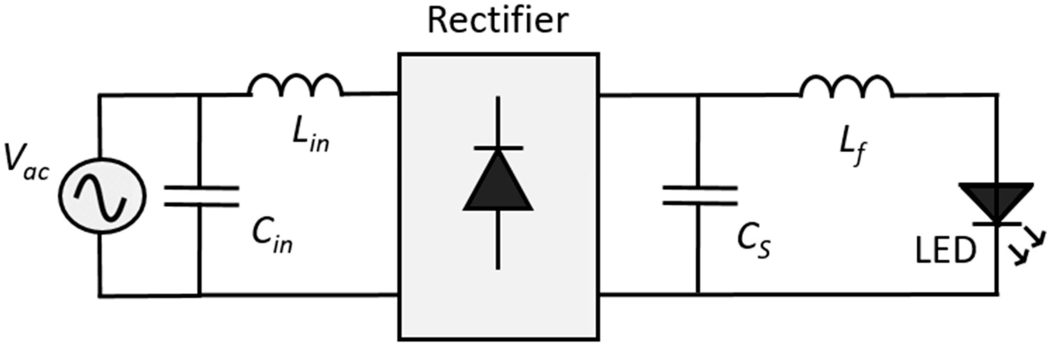
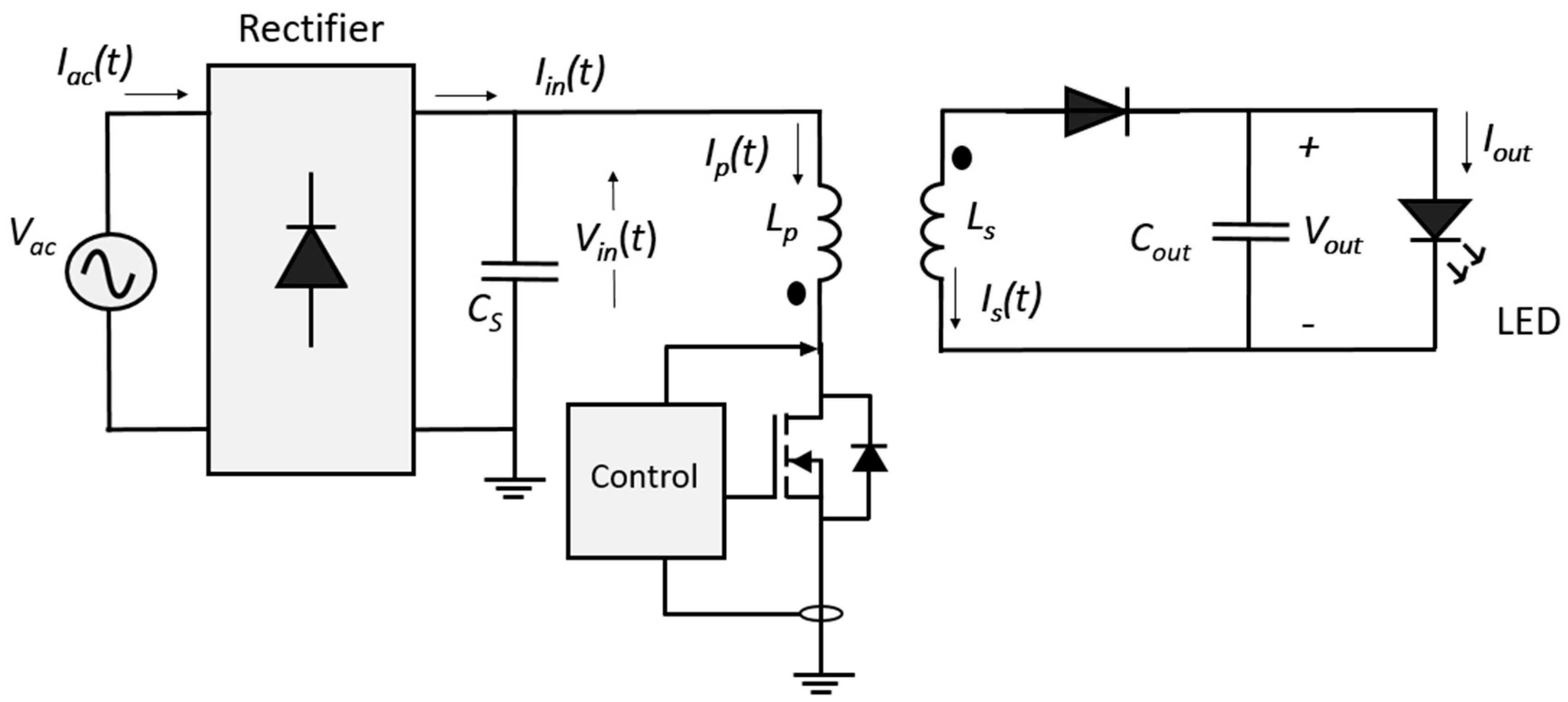
2.2. Switching LED Driver

Switching LED drivers bring various advantages arising from the use of the switching devices. Moreover, switching LED drivers can embed into a single electronic ballast with various functionalities, such as circuit fault protection and active and high PFC [20]. They are especially employed in indoor applications, since the whole circuit control is compact, reliable and effective with a low and controllable ripple output current. Another strength point of switching LED drivers is their higher efficiency in comparison to the passive ones. Switching LED driver topologies can be classified into two main categories, SS and TS, as shown in Figure 3. The SS drivers consist of a single power stage that acts as both a dc-dc regulator and PFC, shown in Figure 3a, with a storage capacitor Cs. On the other hand, the TS drivers are used for high-power applications. The aforementioned drivers comprise two power conversion stages that can perform different functions. In general, the first stage acts as a PFC and the second one as a dc-dc regulator and filter [21], as depicted in Figure 3b.
In the following section, there is a brief focus on SS LED drivers with the main advantages of different topologies adopted in the literature.
SS drivers usually have a low component count and among them a power switch that controls a power conversion stage. However, it is often difficult for a SS driver to simultaneously ensure good performance in many respects, such as high efficiency, high PF, constant current output and so on. SS drivers are suitable for low and medium power class applications (below 70 W) where size and cost are usually more critical than PF and efficiency. The storage capacitor is usually placed downstream from the dc-dc converter, that is on the high frequency side, as shown by the red capacitor in Figure 4, to obtain a high PF. Notwithstanding, another approach can be found in some embedded LED drivers where the capacitor is placed on the low frequency side, as shown by the blue capacitor in Figure 4. More specifically, such an approach has sometimes been used in very low power applications (below 5 W) [22]. Indeed, nowadays, in this power range, passive LED drivers are adopted to guarantee an inexpensive cost. Figure 5a shows the waveforms of the current drawn by LED lamps when the capacitor is placed on the low and high frequency side. The waveforms confirm that the dc-dc converter can guarantee PFC only when the storage capacitor is placed downstream from the dc-dc converter itself. Although the input current drawn by the LED lamp has a better THD when the capacitor is placed at the high frequency side, a higher output current ripple occurs in comparison to the previous solution, as shown in Figure 5b. However, the required storage capacitance is not always able to handle both the low and the high frequency ripple [23].
The SS LED drivers can be roughly classified on the bandwidth of the feedback control systems. In the case of a narrow bandwidth (e.g., boost, buck-boost and flyback) the storage capacitor must be located at the output of the converter. Instead, in the case of a wide bandwidth system (e.g., quadratic or single-stage single-switch input current shaper topologies) the storage capacitor is placed between the two semi-stages. In the following, the narrow bandwidth systems have been analyzed. In detail, a huge number of conventional LED drivers are widely discussed in literature, such as buck [24,25,26], buck-boost [27], SEPIC [28,29], flyback [30,31], half-bridge [32,33,34] and push-pull converters [35,36]. Furthermore, PFC can be achieved with valley-fill circuits [37]. Other approaches, such as coupled-inductor modified converters [38,39,40,41] and valley-fill modified converters [42], show a simple solution to the step-down ratio requirement without compromising the efficiency and system complexity.
The flyback converter has been widely adopted in LED driver lamps because of its simple structure and high PF. One of the strengths is its efficiency, which can be improved by using the leakage energy or using soft-switching techniques [43]. In spite of the flyback LED driver having various advantages, in many practical applications the QR mode operation has become one of the most familiar methods in LED driver applications. It is worth noting the decrease in switching losses with respect to a flyback converter operated with a fixed frequency. Moreover, the QR driver has an enhanced transient response in DCM operation [44,45] and it may have a smaller EMI filter [46]. In fact, in applications operated from the mains, the switching frequency is modulated at twice the mains frequency due to the voltage ripple appearing across the input capacitance. The switching frequency span depends on the amplitude of this input voltage ripple. This causes the spectrum to be spread over some frequency bands, rather than being concentrated on single frequency values.
In addition, the QR driver has a higher safety degree under short circuit conditions, since the switch is not enabled until the primary windings are fully demagnetized. Therefore, transformer saturation is not possible. On the other hand, the QR flyback LED driver may have a high ripple output current and high conduction losses in comparison to the fixed frequency driver.
It is important to point out that the difference between a DCM flyback and a QR flyback is in the turn-on mechanism. In a DCM flyback converter, the gate driver provides a constant switching frequency, while in a QR flyback a variable frequency is used, where the off time depends on the resonant valley detection of the drain-to-source voltage ringing that follows transformer demagnetization. Figure 6 depicts the drain-to-source voltage waveforms in the case of a DCM flyback, shown in Figure 6a, and a QR flyback, shown in Figure 6b, thus highlighting the benefit in terms of reduced switching losses.
A simplified schematic of a QR flyback LED driver (not for Hi-PF applications) is shown in Figure 7. The primary current Ip starts to flow into Lp when the power switch is turned on. The voltage at the secondary is such that the diode is reverse biased, hence the capacitance Cout supplies the LED string. Once the switch is turned off, the current Ip goes to zero and the voltage across both windings reverses, so that the output diode is forward-biased. Then, the current starts flowing in the secondary winding and Cout can be charged by the energy stored in the transformer. It is worth noting that, while the current flows on the secondary side, the drain–source voltage is equal to the rectified input Vin(t) plus the reflected output voltage VR at the primary windings. The transformer takes a time TFW to demagnetize, and as soon as the energy transfer is completed, the drain–source voltage starts ringing. The main reason for this energy exchange phenomenon is due to a resonant tank between the inductance Lpp and the capacitance Cpp. The inductance Lpp is the sum between the leakage inductance of the copper paths and the primary winding Lp. The latter it is the prevalent contribution, hence Lpp can be simply approximated as Lp. The capacitance Cpp can be expressed as the sum of the parasitic capacitances on the primary circuit and the capacitances of the secondary circuit referred to the primary one. The latter are due to the parasitic capacitances of the secondary circuit and to the output capacitance Cout. The primary circuit capacitance includes various contributions: the output parasitic capacitance Coss of the MOSFET; the junction capacitance of the diode; the package capacitance; the intra-winding capacitance of the transformer; plus other stray contributors together and so on [47,48,49,50,51]. Coss is a strongly nonlinear capacitance and, especially in the latest MOSFET generations, it increases dramatically (100 times or more) when the drain–source voltage, vDS, falls below few tens volt; i.e., Cpp is a function of vDS: Cpp(vDS). In the following, this capacitance will be considered constant or, at least, not significantly impacting the overall CDS. Hence, the resonant frequency fr can be represented as:
f r = 1 2 π L p p C p p ( v D S ) 1 2 π L p C D S
In applications, the inductance Lp is measured with an impedance meter or by measuring the di/dt when a voltage square wave is applied, while CDS is esteemed by Equation (1) from the measurement of the drain–source voltage ringing.
Bearing in mind that, in a conventional QR topology a feedback voltage loop is used, and this loop controls the average value of the secondary current Is, it follows that the switching frequency is continuously adjusted depending on the output current load. In this way the switching device turns on when necessary, provided that the inner controller is able to detect a valley in the ringing drain–source voltage. The switching period T can be expressed as:
{ T = T o n + T F W + T r i n g T r i n g = 1 2 [ 1 + 2 ( k 1 ) ] T r
where Ton is the on time of the power switch, TFW is the time interval where the current flows on the secondary side and Tring is the time interval during which the drain–source voltage rings. Ton is reduced as the load reduces, hence at very light load the frequency is high. Therefore, the maximum switching frequency imposes a minimum Ton. In this case, a further load reduction involves an increment of Tring. In detail, Tring strictly depends on the load level and it is imposed by keeping off the switch for some valley points in the drain–source voltage. In other terms, it depends on the number of the valley points k “skipped” by the controller. More specifically, k increases as the load level decreases. The term k is equal to 1 until Ton is greater than its minimum value, i.e. the switch is turned on at the fist valley on the drain–source voltage waveform (one-half of the resonant period). Thus, the QR mode operation of the converter represents the condition k = 1.
The reason behind the turn-on during a valley point of the drain–source voltage is the achievement of lower capacitive switching losses:
E s = 1 2 C D S V D S 2
This mechanism is able to minimize in a significant way the switching losses. It is worth noting that the bill of material of a QR driver contains only a few simple components, which implies an inexpensive solution [51,52].
Finally, Figure 8 compares the performance between a QR flyback, a buck-boost and a hybrid solution [36,37,38,39,40,41,42,43,44,45,46,47,48,49] in terms of some key factors. The high step-down ability (HSDA) [36,37,38], efficiency (EFF) [38,39,40,41], compact capacitor volume (CAP) [42], cost (COST) [43,44,45,46] and low power range applications (LP) [47,48] have been taken into account for the three converters. The comparison highlights the superior performance of the QR flyback converter, which makes it the preferred choice for LED driver applications.

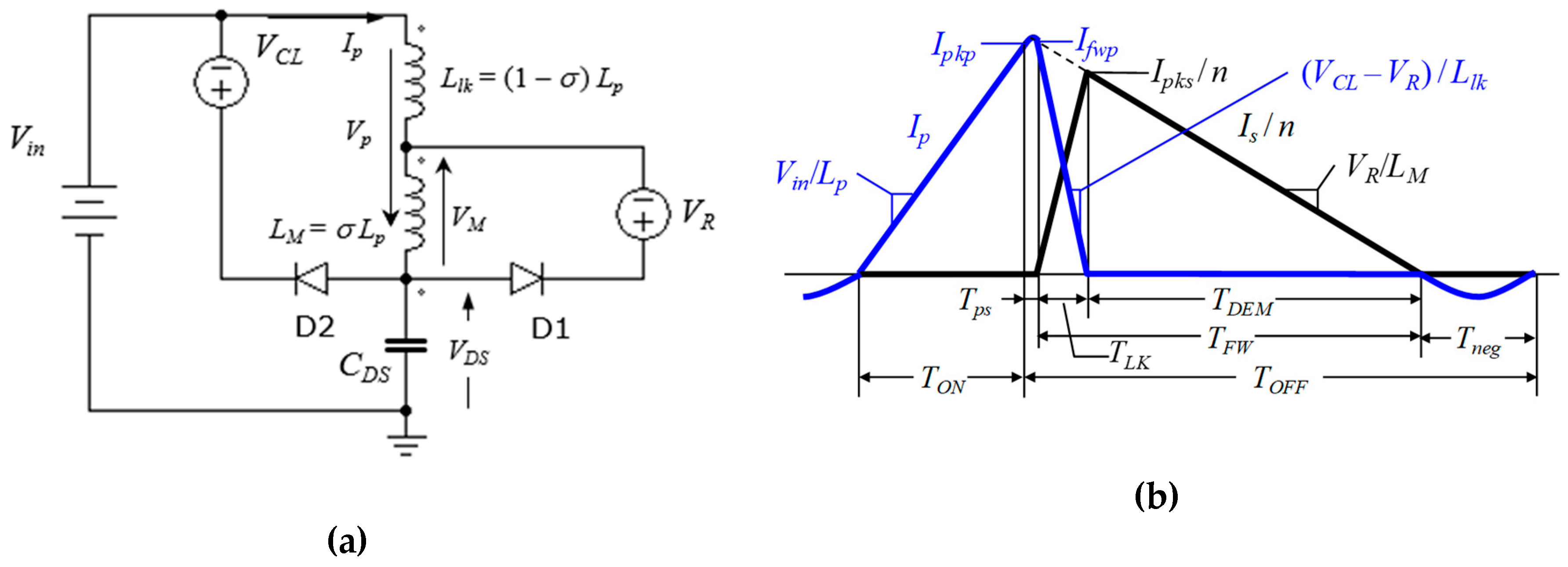
3. Analysis of Input Current Distortion due to Power Processing and Power Circuit

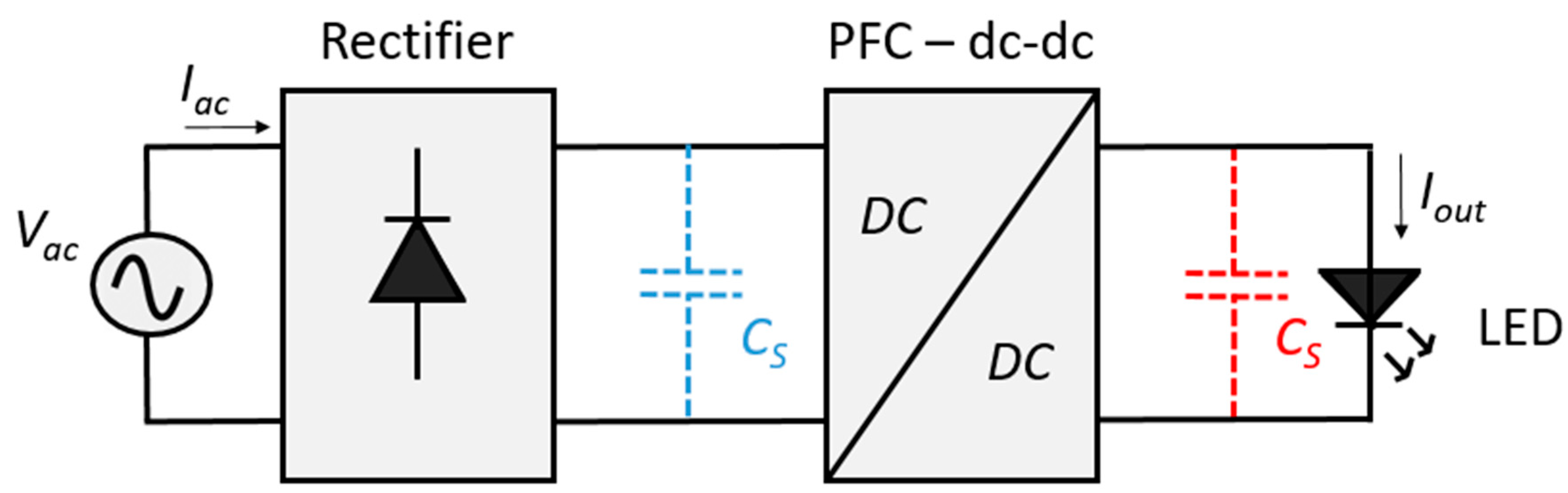
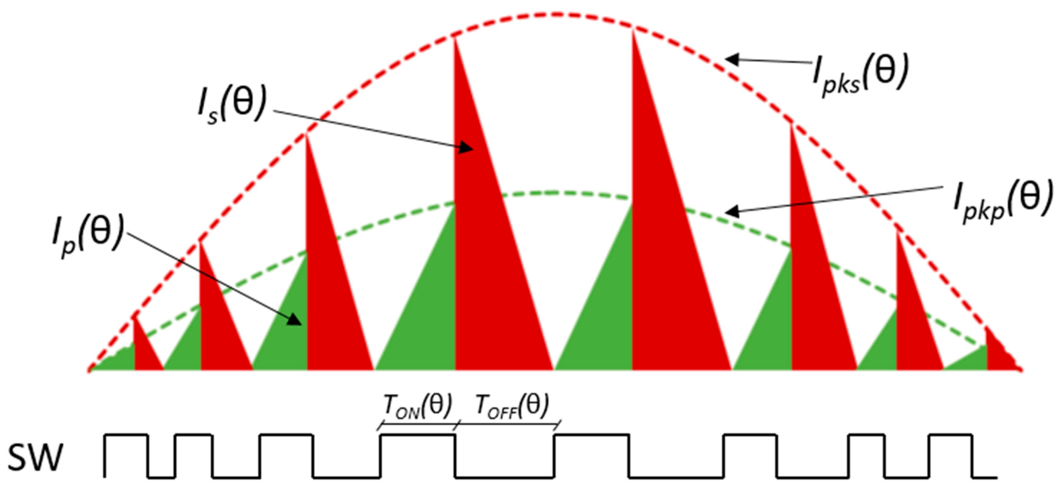
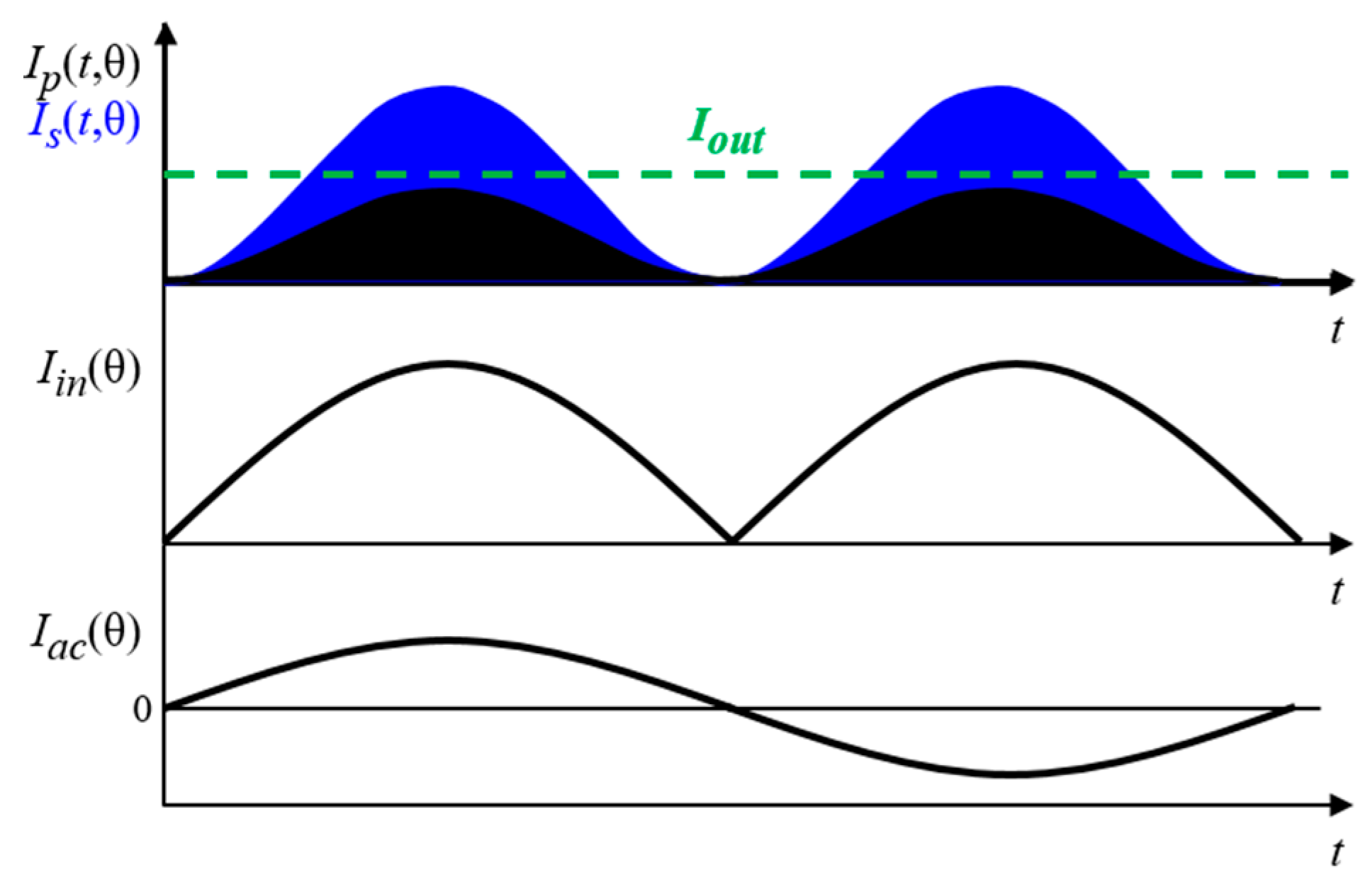
3.1. Generic Control Method Obtaining High Power Factor

Although the QR flyback converter topology is extremely popular since it is a very cost-effective solution with high performance, the converter features inherent distortion of the input current [48]. Normally, this distortion is not a concern for compliance with the IEC61000-3-2, however, some input current THD targets (e.g., <10% at full power) are becoming market requirements that are very difficult to achieve, especially when working with lighting equipment over 25 W [53].
As shown in Figure 7, the storage capacitor of the QR flyback is placed on the low frequency side of the dc-dc converter. With the aim to reduce the input current THD, the capacitor should be placed downstream from the converter, according to the waveform simulations in Figure 5a (red trace) related to the capacitor position of Figure 4. In this perspective, the converter can be considered as a Hi-PF QR flyback, which has a rectified voltage in input and the storage capacitor downstream of the power stage. The aforementioned solution strongly reduces the harmonics distortions of the input current drawn by the LED lamp.
The control gear in a Hi-PF QR flyback converter has a twofold task: firstly, it is responsible for regulating the output voltage or current and, simultaneously, it has to maintain a low THD of the input current. For the sake of completeness, the characteristics and proprieties of the control method that have to be considered to achieve a Hi-PF QR flyback converter will be briefly discussed.
The control method, shown in Figure 9, is responsible for the turn on and turn off of the switch.
Henceforth, the quantities depending on the instantaneous line voltage will be considered as a function of the term θ = 2πflinet.
The target of the control method is to obtain an input current very similar to a sinusoid in-phase with the input voltage to achieve high-PF. Regardless of the specific control method, the previous target can be partially converted into obtaining a primary current, as shown by Ip in Figure 7, whose peak envelope, detailed by the green elements in Figure 9, leads to a sinusoid in-phase with the input voltage. To obtain such an envelope, the control method must turn off the switch when the current on the primary side reaches one of the (green) peaks in Figure 9. To obtain a similar result for the secondary current, shown by the red elements in Figure 9, a similar control must be adopted for the switch turn on. The turn on must occur when the transformer is fully demagnetized, thanks to a zero-current detector. In other terms, the combination of these switching rules, which result in a variable switching frequency, shown in Figure 9, ensures that the peaks of the primary current, in a half period of the rectified voltage Vin(θ), can be enveloped by a rectified sinusoid. The primary current Ip(θ) in a switching cycle is triangular shaped and flows only during the switch on-time, as sketched by the green triangles shown in Figure 9. During the off time, the secondary current Is(θ) flows and it is represented by the red triangles. Therefore, the switching frequency SW is variable, where the TON(θ) and TOFF(θ) are modulated to achieve a sinusoidal current envelope.
However, the primary current Ip(θ) flows only during the on-time of the power switch, and this means that the average value of the primary current deviates significantly from an ideal sinusoid. To ensure good performance and low THD input current for a Hi-PF driver LED, the quantity D2T (D is the duty ratio) must be constant along each line half-cycle, thus a unity PF is obtained [54].
In this paper, it is assumed that the generic control method implements the previous features. For the sake of simplicity to obtain a quantitative expression of the input current Iin, the following assumptions have been considered:
  • The line voltage is sinusoidal, and the input bridge rectifier is ideal, thus the voltage at the bridge output terminal is a rectified sinusoid.
  • The voltage drop across the power switch in the on-state is negligible and there is negligible energy accumulation on the dc side of the bridge.
  • The transformer windings are perfectly coupled (i.e., no leakage inductance).
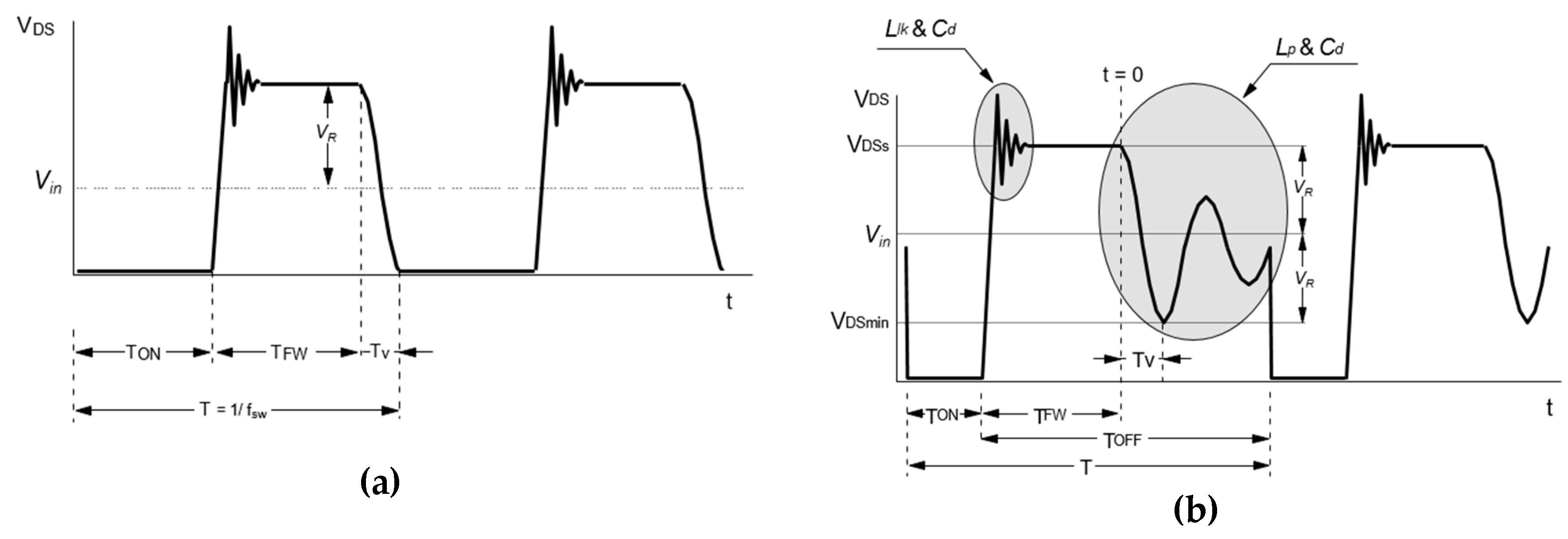
  • The turn-off transient of the power switch has negligible duration so that TFW immediately follows TON.
  • The converter is operated so the power switch is turned on in each cycle after the secondary current becomes zero, therefore in either QR-mode (i.e., on the first valley of the ringing in the drain–source voltage) or DCM.
  • The output voltage is constant along a line half-cycle.
  • During the time interval elapsing from the instant when the transformer demagnetizes to the instant when the power switch is turned on, the transformer current is zero; consequently, the initial current during the on-time is zero too. This time interval is equal to Tr/2 in the case of the converter being used in QR mode.
It is worth generalizing the relation to D2T when a variable switching frequency is used, in particular:
D 2 T = [ T O N ( θ ) T ( θ ) ] 2 T ( θ ) = T O N ( θ ) 2 T ( θ ) = constant
where the dependences of TON and T on θ point out that they are a function of the instantaneous line voltage Vac. Assuming that the rectified voltage Vin is sinusoidal in 0 ≤ θ ≤ π, according to assumption 1, it can be written as:
V i n ( θ ) = V i n , p k sin ( θ )
where Vin,pk is the amplitude of the rectified voltage.
By considering the current flowing in the primary windings during the time interval TON, and bearing in mind the inductance current–voltage differential relation, the peak value of primary current Ipkp(θ) can be expressed as:
I p k p ( θ ) = 1 L p ( V i n , p k sin ( θ ) ) T O N ( θ )
The generic control method must ensure that the height of the triangles depicted in Figure 9 varies along a line cycle as expressed by Equation (6). To reach this target, the control method must properly vary the width of TON(θ) as well as TOFF(θ). The input current Iin(θ) is the average value of each triangle over a switching cycle, hence, taking Equation (6) into account:
I i n ( θ ) = 1 2 I p k p ( θ ) T O N ( θ ) T ( θ ) = 1 2 L p ( V i n , p k sin ( θ ) ) T O N ( θ ) 2 T ( θ )
It is worth noting that, if the ratio Ton(θ)2/T(θ) is maintained constant by the controller, the input current Iin(θ) can be assumed sinusoidal. Figure 10 summarizes the key current waveform in the Hi-PF driver LED.
Despite the fact that a suitable control method leads to a Hi-PF QR flyback driver according to the previous features, there are different inherent causes of distortion in the input current to be faced. The distortion due to these causes is reported in the next section where the THD has been experimentally evaluated. After that, in the following subsections, these causes, due to the power processing mechanism of the QR flyback converter that are not ascribable to the specific control method (although the control method may mitigate them), are described.

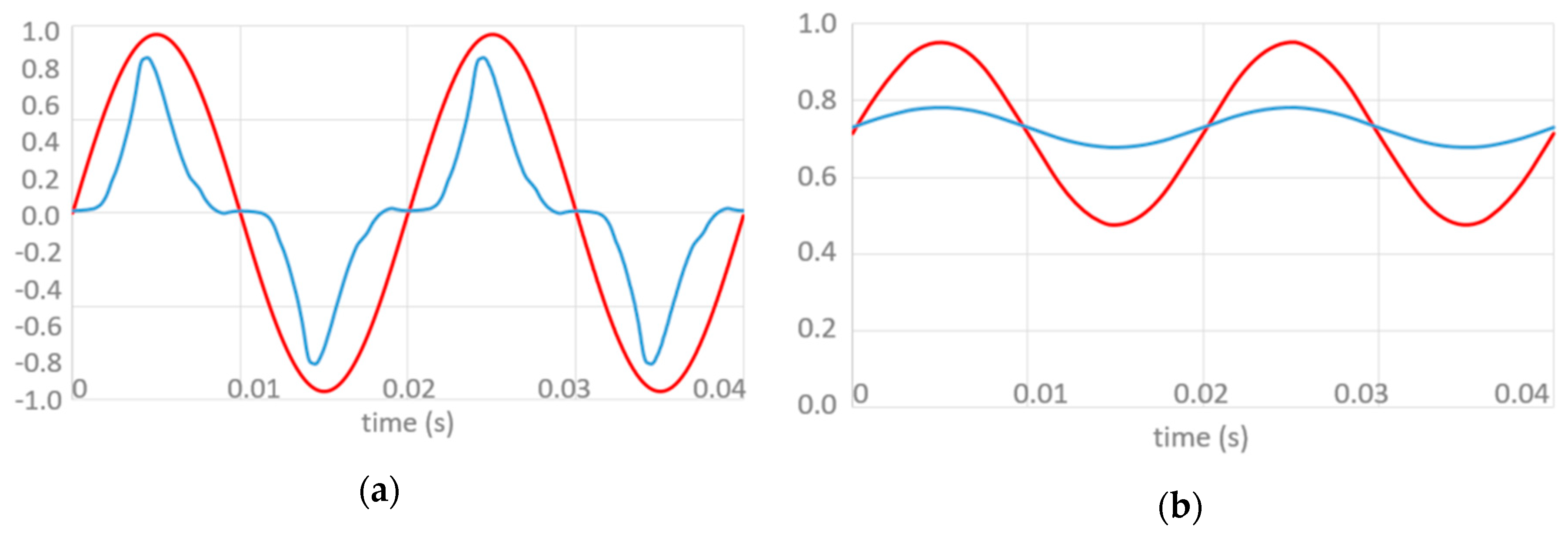
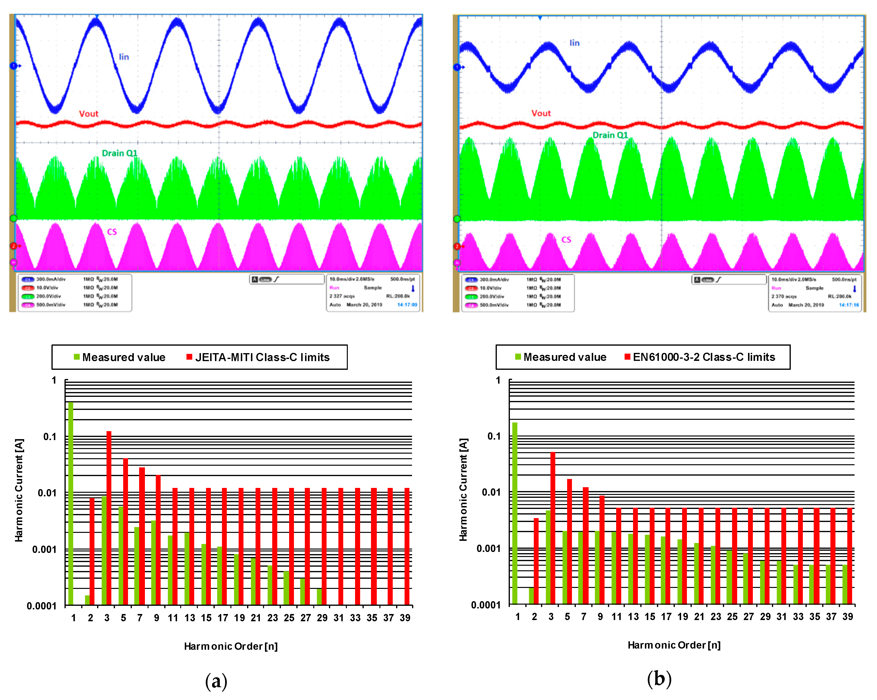
3.2. Experimental Verification of the Input Current Distortion in a Hi-PF QR Flyback LED Driver

A prototype of a Hi-PF QR flyback LED driver was set up to highlight the distortion occurring, even when a control method implementing the previous features is adopted. The main parameters of the converter are summarized in Table 1.
The prototype was built and its performance evaluated on the bench. The PF was greater than 0.98 over the input voltage range at full load. At 50% load, at low line it was nearly equal to that at 100% load, but at high line it dropped to about 0.97 at 230 Vac. Figure 11 depicts the experimental waveforms of the input current Iac(θ) (blue trace), the output voltage (red trace), the drain current of the MOSFET (green trace) and the current sense voltage reference for the controller (purple trace). The measurements were carried out at full load both at 110 Vac (60 Hz) and 230 Vac (50 Hz). From the experimental evidence, the shape of the measured Iac(θ) was very close to an ideal sinusoid waveform. It is worth noting that the harmonic contribution the prototype boards met the European norm EN61000-3-2 Class-C and Japanese norm JEITA_MITI Class-C, both of which are relevant to lighting equipment, at full load and nominal input voltage mains, as depicted in Figure 11.
A small distortion in the input current is apparent in Figure 11 (blue trace) by looking at the zero crossing of the waveform. Therefore, as previously mentioned, notwithstanding the enhanced performance of a Hi-PF QR flyback LED driver, there are still different inherent causes of distortion in the input current that are not ascribable to the specific control method. The causes are the ringing current, the crossover distortion due to transformer leakage inductance and crossover distortion due to the input storage capacitor. Generally speaking, being the converter in a nonlinear system, the overall THD of the input current cannot be the sum of each individual distortion contribution. Due to the number and the complexity of the distortion causes and, above all, due to the complexity of their mutual multi-interactions, the only way to have a sensible estimate of the overall result in terms of input current THD is to resort to simulations.
It is worth noting that the distortion of the input current Iac(θ) caused by the ringing effect has already been studied theoretically for boost PFC [55,56,57], while in the case of a Hi-PF QR flyback it has not yet been treated. Furthermore, the crossover distortion due to the input storage capacitor in the case of a Hi-PF flyback LED driver has never been studied. Finally, the crossover distortion due to transformer leakage inductance has also been theoretically analyzed in depth.

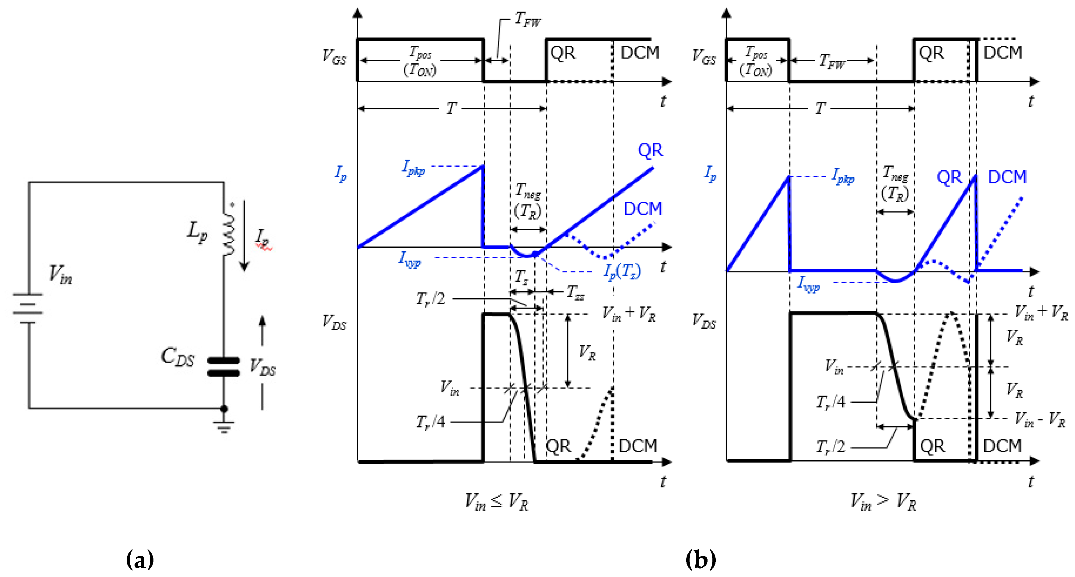
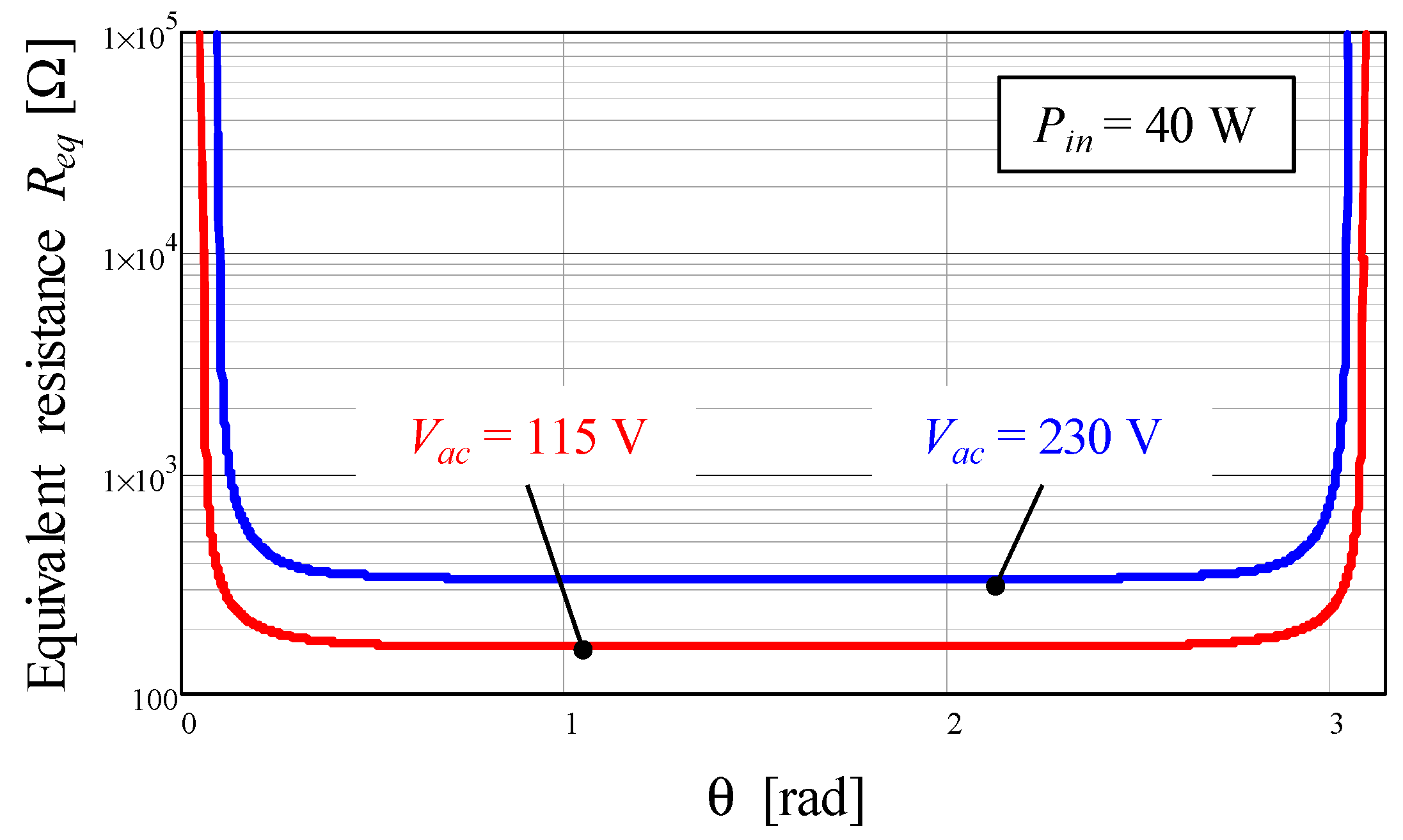
3.3. Distortion Caused by the Ringing Current

In a flyback, the drain-to-source voltage rings as soon as the secondary winding is fully demagnetized. The energy is exchanged between the total capacitance CDS of the drain node and the primary inductance of the flyback transformer Lp. For the sake of simplicity, assumption 3 has been assumed, and consequentially it has been carried out an equivalent circuit of the QR flyback during the time interval Tneg, which is the duration of the negative portion of the primary current, Ip. The duration of the positive portion, Tpos, of the primary current is equal to TON when the current in the turn-on instant of the power switch is zero. The simplified circuit model and the key waveforms are depicted in Figure 12.
In Figure 12a, the voltage across Lp is equal to the reflected output voltage VR, which is almost constant during TFW, according to the previous assumption 6. After that, the voltage across Lp and CDS and the current trough them start to oscillate. More specifically, the analytical expressions of VDS(t) and Ip(t) in the time interval Tneg, can be written as:
V D S ( t ) = { V i n ( t ) + V R cos ( 2 π t T r ) 0 < t T z 0 T z < t T n e g
I p ( t ) = { Y L V R sin ( 2 π t T r ) 0 < t T z I p ( T z ) + V i n L p t T z < t T n e g
Y L = C D S L p
where YL is the characteristic admittance of the CDS-Lp tank circuit and Tz is the time interval needed for the VDS to fall zero when Vin < VR; that is:
V R cos ( 2 π T z T r ) = V i n ( T z )
When QR-mode is adopted, the device can be turned on, but according to assumption 5, the current must reach zero. Tzz is the time interval needed for the primary current Ip to ramp linearly until zero from the current value Ip(Tz). In DCM operation, considering that Ip oscillates around zero, and that ringing is damped, after a few ringing cycles, assumption 7 can be considered exactly true; with QR operation, the negative current just after demagnetization is not compensated by subsequent positive contributions as in DCM. Considering zero the average value of Ip, as per assumption 7, is already a better approximation as compared to totally neglecting TR (i.e., assuming the operation is exactly at the boundary between DCM and CCM). However, in this context, assumption 7 is just a simplification, whose impact on the shape of the input current, quantitatively expressed by its THD, needs to be assessed. Being the ringing current at the turn-on instant of the power switch equal to the initial current during the on-time interval, this current may or may not be zero, which has an impact on the shape of the input current and, consequently, on its THD too.
When Vin > VR, in QR-mode, the turn on occurs at the first valley of the ringing in the drain voltage that follows the transformer demagnetization. Therefore, in this case, Tneg is equal to Tr/2.
By neglecting the input capacitor Cs from the QR flyback schematic in Figure 7, the following considerations are valid: during Ton a charge Qpos is provided from the input source and stored in the transformer; during TFW, the energy is mostly delivered to the output; finally, in Tneg, a negative charge Qneg is returned to the input source. The average input current during a switching cycle can therefore be expressed as:
I p = Q p o s Q n e g T
As shown in Figure 9, the positive charge Qpos is clearly given by:
Q p o s = 1 2 I p k p T o n
To evaluate the absolute value of the negative charge Qneg, it is necessary to consider Equations (8)–(10), that describe the VDS(t) and Ip(t) variations in the time interval Tneg (when QR operation is only considered) and distinguish two cases.
  • Vin > VR. In the time interval (0, Tneg) VDS(t) is always greater than zero and the current Ip(t) is sinusoidal; Tneg equals half the ringing period. The average value of Ip(t) during Tneg is 2/π times the negative peak value |Ivyp| = YLVR, therefore:
    Q n e g = T n e g 2 π Y L V R = T r π Y L V R = 2 V R C D S
  • VinVR. The current Ip(t) is sinusoidal in the subinterval (0, Tz). Tz can be expressed as:
    T z = T r 2 ( 1 1 π cos 1 ( V i n V R ) )
    and the current Ip(t) evaluated when t = Tz is:
    I p ( T z ) = Y L V R 1 ( V i n V R ) 2
As depicted in Figure 12b, in the time interval Tzz, Ip(t) ramps up linearly to zero. Hence, Tzz can be expressed as:
T z z = L p V i n | I p ( T z ) |
Since Tneg is the sum of Tz and Tzz, it can be written:
T n e g = T z + T z z = T r 2 [ 1 + V R V i n 1 ( V i n V R ) 2 cos 1 ( V i n V R ) ]
which is always greater than Tr/2, except when Vin = VR. Finally, Qneg is given by the sum of the two contributions, Qneg1 during the subinterval (0, Tz) and Qneg2 during the subinterval (Tz, Tneg). After some mathematical steps, Qneg can be evaluated as:
Q n e g = Q n e g 1 + Q n e g 2 = 0 T z Y L V R cos ( 2 π t T r ) d t + T z T n e g I p ( T z ) + V i n L p t d t = 1 2 C D S ( V i n + V R ) 2 V i n
Considering Equation (12), the overall input current Iin(θ) can be found by adding the contributions obtained in Equations (7) and (13), which also takes into account the ringing oscillations along each line half-cycle. Hence it can be written as:
I i n ( θ ) = { 1 2 I p k p ( θ ) T o n ( θ ) T ( θ ) 2 T ( θ ) V R C D S V i n > V R 1 2 I p k p ( θ ) T o n ( θ ) T ( θ ) 1 2 T ( θ ) ( V i n + V R ) 2 V i n C D S V i n V R
It is evident that the positive term in Equation (20) does not introduce any distortion, provided that the generic control method provides Ipkp(θ), as in Equation (6), and satisfies Equation (4). The contribution of the ringing current, related exclusively to the negative terms, takes into account the ringing contributions derived in Equations (14) and (19). They represent a twofold effect: they downwards offset the input current waveform, which produces crossover distortion and, considered that the offset is a function of the instantaneous line voltage, they distort its shape as well. It is worth noting that the distortion contribution is not ascribable to the control method; that is, it is not due to the control but is inherent in the power processing mechanism of any Hi-PF QR flyback converter. On the other hand, the control method may compensate or mitigate it. First of all, the contribution of the ringing current can be reduced by lowering the switching frequency (i.e., a longer T(θ), obtained with a larger Lp value) and using a low reflected voltage VR. However, a larger Lp value implies a bigger flyback transformer, and a lower VR increases the primary rms current and, consequently, the conduction losses. A trade-off is therefore required. A smaller CDS also helps to reduce the ringing contribution, however, it is important to underline that a tradeoff between switching losses and EMI should be found. In fact, the lower the CDS, the faster the VDS transient at turn-off, and this faster transient may adversely affect both the efficiency of the power switch, as well as the EMI.
LED driver applications are typically specified to accommodate a certain range of output voltages Vout to power different types and lengths of LED string. Thus the contribution of the ringing current is expected to be maximum at the upper end of the Vout range and minimum at the lower end of the Vout range. In fact, lowering Vout will simultaneously reduce VR and increase T(θ).

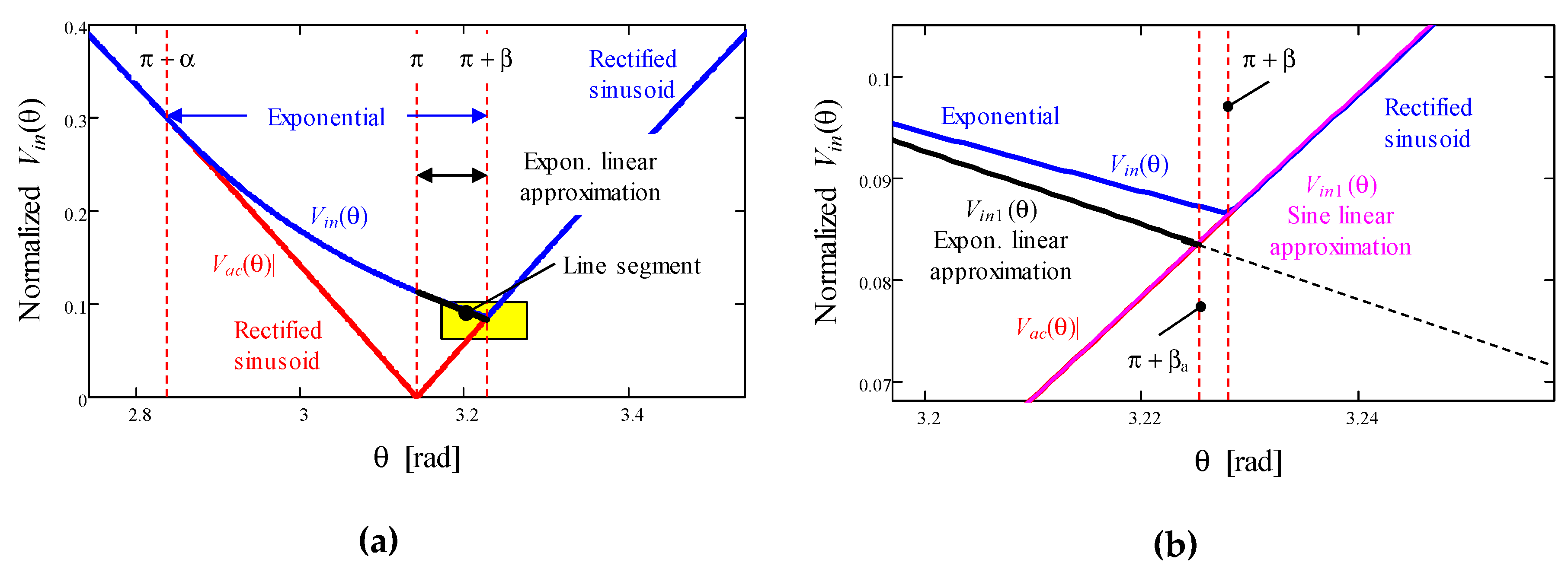
3.4. Crossover Distortion Due to the Input Capacitor

The storage capacitor Cs placed downstream of the input bridge, as depicted in Figure 7, is part of the EMI filter, which is always needed in an SMPS connected to the power line to restrict the conducted emission within the limits envisaged by the relevant EMI regulations. The capacitor has a twofold effect: it contributes to the voltage–current phase-shift and worsens the THD by maintaining a residual voltage on the dc side of the input bridge rectifier. The latter causes a non-conduction zone as the line voltage approaches zero, therefore, assumption 2 is no longer valid for the following analysis. This phenomenon also occurs for systems without a PFC and is an additional source of crossover itself, which interacts with the other distortion mechanisms. A quantitative analysis of this crossover distortion can be carried out independently from the topology employed in a PFC.
In these terms, any PFC and, consequently, the Hi-PF QR flyback converter can be modeled with an equivalent resistor (Req) that can be expressed as:
R e q = V P K 2 2 P i n
where VPK is the peak of the rectified line voltage Vin(θ) and Pin is the input power of the converter.
Generally speaking, the dead zone in Iac(θ) increases at large CS values, high line voltage and low load (large Req). In quantitative terms, the dead zone starts, near the zero-crossing, when the rate of fall in the line voltage Vac(θ) exceeds the rate of the voltage Vin (θ) across CS, limited by the time constant Req CS, so that from that instant on it is Vac(θ) < Vin(θ), as shown in Figure 13.
Focusing on the Vac(θ) and Vin(θ) near the zero-crossing zone, shown in Figure 13a, and neglecting the voltage drop across the input bridge rectifier, the phase angle α at which the slope of the two voltages are equal can be found with the following relation:
| d v a c ( θ ) d θ | = | d v i n ( θ ) d θ | 2 π f L V P K cos α = 1 R e q C s V P K sin α
Solving for α:
tan α = 2 π f L R e q C s
From π-α on, Vin(θ) follows an exponential decay until the phase θ is equal to π + β, where it is again |Vac(θ)| ≥ Vin(θ), which marks the end of the dead zone. In this interval the expression of Vin(θ) can be assumed as:
V i n ( θ ) = sin α e θ ( π α ) tan α
Beyond the angle π + β, Vac(θ) and Vin(θ) are again both sinusoidal and overlapping until they have a phase shift equal to α away from the next zero-crossing. The duration of the dead zone is clearly α + β.
The phase angle β can be found at the intersection of an exponential curve with a sinusoidal one, which results in a transcendental equation with no closed-form solution. Since β is small, it is possible to find an approximate solution βa, substituting the last part of the exponential function (from θ = π to θ = π + β) with its expansion in Taylor series to the first order (eθ 1−θ). In a similar way it can be done for the rectified sinusoid (sin θ ≈ θ). Therefore, the value Λ of the input voltage, evaluated when the phase angle is π, can be computed as follows:
Λ = V i n ( π ) = sin α e α tan α sin α e
As shown in Figure 13b, at the intersection of the two straight lines, the phase angle is π + βa.
{ V i n 1 ( θ ) = Λ ( 1 θ π tan α ) V i n 2 ( θ ) = θ π β a = Λ tan α Λ + tan α
The truncation of the exponential Equation (24) to the first order introduces an underestimation, as depicted in Figure 13b, hence Equation (26) provides an approximated value βa < β. On the other hand, if Equation (24) is approximated to the second order, which provides a better approximation of Equation (24), an overestimation will result and the approximated value βa > β is less than 4% larger than the value provided by Equation (26), which proves that the accuracy of the first assumption is valid anyway.
The previous analysis shows that the storage capacitor CS can be assumed as a source of crossover distortion, even if Req is a real resistor. The key point is the inability of Vin(θ) to keep pace with Vac(θ) on the falling edge of the sinusoid, due to the maximum discharge rate of CS through Req. However, its net impact is the result of the interaction with the other sources of distortion, previously analyzed.
In fact, it has been assumed that a resistor Req that represents the whole converter, which implicitly means that the ratio of Vin (θ) to Iin(θ) is constant in (0, π); i.e., Iin(θ) is pure sinusoidal in (0, π). Actually, the distortion of the current shape, caused by all the previously considered sources, tends to reduce Iin(θ) with respect to the undistorted case. Instead, considering the same model approach, if it can be assumed that the Req changes along the sinusoid, then Req = Req(θ) = Vin(θ)/Iin(θ). Figure 14 shows Req(θ) obtained by dividing a sinusoidal input voltage and the current drawn that takes into account the distortion caused by the ringing current in Equation (20).
Req(θ) is almost flat for a wide range of the sinusoid except when the current is approaching the zero crossings. The increase in Req(θ) produces an early dead zone with respect to the case with a fixed Req. The corresponding value of α would be the solution of the equation:
tan α = 2 π f L R e q ( α ) C s
The solution of Equation (27) must be defined in the interval (π/2, π), where tan α has a finite value and consequentially also Req(α). As a result, the dead zone caused by the input capacitor Cs starts before Req(θ) diverges, and Iac(θ) must cross zero before Iin(θ). In other words, as long as the bridge rectifier conducts, Iac(θ) is the sum of Iin(θ) and the current through CS, which is essentially a sinusoid leading by 90 degrees. This causes Iac(θ) to lead Iin(θ), whereas without CS they would be essentially coincident.
Within the dead zone, the relation Req(θ) = Vin(θ)/Iin(θ) is no longer the one shown in the diagram of Figure 14 because of both the voltage Vin(θ) and the Iin(θ) are not sinusoidal. Besides, the voltage retained by Cs, which makes Vin(θ) > |Vac(θ)|, and TON(θ) and T(θ) will be much smaller than those predicted during the control method design, which was carried out assuming a sinusoidal input voltage, as per Equation (5). The resulting switching frequency may be higher. As long as some energy is delivered to the output, CS (which is the only source of energy, since no current comes from the reverse-biased bridge rectifier), keeps on discharging and as long as Iin(θ) > 0. If the peak current becomes lower than the critical peak primary current for no energy transfer, the energy is no longer transferred to the output and bounces back and forth between CS and Lp, except for the energy dissipated during this process. As a consequence, CS is discharged at a lower rate. Instead, if the peak current does not go below that critical value, the discharge rate of CS has no change.
When |Vac(θ)| ≥ Vin(θ) and the dead zone ends at θ = β, it is possible to observe an abrupt variation in Iac(θ). This is caused by the bridge rectifier that is forward-biased, as Iac(θ) has to transition from zero to Iac(β), which is already greater than zero because of the leading phase of Iac(θ).
It is worth mentioning that, near the zero crossing interval, the input voltage is far from constant in a switching cycle and the switching frequency may come close to the frequency related to the resonance between CS and Lp. So, the Vin(θ) has sinusoidal behavior, rather than constant. Additionally, the resonance of the inductors and capacitors in the EMI filter can also be stimulated, so that different resonance phenomena may coexist. This means that the modeling approach used throughout the present discussion is not always valid in describing the practical behavior.

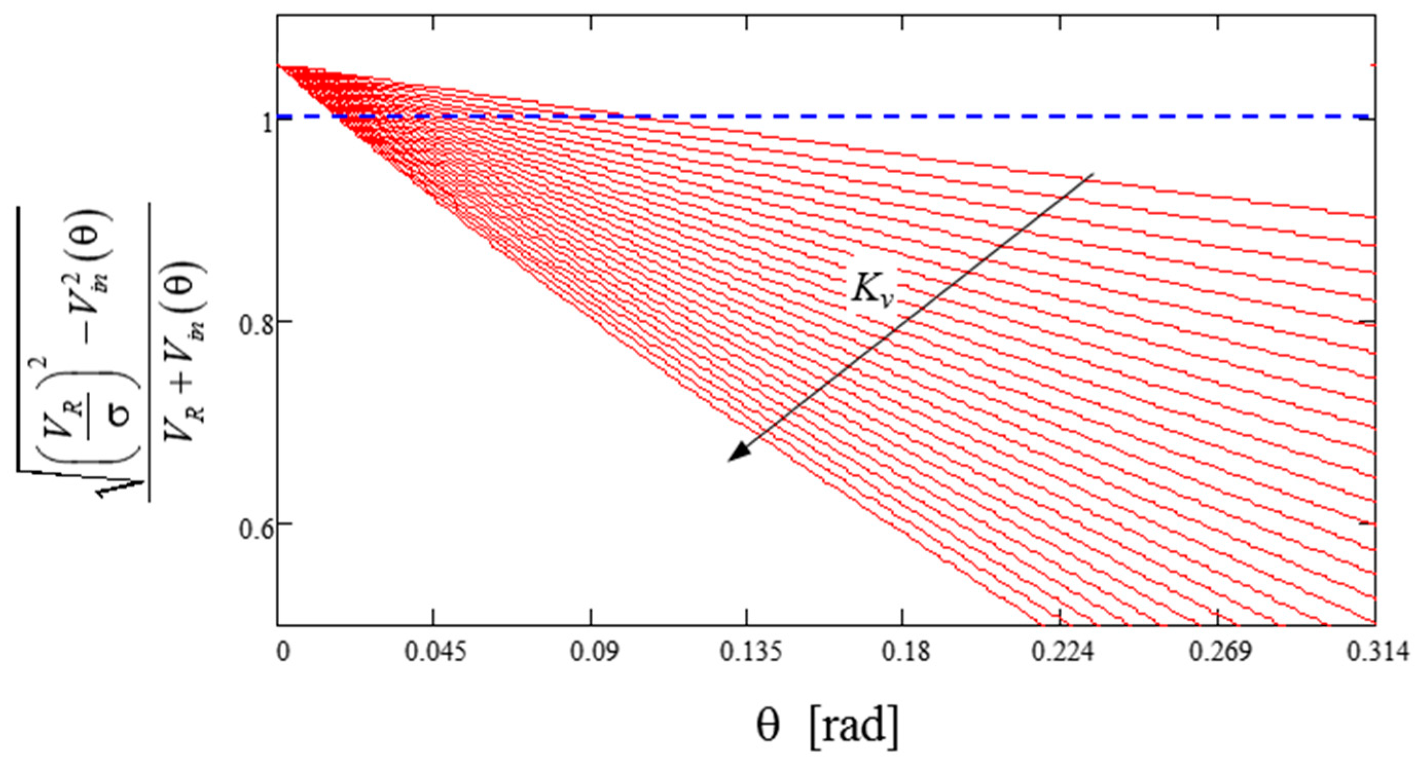
3.5. Crossover Distortion Due to Transformer’s Leakage Inductance

In practical cases, the real transformer’s windings are not perfectly coupled. This phenomenon causes a crossover distortion that affects the input current shape and degrades the THD. Therefore, in the following subsection, the analysis of the distortion no longer takes into account assumptions 3 and 4.
In a real transformer, a portion of the energy stored in the primary winding cannot be transferred to the secondary winding because of imperfect magnetic coupling. In other words, this can be modeled by considering the primary inductance Lp split into two distinct elements: the magnetizing inductance LM perfectly coupled to the secondary winding and the leakage inductance Llk (uncoupled). In these terms, it is useful to define the coupling coefficient σ such that LM = σ Lp and Llk = (1− σ) Lp. Typical values of σ range from 0.95 to 0.99.
The energy stored in the leakage inductance is not transferred to the output and this energy would overcharge CDS well over Vin(θ) + VR, in most cases exceeding the voltage rating of the power switch. A typical solution is to use a clamp circuit which limits VDS(t) at a well-defined and properly selected value VCL (> VR) above Vin(θ). Figure 15 shows the equivalent circuit of the Hi-PF QR flyback converter during the off time and the current waveforms underlining the effect of Llk.
When the power switch is turned off, the primary current firstly charges the capacitance CDS, thus the VDS(t) evolves until the voltage of the magnetizing inductance LM, VM, equals –VR. During this time interval Tps, the primary current Ip is flowing through LM and Llk, so there is an inductive voltage divider. Therefore:
V M = L M L p V p = L M L p [ V i n ( θ ) V D S ( t ) ]
In the instant when the voltage VM equals –VR, the voltage Vp across the primary winding can be expressed as:
V p = L p L M V R = 1 σ V R
Immediately after the time interval Tps, the current starts flowing through D1 and the energy starts being transferred to the output. VDS(t) keeps on ramping up until it reaches Vin (θ) + VCL in a time TLK. After that, VDS(t) is clamped, Llk starts being demagnetized with a rate equal to (VRVCL)/Llk and the current through D1 reduces at the same rate. The portion of the primary current Ip(t) of the leakage inductance varies from the peak value, Ipkp(θ), until zero in a time interval equal to TLK(θ). Hence:
I p ( t ) = I p k p ( θ ) V C L V R ( 1 σ ) L p t
As soon as Ip(t) is equal to zero, it can be written in the analytical expression of TLK:
T L K ( θ ) = ( 1 σ ) L p V C L V R I p k p ( θ )
Bearing in mind the current that flows in LM can be written as:
I M ( t ) = I p k p ( θ ) V R σ L p t
Meanwhile, the secondary current reaches its peak value Ipks(θ):
I p k s ( θ ) = n I M ( T L K ) = n [ 1 V R V C L V R 1 σ σ ] I p k p ( θ )
After that, the magnetizing inductance on the secondary side starts being demagnetized at a rate VR/LM until it zeroes in a time TDEM, as shown in Figure 15. The presence of Llk splits the time interval TFW in a first subinterval TLK needed to demagnetize the leakage inductance (and magnetize the secondary winding) and a second subinterval TDEM needed to demagnetize the secondary winding. It is possible to prove that the resulting TFW can be expressed as:
T F W ( θ ) = L M V R I p k p ( θ ) = σ L p V R I p k p ( θ )
(i.e., the one calculated neglecting the leakage inductance multiplied by the coupling coefficient σ).
The presence of Llk clearly compromises the input-to-output transfer energy, thus the dead zone where there is no energy transfer is expected to occur over a wider phase angle range of the line voltage. In fact, the “no energy transfer” condition concerns only the portion of the primary voltage Vp across the magnetizing inductance LM. Combining Equations (8), (9) and (28), it is possible to find that the condition for no energy transfer, solved for Ipkp(θ), yields:
I p k p ( θ ) Y L ( V R σ ) 2 V i n 2 ( θ )
The critical peak primary current for no energy transfer, expressed by Equation (35), is larger than the ideal case (σ = 1), thus confirming the forecast of a wider dead zone related to this phenomenon.
It is noteworthy to compare the critical value of Ipkp(θ) in Equation (35) to that determined by the ringing current after demagnetization and the relative positions of the dead zones they generate.
Bearing in mind that the on time can be written as:
T O N = L p V i n I p k p
The region around zero crossings where there is no input-to-output energy transfer (Iin(θ) = 0), can be written by considering the combination of the input current in Equation (20) in the case of Vin < VR, and Equation (36):
I p k p = ( V i n + V R ) 2 V i n C D S L p V i n I p k p
Combining Equations (10)–(37), the ringing current after demagnetization related to the dead zone can be expressed as:
I p k p ( θ ) Y L [ V i n ( θ ) + V R ]
Figure 16 shows the ratio of the critical value of Ipkp(θ) for no input-to-output energy transfer, as in Equation (35), to that caused by the ringing current, as in Equation (38). The ratio is expressed as a function of the parameter Kv:
K v = V P K V R
where VPK is the peak value of the rectified line voltage Vin(θ). The dashed blue line represents the ideal case. As is evident from Figure 16, the dead zone becomes even larger near the zero crossings. Therefore, the lack of input-to-output energy transfer may override the dead zone caused by the ringing current needed for the demagnetization of the secondary winding in a time TDEM.

4. Conclusions

The standard limitations regarding the input current distortion in LED driver applications may be stringent, especially in large lighting systems. Therefore, the choice of a proper LED driver aiming at current harmonics reduction is crucial. At the same time, the solution must be economical, compact and reliable.
The QR flyback shows the highest figure of merit (FOM) among the different LED driver solutions analyzed in the literature. With this aim, this work has investigated and has analyzed the different inherent causes of distortion in the input current and the power processing mechanism of the proposed QR flyback converter that are not ascribable to the control method.
Several effects, such as the distortion caused by the ringing current, crossover distortion due to transformer leakage inductance and crossover distortion due to the input storage capacitor, have been analyzed in depth. It is important to point out that the converter is a nonlinear system and, consequentially, the overall THD of the input current cannot be evaluated as a simple sum of the THD associated to each individual contribution, where the aforementioned issues are mutually interacting or partly overlapping, such as those creating a dead zone in the line current.
Some useful design hints have been extracted and discussed in order to provide some suggestions for an optimized design of a QR flyback LED driver converter. In detail, the following list summarizes all the possible precautions to bear in mind.
  • The impact of the ringing current after transformer demagnetization can be mitigated by lowering the switching frequency, using a low reflected voltage VR or choosing a power MOSFET with a RDS(on) with an optimized RDS(on)/Coss FOM. These criteria also help to reduce the phenomenon of the lack of input-to-output energy transfer near the zero crossings of the line voltage.
  • The leakage inductance of the transformer should be kept as low as practically possible. This choice essentially optimizes the converter efficiency but does not impact the reduction in the dead zones near the zero crossings of the line voltage caused by other phenomena (essentially, the input capacitor CS).
  • The input storage capacitor CS should be minimized to reduce the dead zone near the line voltage zero crossings and the current leap occurring in the proximity of the dead zone. However, particular attention should be paid to the following points.
    • The diodes of the input bridge rectifier are usually slow-recovery ones, so the primary current at the switching frequency may require an enhanced filter on the ac side of the bridge and may cause the diodes of the bridge to overheat.
    • Close to the zero crossings, the switching frequency can be very low. If the ringing frequency related to CS and Lp is comparable with the switching one, it may generate current spikes that would degrade the current THD.
  • Class-X capacitors are generally used along with inductors for EMI filtering, necessary for the certification of the final product. Class-X capacitors can degrade the PF, although they do not contribute to the THD. From this perspective, on the one hand, the design of the filter must make the device compliant with the standards. On the other hand, there is a degree of freedom that can be exploited to minimize PF lowering at high line and light load. The filters should be designed with the largest inductance and the smallest capacitance practically possible.

Author Contributions

All authors contributed equally to this work. Writing-Review & Editing, C.A.; Writing-Review & Editing, G.G.; Writing-Review & Editing, A.R.; Writing-Review & Editing, S.A.R.; Writing-Review & Editing, G.S. All authors have read and agreed to the published version of the manuscript.

Funding

This research received no external funding.

Conflicts of Interest

The authors declare no conflict of interest.

Nomenclature

V a c ( t , θ ) [V]Line voltage input.
V i n ( t , θ ) [V]Rectified line voltage.
V P K [V]Peak of the rectified line voltage Vin (θ).
I a c ( t , θ ) [A]Line input current.
I p ( t ,   θ ) [A]Current on the primary windings.
I s ( t , θ ) [A]Current on the secondary windings.
I o u t [A]Output constant current.
V o u t [V]Output constant voltage.
L P [Ω]Inductance of the primary windings.
L s [Ω]Inductance of the secondary windings.
T o n [s]On time of the power switch
T F W [s]Time interval where the current flows on the secondary side.
T n e g [s]Time interval where the drain–source voltage rings
T [s]Time interval of the switching period.
C D S [F]Drain to source capacitance of the MOSFET.
V D S ( t ) [V]Drain to source voltage of the MOSFET.
I p k p ( θ ) [A]Current amplitude on the primary windings.
V R [V]Reflected voltage.
T r [s]Time period of drain voltage ringing.
T z [s]Time interval needed for VDS to fall to zero.
T z z [s]Time interval needed for primary current to ramp linearly until zero.
Y L [Ω]Characteristic admittance of the CDS-Lp tank circuit.
Q p o s [C]Charge accumulates from the input source.
Q n e g [C]Charge returned to the input source.
L M [Ω]Magnetizing inductance.
T L K [s]Time interval needed to demagnetize the leakage inductance.
σ Coupling coefficient of Lm.
I p k s ( θ ) [A]Current amplitude on the secondary windings.
R e q [Ω]Equivalent resistor of the converter.
P i n [W]Input power.

References

  1. Shabbir, H.; Ur Rehman, M.; Rehman, S.A.; Sheikh, S.K.; Zaffar, N. Assessment of harmonic pollution by LED lamps in power systems. In Proceedings of the Clemson University Power Systems Conference, Clemson, SC, USA, 11–14 March 2014; pp. 1–7. [Google Scholar]
  2. Mehta, R.; Deshpande, D.; Kulkarni, K.; Sharma, S.; Divan, D. A Competitive Solution for General Lighting Applications. In Proceedings of the IEEE Energy 2030 Conference, Atlanta, GA, USA, 17–18 November 2008; pp. 1–5. [Google Scholar]
  3. Moriarty, P.; Honnery, D. Energy policy and economics under climate change. AIMS Energy 2018, 6, 272–290. [Google Scholar] [CrossRef]
  4. Hsu, Y.-C.; Lin, J.-Y.; Chen, C.C.-P. Area-Saving and High-Efficiency RGB LED Driver with Adaptive Driving Voltage and Energy-Saving Technique. Energies 2018, 11, 1422. [Google Scholar] [CrossRef] [Green Version]
  5. Ramljak, I.; Amir Tokić, A. Harmonic emission of LED lighting. AIMS Energy 2020, 8, 1–26. [Google Scholar] [CrossRef]
  6. Nagaraj, C.; Manjunatha Sharma, k. Fuzzy PI controller for bidirectional power flow applications with harmonic current mitigation under unbalanced scenario. AIMS Energy 2018, 6, 695–709. [Google Scholar]
  7. Lee, E.S.; Nguyen, D.T.; Rim, C.T. A novel passive type LED driver for static LED power regulation by multi-stage switching circuits. In Proceedings of the IEEE Applied Power Electronics Conference and Exposition (APEC), Charlotte, NC, USA, 15–19 March 2015; pp. 900–905. [Google Scholar]
  8. Wang, Y.; Huang, J.; Shi, G.; Wang, W.; Xu, D. A Single-Stage Single-Switch LED Driver Based on the Integrated SEPIC Circuit and Class-E Converter. IEEE Trans. Power Electron. 2016, 31, 5814–5824. [Google Scholar] [CrossRef]
  9. Hu, Y.; Huber, L.; Jovanovic, M. Single-Stage Flyback Power-Factor-Correction Front-End for HB LED Application. In Proceedings of the IEEE Industry Applications Society Annual Meeting, Houston, TX, USA, 4–8 October 2009; pp. 1–8. [Google Scholar]
  10. Maksimovic, D.; Cuk, S. Switching converters with wide DC conversion range. IEEE Trans. Power Electron. 1991, 6, 151–157. [Google Scholar] [CrossRef]
  11. Huber, L.; Jovanovic, M. Single-stage single-switch input-current-shaping technique with reduced switching loss. IEEE Trans. Power Electron. 2000, 15, 681–687. [Google Scholar] [CrossRef]
  12. Chiu, H.J.; Cheng, S.J. LED backlight driving system for large-scale LCD panels. IEEE Trans. Ind. Electron. 2007, 54, 2751–2760. [Google Scholar] [CrossRef]
  13. Nassary, M.; Orabi, M.; Arias, M.; Ahmed, E.M.; Hasaneen, E.-S. Analysis and Control of Electrolytic Capacitor-Less LED Driver Based on Harmonic Injection Technique. Energies 2018, 11, 3030. [Google Scholar] [CrossRef] [Green Version]
  14. Chiu, H.J.; Song, T.H.; Cheng, S.J.; Li, C.H.; Lo, Y.K. Design and implementation of a single-stage high-frequency HID lamp electronic ballast. IEEE Trans. Ind. Electron. 2008, 55, 674–683. [Google Scholar] [CrossRef]
  15. Li, Y. A Novel Control Scheme of Quasi-Resonant Valley-Switching for High-Power-Factor AC-to-DC LED Drivers. IEEE Trans. Ind. Electron. 2015, 62, 4787–4794. [Google Scholar] [CrossRef]
  16. IEEE-1459-2010 Standard—IEEE Standard Definitions for the Measurements of Electric Power Quantities under Sinusoidal, Nonsinusoidal, Balanced or Unbalanced Conditions; IEEE: New York, NY, USA, 2010.
  17. Chen, W.; Li, S.N.; Hui, S.Y.R. A comparative study on the circuit topologies for offline passive light-emitting diode (LED) drivers with long lifetime & high efficiency. In Proceedings of the 2010 IEEE Energy Conversion Congress and Exposition (ECCE), Atlanta, GA, USA, 12–16 September 2010; pp. 724–730. [Google Scholar]
  18. Lee, B.; Kim, H.; Rim, C. Robust Passive LED Driver Compatible with Conventional Rapid-Start Ballast. IEEE Trans. Power Electron. 2011, 26, 3694–3706. [Google Scholar] [CrossRef]
  19. Hui, S.Y.; Li, S.N.; Tao, X.H.; Chen, W.; Ng, W.M. A Novel Passive Offline LED Driver with Long Lifetime. IEEE Trans. Power Electron. 2010, 25, 2665–2672. [Google Scholar] [CrossRef]
  20. Wang, Y.; Alonso, J.M.; Ruan, X. A Review of LED Drivers and Related Technologies. IEEE Trans. Ind. Electron. 2017, 64, 5754–5765. [Google Scholar] [CrossRef]
  21. Yada, T.; Katamoto, Y.; Yamada, H.; Tanaka, T.; Okamoto, M.; Hanamoto, T. Design and Experimental Verification of 400-W Class LED Driver with Cooperative Control Method for Two-Parallel Connected DC/DC Converters. Energies 2018, 11, 2237. [Google Scholar] [CrossRef] [Green Version]
  22. Pinto, R.A.; Cosetin, M.R.; Marchesan, T.B.; Cervi, M.; Campos, A.; Do Prado, R.N. Compact lamp using high-brightness LEDs. In Proceedings of the IEEE Industry Applications Society Annual Meeting, Edmonton, AB, Canada, 5–9 October 2008; pp. 1–5. [Google Scholar]
  23. Li, Y.Y.-C.; Chen, C.-L.C. A novel single-stage high-power-factor AC-to-DC LED driving circuit with leakage inductance energy recycling. IEEE Trans. Ind. Electron. 2012, 59, 793–802. [Google Scholar] [CrossRef]
  24. Alonso, J.M.; Vina, J.; Vaquero, D.G.; Martinez, G.; Osorio, R. Analysis and design of the integrated double buck–boost converter as a high-power-factor driver for power-LED lamps. IEEE Trans. Ind. Electron. 2012, 59, 1689–1697. [Google Scholar] [CrossRef]
  25. Qu, X.; Wong, S.C.; Tse, C.K. Resonance-assisted buck converter for offline driving of power LED replacement lamps. IEEE Trans. Power Electron. 2011, 26, 532–540. [Google Scholar]
  26. Qin, Y.; Chung, H.; Lin, D.Y.; Hui, S.Y.R. Current source ballast for high power lighting emitting diodes without electrolytic capacitor. In Proceedings of the 34th Annual Conference of IEEE Industrial Electronics, Orlando, FL, USA, 10–13 November 2008; pp. 1968–1973. [Google Scholar]
  27. Hwu, K.-I.; Tai, Y.-K.; He, Y.-P. Bridgeless Buck-Boost PFC Rectifier with Positive Output Voltage. Appl. Sci. 2019, 9, 3483. [Google Scholar] [CrossRef] [Green Version]
  28. Ma, H.; Lai, J.; Feng, Q.; Yu, W.; Zheng, C.; Zhao, Z. A Novel Valley-Fill SEPIC-Derived Power Supply without Electrolytic Capacitor for LED Lighting Application. IEEE Trans. Power Electron. 2012, 27, 3057–3071. [Google Scholar] [CrossRef]
  29. Hariprasath, S.; Balamurugan, R. A valley-fill SEPIC-derived power factor correction topology for LED lighting applications using one cycle control technique. In Proceedings of the International Conference on Computer Communication and Informatics, Coimbatore, India, 4–6 January 2013; pp. 1–4. [Google Scholar]
  30. Wu, X.; Wang, Z.; Zhang, J. Design Considerations for Dual-Output Quasi-Resonant Flyback LED Driver with Current-Sharing Transformer. IEEE Trans. Power Electron. 2013, 28, 4820–4830. [Google Scholar] [CrossRef]
  31. Shagerdmootaab, A.; Moallem, M. Filter Capacitor Minimization in a Flyback LED Driver Considering Input Current Harmonics and Light Flicker Characteristics. IEEE Trans. Power Electron. 2015, 30, 4467–4476. [Google Scholar] [CrossRef]
  32. Arias, M.; Lamar, D.G.; Linera, F.F.; Balocco, D.; Aguissa Diallo, A.; Sebastián, J. Design of a Soft-Switching Asymmetrical Half-Bridge Converter as Second Stage of an LED Driver for Street Lighting Application. IEEE Trans. Power Electron. 2012, 27, 1608–1621. [Google Scholar] [CrossRef]
  33. Kim, C.; Kim, E.; Shin, H. A study on the power LEDs drive circuit design with asymmetrical half-bridge resonant converter. In Proceedings of the International Conference on Electrical Machines and Systems, Tokyo, Japan, 15–18 November 2009; pp. 1–4. [Google Scholar]
  34. Arias, M.; Diaz, M.F.; Cadierno, J.E.R.; Lamar, D.G.; Sebastián, J. Digital Implementation of the Feedforward Loop of the Asymmetrical Half-Bridge Converter for LED Lighting Applications. IEEE J. Emerg. Sel. Top. Power Electron. 2015, 3, 642–653. [Google Scholar] [CrossRef] [Green Version]
  35. Castro, I.; Martin, K.; Vazquez, A.; Arias, M.; Lamar, D.G.; Sebastian, J. An AC–DC PFC Single-Stage Dual Inductor Current-Fed Push–Pull for HB-LED Lighting Applications. IEEE J. Emerg. Sel. Top. Power Electron. 2018, 6, 255–266. [Google Scholar] [CrossRef] [Green Version]
  36. Mohamadi, A.; Afjei, E. A single-stage high power factor LED driver in continuous conduction mode. In Proceedings of the 6th Power Electronics, Drive Systems & Technologies Conference (PEDSTC2015), Tehran, Iran, 3–4 February 2015; pp. 462–467. [Google Scholar]
  37. Wang, L.; Zhang, B.; Qiu, D. A Novel Valley-Fill Single-Stage Boost-Forward Converter with Optimized Performance in Universal-Line Range for Dimmable LED Lighting. IEEE Trans. Ind. Electron. 2017, 64, 2770–2778. [Google Scholar] [CrossRef]
  38. Chen, S.-M.; Liang, T.-J.; Yang, L.-S.; Chen, J.-F. A safety enhanced, high step-up DC-DC converter for AC photovoltaic module application. IEEE Trans. Power Electron. 2012, 27, 1809–1817. [Google Scholar] [CrossRef]
  39. Cheng, C.; Chang, C.; Cheng, H.; Tseng, C. A novel single-stage LED driver with coupled inductors and interleaved PFC. In Proceedings of the 9th International Conference on Power Electronics and ECCE Asia (ICPE-ECCE Asia), Seoul, Korea, 1–5 June 2015; pp. 1240–1245. [Google Scholar]
  40. Cheng, C.; Cheng, H.; Chung, T. A novel single-stage high-power-factor LED street-lighting driver with coupled inductors. In Proceedings of the IEEE Industry Applications Society Annual Meeting, Lake Buena Vista, FL, USA, 6–11 October 2013; pp. 1–7. [Google Scholar]
  41. Duan, R.-Y.; Lee, J.-D. High-efficiency bidirectional DC-DC converter with coupled inductor. IET Power Electron. 2012, 5, 115–123. [Google Scholar] [CrossRef]
  42. Vecchia, M.D.; Van den Broeck, G.; Ravyts, S.; Tant, J.; Driesen, J. Modified step-down series-capacitor buck converter with insertion of a Valley-Fill structure. IET Power Electron. 2019, 12, 3306–3314. [Google Scholar] [CrossRef]
  43. Xu, S.; Shen, W.; Qian, Q.; Zhu, J.; Sun, W.; Li, H. An efficiency optimization method for a high frequency quasi-ZVS controlled resonant flyback converter. In Proceedings of the IEEE Applied Power Electronics Conference and Exposition (APEC), Anaheim, CA, USA, 17–21 March 2019; pp. 2957–2961. [Google Scholar]
  44. Tabisz, W.A.; Gradzki, P.M.; Lee, F.C.Y. Zero-voltage-switched quasi-resonant buck and flyback converters-experimental results at 10 MHz. IEEE Trans. Power Electron. 1989, 4, 194–204. [Google Scholar] [CrossRef]
  45. Gritti, G.; Adragna, C. Analysis, design and performance evaluation of an LED driver with unity power factor and constant-current primary sensing regulation. AIMS Energy 2019, 7, 579–599. [Google Scholar] [CrossRef]
  46. Zhang, S.; Liu, X.; Guan, Y.; Yao, Y.; Alonso, J.M. Modified zero-voltage-switching single-stage LED driver based on Class E converter with constant frequency control method. IET Power Electron. 2018, 11, 2010. [Google Scholar] [CrossRef]
  47. Jeng, L.S.; Peng, T.M.; Hsu, Y.C.; Chieng, H.W.; Shu, J.P. Quasi-Resonant Flyback DC/DC Converter Using GaN Power Transistors. World Electr. Veh. J. 2012, 5, 567–573. [Google Scholar] [CrossRef] [Green Version]
  48. Xie, X.; Li, J.; Peng, K.; Zhao, C.; Lu, Q. Study on the Single-Stage Forward-Flyback PFC Converter With QR Control. IEEE Trans. Power Electron. 2016, 31, 430–442. [Google Scholar] [CrossRef]
  49. Wang, Z.; Wu, X.; Chen, M.; Zhang, J. Optimal design methodology for the current-sharing transformer in a quasi-resonant (QR) flyback LED driver. In Proceedings of the Twenty-Seventh Annual IEEE Applied Power Electronics Conference and Exposition (APEC), Orlando, FL, USA, 5–9 February 2012; pp. 2372–2378. [Google Scholar]
  50. Li, J.; Liang, T.; Chen, K.; Lu, Y.; Li, J. Primary-side controller IC design for quasi-resonant flyback LED driver. In Proceedings of the IEEE Energy Conversion Congress and Exposition (ECCE), Montreal, QC, Canada, 20–24 September 2015; pp. 5308–5315. [Google Scholar]
  51. Zhang, J.; Zeng, H.L.; Wu, X.K. An Adaptive Blanking Time Control Scheme for an Audible Noise-Free Quasi-Resonant Flyback Converter. IEEE Trans. Power Electron. 2011, 26, 2735–2742. [Google Scholar] [CrossRef]
  52. Chen, K.; Chiu, C.C.; Lin, M.; Yeh, C.P.; Lin, J.M.; Chen, K.H. Quasi-Resonant Control with Dynamic Frequency Selector and Constant Current Startup Technique for 92% Peak Efficiency and 85% Light-load Efficiency Flyback Converter. IEEE Trans. Power Electron. 2013, 29, 4959–4969. [Google Scholar]
  53. Ringel, M.; Schlomann, B.; Krail, M.; Rohde, C. Towards a green economy in Germany? The role of energy efficiency policies. Appl. Energy 2016, 179, 1293–1303. [Google Scholar] [CrossRef]
  54. Erickson, R.; Madigan, M.; Singer, S. Design of a simple high-power-factor rectifier based on the flyback converter. In Proceedings of the Fifth Annual Proceedings on Applied Power Electronics Conference and Exposition, Los Angeles, CA, USA, 11–16 March 1990; pp. 792–801. [Google Scholar]
  55. Huber, L.; Irving, B.T.; Jovanovic, M.M. Line current distortions of DCM/CCM boundary boost PFC converter. In Proceedings of the Twenty-Third Annual IEEE Applied Power Electronics Conference and Exposition, Austin, TX, USA, 24–28 February 2008; pp. 702–708. [Google Scholar]
  56. Kim, J.W.; Choi, S.M.; Kim, K.T. Variable On-time Control of the Critical Conduction Mode Boost Power Factor Correction Converter to Improve Zero-crossing Distortion. In Proceedings of the International Conference on Power Electronics and Drives Systems, Kuala Lumpur, Malaysia, 28 November–1 December 2005; pp. 1542–1546. [Google Scholar]
  57. Guo, Z.; Ren, X.; Wu, Y.; Zhang, Z.; Chen, Q. A novel simplified variable on-time method for CRM boost PFC converter. In Proceedings of the IEEE Applied Power Electronics Conference and Exposition (APEC), Tampa, FL, USA, 26–30 March 2017; pp. 1778–1784. [Google Scholar]
Figure 1. Typical application of a passive “lossy” LED driver.
Energies 13 02989 g001
Figure 2. Typical application of a passive “lossless” LED driver.
Energies 13 02989 g002
Figure 3. (a) SS switching LED driver topology. (b) TS switching LED driver topology.
Energies 13 02989 g003
Figure 4. Switching-mode single-stage driver: depending on the position of the capacitor Cs, the single dc-dc converter can provide both PFC and output current regulation.
Energies 13 02989 g004
Figure 5. Simulation of the current Iac drawn by the LED lamp (a), and the output LED load current ILED (b). The blue represents the case when the storage capacitor is directly connected on the low frequency side and the red on the high frequency side.
Energies 13 02989 g005
Figure 6. Drain to source voltage waveforms for a DCM flyback (a), and a QR flyback (b).
Energies 13 02989 g006
Figure 7. QR resonant flyback valley-switching.
Energies 13 02989 g007
Figure 8. Performance of three main SS LED driver topologies: high step-down ability (HSDA), efficiency (EFF), reduced capacitor (CAP), cost (COST) and low power applications (LP).
Energies 13 02989 g008
Figure 9. Primary and secondary currents in a QR-controlled Hi-PF flyback converter.
Energies 13 02989 g009
Figure 10. Current waveforms of the circuit in Figure 7: line cycle time scale of the primary current Ip, secondary current Is, input rectified current Iin and current in the ac side Iac.
Energies 13 02989 g010
Figure 11. Steady-state waveforms at full-load: (a) Vin = 110 V at 60 Hz. (b) Vin = 230 V at 50 Hz. They have been overlapped by the harmonic contributions of the input current (green bars) with the Japanese norm JEITA_MITI Class-C (a), and European norm EN61000-3-2 Class-C (b) (red bars) for lighting equipment.
Energies 13 02989 g011
Figure 12. (a) Simplified equivalent circuit during Tneg , (b) key waveforms in QR-mode and DCM operations.
Energies 13 02989 g012
Figure 13. Detail of Vac(θ) (red trace) and Vin(θ) (blue trace) near voltage zero-crossing (a), and zoomed view of the yellow area, intersection of Vac(θ) and Vin(θ) (b). Values are normalized to VPK.
Energies 13 02989 g013
Figure 14. Variation of Req(θ) along the sinusoid for the prototype converter caused by the ringing current.
Energies 13 02989 g014
Figure 15. (a) Simplified equivalent circuit during off time. (b) Current in the real primary windings (blue trace) and in the secondary windings (black trace).
Energies 13 02989 g015
Figure 16. Ratio of the critical value of Ipkp(θ) for no input-to-output energy transfer in dead zone, caused by leakage inductance, as in Equation (35), to that caused by ringing current, as in Equation (38), as a function of Kv for σ = 0.95.
Energies 13 02989 g016
Table 1. Main characteristics of the Hi-PF QR flyback converter.
ParameterValue
Input voltage range [Vac]90–265 V
Line frequency range [fl]47–63 Hz
Rated output voltage [Vout]48 V
Regulated dc output current [Iout]700 mA
Expected full-load efficiency [η]86%
Transformer primary inductance [Lp]500 μH
Reflected voltage [VR]120 V
Drain–Source capacitance [CDS]150 pF

