Size-Dependent and Enhanced Photovoltaic Performance of Solar Cells Based on Si Quantum Dots


1
College of Physical Science and Technology, Institute of Optoelectronic Technology, Yangzhou University, Yangzhou 225009, China
2
National Laboratory of Solid State Microstructures and School of Electronic Science and Engineering and Collaborative Innovation Center of Advanced Microstructures, Nanjing University, Nanjing 210093, China
3
Yangzhou Changelight Co., Ltd, Yangzhou 225100, China
4
Physics Department, Huaiyin Normal University, Huai’an 223300, China
5
School of Electronic and Information Engineering, Yangzhou Polytechnic Institute, Yangzhou 225127, China
*
Author to whom correspondence should be addressed.
Energies 2020, 13(18), 4845; https://doi.org/10.3390/en13184845
Submission received: 31 July 2020
/
Revised: 27 August 2020
/
Accepted: 14 September 2020
/
Published: 16 September 2020
(This article belongs to the Section D1: Advanced Energy Materials)
Abstract
:Recently, extensive studies have focused on exploring a variety of silicon (Si) nanostructures among which Si quantum dots (Si QDs) may be applied in all Si tandem solar cells (TSCs) for the time to come. By virtue of its size tunability, the optical bandgap of Si QDs is capable of matching solar spectra in a broad range and thus improving spectral response. In the present work, size-controllable Si QDs are successfully obtained through the formation of Si QDs/SiC multilayers (MLs). According to the optical absorption measurement, the bandgap of Si QDs/SiC MLs shows a red shift to the region of long wavelength when the size of dots increases, well conforming to quantum confinement effect (QCE). Additionally, heterojunction solar cells (HSCs) based on Si QDs/SiC MLs of various sizes are presented and studied, which demonstrates the strong dependence of photovoltaic performance on the size of Si QDs. The measurement of external quantum efficiency (EQE) reveals the contribution of Si QDs to the response and absorption in the ultraviolet–visible (UV-Vis) light range. Furthermore, Si QDs/SiC MLs-based solar cell shows the best power conversion efficiency (PCE) of 10.15% by using nano-patterned Si light trapping substrates.
1. Introduction
Characterized by abundance, non-pollution, and mature production technology, solar cells based on silicon (Si) have been extensively applied. Third-generation tandem solar cells (TSCs) are obtained by combining various kinds of semiconductor materials with conventional crystalline Si (c-Si) cells for the purpose of solving the Shockley-Queisser (S-Q) limit of traditional c-Si solar cells (~29%), which draw worldwide attention [1]. In the past several years, it was theoretically and experimentally shown that tandem structures were effective in improving the photovoltaic property of solar cells [2,3,4]. For instance, Meillaud et al. theoretically calculated that two-junction TSCs could reach an efficiency of 42.5% as long as the bandgap of top cell materials was 1.7 eV [5]. Furthermore, the efficiency of three-junction TSCs could reach up to 47.5% in theory, and middle and top materials should have a bandgap of 1.5 eV and 2.0 eV, respectively [6]. Since upper cell materials with suitable bandgap are of critical importance for multi-junction TSCs, numerous semiconductors have been deeply studied, including III–V and II–VI compounds, organic/inorganic perovskite materials, etc. [7,8,9]. After systematical investigation, however, consideration must be given to several disadvantages of upper cell materials described earlier. Firstly, the lattice mismatch between c-Si bottom cells and epitaxial III–V compounds (e.g., GaAs, GaAsP, and GaInP2) will increase the density of interface defects and then reduce carrier collection efficiency [10,11,12]. Secondly, the toxicity of Cd and the rarity of Te and Se in the earth’s crust pose a challenge to II-VI compounds and thus limit their application in environmentally friendly products [13,14]. Thirdly, high fabrication cost arising from complicated structures and indispensable expensive electron and hole transfer layers in separate perovskite cells prevents the future realization of perovskite/Si tandem cells [15,16,17]. In contrast, Si quantum dots (QDs) became the most promising materials in third-generation solar cells due to their excellent lattice match with c-Si bottoms, low fabrication cost, and novel physical property [18,19]. Because of quantum confinement effect (QCE), Si QDs with low dimension can see an increase in bandgap when dot size decreases, providing an effective method of controlling energy band structures through altering the size of Si QDs [20,21,22]. Moreover, all-Si TSCs can be achieved by in situ deposition in conventional production lines without extra materials or processing.
Si QDs play a critical and fundamental role in tandem structures, which thus makes it necessary to investigate the optical and photovoltaic characteristics of solar cells based on Si QDs systematically. For example, research on (Si QDs/SiO2 matrix doped with phosphorus)/c-Si HSCs showed that external quantum efficiency (EQE) or internal quantum efficiency (IQE) experienced an increase when the size of Si QDs decreased from 8 nm to 3 nm [23]. (Si QDs/SiNx doped with boron)/c-Si HSCs were fabricated, and devices with the best performance were obtained, whose QD size was 3.5 nm on average and short-circuit current density (Jsc) was 19.86 mA/cm2 [24]. The bandgap of SiC is lower than that of SiO2 and SiNx, thereby contributing to enhancing the efficiency of carrier transport to improve the performance of devices [25]. Song et al. preliminarily made p-type Si QDs: SiC/n-type c-Si solar cell devices whose power conversion efficiency (PCE) was 4.66% [26]. In this work, Si QDs/SiC multilayers (MLs) containing different-sized Si QDs are obtained by traditional plasma-enhanced chemical vapor deposition (PECVD) and annealing at high temperature. Raman and transmission electron microscopy (TEM) measurement indicates that the diameter of obtained Si QDs is 2.5 nm, 5.0 nm, and 8.9 nm. The optical absorption edge has a red shift to the region of long wavelength by raising the size of Si QDs, complying with QCE. In addition, prototype n-a-Si/(Si QDs/SiC MLs)/p-Si HSCs with different-sized Si QDs are fabricated, whose size-dependent photovoltaic performance is observed. Moreover, Si QDs (4 nm)/SiC (2 nm) MLs are prepared on the nano-patterned p-Si substrate, with corresponding cells exhibiting a Jsc and PCE of 34.95 mA/cm2 and 10.15%, respectively, because of light trapping effect.
2. Materials and Methods
PECVD was applied to prepare a-Si:H/SiC MLs on of substrates of c-Si and quartz by alternatively repeating a-Si:H and a-SiC depositions in which radio frequency power and substrate temperature were 30 W and 250 °C, respectively. a-Si:H and a-SiC sublayers were deposited by pure silane (SiH4) and mixed gases of methane (CH4) and SiH4 whose gas ratio R ([CH4]/[SiH4]) was 10. a-SiC sublayers had a thickness of 2 nm, while a-Si:H sublayers had a thickness of 2 nm, 4 nm, and 8 nm, respectively, through changing deposition time. As is known to all, Si QDs are of vital importance for spectral response and optical absorption in Si QDs/SiC MLs. To make a better comparison, a-Si:H layers should keep the same total thickness of 24 nm in the process of the deposition so that the periodicity of multilayered samples whose a-Si:H sublayers had a thickness of 2 nm, 4 nm, and 8 nm was 12, 6, and 3, respectively. Post-treatment conducted under N2 atmosphere involved one-hour dehydrogenation and annealing at 450 °C and 900 °C, respectively. HR800 Raman spectrometer obtained from Jobin Yvon Horiba was adopted to evaluate the structural change of annealed Si/SiC MLs and Tecnai G2 with an operating voltage of 200 kV was used for generating Si QDs via TEM observation. The light absorption of Si QDs/SiC MLs was measured by UV-3600 spectrophotometer obtained from Shimadzu under room temperature conditions.
To investigate the size-dependent photovoltaic performance of samples, this work prepared Si QDs/SiC MLs containing Si QDs of different sizes on p-type (1~3 Ω·cm) and heavily doped p-type (p+-type, ~0.001Ω∙cm) Si wafers, and then obtained p-i-n (or p+-i-n) HSCs through the deposition of 20-nm n-type amorphous Si layers on MLs. The deposition of n-Si layer was completed in phosphorane (PH3) (1% in H2) and SiH4 whose R ([PH3]/[SiH4]) was 10. Besides, the native surface oxide was removed through the 10-s dipping of Si wafers in 2% hydrofluoric acid (HF) solution prior to fabrication. At last, solar cell devices were achieved through the evaporation of Al electrodes on Si wafer surface and back. Then, all cell samples with an area of around 0.8 cm2 underwent a 30 min alloying process at the temperature of 425 °C to obtain good Ohmic contact. A 610C electrometer purchased from Keithley was used for measuring the current density–voltage (J-V) features of solar cells containing different-sized Si QDs/SiC MLs under the illumination of AM1.5G (100 mW/cm2). In the present study, the average photovoltaic results with standard deviation were obtained by measuring three samples three times under each condition. The QEX-10 spectral response measurement system was adopted to collect the EQE spectra of solar cells in the wavelength range of 300 to 1200 nm.
A light trapping structure by nano-sphere lithography and reactive ion etching (RIE) technique was proposed, with the aim of further enhancing the photovoltaic performance of solar cells based on Si QDs. Experimental details are provided in our previous works [27]. In the present study, nano-spheres had a diameter of 300 nm and etching time was 8 min. Similarly, HSCs were obtained by fabricating Si QDs/SiC MLs and phosphorus-doped Si layers on the substrate of nano-patterned p-Si. TEM and scanning electron microscope (SEM) were used to characterize formed structures.
3. Results and Discussion
Figure 1a–c shows the cross-section TEM images of as-deposited a-Si (2, 4, and 8 nm)/a-SiC (2 nm) MLs. a-Si/SiC MLs have smooth interfaces with clearly identified layered structures. The thickness of a-SiC sublayers is 1.9 nm, while that of a-Si sublayers is 2.1 nm, 4.2 nm, and 8.2 nm respectively, which approaches the pre-set values estimated according to deposition rules. Figure 2 presents the Raman spectra of Si/SiC MLs undergoing annealing treatment at 900 °C in which every sample shows an intense and sharp peak at about 520 cm−1, suggesting that nano-crystallized Si was formed in as-deposited a-Si sublayers. When a-Si sublayers see an increase in thickness, the Raman peak has a gradual shift towards 520 cm−1, demonstrating that Si QDs show an increase in size with the increasing thickness of a-Si sublayers. Gaussian deconvolution is applied to fit Raman spectra by using two components, which are located at 480 and 520 cm−1 (TO modes of amorphous and nano-crystallized Si, respectively). Gaussian peaks integrated at 480 and 520 cm−1 are used to figure out a crystallinity ratio (Xc) of 36.8%, 49.5%, and 52.8% [28]. The phonon confinement model (PCM) [29] shows that the average size of Si QDs is estimated to be 3.0 nm, 4.8 nm, and 9.5 nm. Figure 1d–f display the cross-sectional TEM images of multilayered samples undergoing thermal treatment at 900 °C, exhibiting the generation of Si QDs after thermal treatment. Si QDs are found to have a size of 2.5 nm, 5.0 nm, and 8.9 nm, respectively, well conforming to Raman evaluation. With regard to TEM and Raman characterization, Si QDs/SiC multilayered structures are effective in constraining the size of Si QDs during the process of deposition and annealing at high temperature, suggesting that the thickness of a-Si sublayers can be altered with the fabrication method to precisely control the size of Si QDs.
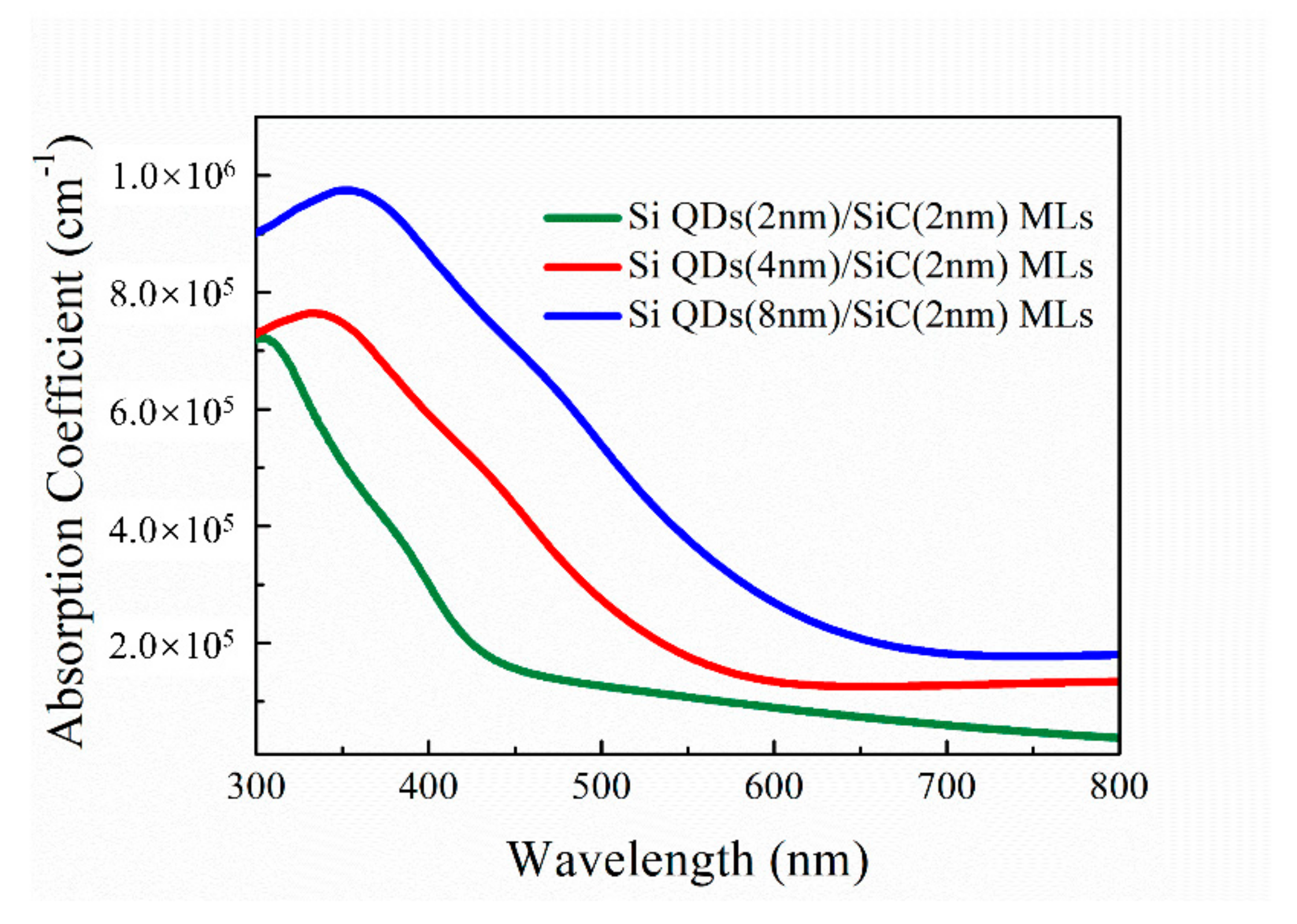
Measurement was conducted for the reflection and transmission of Si QDs/SiC MLs prepared on the quartz substrates so as to explore the optical performance of Si QDs/SiC MLs of different sizes. Figure 3 shows the deduced optical absorption coefficient in the 300–800 nm wavelength range. According to previous research results, the absorption of Si QDs/SiC MLs was almost unchanged through changing the thickness of SiC layers, indicating the dominance of Si QDs in optical absorption [30]. As shown in Figure 3, the optical absorption edge was shifted to the long wavelength region by raising the size of Si QDs. The red shifting behavior of the light absorption of Si QDs was already observed and discussed in Si QDs/SiNx, Si QDs/SiO2, and Si QDs/SiC MLs in our previous work [31,32,33], which was demonstrated in the result from QCE [34]. The optical bandgap (Egopt) can be extracted from Tauc’s function [35]. Si QDs/SiC MLs have a deduced Egopt of 2.0 eV, 1.5 eV, and 1.2 eV as dot size is 2.5 nm, 5.0 nm, and 8.9 nm, respectively. As discussed before, a modified model of effective-mass approximation (EMA) rather than an infinite barrier model was developed so as to predict the optical bandgap of Si QDs/SiC MLs through taking into account two terms including Coulomb effect and correlation energy [36]. Based on the EMA model, the calculated Egopt results are consistent with present experimental ones. It is worth noting that Si QDs with a size of 2.5 nm and 5.0 nm have an Egopt of about 2.0 eV and 1.5 eV, which is the theoretically desirable bandgaps of top and middle cell materials in three-junction tandem cells [6]. Moreover, it is demonstrated that the optical bandgap is tunable through changing the size of Si QDs due to QCE, thereby turning Si QDs/SiC multilayered structures into a good choice for future multi-junction TSC devices requiring controllable bandgap materials.
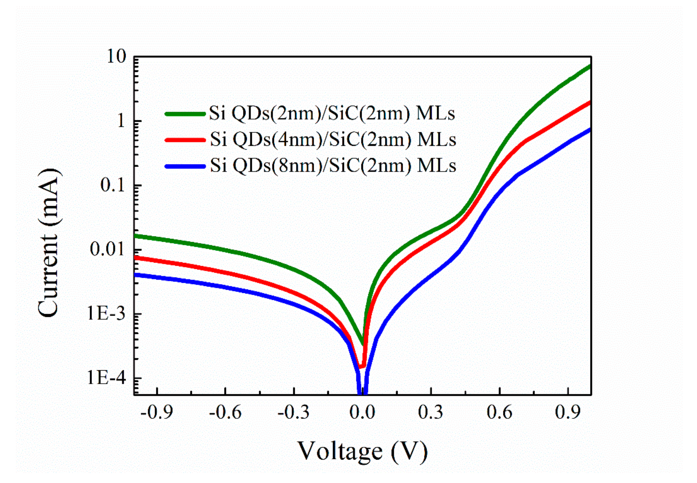
The current–voltage (I-V) relationship is measured in order to study the electronic characteristics of solar cell samples. Figure 4 presents the dark I-V relationship of different-sized Si QDs/SiC MLs-based solar cells. All samples have a rectification ratio of above 102 at ±1 V, indicating well-formed p-i-n structures in the present case. I-V characteristics can be divided into three parts. When V < 0.4 V (region 1), the I-V relationship is linearly dependent on the shunt resistor (Rsh). When 0.4 V < V < 0.6 V (region 2), current sees an exponential increase with forward voltage, which presents diode behavior. When V > 0.6 V (region 3), the I-V relationship deviates from the ideal behavior of diodes, which should be attributed to space-charge-limited current (SCLC) [37]. Especially in region 2, a standard diode relationship I∝exp(qV/nkT) can be used to fit I-V curves. Si QDs (2 nm, 4 nm, and 8 nm)/SiC MLs-based solar cell devices have a fitted ideality factor n of 2.47, 2.39, and 2.23, respectively, indicating that current is transported mainly via carrier tunneling [26]. As for the Si QDs/SiC stack model, its carrier tunneling probability (Te) is given by Equation (1) [6,38]:
where, d represents the distance between Si QDs (namely the thickness of SiC layer); m* refers to the effective mass of holes or electrons inside the barrier; ΔE stands for the height of the barrier between Si QDs and SiC (regarding electrons, for example, ΔE denotes the difference of energy between the conduction band edge of SiC and the confined energy level of Si QD = (Ec − En)). As mentioned earlier, Si QDs see an increase in bandgap with the decrease in their size, which thus reduces tunneling barrier height ΔE, as shown in Equation (1). Te will see a monotonic increase when the size of Si QDs reduces as all Si QDs/SiC MLs kept the same thickness d and m*, indicating that more holes and electrons will be able to tunnel via the barrier of SiC and then gathered by electrodes. Hence, dark current increases with the decreasing size of Si QDs, which is shown in Figure 4.
Figure 5 displays the J-V curves of different-sized Si QDs/SiC MLs-based solar cells under illumination. Device parameters including Jsc, open-circuit voltage (Voc), fill factor (FF), and PCE are summarized in Table 1. Since the device performance of solar cells is greatly dependent on collection efficiency and photo-generated carrier tunneling, the sample containing 2-nm-sized Si QDs shows the highest Jsc. However, keeping the thickness of the active layers of cells with smaller-sized Si QDs meant increasing the periodicity of MLs in this experimental design. As a result, Si QDs (2 nm)/SiC MLs have the largest periodicity of 12, whose corresponding cell exhibits the lowest Voc on account of the strong interface recombination resulting from the increased total number of layers. In addition, previous research indicated that SiC had a conductivity of ~10−10 S/cm, four orders of magnitude lower compared with Si QDs layers [39]. Thus, solar cells see an increase in contact resistance when the number of SiC sublayers increases, thereby leading to a decline in FF. Consequently, solar cells with 2-nm-sized Si QDs only have a PCE of 4.59%. In this work, all the effects mentioned above are taken into consideration. When Si QDs sublayers have a thickness of 4 nm, solar cells achieve the best photovoltaic property, whose PCE is 7.27%. Notably, no optimization has been conducted for the parameters of present cells, because defects at junction interfaces were reported to form during the process of high-temperature annealing, playing the role of recombination centers and leading to a drop in Jsc and FF [26]. The layer-by-layer treatment of hydrogen plasma may be a method of passivating defects and further improving the performance of solar cells [40].
Figure 6a shows the EQE spectra of different-sized Si QDs/SiC MLs-based solar cells. The spectral response wavelength shows a red shift to the region of long wavelength when the size of Si QDs increases. For example, EQE has a decline of about 20% at the wavelength of around 500 nm when the size of Si QDs increases from 2 nm to 8 nm mainly due to the spectral mismatch and poorer response of larger Si QDs in the region of short wavelength. According to the above discussion, however, the EQE results revealed that the substrate of c-Si absorbed most incident light in such structured solar cell structures [41]. The heavily-doped (p+-Si, ~0.001 Ω•cm) substrate rather than the p-Si (1~3 Ω•cm) substrate was used to obtain solar cell devices, with an eye to excluding the absorption of incident light by the c-Si substrate and further investigating what Si QDs contribute to spectral response. It is known that heavily-doped semiconductors have been acting as “death layers” in solar cells because of not contributing to photo-generated carriers due to short minority carrier lifetime and high recombination rate [42]. As shown in Figure 6b, p+-i-n devices with Si QDs/SiC MLs of different sizes have a quite low EQE in the region of near-infrared (NIR) light from 800 nm to 1200 nm, which is because photocurrent cannot be generated by the light of long wavelength absorbed in heavily-doped substrates. Meanwhile, it is observed that cell devices whose Si QDs have a size of 2 nm, 4 nm, and 8 nm exhibit the peaks of EQE spectra located at 460 nm, 500 nm, and 530 nm, respectively. It shows that spectral response is red shifted to the long wavelength region when Si QDs sees an increase in size, which may result from the reducing bandgap of Si QDs owing to QCE. In terms of the EQE results, Equation (2) can be used for calculating Jsc obtained from the spectral response of solar cells in various wavelength ranges:
where, q is the charge of electrons and is incident photon flux. Solar cells whose Si QDs have the size of 2 nm, 4 nm, and 8 nm obtain an integrated Jsc of 9.19 mA/cm2, 8.65 mA/cm2, and 7.32 mA/cm2, respectively, which can result from the spectral response of Si QDs.
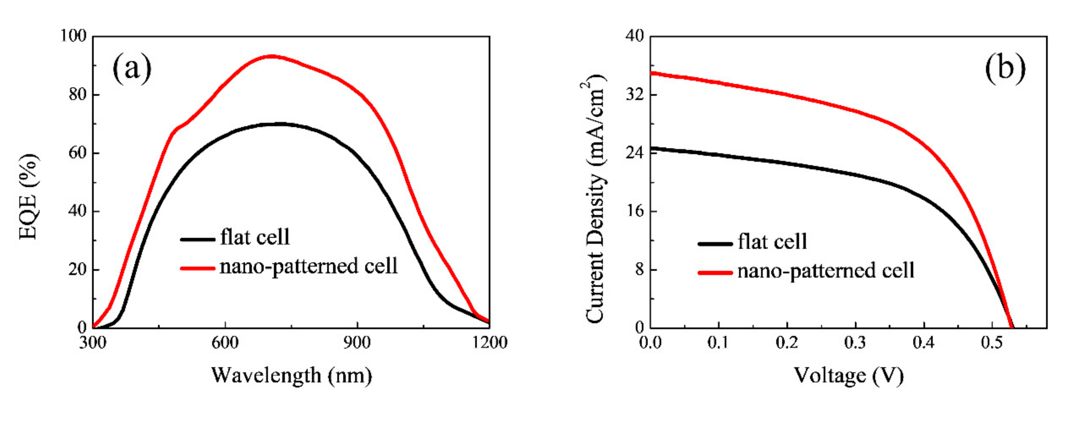
It has been reported that light trapping nanostructures can be introduced to greatly enhance the photovoltaic performance of solar cells [43]. In previous research, nano-sphere lithography and an RIE technique were developed to get Si-based nanostructures owning good anti-reflective property [27,44,45]. In the present work, HSCs were formed by preparing Si QDs (4 nm)/SiC MLs on the substrate of nano-patterned Si in order to achieve high-efficiency solar cells based on Si QDs. The formed structure of nano-patterned solar cell was analyzed by SEM and TEM measurement. Figure 7a clearly identifies periodically Si nano-cone structures. The inset of Figure 7a shows that nano-cone has a lateral size of around 300 nm and a depth of around 120 nm after undergoing 8 min etching, which is in well agreement with the previous results [27]. It is worth noting that Si QDs/SiC MLs remain unchanged on the nano-patterned substrate, which indicates a process of conformal deposition in PECVD system. Reflection spectra of solar cells based on Si QDs fabricated on the substrates of nano-patterned and flat p-Si are presented in Figure 7b. It is observed that nano-patterned solar cells have significant anti-reflection effect in the whole spectral range. Meanwhile, the mean reflection weighted by the solar spectrum under the illumination of AM1.5G in the wavelength range between 300 nm and 1200 nm sees a decrease of 39.1% to 8.9% through the formation of present nano-patterned solar cells, decreasing by 77.2% compared with flat cells.
EQE spectra of nano-patterned and flat devices are shown in Figure 8a. Nano-patterned cells show an obvious increase in the whole spectral range compared with flat ones, which can be attributable to the improved optical absorption caused by the anti-reflection property of nano-patterned structures, as illustrated in Figure 7b. As a result, Jsc increases to 34.95 mA/cm2, which is shown in Figure 8b. Moreover, Voc and FF results of nano-patterned cells are almost the same as those of flat ones, since the periodically Si nano-patterned substrate and Si QDs/SiC MLs have been found to be well kept after fabrication process. Correspondingly, Si QDs (4 nm)/SiC MLs-based nano-patterned solar cells exhibit an improved PCE of 10.15%. In this study, the size-dependent and improved photovoltaic property of different-sized Si QDs/SiC MLs-based solar cells are studied and demonstrated in a systematic way. The experimental results show consistency with the values of Si QDs/SiO2 MLs or Si QDs/SiNx MLs reported in other groups, and even greater than those of p-type Si QDs: SiC/n-type c-Si solar cells as p-i-n structures are used to avoid the diffusion of dopants in the p-n junction. This work demonstrates that Si QDs/SiC MLs can be applied in third-generation Si TSCs, particularly solar cells based on all-Si QDs. To meet the demand of photovoltaic technology development for low cost, solar cells based on all-Si QDs films will significantly reduce the cost of traditional c-Si and poly-Si solar panels in their future application.
4. Conclusions
In this work, a-Si:H/SiC MLs are annealed at 900 °C to fabricate solar cells based on Si QDs/SiC MLs. The designed thickness of a-Si:H sublayers is 2 nm, 4 nm, and 8 nm, while that of amorphous SiC sublayers is 2 nm. According to TEM and Raman observation, Si QDs are successfully achieved after annealing with a diameter of 2.5 nm, 5.0 nm, and 8.9 nm, indicating that the size of Si QDs is controllable. A study on the optical performance of Si QDs/SiC MLs shows that optical absorption edge has a red shift to the long wavelength region when the size of Si QDs increases, which is due to QCE. Moreover, HSCs are obtained by fabricating Si QDs/SiC MLs of different sizes and phosphorus-doped a-Si films on the substrates of p-Si and p+-Si. The results indicate that the photovoltaic performance of Si QDs is strongly dependent on their size, and solar cells with Si QDs (4 nm)/SiC (2 nm) MLs have the best photovoltaic parameters of Voc, Jsc, and PCE, which are 530 mV, 24.66 mA/cm2, and 7.27%, respectively. EQE measurement of p+-i-n devices excluding the absorption of the c-Si substrate clearly demonstrates what Si QDs contribute to spectral response in the region of UV-Vis light. The spectral response in the short wavelength region is enhanced with the decreasing size of Si QDs from 8 nm to 2 nm, which is in well agreement with QCE. Furthermore, the PCE of nano-patterned solar cells significantly increases to 10.15% by depositing Si QDs (4 nm)/SiC MLs on the Si light trapping substrate. According to the experimental results, it is inferred that Si QDs/SiC MLs of controllable sizes will be potentially applied to get a better spectral match for advanced high-efficiency photovoltaic devices.
Author Contributions
Conceptualization, Y.C. and D.S.; methodology, Y.C., P.Z. and D.L.; investigation, Y.C., D.S. and P.Z.; writing—original draft preparation, Y.C. and P.Z.; writing—review and editing, D.L. and X.Z.; funding acquisition, Y.C. and D.S. All authors have read and agreed to the published version of the manuscript.
Funding
This work was supported by the National Natural Science Foundation of China (NSFC, No. 61704148), NSF of Jiangsu Province (No. BK20170514), Postdoctoral Research Grant Program of Jiangsu Province [No. 2020Z269 and 2020Z403], China Postdoctoral Science Foundation [No. 2019M651750 and 2020M671438], Jiangsu Overseas Research & Training Program for University Prominent Young & Middle-Aged Teachers and Presidents, Jiangsu Province Jiangsu Province Industry-University-Research Cooperation Project [No. BY2019248] and “Qing Lan Project” of Jiangsu Province [2018 and 2020].
Conflicts of Interest
The authors declare no conflict of interest.
References
- Shockley, W.; Queisser, H.J. Detailed balance limit of efficiency of p-n junction solar cells. J. Appl. Phys. 1961, 32, 510–519. [Google Scholar] [CrossRef]
- Green, M.A. Third Generation Photovoltaics: Advanced Solar Energy Conversion; Springer: Berlin, Germany, 2003; pp. 35–66. [Google Scholar]
- Yamamoto, A.; Tsujino, M.; Ohkubo, M.; Hashimoto, A. Metalorganic chemical vapor deposition growth of InN for InN/Si tandem solar cell. Sol. Energy Mater. Sol. Cells 1994, 35, 53–60. [Google Scholar] [CrossRef]
- Lunardi, M.M.; Moore, S.; Alvarez-Gaitan, J.P.; Yan, C.; Hao, X.J.; Corkish, R. A comparative life cycle assessment of chalcogenide/Si tandem solar modules. Energy 2018, 145, 700–709. [Google Scholar] [CrossRef]
- Meillaud, F.; Shah, A.; Droz, C.; Vallat-Sauvain, E.; Miazza, C. Efficiency limits for single-junction and tandem solar cells. Sol. Energy Mater. Sol. Cells 2006, 90, 2952–2959. [Google Scholar] [CrossRef] [Green Version]
- Conibeer, G.; Green, M.; Cho, E.C.; Konig, D.; Cho, Y.H.; Fangsuwannarak, T.; Scardera, G.; Pink, E.; Huang, Y.D.; Puzzer, T.; et al. Silicon quantum dot nanostructures for tandem photovoltaic cells. Thin Solid Films 2008, 516, 6748–6756. [Google Scholar]
- Baba, M.; Makita, K.; Mizuno, H.; Takato, H.; Sugaya, T.; Yamada, N. Effect of series resistances on conversion efficiency of GaAs/Si tandem solar cells with areal current-matching technique. IEEE J. Photovolt. 2018, 8, 654–660. [Google Scholar]
- Hajijafarassar, A.; Martinho, F.; Stulen, F.; Grini, S.; López-Mariño, S.; Espíndola-Rodríguez, M.; Döbeli, M.; Canulescu, S.; Stamate, E.; Gansukh, M.; et al. Monolithic thin-film chalcogenide-silicon tandem solar cells enabled by a diffusion barrier. Sol. Energy Mater. Sol. Cells 2020, 207, 110334. [Google Scholar] [CrossRef]
- Moritz, H.; Futscher, B.E. Efficiency limit of perovskite/Si tandem solar cells. ACS Energy Lett. 2016, 1, 863–868. [Google Scholar]
- Taguchi, H.; Soga, T.; Jimbo, T. Fabrication of GaAs/Si tandem solar cell by epitaxial lift-off technique. Jpn. J. Appl. Phys. 2003, 42, 1419–1421. [Google Scholar] [CrossRef]
- Kim, B.; Toprasertpong, K.; Paszuk, A.; Supplie, O.; Nakano, Y.; Hannappel, T.; Sugiyama, M. GaAsP/Si tandem solar cells: Realistic prediction of efficiency gain by applying strain-balanced multiple quantum wells. Sol. Energy Mater. Sol. Cells 2018, 180, 303–310. [Google Scholar]
- Essig, S.; Steiner, M.A.; Allebé, C.; Geisz, J.F.; Paviet-Salomon, B.; Ward, S.; Descoeudres, A.; LaSalvia, V.; Barraud, L.; Badel, N.; et al. Realization of GaInP/Si dual-junction solar cells with 29.8% 1-sun efficiency. IEEE J. Photovolt. 2016, 6, 1012–1019. [Google Scholar] [CrossRef]
- He, C.; Han, C.B.; Xu, Y.R.; Li, X.J. Photovoltaic effect of CdS/Si nanoheterojunction array. J. Appl. Phys. 2011, 110, 094316. [Google Scholar] [CrossRef]
- Carmody, M.; Mallick, S.; Margetis, J.; Kodama, R.; Biegala, T.; Xu, D.; Bechmann, P.; Garland, J.W.; Sivananthan, S. Single-crystal II-VI on Si single-junction and tandem solar cells. Appl. Phys. Lett. 2010, 96, 153502. [Google Scholar] [CrossRef]
- Leijtens, T.; Bush, K.A.; Prasanna, R.; McGehee, M.D. Opportunities and challenges for tandem solar cells using metal halide perovskite semiconductors. Nat. Energy 2018, 3, 828–838. [Google Scholar] [CrossRef]
- Qiu, Z.W.; Xu, Z.Q.; Li, N.X.; Zhou, N.; Chen, Y.H.; Wan, X.X.; Liu, J.L.; Li, N.; Hao, X.T.; Bi, P.Q.; et al. Monolithic perovskite/Si tandem solar cells exceeding 22% efficiency via optimizing top cell absorber. Nano Energy 2018, 53, 798–807. [Google Scholar] [CrossRef]
- Jiang, Y.J.; Almansouri, I.; Huang, S.J.; Young, T.; Li, Y.; Peng, Y.; Hou, Q.C.; Spiccia, L.; Bach, U.; Cheng, Y.B.; et al. Optical analysis of perovskite/silicon tandem solar cells. J. Mater. Chem. C 2016, 4, 5679–5689. [Google Scholar] [CrossRef]
- Conibeer, G.; Perez-Wurfl, I.; Hao, X.J.; Di, D.W.; Lin, D. Si solid-state quantum dot-based materials for tandem solar cells. Nanoscale Res. Lett. 2012, 7, 193. [Google Scholar] [CrossRef] [Green Version]
- Cheng, Q.J.; Tam, E.; Xu, S.Y.; Ostrikov, K. Si quantum dots embedded in an amorphous SiC matrix: Nanophase control by non-equilibrium plasma hydrogenation. Nanoscale 2010, 2, 594–600. [Google Scholar] [CrossRef] [Green Version]
- Heitmann, J.; Muller, F.; Zacharias, M.; Gosele, U. Silicon nanocrystals: Size matters. Adv. Mater. 2005, 17, 795–803. [Google Scholar] [CrossRef]
- Uchida, G.; Yamamoto, K.; Sato, M.; Kawashima, Y.; Nakahara, K.; Kamataki, K.; Itagaki, N.; Koga, K.; Shiratani, M. Effect of nitridation of Si nanoparticles on the performance of quantum-dot sensitized solar cells. Jpn. J. Appl. Phys. 2012, 51, 01AD01. [Google Scholar] [CrossRef]
- Chang, G.R.; Ma, F.; Ma, D.Y.; Xu, K.W. Multi-band silicon quantum dots embedded in an amorphous matrix of silicon carbide. Nanotechnology 2010, 21, 465605. [Google Scholar] [PubMed]
- Cho, E.C.; Park, S.W.; Hao, X.J.; Song, D.Y.; Conibeer, G.; Park, S.C.; Green, M.A. Silicon quantum dot/crystalline silicon solar cells. Nanotechnology 2008, 19, 245201. [Google Scholar] [PubMed]
- Chen, X.B.; Yang, W.; Yang, P.Z.; Yuan, J.B.; Zhao, F.; Hao, J.B.; Tang, Y. Size-controlled Si quantum dots embedded in B-doped SiNx/Si3N4 superlatice for Si quantum dot solar cells. J. Mater. Sci. Mater. Electron. 2017, 28, 1322–1327. [Google Scholar]
- Cho, E.C.; Green, M.A.; Conibeer, G.; Song, D.Y.; Cho, Y.H.; Scardera, G.; Huang, S.J.; Park, S.W.; Hao, X.J.; Huang, Y.D.; et al. Silicon quantum dots in a dielectric matrix for all-silicon tandem solar cells. Adv. OptoElectron. 2007, 15, 69578. [Google Scholar]
- Song, D.Y.; Cho, E.C.; Conibeer, G.; Flynn, C.; Huang, Y.D.; Green, M.A. Structural, electrical and photovoltaic characterization of Si nanocrystals embedded SiC matrix and Si nanocrystals/c-Si heterojunction. Sol. Energy Mater. Sol. Cells 2008, 92, 474–481. [Google Scholar]
- Shao, W.Y.; Lu, P.; Li, W.; Xu, J.; Xu, L.; Chen, K.J. Simulation and experimental study on anti-reflection characteristics of nano-patterned Si structures for Si quantum dot-based light-emitting devices. Nanoscale Res. Lett. 2016, 11, 317. [Google Scholar]
- Tsu, R.; Gonzalez-Hernandez, J.; Chao, S.S.; Lee, S.C.; Tanaka, K. Critical volume fraction of crystallinity for conductivity percolation in phosphorus-doped Si:F:H alloys. Appl. Phys. Lett. 1982, 40, 534–535. [Google Scholar]
- Campbell, I.H.; Fauchet, P.M. The effects of microcrystal size and shape on the one phonon Raman spectra of crystalline semiconductors. Solid State Commun. 1986, 58, 739–741. [Google Scholar]
- Cao, Y.Q.; Xu, X.; Li, S.X.; Li, W.; Xu, J.; Chen, K.J. Improved photovoltaic properties of Si quantum dots/SiC multilayers-based heterojunction solar cells by reducing tunneling barrier thickness. Front. Optoelectron. 2013, 6, 228–233. [Google Scholar]
- Zhang, P.; Zhang, X.W.; Xu, J.; Mu, W.W.; Xu, J.; Li, W.; Chen, K.J. Tunable nonlinear optical properties in nanocrystalline Si/SiO2 multilayers under femtosecond excitation. Nanoscale Res. Lett. 2014, 9, 28. [Google Scholar]
- Wu, W.; Huang, X.F.; Chen, K.J.; Xu, J.B.; Gao, X.; Xu, J.; Li, W. Room temperaturevisible electroluminescence in silicon nanostructures. J. Vac. Sci. Technol. A 1999, 17, 159–163. [Google Scholar] [CrossRef]
- Rui, Y.J.; Li, S.X.; Cao, Y.Q.; Xu, J.; Li, W.; Chen, K.J. Structural and electroluminescent properties of Si quantum dots/SiC multilayers. Appl. Surf. Sci. 2013, 269, 37–40. [Google Scholar] [CrossRef]
- Priolo, F.; Gregorkiewicz, T.; Galli, M.; Krauss, T.F. Silicon nanostructures for photonics and photovoltaics. Nat. Nanotechnol. 2014, 9, 19–32. [Google Scholar] [CrossRef]
- Tauc, J.; Grigorovici, R.; Vancu, A. Optical properties and electronic structure of amorphous germanium. Phys. Status Solidi 1966, 15, 627–637. [Google Scholar] [CrossRef]
- Rui, Y.J.; Li, S.X.; Xu, J.; Song, C.; Jiang, X.F.; Li, W.; Chen, K.J.; Wang, Q.M.; Zuo, Y.H. Size-dependent electroluminescence from Si quantum dots embedded in amorphous SiC matrix. J. Appl. Phys. 2011, 110, 064322. [Google Scholar] [CrossRef]
- Park, S.; Cho, E.C.; Song, D.Y.; Conibeer, G.; Green, M.A. n-Type silicon quantum dots and p-type crystalline silicon heteroface solar cells. Sol. Energy Mater. Sol. Cells 2009, 93, 684–690. [Google Scholar] [CrossRef]
- Boer, K. Survey of Semiconductor Physics; Van Nostrand Reinhold: New York, NY, USA, 1990; p. 244. [Google Scholar]
- Song, C.; Rui, Y.J.; Wang, Q.B.; Xu, J.; Li, W.; Chen, K.J.; Zuo, Y.H.; Wang, Q.M. Structural and electronic properties of Si nanocrystals embedded in amorphous SiC matrix. J. Alloy. Compd. 2011, 509, 3963–3966. [Google Scholar] [CrossRef]
- Li, S.X.; Cao, Y.Q.; Xu, J.; Rui, Y.J.; Li, W.; Chen, K.J. Hydrogenated amorphous silicon-carbide thin films with high photo-sensitivity prepared by layer-by-layer hydrogen annealing technique. Appl. Surf. Sci. 2013, 270, 287–291. [Google Scholar] [CrossRef]
- Cao, Y.Q.; Lu, P.; Zhang, X.W.; Xu, J.; Xu, L.; Chen, K.J. Enhanced photovoltaic property by forming p-i-n structures containing Si quantum dots/SiC multilayers. Nanoscale Res. Lett. 2014, 9, 634. [Google Scholar] [CrossRef] [Green Version]
- Tyagi, M.S.; Van Overstraeten, R. Minority carrier recombination in heavily-doped silicon. Solid-State Electron. 1983, 26, 577–597. [Google Scholar] [CrossRef]
- Zhu, J.; Hsu, C.M.; Yu, Z.F.; Fan, S.H.; Cui, Y. Nanodome solar cells with efficient light management and self-cleaning. Nano Lett. 2010, 10, 1979–1984. [Google Scholar] [CrossRef]
- Xu, J.; Sun, S.H.; Cao, Y.Q.; Lu, P.; Li, W.; Chen, K.J. Light trapping and down-shifting effect of periodically nanopatterned Si-quantum-dot-based structures for enhanced photovoltaic properties. Part. Part. Syst. Charact. 2014, 31, 459–464. [Google Scholar] [CrossRef]
- Lu, P.; Xu, J.; Cao, Y.Q.; Lai, J.W.; Xu, L.; Chen, K.J. Preparation of nano-patterned Si structures for hetero-junction solar cells. Appl. Surf. Sci. 2015, 334, 123–128. [Google Scholar] [CrossRef]
Figure 1.
Cross-section TEM images of (a) a-Si (2 nm)/a-SiC (2 nm) multilayers (MLs); (b) a-Si (4 nm)/a-SiC (2 nm) MLs; (c) a-Si (8 nm)/a-SiC (2 nm) MLs; (d) Si quantum dots (QDs) (2 nm)/SiC (2 nm) MLs; (e) Si QDs (4 nm)/SiC (2 nm) MLs; (f) Si QDs (8 nm)/SiC (2 nm) MLs.
Figure 1.
Cross-section TEM images of (a) a-Si (2 nm)/a-SiC (2 nm) multilayers (MLs); (b) a-Si (4 nm)/a-SiC (2 nm) MLs; (c) a-Si (8 nm)/a-SiC (2 nm) MLs; (d) Si quantum dots (QDs) (2 nm)/SiC (2 nm) MLs; (e) Si QDs (4 nm)/SiC (2 nm) MLs; (f) Si QDs (8 nm)/SiC (2 nm) MLs.

Figure 2.
Raman spectra of Si QDs/SiC MLs undergoing annealing at 900 °C.

Figure 3.
Spectra of optical absorption coefficients of Si QDs/SiC MLs.

Figure 4.
Dark I-V curves of different-sized Si QDs/SiC MLs-based solar cells.

Figure 5.
J-V curves of solar cells with Si QDs/SiC MLs of different sizes under the illumination of AM1.5G.
Figure 5.
J-V curves of solar cells with Si QDs/SiC MLs of different sizes under the illumination of AM1.5G.

Figure 6.
External quantum efficiency (EQE) spectra of (a) p-i-n; (b) p+-i-n structured solar cells with different-sized Si QDs/SiC MLs.
Figure 6.
External quantum efficiency (EQE) spectra of (a) p-i-n; (b) p+-i-n structured solar cells with different-sized Si QDs/SiC MLs.

Figure 7.
(a) SEM image of Si QDs/SiC MLs on the substrate of nano-patterned Si. Cross-section TEM image is in the inset of Figure 7a; (b) reflection spectra of Si QDs/SiC MLs-based solar cells on flat and nano-patterned substrates.
Figure 7.
(a) SEM image of Si QDs/SiC MLs on the substrate of nano-patterned Si. Cross-section TEM image is in the inset of Figure 7a; (b) reflection spectra of Si QDs/SiC MLs-based solar cells on flat and nano-patterned substrates.

Figure 8.
(a) EQE spectra and (b) AM1.5G illuminated J-V curves of Si QDs/SiC MLs-based solar cells on flat and nano-patterned substrates.
Figure 8.
(a) EQE spectra and (b) AM1.5G illuminated J-V curves of Si QDs/SiC MLs-based solar cells on flat and nano-patterned substrates.


Table 1.
Device parameters of different-sized Si QDs/SiC MLs-based solar cells.
| Voc (mV) | Jsc (mA/cm2) | FF (%) | PCE (%) | |
|---|---|---|---|---|
| Si QDs(2 nm)/SiC(2 nm) MLs | 425 ± 10 | 25.02 ± 0.85 | 43.2 ± 1.3 | 4.59 ± 0.31 |
| Si QDs(4 nm)/SiC(2 nm) MLs | 530 ± 9 | 24.66 ± 0.82 | 55.6 ± 1.5 | 7.27 ± 0.45 |
| Si QDs(8 nm)/SiC(2 nm) MLs | 532 ± 9 | 21.75 ± 0.75 | 55.8 ± 1.7 | 6.45 ± 0.37 |
© 2020 by the authors. Licensee MDPI, Basel, Switzerland. This article is an open access article distributed under the terms and conditions of the Creative Commons Attribution (CC BY) license (http://creativecommons.org/licenses/by/4.0/).
Share and Cite
MDPI and ACS Style
Cao, Y.; Zhu, P.; Li, D.; Zeng, X.; Shan, D. Size-Dependent and Enhanced Photovoltaic Performance of Solar Cells Based on Si Quantum Dots. Energies 2020, 13, 4845. https://doi.org/10.3390/en13184845
AMA Style
Cao Y, Zhu P, Li D, Zeng X, Shan D. Size-Dependent and Enhanced Photovoltaic Performance of Solar Cells Based on Si Quantum Dots. Energies. 2020; 13(18):4845. https://doi.org/10.3390/en13184845
Chicago/Turabian StyleCao, Yunqing, Ping Zhu, Dongke Li, Xianghua Zeng, and Dan Shan. 2020. "Size-Dependent and Enhanced Photovoltaic Performance of Solar Cells Based on Si Quantum Dots" Energies 13, no. 18: 4845. https://doi.org/10.3390/en13184845
Note that from the first issue of 2016, this journal uses article numbers instead of page numbers. See further details here.