
CdTe-Based Thin Film Solar Cells: Past, Present and Future


Laboratory for Photovoltaics and Solid-State Physics (LAPS), Department of Computer Science, University of Verona, Ca’ Vignal 1, Strada Le Grazie 15, 37134 Verona, Italy
*
Author to whom correspondence should be addressed.
Energies 2021, 14(6), 1684; https://doi.org/10.3390/en14061684
Submission received: 9 February 2021
/
Revised: 9 March 2021
/
Accepted: 12 March 2021
/
Published: 18 March 2021
(This article belongs to the Special Issue Photovoltaic Devices)
Abstract
:CdTe is a very robust and chemically stable material and for this reason its related solar cell thin film photovoltaic technology is now the only thin film technology in the first 10 top producers in the world. CdTe has an optimum band gap for the Schockley-Queisser limit and could deliver very high efficiencies as single junction device of more than 32%, with an open circuit voltage of 1 V and a short circuit current density exceeding 30 mA/cm2. CdTe solar cells were introduced at the beginning of the 70s and they have been studied and implemented particularly in the last 30 years. The strong improvement in efficiency in the last 5 years was obtained by a new redesign of the CdTe solar cell device reaching a single solar cell efficiency of 22.1% and a module efficiency of 19%. In this paper we describe the fabrication process following the history of the solar cell as it was developed in the early years up to the latest development and changes. Moreover the paper also presents future possible alternative absorbers and discusses the only apparently controversial environmental impacts of this fantastic technology.
1. Introduction
CdTe solar cell thin film photovoltaic technology was introduced in the early seventies of the last century [1] and it is now the only thin film technology in the first 10 top producers in the world [2].
This is because CdTe is a very robust and highly chemically stable and, also for this reason, can be deposited with a large variety of methods available making it very much ideal for production in large area.
CdTe has an optimum band gap near 1.5 eV according to the Schockley-Queisser limit so that it could deliver efficiencies around 32%, with an open circuit voltage of more than 1 V and a short circuit current density of more than 30 mA/cm2 [3].
CdTe solar cells were introduced for the first time in 1972, by Bonnet and Rabenhorst [1], with a CdS/CdTe heterojunction delivering a 6% efficiency. Since then, thin film CdTe based solar cells have been fabricated with this type of heterojunction until it has been radically changed in the recent years.
A series of improving steps introduced (among them: high substrate temperature during CdTe deposition, CdCl2 activation treatment, copper doping) brought to high conversion factors above 15%. Ferekides et al. [4] demonstrated an efficiency of 15.8%, followed by the 16.5% record which was obtained at the National Renewable Energy Laboratories (NREL) by Wu et al. [5].
The strong improvement in efficiency in the last 5 years was obtained by a new redesign of the CdTe solar cell device, removing CdS and considering new features such as band gap grading, copper embedding, and more transparent n-layer. With these changes First Solar have delivered a 21.5% efficiency device [6] later improved to 22.1% [7], the stunning fact is that these results have been gained from materials obtained from the production line. This demonstrates the high potential in terms of scalability of this technology, in fact a large area module of 19% has been delivered [7]. In the next sections both old and new configuration of the CdTe solar cell will be described.
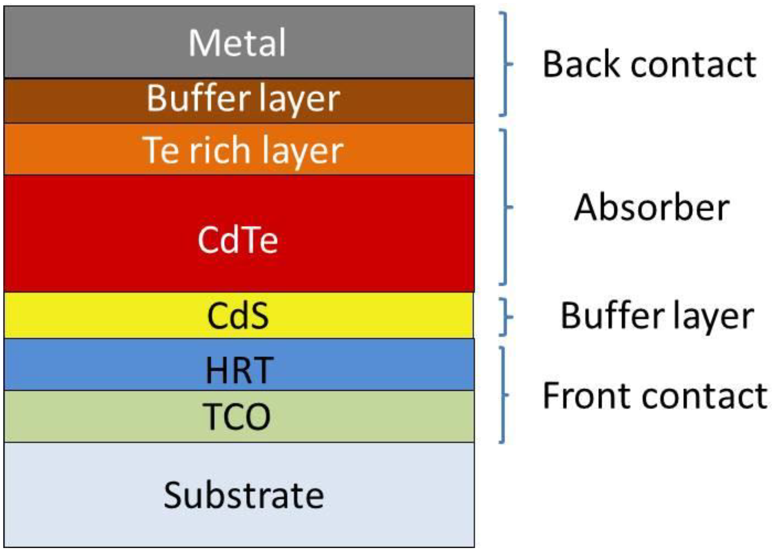
Like many other thin film technologies, CdTe solar cells can be fabricated in a way where the sunlight passes through the supporting glass or not, in the first case the cell is fabricated in superstrate configuration, in the second case in substrate configuration (see Figure 1).
However for CdTe devices, superstrate configuration is the best option in terms of efficiency, mainly because this structure allows the necessary post deposition treatment to be effective, more details will be reported forward. In this case, the window and absorber layers (respectively CdS and CdTe) are grown on the front contact, which is a degenerately doped semiconductor, typically an oxide layer, defined as transparent conducting-oxide (TCO). The supporting substrate is preferably a low-cost soda-lime glass when the growth is obtained at substrate temperatures below 450 °C, otherwise a more expensive alkali-free glass needs to be applied in case of high substrate temperature growth (above 500 °C).
In substrate configuration instead, the first layer that coats the substrate is usually molybdenum, a stable metal that works as an efficient back contact and at the same time avoids diffusion of impurities in the subsequent layers. One important benefit of this configuration is the possibility of using opaque substrates; so instead of using glass, one can apply flexible materials such as thin metal foils or polymers and deliver a flexible device [8]. At the moment, in substrate configuration, record efficiency for flexible CdTe cells is 13.6% on a Mo/MoOx coated glass substrate [9], while on flexible polymer foils with a MoOx/Te back contact is 11.5% with copper and 10.9% without, if deposited on steel substrates [9]. In superstrate configuration it is also possible to perform flexible CdTe solar cells either by the application of a special flexible polymer or ultra-thin flexible glass [10].
2. The Past and Present: CdTe/CdS Solar Cell Configuration
For a very long period of time up to 2015, CdTe solar cells have been prepared in superstrate configuration by depositing subsequently on glass substrate a transparent conductive oxide, a CdS layer, the CdTe as absorber layer, and finally the back contact.
For thin films the substrate represents more than 98% of the material so it is necessary to choose a low cost material such as soda lime glass in order limit the costs. However soda lime glass is limited by the presence of sodium and potassium that can diffuse into the device degrading it and that make the glass soft at temperatures above 500 °C. We now describe all the different layers that compose the standard configuration, the majority of these is still used in the new configuration that will be shown in Section 3.
2.1. The Front Contact
The front-contact must be a highly degenerative conductive semiconductor which is at the same time transparent (high band-gap) and conductive (highly doped): transparent conductive oxides (TCO).
However oxides are generally intrinsic materials, so in order to increase the n-conductivity donor elements are introduced to substitute the higher valence cation with donor impurities. In this way TCOs are degenerate semiconductors with a carrier concentration in the range of 1018 cm−3–1020 cm−3.
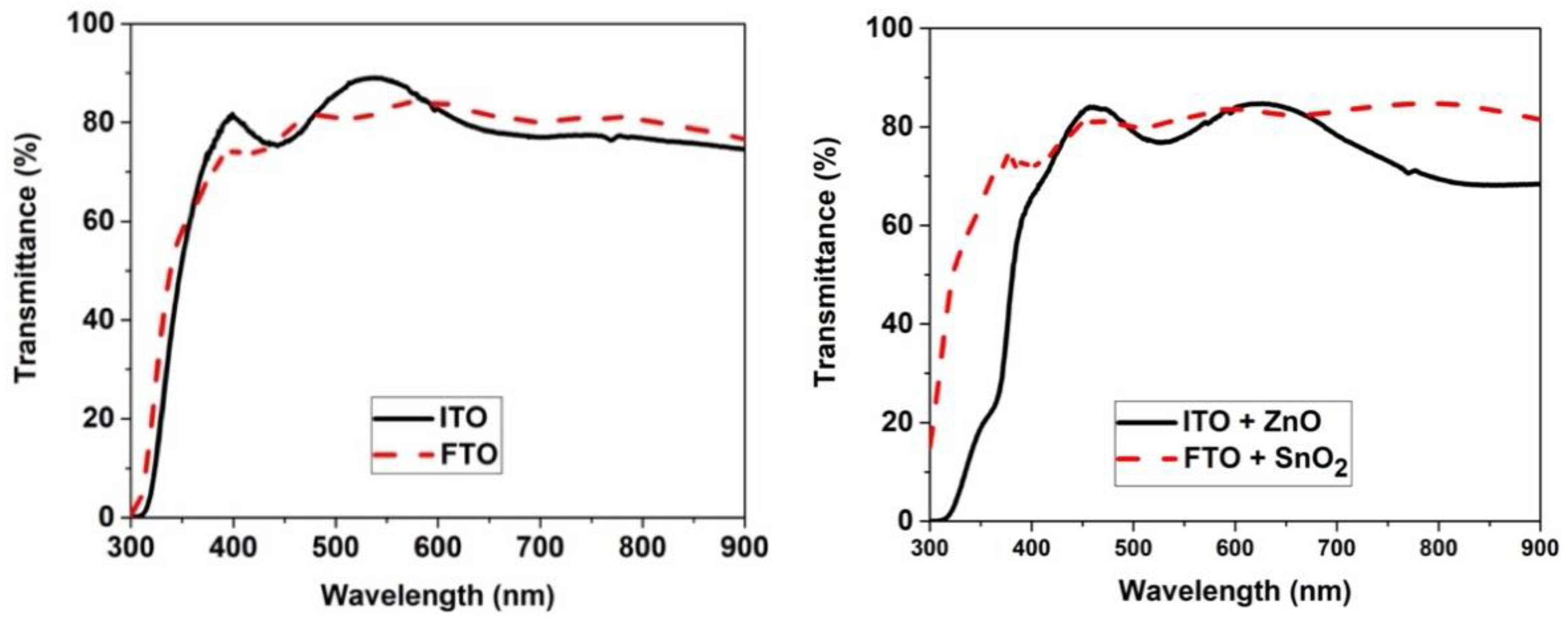
There is a very wide variety of TCOs for CdTe solar cells, however the most used are: SnO2:F (FTO), ZnO:Al (AZO) and In2O3:Sn (ITO). More sophisticated TCOs have been used, such as Cd2SnO4 (CTO) [5], in order to improve conductivity and transparency and perform higher efficiency. However, in a large-scale production, materials that can be easily deposited on large areas are preferred; typically FTO is widely used due to its properties of stability in the long period.
Also intrinsic oxides (high resistant transparent layers: HRT), with their electrical resistivity in the range of 102–105 Ωcm, are deposited on the TCO and CdS in order to (1) avoid shunting of the device often generated by micro-pinholes from thin buffer layers and (2) generate an optimized alignment of the energy bands. These allow the thinning of the CdS layer, reducing its parasitic absorbance, and thus gaining energy in the wavelength range below 500 nm. Most applied HRTs are TO (tin oxide) or ZnO (zinc oxide) (see Figure 2) [11].
In superstrate configuration, the TCO is the first layer deposited on glass and they can influence the morphology and structure of the subsequent films. It is very important to control possible impurities that can diffuse from the TCO inside the device at the junction. It has been actually observed that the structure of the TCO affects both the CdS and the CdTe grain structure and consequentially their electrical properties [12,13] so it can be concluded that the requirements for TCOs must also comprise their chemical and physical stability [14]. We describe more in detail the most widespread materials for front contact.
2.1.1. Indium Tin Oxide
The most diffused type of TCO in the family of In2O3 (IO) based thin films is the indium tin oxide (ITO). Its band gap is, depending on the deposition parameters, ranging from 3.55 to 3.75 eV, with a transparency from the visible to the near infrared regions exceeding 80% (see Figure 2). These layers grow in polycrystalline form with a cubic structure and the grains size can range between 10 and 50 nm depending on the deposition technique and substrate temperature. Generally IO films can be deposited by reactive R.F. sputtering, activated reactive evaporation, chemical vapour deposition and also spray pyrolysis.
2.1.2. Zinc Oxides
Zinc oxide, with a band gap of 3.2 eV, is mainly used as a high resistive layer between ITO and CdS in order to increase the open circuit voltage. However ZnO can be doped with indium or with aluminium obtaining a high conductive and transparent layer: in particular aluminium doping is perfect to be applied for high conductivity [15,16]. Typically ZnO layers are deposited by radio frequency sputtering. The films, polycrystalline, show a wurtzite-type structure with grain size between 5 and 30 nm. However also chemical vapour deposition (CVD: where thin film grow by a gas reaction driven by organic and/or inorganic precursors) and chemical bath deposition (CBD: where precursors in a solution reacts together and precipitate forming the nanostructured film) are used [17,18].
2.1.3. Tin Oxides
SnO2 (TO) has been very successful in optical and photovoltaic applications and now it is widely employed. Typically tin oxide thin films are deposited by CVD [19]. Nowadays it is possible to realize an “in line CVD” where the tin oxide is deposited directly on the fresh fabricated float glass.
Again, tin oxide alone is not enough for solar cell application, since we need a highly conductive layer. The n-type conductivity can be partially driven by O-vacancies, and both SnO and SnO2 are present in the structure. The presence of oxygen vacancies together with subsequent Sn2+ atoms make the layer slightly conductive. However this is not enough to deliver a degenerate semiconductor so the layer needs to be doped with fluorine, forming the previously mentioned FTO (see Figure 2). In this case, hydrogen fluoride is added in the CVD process.
2.1.4. Tin Compounds
Tin-based compounds (i.e., Zn2SnO4 and Cd2SnO4) were grown by a reactive R.F. sputtering process by mixing argon with oxygen. The advantage of these films is their very high transparency, higher than 90% in the 400–850 nm wavelength range. While Zn2SnO4 films have high resistivity (105–106 Ω/sq) and can be applied as high resistive layer, Cd2SnO4 thin films perform a conductivity in the range of 7–8 Ohm/sq, similar to FTO layers but with much higher transparency [19]. At the NREL laboratories, the latter was deposited at room temperature by RF-magnetron sputtering and subsequently annealed at high temperature [20]. This two layers’ combination was one of the keys for a record efficiency which was not overtaken for 10 years [5].
2.2. Buffer Layer
CdS, typically growing in hexagonal wurtzite structure, was earlier the most used buffer layer (also called window layer) in CdTe cells. With a band gap of 2.4 eV, CdS shows a parasitic absorbance for wavelengths below 400 nm. This is the reason why a large variety of different alternative buffer layers were considered, for example Cd1−xZnxS [21]. Another way to reduce the abovementioned parasitic optical absorption is to reduce the thickness of the CdS layer. Typical thickness for high efficiency needs to stay below 100 nm; by reducing it from 120 nm to 60 nm would result in a current improvement of about 10% [16].
CdS has been deposited with different techniques, but the highest efficiency was obtained by chemical bath deposition [22], which allows to minimize the layer thickness. Also techniques such as CSS (CdS:O) [23] or sputtering (CdS:F) [24] have given good performance. With the reduction of CdS thickness was necessary to introduce a HRT layer that reduces the formation of shunts.
2.2.1. Chemical Bath Deposition
CBD can be performed with very different recipes, one of the most used is based on dissolution of thiourea and cadmium salts in an alkaline solution, as shown below:
Cd(NH3)42+ + SC(NH2)2 + 2OH− = CdS + CH2N2 + 4NH3 + 2H2O
The reaction is generated by thiourea, water and a variety of cadmium compounds, such as CdSO4, Cd(COOCH3)2, Cd(NO3)2 or Cd(NH3)4.
Typically We Can Identify Three Different Steps
Nucleation phase: after the insertion of the chemicals in the bath, the particles start to nucleate on the substrate surface, forming the first monolayers. Growth phase: on top of the first monolayer subsequent condensation and CdS growth take place. Final phase: Nucleation takes place in the bath generating agglomerates. These particles stick to the substrate and can give place to pinholes.
In case of large scale CBD-CdS, the employment of ammonia in the solution is a problem, since it is highly volatile, toxic and dangerous for the environment. For this reason, some efforts have been spent to study ammonia-free recipes for CBD [25], for example sodium citrate [26] or ethylenediaminetetraacetic acid (EDTA) [27] have been used to replace ammonia as the complexing agent.
2.2.2. Close-Spaced Sublimation (CSS)
The deposition of CdS films by CSS method occurs by the sublimation of Cd and S at high temperatures under high pressure of an inert gas (i.e., Ar). The CdS source dissociates in the sublimation and recombines on the substrate. The growth rate is largely depending on the source temperature and on the chamber’s inert gas pressure. Substrate temperature is on the other hand also important for the CdS growth properties.
2.2.3. Sputtering
CdS can be deposited by sputtering in radio frequency; in particular Gupta et al. demonstrated a device with all-sputtered layers where CdS was fabricated with a thickness of 0.13 μm [15]. In this case an unbalanced magnetron was used, this technology will be described in the CdTe section. CdS can also be deposited by balanced magnetron RF sputtering. In this case the layer is grown at a substrate temperature of 220 °C and by mixing Argon with 3% of CHF3. This increases the band gap and results in a more crystallized and higher quality layer, but less conductive [24].
2.2.4. Vacuum Evaporation
CdS grains can also be deposited by thermal evaporation, in this case the substrate temperature cannot exceed 200 °C to avoid re-evaporation. The CdS source is usually kept at a temperature in the 800–900 °C range. It is preferable to anneal the CdS films after deposition, in order to recrystallize the layer, enhancing grain growth and eliminating not well bonded Cd and S atoms by re-evaporation [28,29]. After annealing the average grain size can reach sizes up to 500 nm. Vacuum evaporation is not ideal for conformal coverage of thin CdS layers, so generally the thicknesses are not below 100 nm, although in some cases, also 60 nm thick CdS layers were successful [16].
2.3. CdTe Absorber
The CdTe layer is the most important part of the device and it is generally 4 to 8 μm thick, to assure a complete absorption of the light. Its net carrier concentration as well as its carrier lifetime are both affected by the crystal structure of the layer, so that both the open circuit voltage and current density can change considerably.
The extraordinary stability and robustness of this material are also demonstrated by the vastity of deposition methods. CSS is probably the most widely diffused technique which assures a very fast deposition with high crystalline quality. The industrial scale version of the CSS is vapour transport deposition (VTD).
The size of the grains is directly proportional to the substrate temperature, the larger the grains the stronger will be the reduction of grain boundaries.
On the other hand, if a low substrate temperature deposition is applied, large grain size can be obtained by a post deposition treatment: the CdCl2 treatment. This is about an annealing of the deposited at 360–440 °C after CdCl2 deposition. This treatment is able to transform the grains and to increase the quality of CdTe. Devices without this process step perform conversion efficiencies that do not exceed 10%.
CdTe has been grown by a wide variety of techniques, such as: atomic layer epitaxy (ALE) [30,31], electro-deposition [32,33], screen printing [34,35], metal-organic chemical vapour deposition (MOCVD) [22,36], however the most successful are CSS [4,37,38], DC [39]-RF sputtering [15,40] and also thermal evaporation [41,42].
2.3.1. Vacuum Thermal Evaporation
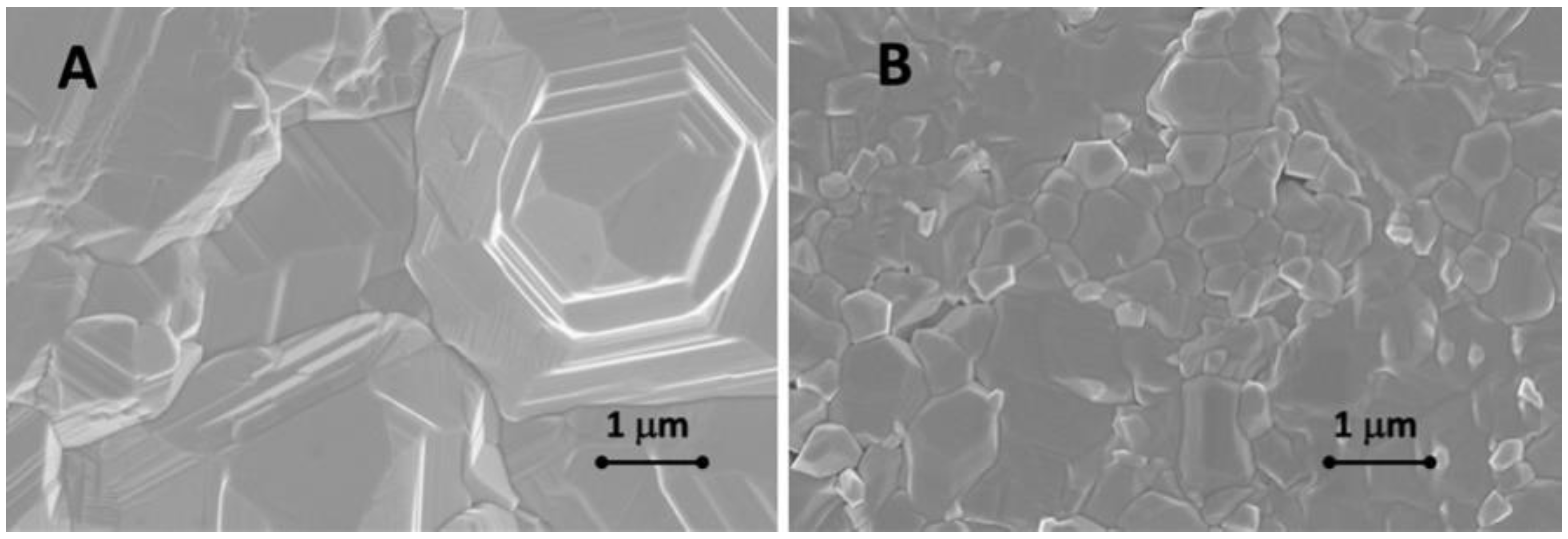
CdTe is evaporated from heated crucibles at pressures that can go from 10−5 mbar up to high vacuum evaporation of more than 10−8 mbar; the Cd and Te condensate on a heated substrate. CdTe films grow stoichiometric and with good crystal quality as far as the substrate temperature is kept above 300 °C, however it is not possible to exceed 350 °C because of re-evaporation of the material. This results in a reduced grain size and a larger amount of grain boundaries (see Figure 3). Efficiencies over 19% can be obtained with a suitable activation treatment.
2.3.2. Electro-Deposition
With this technique, both CdTe and CdS films are typically formed in aqueous solutions of CdSO4 and Te2O3 or TeO2 at temperatures around 90 °C. The Cd and Te ions are moved by potential difference on the substrate, forming CdTe with the following reaction:
Cd2+ + HTeO2+ + 3H+ + 6e → CdTe + 2H2O
The formation of CdTe is favored over the deposition of Cd alone, so when a Te atom is deposited it tends to react with Cd in 1:1 ratio, without metallic cadmium, delivering a process that is self-regulating. For this reason, it is relatively easy to form CdTe at extremely low substrate temperature (70 °C) with a very good structure.
This allows delivering a low-cost fabrication process (low temperature and atmospheric pressure) which has been carried forward by many companies, also nowadays. In the 90s BP Solar had a fabrication line with modules of up to 11% efficiency with this technique, which at that time was a record efficiency for large scale devices [43]. On a small scale the best efficiency obtained is 14.2% [44].
2.3.3. Screen Printing
This is a simple and for this reason low cost process: at atmospheric pressure a CdTe paste is mechanically laid on the substrate. The paste is prepared by crushing and blending the Cd and Te powders into an organic dispersed paste (i.e., polyene glycol in water), usually also CdCl2 is added in the paste. Subsequently the paste is mechanically spread on the substrate and later annealed at high temperatures (around 700 °C). In former times, very promising efficiencies around 11–12% were obtained by a Japanese group, however the large thickness is a strong limitation for this technology [45].
2.3.4. Metal-Organic Chemical Vapor Deposition
Also MOCVD is a technique based on precursors that are moved by carrier gases. Due to the high substrate temperature, precursors in a controlled atmosphere (up to 1 bar) react on the substrate forming the CdTe layer.
This process is more sophisticated and expensive, but at the same time it allows very precise control of the stoichiometry and of the impurities that could be incorporated. For this reason it is particularly suitable for CdTe doping, which is a very important issue for the next generation of solar cells [46].
Early works have shown the possibility of doping the absorber by incorporating As: for example Kartopu et al. have delivered a device of 13.6% efficiency with dimethylcadmium, diisopropyltellurium and trisdimethylaminoarsenic as organometallics precursors [21].
2.3.5. Sputtering
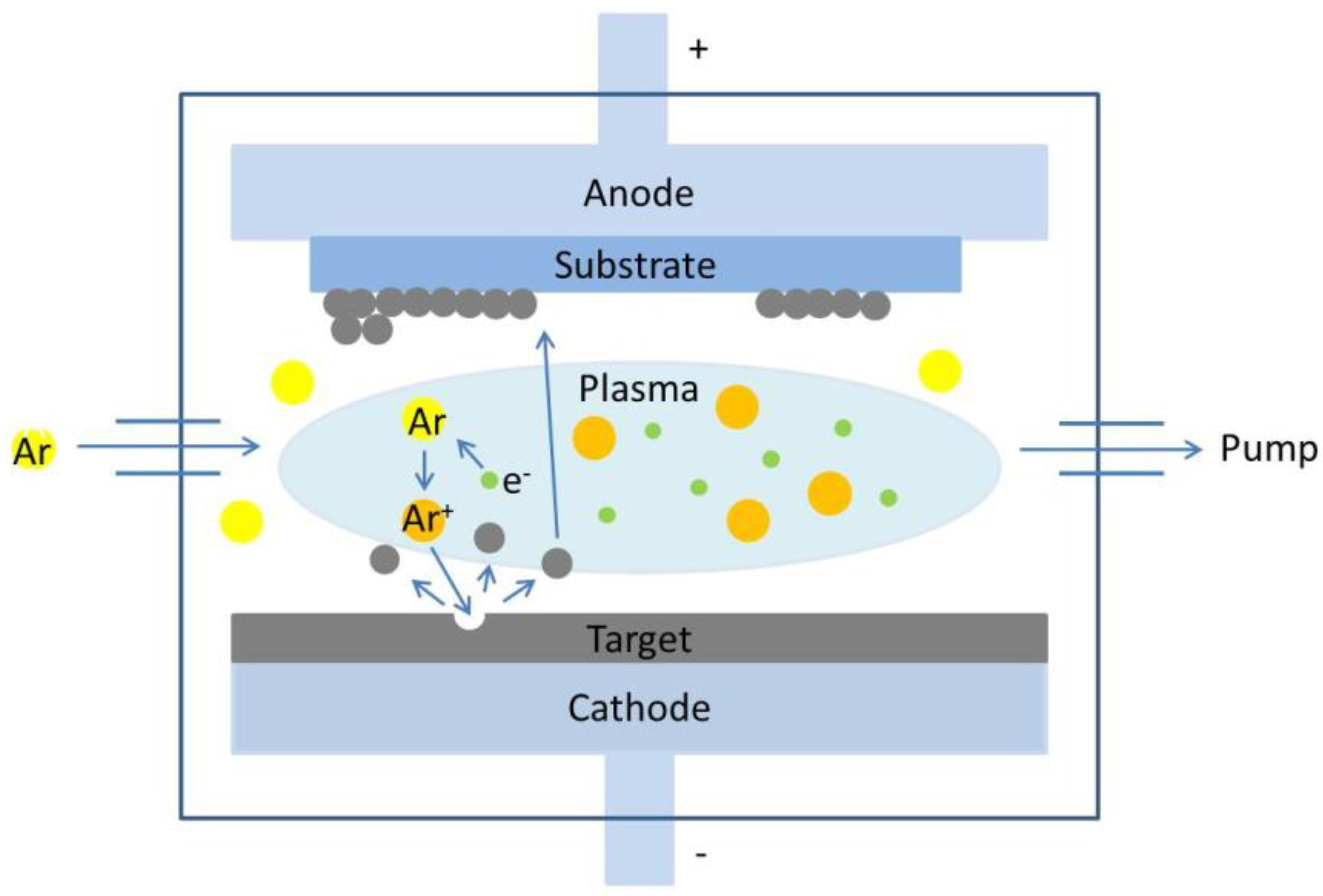
In this case, a plasma is formed by the discharge of an inert gas (i.e., Argon), then the generated ions are attracted to a target material by an electrical potential difference either in direct or in radiofrequency. The energy of the ions are transferred by collisions to the material of the target so that this is able to deposit on the substrate (see Figure 4).
In radio frequency (RF) the accelerating voltage is switching with a frequency of some kHz, while in DC is fixed. For intrinsic semiconductors and for insulators RF sputtering is necessary to avoid electrical charging on the target. DC pulsed technique is another way to avoid charging and arcing [39].
RF sputtering techniques have shown remarkable results: already in 2004 cells with 14% conversion efficiency were fabricated by optimizing the magnetron [15]. The magnetic field is designed in a way to be unbalanced, so that the field lines are not closed but completed through the side and back walls of the sputtering, this delivers 10 times higher magnetic field than the standard configuration [47].
2.3.6. Close Spaced Sublimation
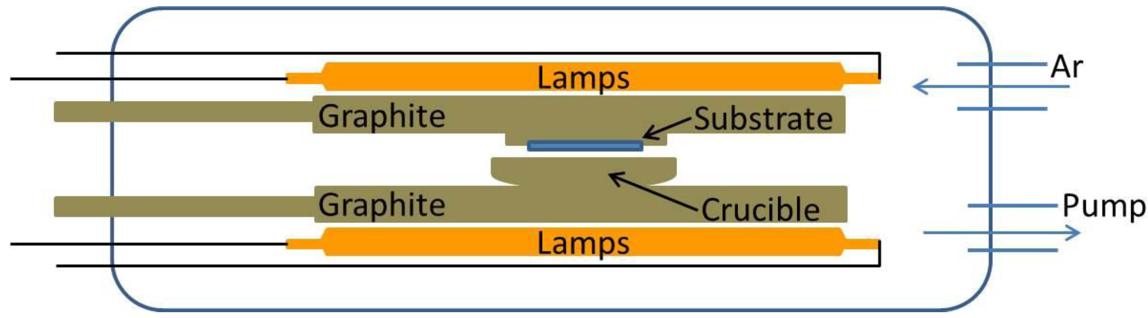
By CSS the CdTe is deposited at a pressure between 1 and 100 mbar in argon or nitrogen. The transport of the material is allowed by keeping substrate and crucible at few centimetres (see Figure 5). High pressure is useful to avoid re-evaporation of the material as the substrate temperature is kept in the range of 450 °C to 600 °C, and at the same time the high energy involved allows an excellent crystallization [48], see Figure 3.
In the crucible, CdTe splits into its single elements (2CdTe(s) ↔ 2Cd(g) + Te2(g)), these will then recombine together on the substrate.
2.3.7. Vapour Transport Deposition
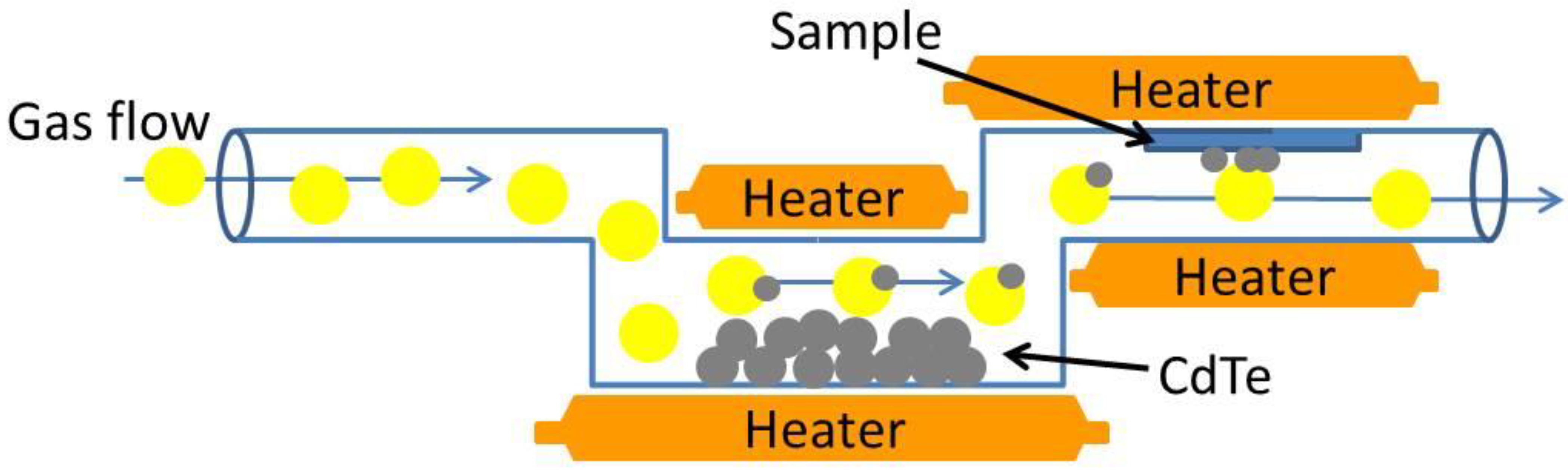
In vapour transport deposition the material is deposited at non vacuum pressures allowing high substrate temperatures like in the CSS, the main difference is that the material is carried by gases (see Figure 6).
In this way it is possible to refill the sources without interrupting the deposition line, as the sources are well away from the deposition area. This process has been introduced for industrial processes by Solar Cell Inc. (now First Solar) in collaboration with NREL [49].
The process of CdTe deposition is made of three different stages [49]:
(1) CdTe heating from a feeder and bringing it into a gas phase by a vaporizer, (2) transportation of the Cd-Te atoms in the main chamber by gas carriers through a special tube, (3) coalescence and crystal growth on the substrate.
Up to now, this process has allowed the record efficiency of 22.1% [7] obtained from a batch at the First Solar production line.
2.4. Back Contact
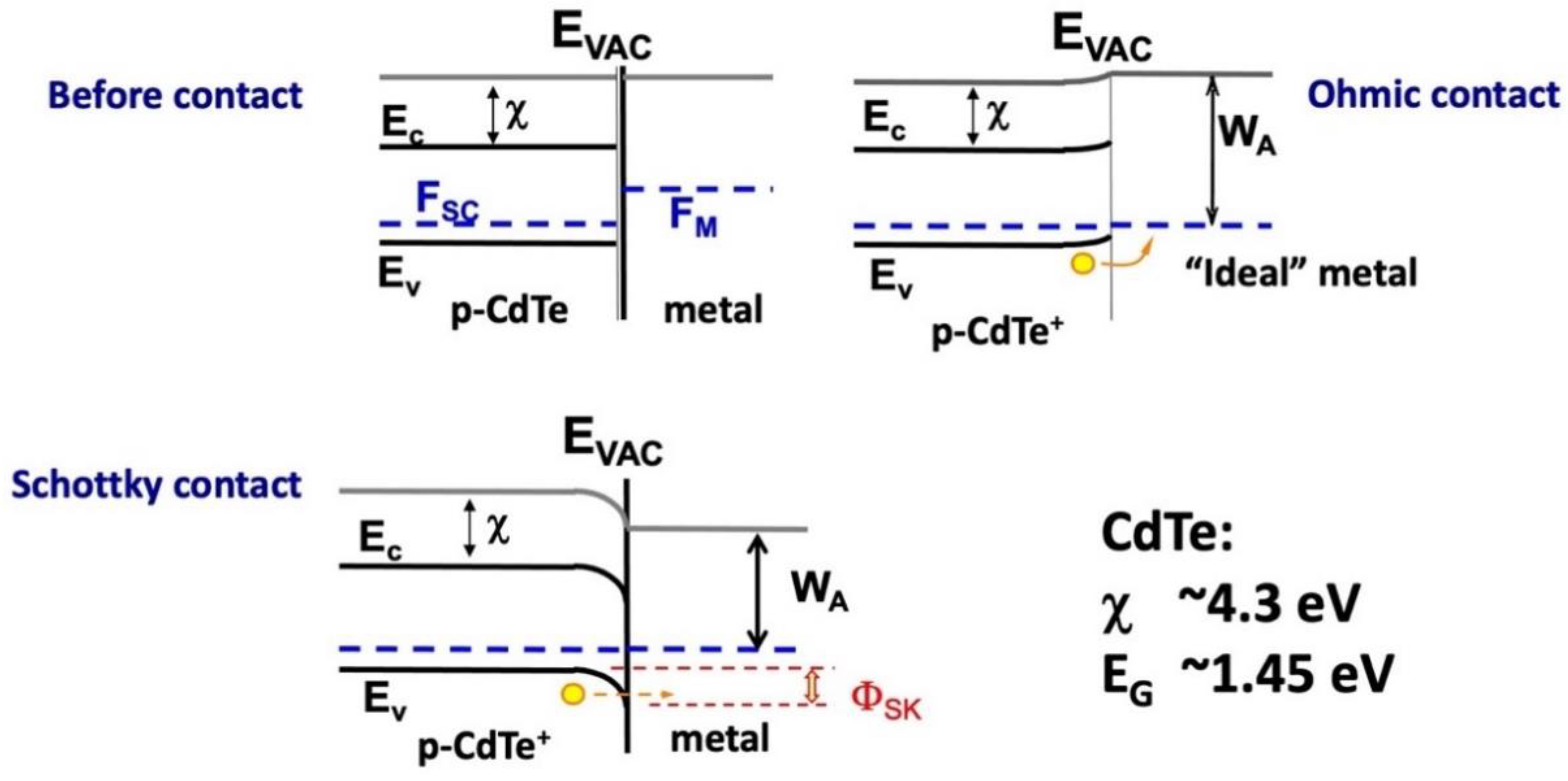
The back contact has the task of collecting the charge carriers at the absorber’s side and contact the cell with the external circuit. Usually with other technologies, as in the case of CuInGaSe2 or Cu2ZnSnSe4, a simple molybdenum layer gives a good performance, for CdTe the things are more complicated due to its high electron affinity which requires not available metals with work functions higher than 5.7 eV.
Generally, with the available metals a Schottky contact is formed, which of course presents a barrier, which can be limited if the absorber surface is highly doped [50], in this way the energy bands are curved to the metal conduction band and a so called “quasi-ohmic” contact is produced (see Figure 7).
This has been obtained by applying a Cu/metal bi-layer; in fact copper is able to increase the carrier concentration by diffusing into the first CdTe monolayers. The simplest solution is a Cu/Au bi-layer, which works very well in terms of efficiency, but provides high instability of the device due to copper diffusion. However diffusion is strictly correlated with copper amount as well as the way the CdTe surface is prepared. If a suitable CdTe etching is applied in order to generate a large quantity of Te monolayers, copper can be relatively blocked by forming CuxTe1−x [41]. This is obtained by applying either a bromine-methanol or HNO3/HPO3 mixtures.
The etching can be avoided if a sufficient amount of elemental copper is deposited on the absorber surface [41], but stability would be compromised. As a matter of fact the device would be stable only in case copper reacts with tellurium forming CuxTe, the x value needs to be lower or equal to 1.4, Cu2Te is otherwise an unstable compound able to release elemental copper in the absorber bulk [51]. Not only by etching but also by sputtering Cu1.4Te have been produced [52]. Even a very successful back contact like MoOx, which has the great advantage of having a high work function [9] is not performing very well (around 10%) without copper.
A large variety of copper combinations were developed, among them also Cu/graphite [53] or Hg and Cu-doped graphite paste. On the other hand, a different kind of back contact fabrication is to apply copper on a layer that acts as diffusion barrier, followed by a layer of molybdenum. Different successful combinations were realised with this philosophy: ZnTe:Cu [54,55,56], As2Te3:Cu, Bi2Te3:Au [57]; ZnTe is the most reliable configuration and has been widely applied.
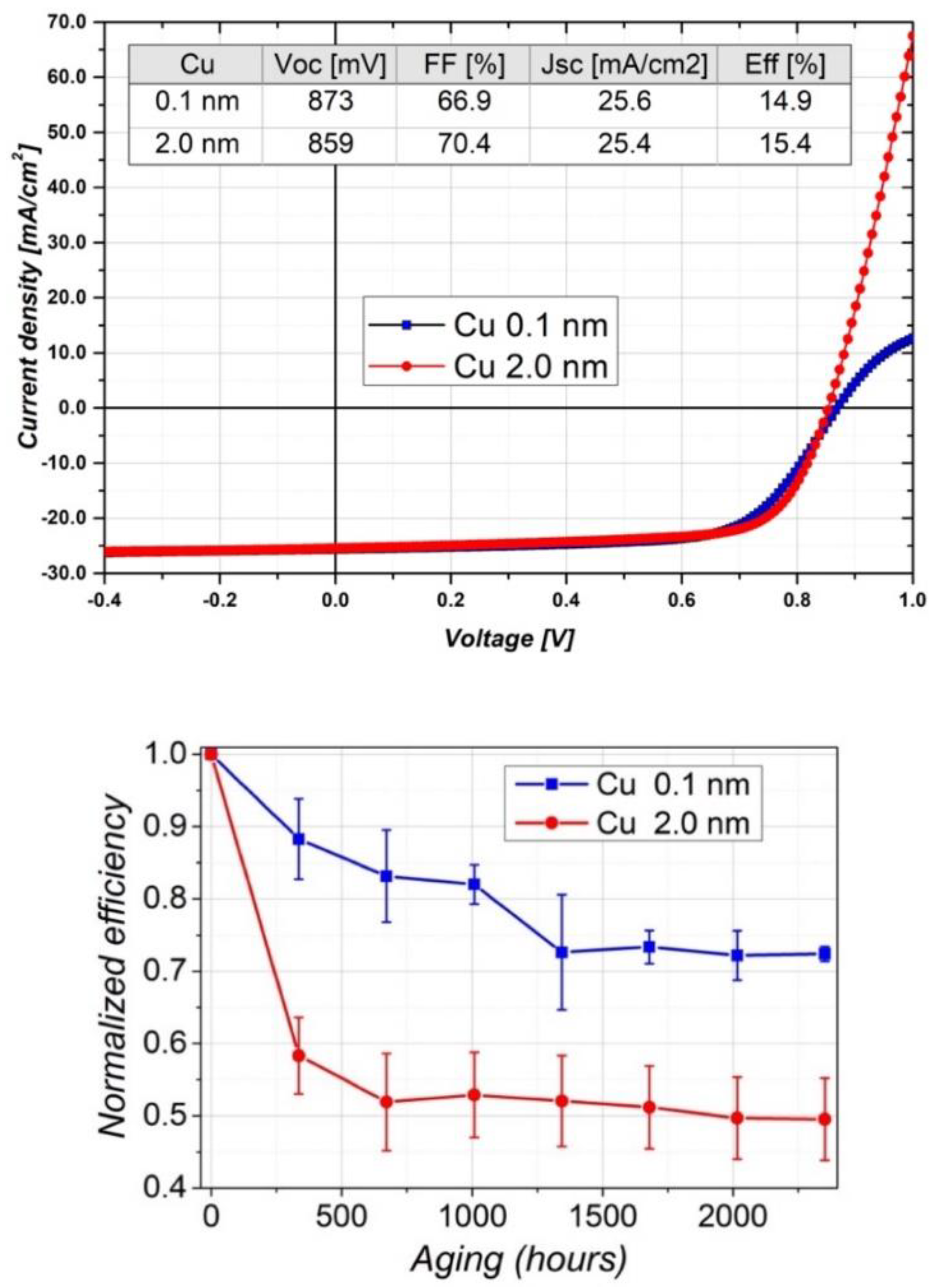
The ZnTe layer is able to limit the recombination loss of the minority carriers [58,59]. However the effectiveness of assuring the stability of the device is still depending on the copper quantity [60]. In Figure 8 (top) current-voltage characteristics, two high efficiency CdTe cells made with different amount of copper are shown. A larger amount of copper allows for a better performing back contact as clearly demonstrated by the total lack of the roll-over in the fourth quadrant. On the other hand a larger amount of copper results in a higher degradability as shown in Figure 7 (bottom).
More recently, an innovative wet deposition method is introduced by applying a solution of CuCl2 on CdTe surface. This strategy allows to insert a small optimized amount of Cu on the surface, leading to an improved stability of the devices [61].
A radical solution is, on the other hand, to avoid copper in the device. Cu-free back contacts have been introduced in the past with reasonable success, among them Ni:P, Au [62], Sb/Mo, Sb2Te3/Ni [63,64] or Sb2Te3/Mo [65]. Some of these have performed satisfying efficiency, however anytime copper is missing, solar cells perform lower efficiencies.
Figure 8.
Comparison of CdTe solar cells with minimum amount and large amount of copper: (top) current-voltage characteristics, (bottom) efficiency versus time under 80 °C and one sun illumination [63].
Figure 8.
Comparison of CdTe solar cells with minimum amount and large amount of copper: (top) current-voltage characteristics, (bottom) efficiency versus time under 80 °C and one sun illumination [63].

2.5. CdTe Activation Treatment
Post deposition treatment of CdTe is necessary to obtain high efficiencies, irrespective of the deposition method or the configuration of the solar cells. The crucial point is the effect of chlorine on the CdTe properties in a reaction at high temperature. Chlorine is delivered on CdTe in a wide variety of different ways: the most common procedure is CdCl2 deposition on CdTe and subsequent annealing (CdCl2 treatment), but in recent times other techniques such as MgCl2 or difluorochloromethane have also given very interesting results.
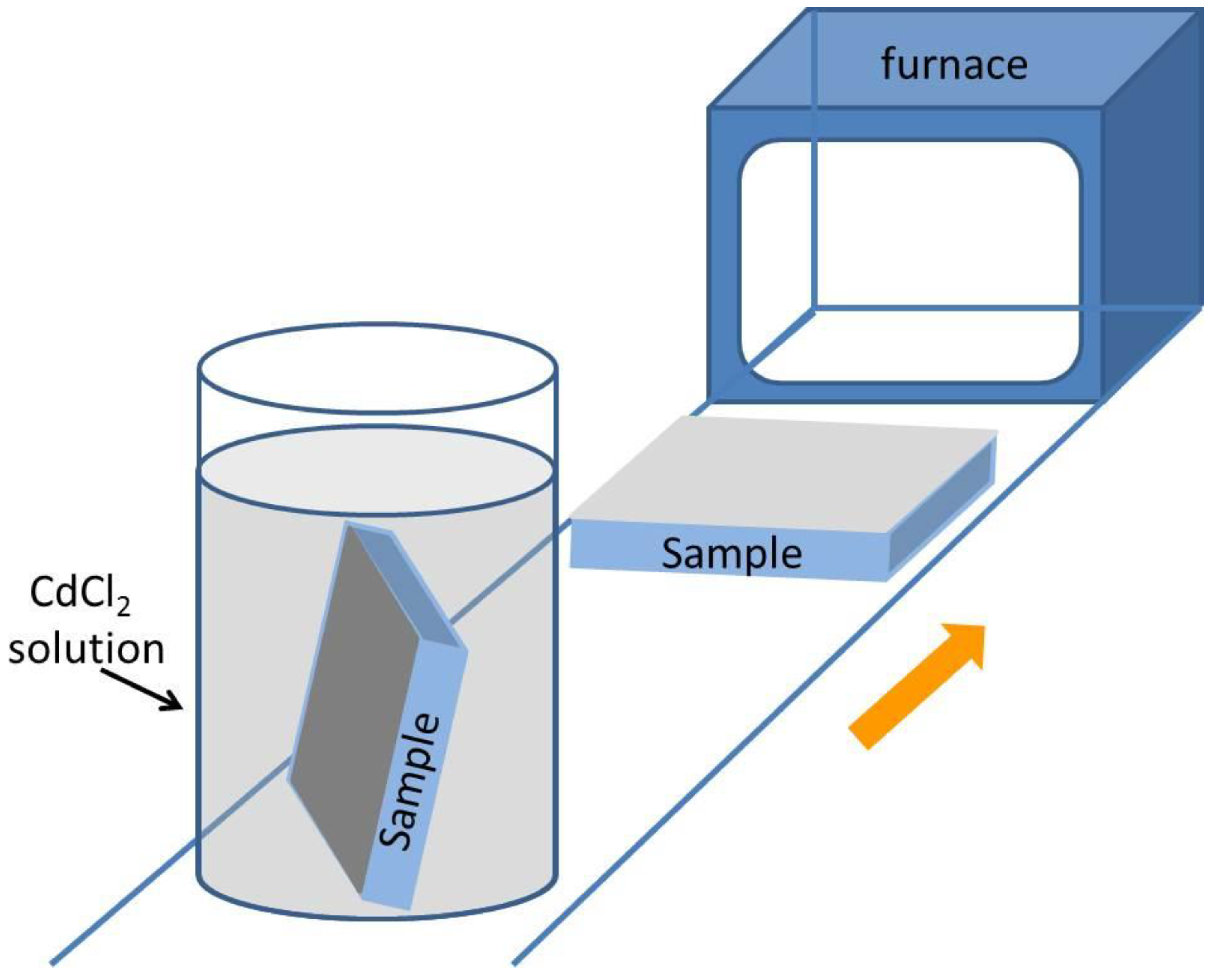
2.5.1. CdCl2 Treatment
The CdCl2 layer deposition on the CdTe is made by either physical vapour deposition or dipping in a CdCl2-methanol solution (see Figure 9). Subsequently annealing can be applied in air or in controlled atmosphere at a temperature in the range of 350–440 °C. Handling of CdCl2 is an issue at laboratory scale since it is a volatile and at the same time carcinogen material. In any case in large-scale fabrication lines wet deposition is mainly applied in order to avoid contamination and ease the cleaning of the chambers.
2.5.2. Chlorine Containing Gases
A different technology delivers Cl in the form of special gas compounds on CSS-CdTe deposited samples: in practice CdTe is heated in a chlorine containing gas atmosphere belonging to the Freon© family. The material is placed in a vacuum chamber and subsequently a mixture of argon with non-toxic chlorine containing gas (both chloro-fluorocarbons and hydro-chloro-fluorocarbons can be used) is introduced. The following reaction takes place when the system is brought at 400 °C [67]:
CdTe (s) + 2Cl2 (g)< = > CdCl2 (g) + TeCl2 (g)
This process does not need a post-treatment surface etching, because the chlorine residues are removed by evacuating the chamber after the reaction has taken place keeping the same substrate temperature. Moreover it has been demonstrated that after treatment a Te rich layer is formed on the surface [68].
2.5.3. MgCl2 Treatment
Major et al. [69] tested different chloride compounds (MgCl2, NaCl, KCl and MnCl2) as possible substitutes to CdCl2. The best results were obtained with MgCl2, comparable with the standard CdCl2 treatment, performing an efficiency of 13.5%, comparable with coeval devices fabricated with CdCl2. MgCl2 can be deposited by physical vapour deposition or by solution in methanol [69,70]. Irrespective of the way chlorine is carried on the CdTe surface, the effects of activation treatment are the followings:
2.5.4. Recrystallization
The main effect of chlorine treatment is the recrystallization of the layers. As presented before the chlorine reacts with the compound bringing this to gas form and enhancing the atom mobility.
The recrystallization of the structure is demonstrated by the change in preferred orientation of the grains, in the different shape and size and in the different structure of the grain boundaries. Cd and Te atoms reorganize so that thecrystal structure is drastically changed. The reaction, described by Mc Candless et al. [11], is the following:
CdCl2 (s) + O2 (g) + CdTe (s) < = > TeCl2 (g) + 2CdO (s)
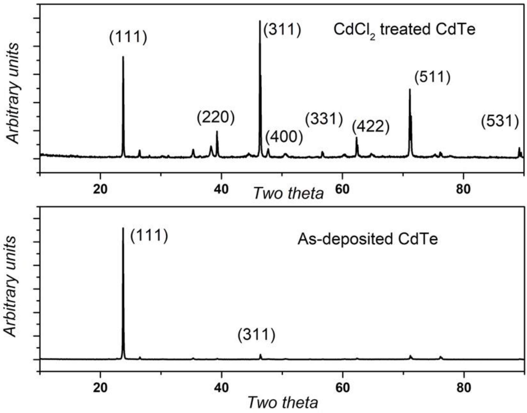
However this phenomenon is not only observed for CdTe, but also on other compounds. For example chlorine treatment on CdS enhances the grain size and changes the orientation of the grains [29,71]. In Figure 10 X-ray diffraction patterns of as-deposited and CdCl2 treated CdTe layers are shown. The (111) preferential orientation of the grains is completely lost after the activation treatment, proving that the layer has been transformed and the grains recrystallized.
The improvement of the crystallinity as a matter of fact is able to reduce the defects concentration, thus decreasing the recombination centers and limiting the loss of majority carriers [72,73].
At the same time the presence of Cl and O improves the shallow acceptors’ concentration [74,75], increased photo-carrier collection and passivation of the grain boundaries [76,77].
It has to be highlighted that chlorine itself would be a shallow donor impurity, which would compensate the intrinsic acceptors (Cd vacancies) decreasing the native p-doping of CdTe [78], however these detrimental effects are weaker than the positive ones.
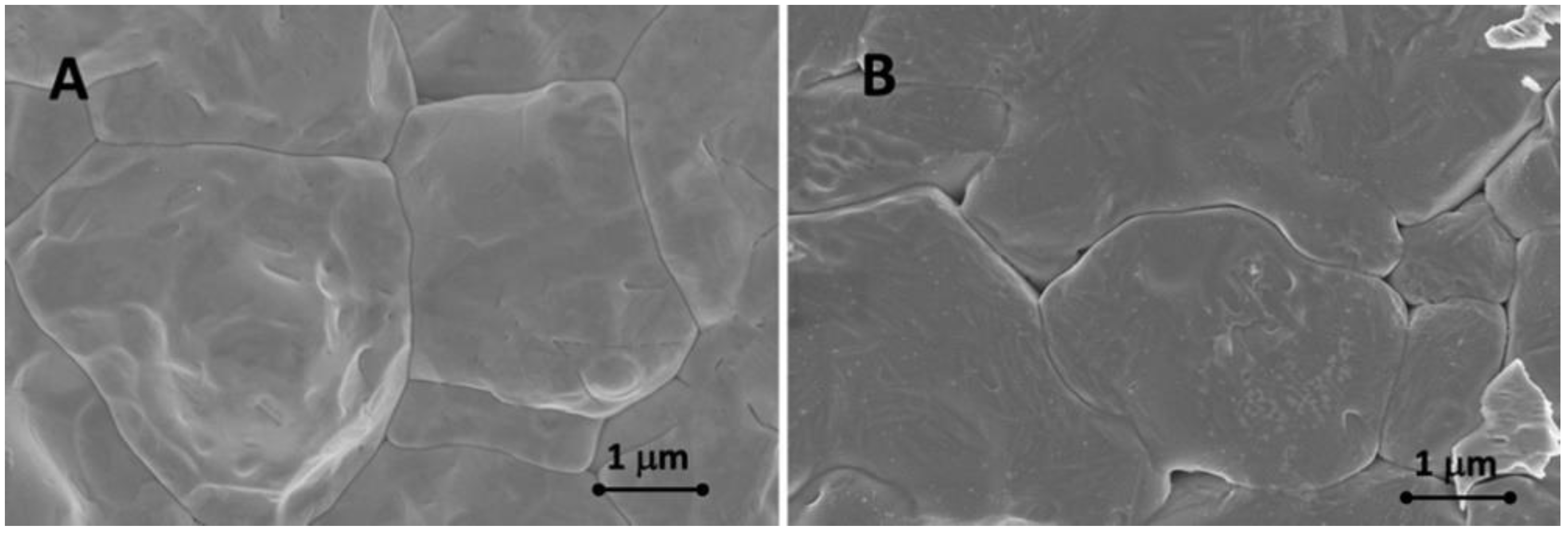
For low temperature processes recrystallization brings to grain growth. It has been observed that if CdTe is grown at a temperature in the range of 300 °C, the grain size does not exceed 1 micrometre in diameter. In this case the activation treatment (irrespective if it is applied by MgCl2, CdCl2 or Cl-containing gases) acts as a grain size enhancer with a final grain diameter size up to 5 micrometres [68,70,79], see Figure 11.
2.5.5. Intermixing
Chlorine predominantly diffuses through the grain boundaries, since its solubility in the CdTe is very limited for temperatures below 520 °C. When chlorine reaches the junction, it enhances intermixing of CdS with CdTe. This generates CdSxTe1−x layer (solid solution), which is useful for limiting stacking faults and relaxing the layers. The solid solution has a reduced lattice parameter [80,81]. It has been observed that the lattice parameter of the CdTe on CdS reduces from 6.499 to 6.446 Å when is CdCl2 treated, due to the relaxation of the compressive stress generated by the CdTe/CdS lattice mismatch [29,68]. However intermixing is stronger for low temperature deposited CdTe since in this case the layers are unstable to high temperature processes.
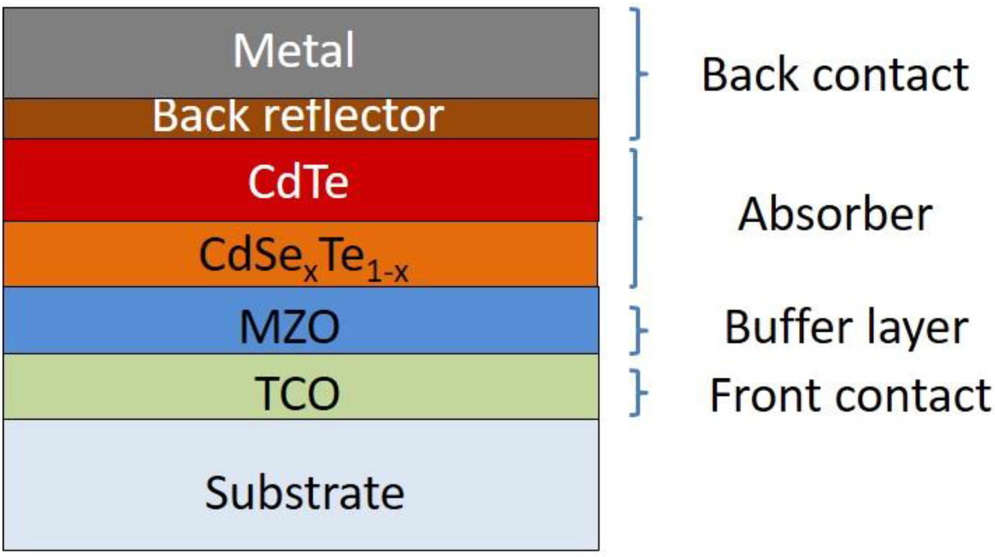
3. The New CdTe Solar Cell Structure
For a very long period, CdTe record efficiency had been kept constant at 16.7%, until recently, when conversion efficiency overcame 22%. The open circuit voltage is still well below the top values, this breakthrough depends on the large improvement of the Jsc which exceeds 30 mA/cm2 [82]. This was obtained by a specific engineering of the junction that can be divided in two very strong innovations that have revolutionised the CdTe solar cell device (see Figure 12):
- (1)
- CdSexTe1−x introduction for CdTe band gap grading
- (2)
- MgZnO introduction for high transparency
3.1. CdSexTe1−x Introduction for CdTe Band Gap Grading
Comparison of quantum efficiency measurements of solar cells fabricated with CdSe buffer between CdS and CdTe made by Paudel et al. [83] suggests that the improved current density can be attributed to a specific engineering of the junction.
The introduction of CdSe enhances the quantum efficiency response both in the blue and in the long wavelength region (825–930 nm) [83]. The mixing of the CdSe and CdTe layers by the activation treatment forms a photoactive CdSexTe1−x compound, which has a narrower band gap than pure CdTe, so that lower energy photons are also collected. The introduction of a CdSexTe1−x compound with 0.3 < x < 0.4 reduces the band gap of the absorber to approximately 1.4 eV [84]. Moreover, as shown by Wei et al., when CdS is substituted with more transparent MgZnO, improves the band alignment with CdSexTe1−x decreasing in carrier loss [84,85].
Actually, CdSe is a non-photoactive compound with a wider band gap compared to CdTe, therefore residues of it must be avoided in the finished device. Poplawsky et al. [86] proved that a CdSe layer up to 100 nm thick, deposited by sputtering, can be mixed with a subsequent CdTe layer deposited by CSS. On the other hand, a thicker CdSe layer implies residues in the finished device and consequent loss of photons in the short wavelength region. Baines et al. [87], by depositing a 100 nm thick CdSe layer by sputtering followed by CdTe by CSS, also achieved a suitable CdSexTe1−x layer, reaching a current density of 29.8 mA/cm2.
Swanson et al. prevented the residual CdSe by directly depositing a CdSexTe1−x compound by CSS prior to CdTe growth [88]. However, with this technique some optimization work was required to obtain a strong EQE gain in the long wavelength region [89]. This would suggest possible intermixing problems between CdSexTe1−x and CdTe both deposited at high temperature. Actually, with the deposition of both CdSe and CdTe layers by thermal evaporation, NREL reported the highest current density for a research institute: 31 mA/cm2, with a device efficiency of 19.2% [90]. Recently, Artegiani et al. have demonstrated that the selenization of a first thin CdTe layer is successful in favouring the mixing by activation treatment with a subsequent thicker CdTe layer, obtaining the desired CdSexTe1−x compound at the junction [91]. In Figure 11 the external quantum efficiency (electrons generated for each photons) of a device fabricated with this last mentioned process is compared with devices without CdSexTe1−x. The enahncement in response at large wavelength regions is clearly observed.
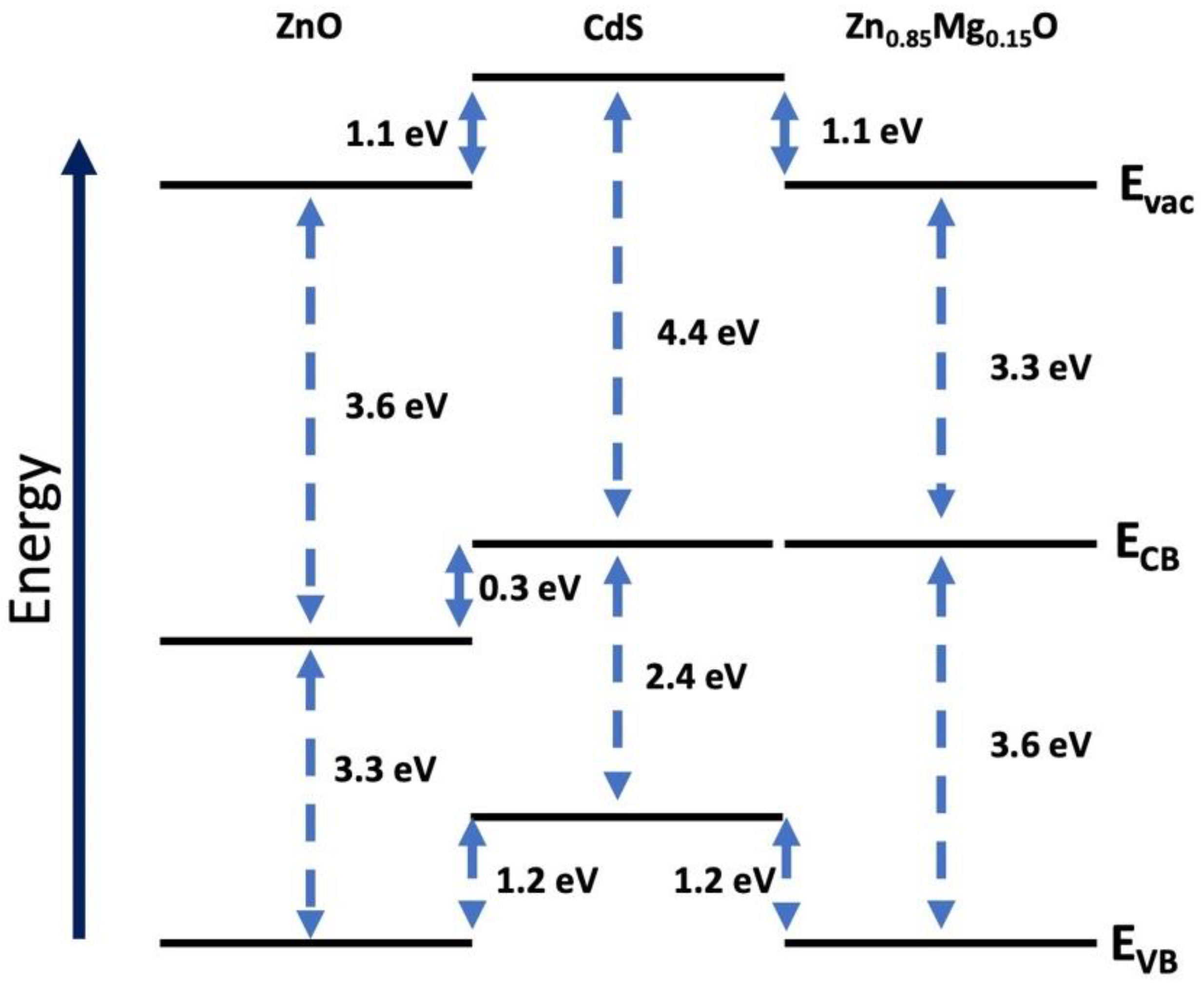
3.2. MgZnO Introduction for High Transparency
MZO improves the band alignment also with CdS [92,93], see Figure 13. MZO band gap can be tuned by the substrate temperature, controlling at the same time the Mg content. This allows to increase both current density and fill factor (FF) [92,93,94,95].
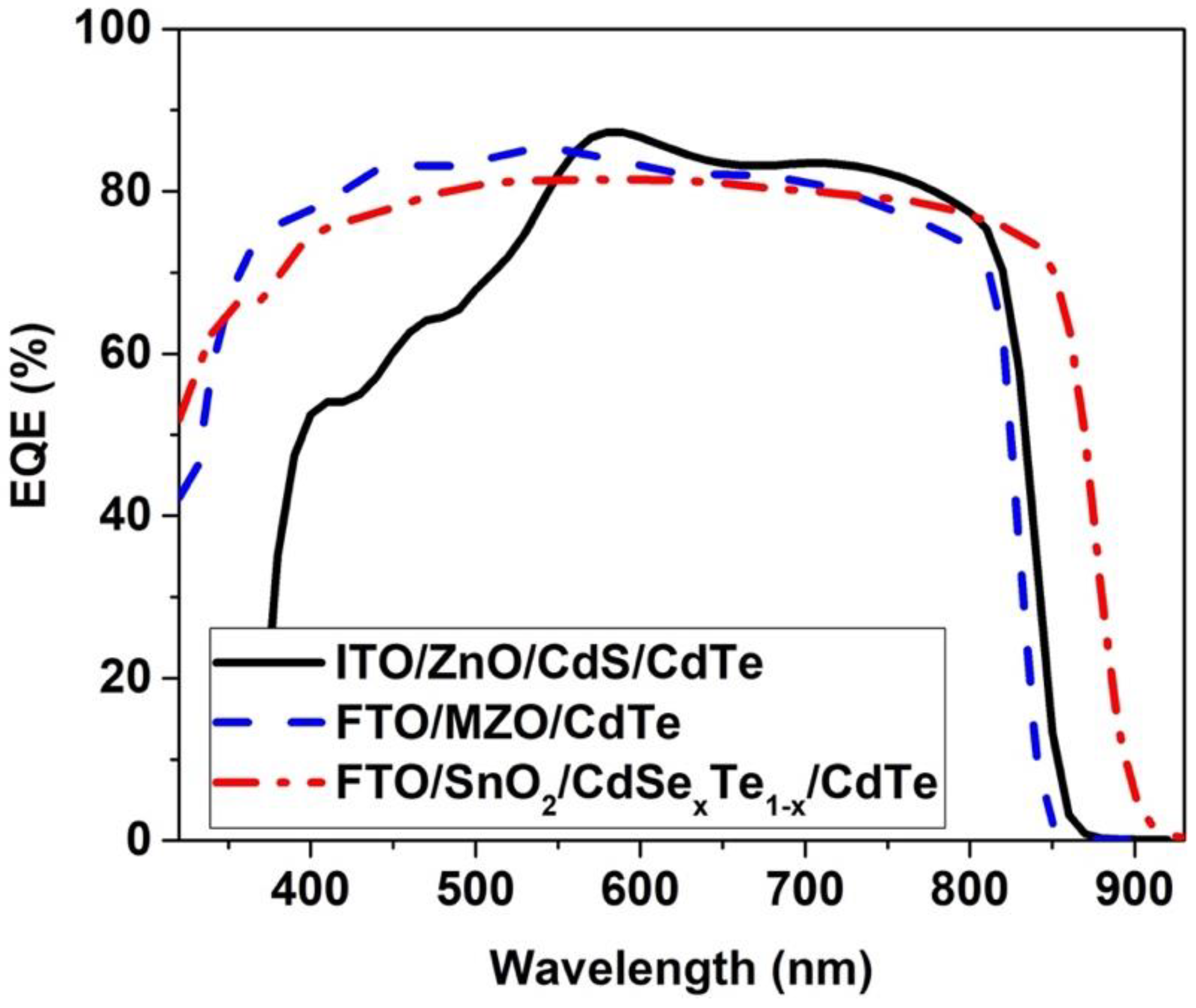
However the band gap can be tuned in order to have a very efficient alignment with CdSexTe1−x/CdTe, allowing the total removal of CdS layer from the structure and resulting in a high performing junction with no parasitic absorption in the buffer layer [96,97]. In Figure 14 the dashed blue line represents the external quantum efficiency (number of charge carriers collected divided to the number of incident photons with a specific wavelength) of MZO/CdTe junction based solar cell, the higher response in terms of transparency compared to CdS and SnO2 is clearly observed.
MZO is usually deposited either by RF sputtering of a MgxZn1−xO target, fabricated with a previously selected quantity of Mg [89,94,95,96,97], or by co-sputtering from MgO and ZnO targets [98].
Furthermore, engineering CdTe absorber by increasing the energy of the conduction band at the junction between CdTe and the back contact delivers a carriers’ back reflector. The introduction of a wider band-gap material (i.e., ZnTe, CdZnTe or CdMgTe) generates a back surface field (BSF) that reflects away from the back contact both photoelectrons and forward current electrons [99]. This increases the majority carrier lifetime and decreases the minority carrier collection [58,100,101].
4. Future Improvements and Upgrades
4.1. Increasing the Net Charge Density: Doping
One of the main limitations to high efficiency devices for CdTe based solar cells is the open circuit voltage value, which is attested -in the very best cases- in the range of 900 mV. The CdTe band gap, as previously discussed, is such that it could deliver a voltage of more than 1 V. However this does not happen, due to the relatively low carrier concentration and short lifetime.
The open-circuit voltage is the point in the current-voltage characteristic where short circuit and forward bias diffusion currents cancel each other out. The last one increases as recombination in the junction increases, reducing the open-circuit voltage.
So the open-circuit voltage is mostly depending on the reduction of carriers collection, which can depend on the recombination of the charge carriers given by the presence of minority carriers. By increasing the doping concentration, we can reduce the minority carriers’ concentration at equilibrium. On the other hand, high doping can reduce the diffusion length, and this is detrimental for the collection of the carriers.
When CdTe is grown at high substrate temperatures it usually tends to be p-doped, since Cd vacancies make the absorber p-type. However this intrinsic doping is limited and generates semiconductors with low net carrier concentration. The result is that the Voc typically does not exceed 900 mV, despite the band gap would suggest an open-circuit voltage of 1 V.
For this reason, in recent times extrinsic doping of CdTe has been one of the most challenging topics. CdTe can be doped in both p and n-type configuration; for p-type group I and V elements are used [102,103,104].
One of the main problems is that the doping elements in the polycrystals often segregate along the grain boundaries shunting the absorber. However, CdTe has been doped with alternating fortune during or after growth. Good results in the first category have been obtained with MOCVD technique, which can include doping elements in the precursors [21,105]. Other ways to deliver doped CdTe during growth are by CSS of previously doped CdTe target [106] or by in situ Sb co-evaporation in VTD technique [107]. We have already mentioned that copper deposition on top of the CdTe, or the copper/silver deposition on CdTe in substrate configuration are another successful way to dope the bulk [108]. However other techniques have been used such as the reaction of CdTe with dopant-carrier compounds in gas form [109], or MOCVD of dopant on CSS deposited CdTe [110].
Currently the most efficient devices have been obtained by doping CdTe with Cu [96], but the solubility of copper in CdTe is limited and indeed a high amount generates compensating defects [66]. Promising alternatives are other p-type dopants such as P and As. Recently Metzger et al. achieved an efficiency of 20.8% doping a CdSexTe1−x/CdTe cell with As, demonstrating a majority carrier density above 1016 cm−3 [111].
4.2. Tandem Cells
The Schottky-queisser limit puts CdTe to a record efficiency of around 32%, however this numbers will be very difficult to reach, considering the limitations of the polycrystalline junction as well as the efficiency loss for the industrial scale. An alternative way to reach very high efficiencies in a relatively short time is to combine different band gaps together in order to optimize the light absorption and energy conversion. Multijunction solar cells (made of GaAs, InGaP and other materials) reach very high efficiency but they need high costs for production and result in a non-particularly advantageous efficiency/cost ratio. Recently alternative tandem solar cells, where thin films are either matched together or with silicon crystalline, have been introduced in order to obtain high efficiency and low cost at the same time [112].
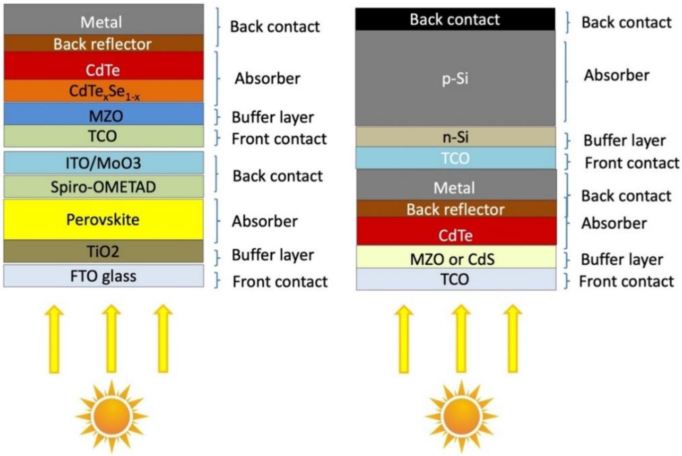
For CdTe, double junction (tandem) solar cells have been made with perovskites or with silicon as shown in Figure 15.
It is crucial, for an optimized tandem device, to align and tune the two different absorber band gaps. Perovskites are perfect in this sense since their band gap can be tuned accordingly, from 2.4 eV down to 1.5 eV, as we can change the absorber from Methylammonium lead bromide ((CH3NH3)PbBr3; MAPBr) −2.3 eV to MAPbI3 with 1.55 eV, similarly CsPbBr3 with 2.35 eV goes to 1.7 eV with CsPbI3 [113]. Calculations have shown that a tandem cell fabricated with 1.42 eV CdSexTe1−x would be ideal with a top cell where the absorber is a wide bandgap compound of 2/2.3 eV [114].
Analogously it is possible to pursue tandem devices from CdTe by applying a silicon based crystalline solar cell. In this case, silicon is the material with the lower band gap (1.1 eV) and needs to be put as bottom cell. So for this configuration a wider band gap CdTe device would be needed, and a pure CdTe absorber is possibly preferable. At the moment only calculation and simulations with AMPS-1D and SCAPS software have been made, attesting that an efficiency just below 30% can be reached with this configuration [115,116].
5. Alternative Absorbers
In recent years the research has also been concentrating on the development of new absorbers. There is no scientific necessity to actually replace CdTe, however two main issues might result from using CdTe:
- (1)
- Te scarcity
- (2)
- Perception of CdTe due to the presence of cadmium.
Questionable availability of elemental Te has been demonstrated to be a matter of concern if the production levels would overcome 20 GW per year [117]; in this case it would be necessary to go below 1.5 μm [118]. On the other hand cadmium presence as possible harmful material is very much limited problem for the reasons explained in the next section. However Cd presence has limited the investments in Europe and it can be a limitation for product integrated PV where the devices need to fulfil the Rohs directive.
Two possible alternative absorbers that have been considered are SnS and Sb2Se3. Both because of their extraordinary high absorption coefficient, their binary nature which keeps the deposition and growth of the absorber simple.
SnS thin film layers have been fabricated with a large variety of technologies: (1) physical like thermal evaporation [119] and sputtering method [120] and (2) chemical, for example spray pyrolysis method [121], Atomic layer deposition (ALD) [122,123]). A cell efficiency of 2.9% was obtained with a glass/Mo/SnS/Zn(O,S)/ZnO/ITO structure where SnS layer (450 nm) is deposited by pulsed chemical vapor deposition and Zn(O,S) buffer layer is deposited by ALD [124]. By depositing the SnS absorber via ALD the same authors achieved the 4.36% record efficiency [125]. The same group has obtained an efficiency of 3,88% by vacuum evaporation [126,127]. However the irreproducibility of the SnS growth is one of the main limitations, at the moment, to the development of SnS devices [128].
Antimony selenide (Sb2Se3) is a compound made of with abundant elements. It has interesting optoelectronic properties: a band gap of (1.1–1.2) eV, a carrier mobility of (~10 cm2 V−1 s−1 for minority carriers), absorption coefficient of (>105 cm−1 at short wavelengths) and carrier lifetime of (~60 ns). Moreover Sb2Se3 has a one-dimensional (1D) ribbon crystal structure, with covalent bonds only along the ribbon [129,130]. Antimony selenide has an evaporation temperature of 423 °C and a melting temperature of 608 °C [131].
At the moment the record efficiency for Sb2Se3 based solar cells, fabricated by VTD, is 7.6% by Wen et al. [132]. A similar high substrate temperature deposition by CSS has also shown good conversion efficiency [133]. On the other hand by vacuum evaporation the efficiency are generally lower, around 2% [131,134].
Recently the addition of sulfur element into the antimony selenide matrix, so to form Sb2(S, Se)3 which delivers a remarkable efficiency of more than 10%. Even more interesting is the fact that this result has been obtained with a non-vacuum technique [135].
6. Environmental Aspects
Despite the great success in terms of scalability of CdTe cells, the negative perception of cadmium has erroneously limited the widespread of this technology. Cadmium, in its elemental form, results to be carcinogenic and it is banned for the electrical devices that have to respond to the RoHs directive. These arguments have been used as a strong weapon against this very effective photovoltaic technology.
But the truth is a bit more complicated and the environmental impact of CdTe is actually very much different than what one might think, this has been reported and proved by a large number of studies from different laboratories [118,136,137,138,139,140,141,142]. CdTe is actually not registered as a carcinogenic compound and it results to be 100 times less toxic than elemental cadmium [141].
The difference between CdTe compound and elemental Cd was also highlighted by analysis on rats where the lethal concentration of CdTe by inhalation is 9 times higher than Cd [142]. Again, in rats no adverse reproductive effects where found [143]. So, once is clarified that CdTe is not toxic, the next question would be when and how CdTe would release elemental cadmium.
There have been analysis on the release of cadmium on cracked modules under rainwater as well as in the soil showing that its concentration was always below the concentration limits [141].
More recent studies were made in a research lab at the University of Arizona. A first study was made on CdTe meshes (63–125 µm) which showed that CdTe can partly dissolve in acetic acid, sodium hydroxide (pH ¼ 4.93 ± 0.05) (Toxicity Characteristic Leaching Procedure (TCLP) test) and in citric acid, and sodium hydroxide (pH ¼ 5.00 ± 0.05) (Waste Extraction Test, WET) [144].
However, later the same group presented a work on non-encapsulated CdTe, where 1.5 g of crushed pieces of CdTe film mixed with 300 g of crushed glass (to maintain the proportion between active material and encapsulant) are put in acidic and methanogenic column. This in order to test the possible leaching generated during the acidic phase (young landfill) and during the methanogenic phase (mature landfill). In this case a more realistic situation, since we are not dealing with micro powder, even if still a non encapsulated module was considered, so again a bit far from the real conditions. However the results showed that the Cd concentration was 6.7-times and 4.6-times below the limit defined respectively in the TCLP test and in the WET test [145].
An additional risk in releasing elemental cadmium that has to be considered is in fires. However the CdTe melting point is exceeding 1000 °C which is generally never reached in case of fires in typical residential buildings.
Only in case of fires in industrial buildings higher temperatures can be reached but it has been registered that the melting encapsulating glass was able to fix the cadmium telluride and to avoid its release in the atmosphere [139].
7. Conclusions
CdTe solar cells have shown an extraordinary efficiency improvement in recent years. This was obtained by a complete redesign of the device with the (1) development of a stable and efficient back contact that works as well as back reflector, (2) band gap tuning by introduction of CdSexTe1−x in the CdTe absorber, (3) substitution of CdS with MZO transparent buffer layer.
The final result is an efficiency of 22.1%, this value is in line with other technologies but with a higher scalability and the possibility of new BIPV structures.
These exceptional results have brought to a module installation of more than 17 GW globally [146] with efficiencies on large areas up to 19% in commercial modules. However open circuit voltage needs still additional improvement to reach the nominal value of 1000 mV, for this reason the research is now concentrating on the systematic doping of CdTe.
If a suitable doping would be obtained it is plausible to expect efficiencies in the range of 25% in the next years, with a further cut of the costs by the reduction of materials usage and optimization of the production processes.
Usually, conversion efficiencies of photovoltaic devices decrease with increasing temperatures, in particular open circuit voltage reduces consistently and short circuit current slightly improves [147]. For CdTe it has been observed that the decrease in open-circuit voltage is remarkably less than for CIGS and silicon based solar cells, resulting in 20% more overall power generation in high temperature environment [146].
Finally, a large number of scientific articles prove the extremely low environmental impact of this technology. Even non-friendly reports show that the possibility for broken modules to have high cadmium leakage in the soil is very unlikely. As well as no emission of cadmium can occur in case of residential fires. In addition, the complete recyclability of the CdTe modules makes this great technology absolutely clean.
Author Contributions
Conceptualization, A.R.; methodology, A.R.; investigation, A.R. and E.A.; resources, A.R. and E.A.; data curation, A.R.; writing—original draft preparation, A.R.; writing—review and editing, A.R. and E.A. All authors have read and agreed to the published version of the manuscript.
Funding
This research received no external funding.
Institutional Review Board Statement
Not applicable.
Informed Consent Statement
Not applicable.
Conflicts of Interest
The authors declare no conflict of interest.
References
- Bonnet, D.; Rabenhorst, H. New results on the development of a thin film p-CdTe–n-CdS heterojunction solar cell. In Proceedings of the 9th Photovoltaic Specialists Conference, Silver Spring, MD, USA, 1972; pp. 129–131. [Google Scholar]
- Leading Solar PV Manufacturers Based on Module Shipments in 2018 and 2019. Available online: https://www.statista.com/statistics/858456/global-companies-for-pv-cell-and-module-shipments/ (accessed on 21 January 2021).
- Rühle, S. Tabulated values of the Shockley-Queisser limit for single junction solar cells. Sol. Energy 2016, 130, 139–147. [Google Scholar] [CrossRef]
- Britt, J.; Ferekides, C.S. Thin-film CdS/CdTe solar cell with 15.8% efficiency. Appl. Phys. Lett. 1993, 62, 2851–2852. [Google Scholar] [CrossRef]
- Wu, X.; Dhere, R.G.; Albin, D.S.; Gessert, T.A.; Dehart, C.; Keane, J.C.; Duda, A.; Coutts, T.J.; Asher, S.; Levi, D.H.; et al. High-Efficiency CTO/ZTO/CdS CdTe Polycrystalline Thin-Film Solar Cells. In Proceedings of the NCPV Program Review Meeting, Lakewood, CO, USA, 14–17 October 2001. [Google Scholar]
- First Solar Record 21.5 Percent Conversion Efficiency Research Cell Validates Technology Roadmap. 2015. Available online: https://www.sonnenseite.com/en/energy/first-solar-record-21-5-percent-conversion-efficiency-research-cell-validates-technology-roadmap/ (accessed on 21 January 2021).
- Green, M.A.; Dunlop, E.D.; Hohl-Ebinger, J.; Yoshita, M.; Kopidakis, N.; Hao, X. Solar cell efficiency tables (version 56). Prog. Photovolt. Res. Appl. 2020, 28, 629–638. [Google Scholar] [CrossRef]
- Mathew, X.; Enriquez, J.P.; Romeo, A.; Tiwari, A.N. CdTe/CdS solar cells on flexible substrates. Sol. Energy 2004, 77, 831–838. [Google Scholar] [CrossRef]
- Kranz, L.; Gretener, C.; Perrenoud, J.; Schmitt, R.; Pianezzi, F.; La Mattina, F.; Blösch, P.; Cheah, E.; Chirilă, A.; Fella, C.M.; et al. Doping of polycrystalline CdTe for high-efficiency solar cells on flexible metal foil. Nat. Commun. 2013, 4, 1–7. [Google Scholar] [CrossRef] [Green Version]
- Salavei, A.; Menossi, D.; Piccinelli, F.; Kumar, A.; Mariotto, G.; Barbato, M.; Meneghini, M.; Meneghesso, G.; Di Mare, S.; Artegiani, E.; et al. Comparison of high efficiency flexible CdTe solar cells on different substrates at low temperature deposition. Sol. Energy 2016, 139, 13–18. [Google Scholar] [CrossRef]
- McCandless, B.E.; Dobson, K.D. Processing options for CdTe thin film solar cells. Sol. Energy 2004, 77, 839–856. [Google Scholar] [CrossRef]
- Artegiani, E.; Menossi, D.; Salavei, A.; di Mare, S.; Romeo, A. Analysis of the influence on the performance degradation of CdTe solar cells by the front contact. Thin Solid Films 2017, 633, 101–105. [Google Scholar] [CrossRef]
- Alamri, S.N.; Brinkman, A.W. The effect of the transparent conductive oxide on the performance of thin film CdS/CdTe solar cells. J. Phys. D Appl. Phys. 2000, 33, L1–L4. [Google Scholar] [CrossRef]
- Romeo, N.; Bosio, A.; Canevari, V.; Terheggen, M.; Vaillant Roca, L. Comparison of different conducting oxides as substrates for CdS/CdTe thin film solar cells. Thin Solid Films 2003, 431–432, 364–368. [Google Scholar] [CrossRef]
- Gupta, A.; Compaan, A.D. All-sputtered 14% CdS∕CdTeCdS∕CdTe thin-film solar cell with ZnO:Al transparent conducting oxide. Appl. Phys. Lett. 2004, 85, 684–686. [Google Scholar] [CrossRef]
- Perrenoud, J.; Kranz, L.; Buecheler, S.; Pianezzi, F.; Tiwari, A.N. The use of aluminium doped ZnO as transparent conductive oxide for CdS/CdTe solar cells. Thin Solid Films 2011, 519, 7444–7448. [Google Scholar] [CrossRef]
- Purica, M.; Budianu, E.; Rusu, E.; Danila, M.; Gavrila, R. Optical and structural investigation of ZnO thin films prepared by chemical vapor deposition (CVD). Thin Solid Films 2002, 403–404, 485–488. [Google Scholar] [CrossRef]
- Ennaoui, A.; Weber, M.; Scheer, R.; Lewerenz, H.J. Chemical-bath ZnO buffer layer for CuInS2 thin-film solar cells. Sol. Energy Mater. Sol. Cells 1998, 54, 277–286. [Google Scholar] [CrossRef]
- Maruyama, T.; Tabata, K. Fluorine-doped tin dioxide thin films prepared by chemical vapor deposition. J. Appl. Phys. 1990, 68, 4282–4285. [Google Scholar] [CrossRef] [Green Version]
- Wu, X.; Sheldon, P.; Coutts, T.J.; Rose, D.H.; Moutinho, H.R. Application of Cd2SnO4 transparent conducting oxides CdS/CdTe thin-film devices. In Proceedings of the 26th IEEE Photovoltaic Specialists Conference, Anaheim, CA, USA, 29 September–3 October 1997; pp. 347–350. [Google Scholar]
- Kartopu, G.; Clayton, A.J.; Brooks, W.S.M.; Hodgson, S.D.; Barrioz, V.; Maertens, A.; Lamb, D.A.; Irvine, S.J.C. Effect of window layer composition in Cd1_xZnxS/CdTe solar cells. Prog. Photovolt. Res. Appl. 2014, 22, 18–23. [Google Scholar] [CrossRef]
- Wu, X.; Keane, J.C.; Dhere, R.G.; DeHart, C.; Duda, A.; Gessert, T.A.; Asher, S.; Levi, D.H.; Sheldon, P. 16.5%-efficient CdS/CdTe polycrystalline thin-film solar cell. In Proceedings of the 17th European Photovoltaic Solar Energy Conference, Munich, Germany, 22–26 October 2001; pp. 995–1000. [Google Scholar]
- Ferekides, C.S.; Marinskiy, D.; Viswanathan, V.; Tetali, B.; Palekis, V.; Selvaraj, P.; Morel, D.L.; Telali, B.; Palekis, V.; Selvaraj, P.; et al. High efficiency CSS CdTe solar cells. Thin Solid Films 2000, 361–362, 520–526. [Google Scholar] [CrossRef]
- Romeo, N.; Bosio, A.; Romeo, A. An innovative process suitable to produce high-efficiency CdTe/CdS thin-film modules. Sol. Energy Mater. Sol. Cells 2010, 94, 2–7. [Google Scholar] [CrossRef]
- Boyle, D.S.; Bayer, A.; Heinrich, M.R.; Robbe, O.; O’Brien, P. Novel approach to the chemical bath deposition of chalcogenide semiconductors. Thin Solid Films 2000, 361. [Google Scholar] [CrossRef]
- Sandoval-Paz, M.G.; Sotelo-Lerma, M.; Mendoza-Galvan, A.; Ramírez-Bon, R. Optical properties and layer microstructure of CdS films obtained from an ammonia-free chemical bath deposition process. Thin Solid Films 2007, 515. [Google Scholar] [CrossRef]
- Zhang, H.; Ma, X.; Yang, D. Effects of complexing agent on CdS thin films prepared by chemical bath deposition. Mater. Lett. 2004, 58. [Google Scholar] [CrossRef]
- Romeo, A.; Baetzner, D.L.; Zogg, H.; Tiwari, A.N.; Vignali, C. Influence of CdS growth process on the structural and photovoltaic properties of CdTe/ CdS solar cells. Sol. Energy Mater. Sol. Cells 2001, 67, 311–321. [Google Scholar] [CrossRef]
- Romeo, A.; Baetzner, D.L.; Zogg, H.; Tiwari, A.N. Recrystallization in CdTe/CdS. Thin Solid Films 2000, 361–362, 420–425. [Google Scholar] [CrossRef] [Green Version]
- Skarp, J.; Koskinen, Y.; Lindfors, S.; Rautiainen, A.; Suntola, T. Development and Evaluation of Cds/CdTe Thin Film PV Cells. In Tenth E.C. Photovoltaic Solar Energy Conference, Proceedings of the International Conference, Lisbon, Portugal, 8–12 April 1991; Luque, A., Sala, G., Palz, W., Dos Santos, G., Helm, P., Eds.; Springer: Dordrecht, The Netherlands, 1991; pp. 567–569. ISBN 978-94-011-3622-8. [Google Scholar]
- Skarp, J.; Anttila, E.; Rautiainen, A.; Suntola, T. ALE-CdS/CdTe-PV-CELLS. Int. J. Sol. Energy 1992, 12, 137–142. [Google Scholar] [CrossRef]
- Das, S.K.; Morris, G.C. Influence of growth and microstructure of electrodeposited cadmium telluride films on the properties of n-CdS/p-CdTe thin-film solar cells. J. Appl. Phys. 1992, 72, 4940–4945. [Google Scholar] [CrossRef] [Green Version]
- Morris, G.C.; Das, S. Some fabrication procedures for electrodeposited CdTe solar cells. Int. J. Sol. Energy 1992, 12, 95–108. [Google Scholar] [CrossRef]
- Ikegami, S. CdS/CdTe solar cells by the screen-printing-sintering technique: Fabrication, photovoltaic properties and applications. Sol. Cells 1988, 23, 89–105. [Google Scholar] [CrossRef]
- Matsumoto, H.; Kuribayashi, K.; Uda, H.; Komatsu, Y.; Nakano, A.; Ikegami, S. Screen-printed CdS/CdTe solar cell of 12.8% efficiency for an active area of 0.78 cm2. Sol. Cells 1984, 11, 367–373. [Google Scholar] [CrossRef]
- Zoppi, G.; Durose, K.; Irvine, S.J.C.; Barrioz, V. Grain and crystal texture properties of absorber layers in MOCVD-grown CdTe/CdS solar cells. Semicond. Sci. Technol. 2006, 21, 763–770. [Google Scholar] [CrossRef]
- Bonnet, D. THE CdTe Thin Film Solar Cell—An Overview. Int. J. Sol. Energy 1992, 12, 1–14. [Google Scholar] [CrossRef]
- Swanson, D.E.; Kephart, J.M.; Kobyakov, P.S.; Walters, K.; Cameron, K.C.; Barth, K.L.; Sampath, W.S.; Drayton, J.; Sites, J.R. Single vacuum chamber with multiple close space sublimation sources to fabricate CdTe solar cells. J. Vac. Sci. Technol. A 2016, 34, 21202. [Google Scholar] [CrossRef]
- Lisco, F. High Rate Deposition Processes for Thin Film Cdte Solar Cells; Loughborough University: Loughborough, UK, 2015. [Google Scholar]
- Kephart, J.M.; Geisthardt, R.M.; Sampath, W.S. Optimization of CdTe thin-film solar cell efficiency using a sputtered, oxygenated CdS window layer. Prog. Photovolt. Res. Appl. 2015, 23, 1484–1492. [Google Scholar] [CrossRef]
- Rimmaudo, I.; Salavei, A.; Artegiani, E.; Menossi, D.; Giarola, M.; Mariotto, G.; Gasparotto, A.; Romeo, A. Improved stability of CdTe solar cells by absorber surface etching. Sol. Energy Mater. Sol. Cells 2017, 162. [Google Scholar] [CrossRef]
- Gretener, C.; Perrenoud, J.; Kranz, L.; Kneer, L.; Schmitt, R.; Buecheler, S.; Tiwari, A.N. CdTe/CdS thin film solar cells grown in substrate configuration. Prog. Photovolt. Res. Appl. 2013, 21, 1580–1586. [Google Scholar] [CrossRef]
- Cunningham, D.W.; Skinner, D.E. Apollo ® Thin Film Process Development: Final Technical Report, April 1998—April 2002; US Department of Energy: Washington, DC, USA, 2002.
- Woodcock, J.M.; Turner, A.K.; Oszsan, M.E.; Summers, J.G. Thin film solar cells based on electrodeposited CdTe. In Proceedings of the 22nd IEEE Photovoltaic Specialists Conference, Las Vegas, NV, USA, 7–11 October 1991; p. 842. [Google Scholar]
- Nakayama, N.; Matsumoto, H.; Nakano, A.; Ikegami, S.; Uda, H.; Yamashita, T. Screen Printed Thin Film {CdS}/{CdTe} Solar Cell. Jpn. J. Appl. Phys. 1980, 19, 703–712. [Google Scholar] [CrossRef]
- Kartopu, G.; Phillips, L.J.; Barrioz, V.; Irvine, S.J.C.; Hodgson, S.D.; Tejedor, E.; Dupin, D.; Clayton, A.J.; Rugen-Hankey, S.L.; Durose, K. Progression of metalorganic chemical vapour-deposited CdTe thin-film PV devices towards modules. Prog. Photovolt. Res. Appl. 2016, 24, 283–291. [Google Scholar] [CrossRef]
- Shao, M.; Fischer, A.; Grecu, D.; Jayamaha, U.N.; Bykov, E.; Contreras-Puente, G.; Bohn, R.G.; Compaan, A.D. Radio-frequency-magnetron-sputtered CdS/CdTe solar cells on soda-lime glass. Appl. Phys. Lett. 1996, 69, 3045–3047. [Google Scholar] [CrossRef]
- Bonnet, D.; Henrichs, B.; Richter, H. High rate deposition of high quality CdTe films for high efficiency solar cell. In Proceedings of the Twenty Second IEEE Photovoltaic Specialists Conference, Las Vegas, NV, USA, 7–11 October 1991; pp. 1165–1168. [Google Scholar]
- Powell, R.C.; Dorer, G.L.; Jayamaha, U.; Hanak, J.J. Technology Support for Initiation of High-Throughput Processing of Thin Film CdTe PV: Phase 3 Final Technical Report, 14 March 1997–1 April 1998; US Department of Energy: Washington, DC, USA, 1998.
- Ferekides, C.S.; Viswanathan, V.; Morel, D.L. RF sputtered back contacts for CdTe/CdS thin film solar cells. In Proceedings of the 26th IEEE Photovoltaic Specialists Conference, Anaheim, CA, USA, 29 September–3 October 1997; pp. 423–426. [Google Scholar]
- Wu, X.; Zhou, J.; Duda, A.; Yan, Y.; Teeter, G.; Asher, S.; Metzger, W.K.; Demtsu, S.; Wei, S.-H.; Noufi, R. Phase control of CuxTe film and its effects on CdS/CdTe solar cell. Thin Solid Films 2007, 515, 5798–5803. [Google Scholar] [CrossRef]
- Nawarange, A.W.; Compaan, A.D. Optimization of Back Contacts for CdTe Solar Cells using sputtered CuxTe. In Proceedings of the 37th IEEE Photovoltaic Specialists Conference, Seattle, WA, USA, 19–24 June 2011; pp. 1317–1321. [Google Scholar]
- Suyama, N.; Arita, T.; Nishiyama, Y.; Ueno, N.; Kitamura, S.; Murozono, M. CdS/CdTe solar cells by the screen-printing sintering technique. In Proceedings of the 21th IEEE Photovoltaic Specialists Conference, Kissimmee, FL, USA, 21–25 May 1990; pp. 498–503. [Google Scholar]
- Gessert, T.A.; Mason, A.R.; Sheldon, P.; Swartzlander, A.B.; Niles, D.; Coutts, T.J. Development of Cu-doped ZnTe as a back-contact interface layer for thin-film CdS/CdTe solar cells. J. Vac. Sci. Technol. A Vac. Surfaces Film. 1996, 14, 806–812. [Google Scholar] [CrossRef]
- Mondal, A.; McCandless, B.E.; Birkmire, R.W. Electrochemical deposition of thin ZnTe films as a contact for CdTe solar cells. Sol. Energy Mater. Sol. Cells 1992, 26, 181–187. [Google Scholar] [CrossRef]
- Li, J.V.; Duenow, J.N.; Kuciauskas, D.; Kanevce, A.; Dhere, R.G.; Young, M.R.; Levi, D.H. Electrical Characterization of Cu Composition Effects in CdS / CdTe Thin-Film Solar Cells with a ZnTe: Cu Back Contact Preprint. IEEE J. Photovolt. 2013, 3, 1095–1099. [Google Scholar] [CrossRef]
- Romeo, A.; Salavei, A.; Rimmaudo, I.; Bosio, A.; Menossi, D.; Piccinelli, F.; Romeo, N. Electrical Characterization and Aging of CdTe Thin Film Solar Cells with Bi 2 Te 3 Back Contact. In Proceedings of the IEEE 39th Photovoltaic Specialists Conference (PVSC), Tampa, FL, USA, 16–21 June 2013; pp. 1178–1182. [Google Scholar]
- Amin, N.; Sopian, K.; Konagai, M. Numerical modeling of CdS/CdTe and CdS/CdTe/ZnTe solar cells as a function of CdTe thickness. Sol. Energy Mater. Sol. Cells 2007, 91, 1202–1208. [Google Scholar] [CrossRef]
- Sites, J.; Pan, J. Strategies to increase CdTe solar-cell voltage. Thin Solid Films 2007, 515, 6099–6102. [Google Scholar] [CrossRef]
- Tang, J.; Mao, D.; Ohno, T.R.; Kaydanov, V.; Trefny, J.U. Properties of ZnTe:Cu thin films and CdS/CdTe/ZnTe solar cells. In Proceedings of the 26th IEEE Photovoltaic Specialists Conference, Anaheim, CA, USA, 29 September–3 October 1997; pp. 439–442. [Google Scholar]
- Artegiani, E.; Major, J.D.; Shiel, H.; Dhanak, V.; Ferrari, C.; Romeo, A. How the amount of copper influences the formation and stability of defects in CdTe solar cells. Sol. Energy Mater. Sol. Cells 2020, 204, 110228. [Google Scholar] [CrossRef]
- Artegiani, E.; Menossi, D.; Shiel, H.; Dhanak, V.; Major, J.D.; Gasparotto, A.; Sun, K.; Romeo, A. Analysis of a novel CuCl 2 back contact process for improved stability in CdTe solar cells. Prog. Photovolt. Res. Appl. 2019, 27, 706–715. [Google Scholar] [CrossRef]
- Niemegeers, A.; Burgelman, M. Effects of the Au/CdTe back contact on IV and CV characteristics of Au/CdTe/CdS/TCO solar cells. J. Appl. Phys. 1997, 81, 2881. [Google Scholar] [CrossRef]
- Abken, A.E.; Bartelt, O.J. Sputtered Mo/Sb2Te3 and Ni/Sb2Te3 layers as back contacts for CdTe/CdS solar cells. Thin Solid Films 2002, 403–404, 216–222. [Google Scholar] [CrossRef]
- Bätzner, D.L.; Romeo, A.; Zogg, H.; Wendt, R.; Tiwari, A.N. Development of efficient and stable back contacts on CdTe/CdS solar cells. Thin Solid Films 2001, 387, 151–154. [Google Scholar] [CrossRef]
- Romeo, N.; Bosio, A.; Tedeschi, R.; Romeo, A.; Canevari, V. A highly efficient and stable CdTe/CdS thin film solar cell. Sol. Energy Mater. Sol. Cells 1999, 58, 209–218. [Google Scholar] [CrossRef]
- Romeo, N.; Bosio, A.; Romeo, A.; Mazzamuto, S.; Canevari, V. High Efficiency CdTe/CdS Thin Film Solar Cells Prepared by Treating CdTe Films with a Freon Gas in Substitution of CdCl2. In Proceedings of the 21st European Photovoltaic Solar Energy Conference, Dresden, Germany, 4–8 September 2006; p. 1857. [Google Scholar]
- Salavei, A.; Rimmaudo, I.; Piccinelli, F.; Zabierowski, P.; Romeo, A. Study of difluorochloromethane activation treatment on low substrate temperature deposited CdTe solar cells. Sol. Energy Mater. Sol. Cells 2013, 112, 190–195. [Google Scholar] [CrossRef]
- Major, J.D.; Treharne, R.E.; Phillips, L.J.; Durose, K. A low-cost non-toxic post-growth activation step for CdTe solar cells. Nature 2014, 511, 334–337. [Google Scholar] [CrossRef]
- Menossi, D.; Artegiani, E.; Salavei, A.; Di Mare, S.; Romeo, A. Study of MgCl 2 activation treatment on the defects of CdTe solar cells by capacitance-voltage, drive level capacitance profiling and admittance spectroscopy techniques. Thin Solid Films 2017, 633, 97–100. [Google Scholar] [CrossRef]
- Leoncini, M.; Artegiani, E.; Lozzi, L.; Barbato, M.; Meneghini, M.; Meneghesso, G.; Cavallini, M.; Romeo, A. Difluorochloromethane treated thin CdS buffer layers for improved CdTe solar cells. Thin Solid Films 2019, 672, 7–13. [Google Scholar] [CrossRef]
- Consonni, V.; Feuillet, G.; Renet, S. Spectroscopic analysis of defects in chlorine doped polycrystalline CdTe. J. Appl. Phys. 2006, 99, 53502–53507. [Google Scholar] [CrossRef]
- Stadler, W.; Hofmann, D.M.; Meyer, B.K.; Krause-Rehberg, B.; Polity, A.; Abgarjan, T.; Salk, M.; Benz, K.W.; Azoulay, M. Compensation Models in Chlorine dopoed CdTe based on positron annhilation and photoluminescence spectroscopy. Acta Phys. Pol. Ser. A 1995, 88, 921–924. [Google Scholar] [CrossRef]
- Tyan, Y.-S.; Vazan, F.; Barge, T.S. Effect of oxygen on thin-film CdS/CdTe solar cells. In Proceedings of the Conference records of 17th IEEE Photovoltaic Solar Energy Conference, Kissimmee, FL, USA, 1–4 May 1984; pp. 840–845. [Google Scholar]
- Rose, D.H.; Albin, D.S.; Matson, R.J.; Swartzlander, A.B.; Li, X.S.; Dhere, R.G.; Asher, S.; Hasoon, F.S.; Sheldon, P. Effects of oxygen during close-spaced sublimation of CdTe Solar Cells. In Proceedings of the 25th IEEE Photovoltaic Solar Energy Conference, Washington, DC, USA, 13–19 May 1996; Volume 426, pp. 337–348. [Google Scholar]
- Rohatgi, A.; Sudharsanan, R.; Ringe, S.A.; MacDougal, M.H. Growth and process optimization of CdTe and CdZnTe polycrystalline films for high-efficiency solar cells. Sol. Cells 1991, 30, 109–122. [Google Scholar] [CrossRef]
- Galloway, S.A.; Durose, K. SEM/EBIC observations of CdTe/CdS thin film solar cells. In Proceedings of the Microscopy of Semiconducting Materials, Oxford, UK, 20–23 March 1995; Volume 146, pp. 709–712. [Google Scholar]
- Popovych, V.D.; Virt, I.S.; Sizov, F.F.; Tetyorkin, V.V.; Tsybrii, Z.F.; Darchuk, L.O.; Parfenjuk, O.A.; Ilashchuk, M.I. The effect of chlorine doping concentration on the quality of CdTe single crystals grown by the modified physical vapor transport method. J. Cryst. Growth 2007, 308, 63–70. [Google Scholar] [CrossRef]
- Romeo, A.; Buecheler, S.; Giarola, M.; Mariotto, G.; Tiwari, A.N.; Romeo, N.; Bosio, A.; Mazzamuto, S. Study of CSS- and HVE-CdTe by different recrystallization processes. Thin Solid Films 2009, 517, 2132–2135. [Google Scholar] [CrossRef]
- Ohata, K.; Saraie, J.; Tanaka, T. Optical energy gap of the mixed crystal CdSx Te1-x. Jpn. J. Appl. Phys. 1973, 12, 1198–1204. [Google Scholar] [CrossRef]
- Lane, D.W.; Conibeer, G.J.; Wood, D.A.; Rogers, K.D.; Capper, P.; Romani, S.; Hearne, S. Sulphur diffusion in CdTe and the phase diagram of the CdS–CdTe pseudo-binary alloy. J. Cryst. Growth 1999, 197, 743–748. [Google Scholar] [CrossRef]
- Green, M.A.; Emery, K.; Hishikawa, Y.; Warta, W.; Dunlop, E.D. Solar cell efficiency tables (version 48). Prog. Photovolt. Res. Appl. 2016, 24, 905–913. [Google Scholar] [CrossRef] [Green Version]
- Paudel, N.R.; Yan, Y. Enhancing the photo-currents of CdTe thin-film solar cells in both short and long wavelength regions. Appl. Phys. Lett. 2014, 105, 1–6. [Google Scholar] [CrossRef]
- Wei, S.-H.; Zhang, S.B.; Zunger, A. First-principles calculation of band offsets, optical bowings, and defects in CdS, CdSe, CdTe, and their alloys. J. Appl. Phys. 2000, 87, 1304. [Google Scholar] [CrossRef] [Green Version]
- Yang, X.; Liu, B.; Li, B.; Zhang, J.; Li, W.; Wu, L.; Feng, L. Preparation and characterization of pulsed laser deposited a novel CdS/CdSe composite window layer for CdTe thin film solar cell. Appl. Surf. Sci. 2016, 367, 480–484. [Google Scholar] [CrossRef]
- Poplawsky, J.D.; Guo, W.; Paudel, N.; Ng, A.; More, K.; Leonard, D.; Yan, Y. Structural and compositional dependence of the CdTe x Se 1-x alloy layer photoactivity in CdTe-based solar cells. Nat. Commun. 2016, 7, 1–9. [Google Scholar] [CrossRef]
- Baines, T.; Zoppi, G.; Bowen, L.; Shalvey, T.P.; Mariotti, S.; Durose, K.; Major, J.D. Incorporation of CdSe layers into CdTe thin film solar cells. Sol. Energy Mater. Sol. Cells 2018, 180, 196–204. [Google Scholar] [CrossRef]
- Swanson, D.E.; Sites, J.R.; Sampath, W.S. Co-sublimation of CdSexTe1−xlayers for CdTe solar cells. Sol. Energy Mater. Sol. Cells 2017, 159, 389–394. [Google Scholar] [CrossRef] [Green Version]
- Ablekim, T.; Perkins, C.; Zheng, X.; Reich, C.; Swanson, D.; Colegrove, E.; Duenow, J.N.; Albin, D.; Nanayakkara, S.; Reese, M.O.; et al. Tailoring MgZnO/CdSeTe Interfaces for Photovoltaics. IEEE J. Photovolt. 2019, 9, 888–892. [Google Scholar] [CrossRef]
- Ablekim, T.; Duenow, J.N.; Zheng, X.; Moutinho, H.; Moseley, J.; Perkins, C.L.; Johnston, S.W.; O’Keefe, P.; Colegrove, E.; Albin, D.S.; et al. Thin-Film Solar Cells with 19% Efficiency by Thermal Evaporation of CdSe and CdTe. ACS Energy Lett. 2020, 5, 892–896. [Google Scholar] [CrossRef]
- Artegiani, E.; Punathil, P.; Kumar, V.; Romeo, A. Achievement of Graded Band Gap in CdTe Solar Cells through Selenization of the Absorber. In Proceedings of the 37th European Photovoltaic Solar Energy Conference and Exhibition, Lisbon, Portugal, 7–11 September 2020; pp. 687–690. [Google Scholar]
- Rao, G.V.; Säuberlich, F.; Klein, A. Influence of Mg content on the band alignment at CdS/(Zn,Mg)O interfaces. Appl. Phys. Lett. 2005, 87, 1–4. [Google Scholar] [CrossRef]
- Klein, A. Energy band alignment in chalcogenide thin film solar cells from photoelectron spectroscopy. J. Phys. Condens. Matter 2015, 27, 134201. [Google Scholar] [CrossRef]
- Bittau, F.; Artegiani, E.; Abbas, A.; Menossi, D.; Romeo, A.; Bowers, J.W.; Walls, J.M. Magnesium-doped Zinc Oxide as a High Resistance Transparent Layer for thin film CdS/CdTe solar cells. In Proceedings of the 44th Photovoltaic Specialist Conference, Washington, DC, USA, 25–30 June 2017. [Google Scholar]
- Artegiani, E.; Leoncini, M.; Barbato, M.; Meneghini, M.; Meneghesso, G.; Cavallini, M.; Romeo, A. Analysis of magnesium zinc oxide layers for high efficiency CdTe devices. Thin Solid Films 2019, 672, 22–25. [Google Scholar] [CrossRef]
- Munshi, A.; Kephart, J.; Abbas, A.; Raguse, J.; Beaudry, J.; Sites, J.; Walls, J.; Sampath, W.; Barth, K. Polycrystalline CdSeTe / CdTe Absorber Cells With 28 mA/cm2 Short-circuit Current. IEEE J. Photovolt. 2018, 8, 310–314. [Google Scholar] [CrossRef] [Green Version]
- Munshi, A.H.; Kephart, J.M.; Abbas, A.; Shimpi, T.M.; Barth, K.L.; Walls, J.M.; Sampath, W.S. Polycrystalline CdTe photovoltaics with efficiency over 18% through improved absorber passivation and current collection. Sol. Energy Mater. Sol. Cells 2018, 176, 9–18. [Google Scholar] [CrossRef] [Green Version]
- Baines, T.; Durose, K.; Major, J.D. Co-Sputtered Mg x Zn (1−x) O window layers for CdTe (1−x) Se x solar cells. In Proceedings of the IEEE 7th World Conf. Photovolt. Energy Conversion, WCPEC 2018—A Jt. Conf. 45th IEEE PVSC, 28th PVSEC 34th EU PVSEC, Waikoloa Village, HI, USA, 10–15 June 2018; pp. 2974–2979. [Google Scholar] [CrossRef]
- Swanson, D.; Abbas, A.; Munshi, A.; Drayton, J.; Raguse, J.; Geisthardt, R.; Sites, J.R.; Sampath, W. Incorporation of Cd1-xMgx Te as an Electron Reflector for Cadmium Telluride Photovoltaic Cells. MRS Proc. 2015, 1771. [Google Scholar] [CrossRef]
- Morales-Acevedo, A. Variable band-gap semiconductors as the basis of new solar cells. Sol. Energy 2009, 83, 1466–1471. [Google Scholar] [CrossRef]
- Morales-Acevedo, A. Analytical model for the photocurrent of solar cells based on graded band-gap CdZnTe thin films. Sol. Energy Mater. Sol. Cells 2011, 95, 2837–2841. [Google Scholar] [CrossRef]
- Jin, L.; Linyu, Y.; Jikang, J.; Hua, Z.; Yanfei, S. Effects of Sn-doping on morphology and optical properties of CdTe polycrystalline films. J. Semicond. 2009, 30, 112003. [Google Scholar] [CrossRef]
- Al-Douri, A.A.J.; Al-Shakily, F.Y.; Alias, M.F.A.; Alnajjar, A.A. Optical properties of Al- and Sb-doped CdTe thin films. Adv. Condens. Matter Phys. 2010, 2010. [Google Scholar] [CrossRef] [Green Version]
- Okamoto, T.; Ikeda, S.; Nagatsuka, S.; Hayashi, R.; Yoshino, K.; Kanda, Y.; Noda, A.; Hirano, R. Effects of Antimony Doping in Polycrystalline CdTe Thin-Film Solar Cells Effects of. Jpn. J. Appl. Phys. 2012, 51, 10NC12. [Google Scholar] [CrossRef]
- Kartopu, G.; Barrioz, V.; Monir, S.; Lamb, D.A.; Irvine, S.J.C. CdTe thin film solar cells produced using a chamberless inline process via metalorganic chemical vapour deposition. Thin Solid Films 2015, 578, 93–97. [Google Scholar] [CrossRef]
- Danielson, A.; Munshi, A.; Kindvall, A.; Swain, S.K.; Barth, K.; Lynn, K.; Sampath, W. Doping CdTe Absorber Cells using Group V Elements. In Proceedings of the IEEE 7th World Conference on Photovoltaic Energy Conversion (WCPEC) (A Joint Conference of 45th IEEE PVSC, 28th PVSEC & 34th EU PVSEC), Waikoloa Village, HI, USA, 10–15 June 2018; pp. 119–123. [Google Scholar]
- Khan, I.S. In Situ Extrinsic Doping of CdTe Thin Films for Photovoltaic Applications; University of South Florida: Tampa, FL, USA, 2018. [Google Scholar]
- Gretener, C.; Wyss, M.; Perrenoud, J.; Kranz, L.; Buecheler, S.; Tiwari, A.N. CdTe thin films doped by Cu and Ag—A comparison in substrate configuration solar cells. In Proceedings of the IEEE 40th Photovolt. Spec. Conf. PVSC, Denver, CO, USA, 8–13 June 2014; pp. 3510–3514. [Google Scholar] [CrossRef]
- Duenow, J.N.; Colegrove, E.; Wei, S.-H.; Young, M.R.; Metzger, W.K.; Albin, D.S.; Yang, J.-H.; Burst, J.M.; Harvey, S.P. Experimental and theoretical comparison of Sb, As, and P diffusion mechanisms and doping in CdTe. J. Phys. D Appl. Phys. 2018, 51, 075102. [Google Scholar] [CrossRef]
- Danielson, A.; Munshi, A.; Swanson, D.; Drayton, J.; Kartopu, G.; Barth, K.; Irvine, S.; Sampath, W. MOCVD Deposition of Group V Doped CdTe in Sublimated CdTe and CdSeTe Devices. In Proceedings of the IEEE 7th World Conference on Photovoltaic Energy Conversion (WCPEC) (A Joint Conference of 45th IEEE PVSC, 28th PVSEC & 34th EU PVSEC), Waikoloa Village, HI, USA, 10–15 June 2018; pp. 153–156. [Google Scholar]
- Metzger, W.K.; Grover, S.; Lu, D.; Colegrove, E.; Moseley, J.; Perkins, C.L.; Li, X.; Mallick, R.; Zhang, W.; Malik, R.; et al. Exceeding 20% efficiency with in situ group V doping in polycrystalline CdTe solar cells. Nat. Energy 2019, 4. [Google Scholar] [CrossRef]
- Sofia, S.E.; Mailoa, J.P.; Weiss, D.N.; Stanbery, B.J.; Buonassisi, T.; Peters, I.M. Economic viability of thin-film tandem solar modules in the United States /639/4077/909/4101/4096 /706/4066/4068 article. Nat. Energy 2018, 3, 387–394. [Google Scholar] [CrossRef]
- Siegler, T.D.; Shimpi, T.M.; Sampath, W.S.; Korgel, B.A. Development of wide bandgap perovskites for next-generation low-cost CdTe tandem solar cells. Chem. Eng. Sci. 2019, 199, 388–397. [Google Scholar] [CrossRef]
- Rühle, S. The detailed balance limit of perovskite/silicon and perovskite/CdTe tandem solar cells. Phys. Status Solidi Appl. Mater. Sci. 2017, 214. [Google Scholar] [CrossRef]
- Pandey, R.; Drayton, J.; Gregory, C.; Kumar, N.M.; Tyler, K.; King, R.; Sites, J. Cadmium Telluride Cells on Silicon as Precursors for Two-Junction Tandem Cells. In Proceedings of the 47th IEEE Photovoltaic Specialists Conference (PVSC), Calgary, AB, Canada, 15 June–21 August 2020; pp. 1326–1329. [Google Scholar] [CrossRef]
- Enam, F.M.T.; Rahman, K.S.; Kamaruzzaman, M.I.; Sobayel, K.; Chelvanathan, P.; Bais, B.; Akhtaruzzaman, M.; Alamoud, A.R.M.; Amin, N. Design prospects of cadmium telluride/silicon (CdTe/Si) tandem solar cells from numerical simulation. Optik 2017, 139, 397–406. [Google Scholar] [CrossRef]
- Zweibel, K. PV FAQs: Will We Have Enough Materials for Energy-Significant PV; U.S. Department of Energy: Washington, DC, USA, 2004.
- Fthenakis, V. Sustainability of photovoltaics: The case for thin-film solar cells. Renew. Sustain. Energy Rev. 2009, 13, 2746–2750. [Google Scholar] [CrossRef] [Green Version]
- Hasan, B.A.; Shallal, I.H. Structural and Optical Properties of SnS Thin Films. J. Nanotechnol. Adv. Mater. 2014, 2, 43. [Google Scholar] [CrossRef]
- Sousa, M.G.; Da Cunha, A.F.; Fernandes, P.A. Annealing of RF-magnetron sputtered SnS2 precursors as a new route for single phase SnS thin films. J. Alloys Compd. 2014, 592, 80–85. [Google Scholar] [CrossRef] [Green Version]
- Messaoudi, M.; Aida, M.S.; Attaf, N.; Bezzi, T.; Bougdira, J.; Medjahdi, G. Deposition of tin(II) sulfide thin films by ultrasonic spray pyrolysis: Evidence of sulfur exo-diffusion. Mater. Sci. Semicond. Process. 2014, 17, 38–42. [Google Scholar] [CrossRef]
- Sinsermsuksakul, P.; Heo, J.; Noh, W.; Hock, A.S.; Gordon, R.G. Atomic layer deposition of tin monosulfide thin films. Adv. Energy Mater. 2011, 1, 1116–1125. [Google Scholar] [CrossRef] [Green Version]
- Kim, J.Y.; George, S.M. Tin Monosulfide Thin Films Grown by Atomic Layer Deposition Using Tin 2, 4-Pentanedionate and Hydrogen Sulfide. J. Phys. Chem. 2010, 114, 17597–17603. [Google Scholar] [CrossRef]
- Park, H.H.; Heasley, R.; Sun, L.; Steinmann, V.; Jaramillo, R.; Hartman, K.; Chakraborty, R.; Sinsermsuksakul, P.; Chua, D.; Buonassisi, T.; et al. Co-optimization of SnS absorber and Zn(O,S) buffer materials for improved solar cells. Prog. Photovolt. Res. Appl. 2015, 23, 901–908. [Google Scholar] [CrossRef] [Green Version]
- Sinsermsuksakul, P.; Sun, L.; Lee, S.W.; Park, H.H.; Kim, S.B.; Yang, C.; Gordon, R.G. Overcoming efficiency limitations of SnS-based solar cells. Adv. Energy Mater. 2014, 4, 1400496. [Google Scholar] [CrossRef]
- Steinmann, V.; Jaramillo, R.; Hartman, K.; Chakraborty, R.; Brandt, R.E.; Poindexter, J.R.; Lee, Y.S.; Sun, L.; Polizzotti, A.; Park, H.H.; et al. 3.88% Efficient tin sulfide solar cells using congruent thermal evaporation. Adv. Mater. 2014, 26, 7488–7492. [Google Scholar] [CrossRef] [PubMed]
- Jaramillo, R.; Steinmann, V.; Yang, C.; Hartman, K.; Chakraborty, R.; Poindexter, J.R.; Castillo, M.L.; Gordon, R.; Buonassisi, T. Making Record-efficiency SnS Solar Cells by Thermal Evaporation and Atomic Layer Deposition. J. Vis. Exp. 2015, e52705. [Google Scholar] [CrossRef] [PubMed] [Green Version]
- Di Mare, S.; Menossi, D.; Salavei, A.; Artegiani, E.; Piccinelli, F.; Kumar, A.; Mariotto, G.; Romeo, A. SnS Thin Film Solar Cells: Perspectives and Limitations. Coatings 2017, 7, 34. [Google Scholar] [CrossRef] [Green Version]
- Vadapoo, R.; Krishnan, S.; Yilmaz, H.; Marin, C. Self-standing nanoribbons of antimony selenide and antimony sulfide with well-defined size and band gap. Nanotechnology 2011, 22. [Google Scholar] [CrossRef]
- Carey, J.J.; Allen, J.P.; Scanlon, D.O.; Watson, G.W. The electronic structure of the antimony chalcogenide series: Prospects for optoelectronic applications. J. Solid State Chem. 2014, 213, 116–125. [Google Scholar] [CrossRef]
- Liu, X.; Chen, J.; Luo, M.; Leng, M.; Xia, Z.; Zhou, Y.; Qin, S.; Xue, D.J.; Lv, L.; Huang, H.; et al. Thermal evaporation and characterization of Sb2Se3thin film for substrate Sb2Se3/CdS solar cells. ACS Appl. Mater. Interfaces 2014, 6, 10687–10695. [Google Scholar] [CrossRef] [PubMed]
- Chen, C.; Kondrotas, R.; Tang, J.; Wang, C.; Chen, W.; Wen, X.; Niu, G.; Gao, L.; Zhao, Y.; Li, K.; et al. Vapor transport deposition of antimony selenide thin film solar cells with 7.6% efficiency. Nat. Commun. 2018, 9. [Google Scholar] [CrossRef]
- Hutter, O.S.; Phillips, L.J.; Durose, K.; Major, J.D. 6.6% efficient antimony selenide solar cells using grain structure control and an organic contact layer. Sol. Energy Mater. Sol. Cells 2018. [Google Scholar] [CrossRef]
- Luo, M.; Leng, M.; Liu, X.; Chen, J.; Chen, C.; Qin, S.; Tang, J. Thermal evaporation and characterization of superstrate CdS/Sb 2Se3 solar cells. Appl. Phys. Lett. 2014, 104. [Google Scholar] [CrossRef]
- Tang, R.; Wang, X.; Lian, W.; Huang, J.; Wei, Q.; Huang, M.; Yin, Y.; Jiang, C.; Yang, S.; Xing, G.; et al. Hydrothermal deposition of antimony selenosulfide thin films enables solar cells with 10% efficiency. Nat. Energy 2020, 5, 587–595. [Google Scholar] [CrossRef]
- Fthenakis, V.M.; Alsema, E.A.; de Wild-Scholten, M.J. Life cycle assessment of photovoltaics: Perceptions, needs, and challenges. In Proceedings of the Conference Record of the Thirty-first IEEE Photovoltaic Specialists Conference, Lake Buena Vista, FL, USA, 3–7 January 2005; pp. 1655–1658. [Google Scholar] [CrossRef]
- Alsema, E.A. Environmental life cycle assessment of adanced silicon solar cell technologies. In Proceedings of the 19th European Photovoltaic Solar Energy Conference, Paris, France, 7–11 June 2004; pp. 2–5. [Google Scholar]
- Fthenakis, V.; Alsema, E. Photovoltaics Energy Payback Times, Greenhouse Gas Emissions and External Costs: 2004–early 2005 Status. Prog. Photovolt. Res. Appl. 2006, 14, 275–280. [Google Scholar] [CrossRef] [Green Version]
- Fthenakis, V.M.; Kim, H.C.; Alsema, E. Emissions from Photovoltaic Life Cycles Emissions from Photovoltaic Life Cycles. Environ. Sci. Technol. 2008, 42, 2168–2174. [Google Scholar] [CrossRef] [PubMed] [Green Version]
- Kaczmar, S. Evaluating the read-across approach on CdTe toxicity for CdTe photovoltaics. In Proceedings of the Society of Environmental Toxicology and Chemistry (SETAC). In Proceedings of the North America 32nd Annual Meeting, Boston, MA, USA, 13–17 November 2011. [Google Scholar]
- Steinberger, H. Health, safety and environmental risks from the operation of CdTe and CIS thin-film modules. Prog. Photovolt. Res. Appl. 1998, 6, 99–103. [Google Scholar] [CrossRef]
- Zayed, J.; Philippe, S. Acute Oral and Inhalation Toxicities in Rats With Cadmium Telluride. Int. J. Toxicol. 2009, 28, 259–265. [Google Scholar] [CrossRef]
- Fthenakis, V.M.; Morris, S.C.; Moskowitz, P.D.; Morgan, D.L. Toxicity of cadmium telluride, copper indium diselenide, and copper gallium diselenide. Prog. Photovolt. Res. Appl. 1999, 7, 489–497. [Google Scholar] [CrossRef]
- Zeng, C.; Ramos-Ruiz, A.; Field, J.A.; Sierra-Alvarez, R. Cadmium telluride (CdTe) and cadmium selenide (CdSe) leaching behavior and surface chemistry in response to pH and O2. J. Environ. Manag. 2015, 154, 78–85. [Google Scholar] [CrossRef] [PubMed]
- Ramos-Ruiz, A.; Wilkening, J.V.; Field, J.A.; Sierra-Alvarez, R. Leaching of cadmium and tellurium from cadmium telluride (CdTe) thin-film solar panels under simulated landfill conditions. J. Hazard. Mater. 2017, 336, 57–64. [Google Scholar] [CrossRef] [PubMed] [Green Version]
- Munshi, A.H.; Sasidharan, N.; Pinkayan, S.; Barth, K.L.; Sampath, W.S.; Ongsakul, W. Thin-film CdTe photovoltaics—The technology for utility scale sustainable energy generation. Sol. Energy 2018, 173, 511–516. [Google Scholar] [CrossRef]
- Virtuani, A.; Pavanello, D.; Friesen, G. Overview of Temperature Coefficients of Different Thin Film Photovoltaic Technologies. In Proceedings of the 25th European Photovoltaic Solar Energy Conference and Exhibition/5th World Conference on Photovoltaic Energy Conversion, Valencia, Spain, 6–10 September 2010; pp. 4248–4252. [Google Scholar]
Figure 1.
Structure of a standard superstrate CdTe solar cell.

Figure 2.
Transparency of ITO and FTO in comparison (left) and with their respective high resistive layer (right).
Figure 2.
Transparency of ITO and FTO in comparison (left) and with their respective high resistive layer (right).

Figure 3.
As deposited CdTe layers by CSS (A) and by vacuum evaporation (B).

Figure 4.
Schema of a RF-sputtering chamber.

Figure 5.
Schema of close space sublimation system.

Figure 6.
Schema of vapour transport deposition system.

Figure 7.
Band alignment for a quasi ohmic contact and Schottky contact.

Figure 9.
CdCl2 deposition by methanol solution.

Figure 10.
XRD patterns of CdCl2 treated (top) and as deposited (bottom) CdTe layers.

Figure 11.
CdCl2 treated CdTe deposited by CSS (A) and by vacuum evaporation (B).

Figure 12.
Schema of the more recent CdTe device structure.

Figure 13.
Band alignment of CdS with ZnO and with MZO [94].
Figure 13.
Band alignment of CdS with ZnO and with MZO [94].

Figure 14.
External quantum efficiency of CdTe devices made with different buffer layers.

Figure 15.
Schema of a perovskite/CdTe (left) and Si/CdTe (right) tandem solar cells.

Publisher’s Note: MDPI stays neutral with regard to jurisdictional claims in published maps and institutional affiliations. |
© 2021 by the authors. Licensee MDPI, Basel, Switzerland. This article is an open access article distributed under the terms and conditions of the Creative Commons Attribution (CC BY) license (http://creativecommons.org/licenses/by/4.0/).
Share and Cite
MDPI and ACS Style
Romeo, A.; Artegiani, E. CdTe-Based Thin Film Solar Cells: Past, Present and Future. Energies 2021, 14, 1684. https://doi.org/10.3390/en14061684
AMA Style
Romeo A, Artegiani E. CdTe-Based Thin Film Solar Cells: Past, Present and Future. Energies. 2021; 14(6):1684. https://doi.org/10.3390/en14061684
Chicago/Turabian StyleRomeo, Alessandro, and Elisa Artegiani. 2021. "CdTe-Based Thin Film Solar Cells: Past, Present and Future" Energies 14, no. 6: 1684. https://doi.org/10.3390/en14061684
Note that from the first issue of 2016, this journal uses article numbers instead of page numbers. See further details here.