
A Family of Transformerless Quadratic Boost High Gain DC-DC Converters
by
 , , , , , , and
Mohammad Zaid
1, 
Chang-Hua Lin
2,*,
Shahrukh Khan
1,
Javed Ahmad
2 ,
,
Mohd Tariq
1,*,
Arshad Mahmood
1,
Adil Sarwar
1,
Basem Alamri
3 and
Ahmad Alahmadi
3 1
Department of Electrical Engineering, ZHCET, Aligarh Muslim University, Aligarh 202002, India
2
Department of Electrical Engineering, National Taiwan University of Science and Technology, Taipei City 10607, Taiwan
3
Department of Electrical Engineering, College of Engineering, Taif University, Taif 21944, Saudi Arabia
*
Authors to whom correspondence should be addressed.
Energies 2021, 14(14), 4372; https://doi.org/10.3390/en14144372
Submission received: 6 June 2021
/
Revised: 30 June 2021
/
Accepted: 12 July 2021
/
Published: 20 July 2021
(This article belongs to the Special Issue Design and Implementation of New Control Schemes for Renewable Energy Systems)
Abstract
:This paper presents three new and improved non-isolated topologies of quadratic boost converters (QBC). Reduced voltage stress across switching devices and high voltage gain with single switch operation are the main advantages of the proposed topologies. These topologies utilize voltage multiplier cells (VMC) made of switched capacitors and switched inductors to increase the converter’s voltage gain. The analysis in continuous conduction mode is discussed in detail. The proposed converter’s voltage gain is higher than the conventional quadratic boost converter, and other recently introduced boost converters. The proposed topologies utilize only a single switch and have continuous input current and low voltage stress across switch, capacitors, and diodes, which leads to the selection of low voltage rating components. The converter’s non-ideal voltage gain is also determined by considering the parasitic capacitance and ON state resistances of switch and diodes. The efficiency analysis incorporating switching and conduction losses of the switching and passive elements is done using PLECS software (Plexim, Zurich, Switzerland). The hardware prototype of the proposed converters is developed and tested for verification.
1. Introduction
High gain DC-DC converters are now used in several applications when high DC voltage is required. These converters can work in the power range of few milliwatts to a megawatt range. They are used in solar photovoltaic (PV) applications, robotics, aircraft, medical equipment, high voltage DC systems, and electric vehicles. These converters are made up of different combinations of inductors, capacitors, diodes, and switches that are connected suitably so that energy transfer can take place between inductors and capacitors. The energy is stored in the switched inductors and then transferred to the capacitors to obtain a high voltage [1] at the output. Conventional switch mode boost converter (CBC) and other variants like single-ended primary-inductor converter (SEPIC) and ZETA converters cannot produce high voltage gain, and the active and passive components have high voltage and current stress. Moreover, the efficiency also decreases significantly at higher duty ratios. Several topologies utilize a combination of switched capacitors [2] and switched inductors to obtain high voltage. Topologies that utilize coupled inductors and transformers are also used to obtain a very high voltage. A voltage multiplier cell (VMC) is also used to boost or buck-boost [3] the voltage at low duty cycles. High gain with reduced stress voltage and current stress on the switching devices and passive components, common ground, continuous input current, and reduced number of components are desirable features that are required in any high gain DC-DC converter. The converter has high efficiency and reduced stress across capacitors. A modified boost converter using switched inductors VMC is proposed in [4]. A single switch modified boost and SEPIC converters with continuous input current and low voltage stress across the switch are proposed in [5,6]. Hybrid structures with switched inductors [7] and multilevel structures using switched capacitors [8] are used to increase the gain of the converter. A VMC made up of a switched inductor limits the high ripple in input current, whereas in switched capacitor topologies high spike in charging current is noticed [9]. Some topologies use voltage doublers before the output to reduce the stress and increase the voltage gain, at the cost of an increase in the number of components [10]. The topologies proposed in [11,12] have quadratic voltage gain and utilize only a single switch. In [13], a three-winding coupled inductor is used but that makes the circuit complex. The problems associated with leakage inductance of the coupled inductor is addressed in [14] without using the snubber circuit. A transformer with a voltage doubler is designed to obtain very high voltage is developed in [15]. A converter is proposed in [16] which can work in triple duty mode, but to obtain a high gain, the number of switches is high. To achieve high gain, boost converters with different types of VMC combinations are shown in [17]. Single input, dual output DC-DC converters have the advantage of two outputs [18] with reduced stress on the output capacitors. The interleaved high gain boost converter has H- bridge structure with unidirectional switches. The converters utilize many VMCs to output to increase the voltage gain, which is a disadvantage. These converters utilize at least [19,20,21] two switches that can be operated at the same or different duty cycle. In quasi-Z-source topologies, the duty cycle is mostly limited up to less than 0.5. These converters need a careful operation as the converter can become [22,23] unstable at smaller duty ratios close to the maximum limit. In these converters, the input current is continuous. The converter gain is affected by several factors such as parasitic resistance of inductors and capacitors and ON-state resistance of switches and diodes. Hence, a non-ideal model [24] should be developed to calculate the gain in non-ideal conditions. Quadratic boost converters (QBC) produce high voltage gain at low duty ratios. High voltage gain at low duty ratios reduces the current and voltage stress high efficiency can be achieved. These converters mostly utilize VMC and several inductors and capacitors to achieve the high voltage gain. Non-isolated topologies of these converters are suitable in microgrid operations [25,26,27,28] for medium power applications. These converters can be put at the front end of the inverter to maintain the DC-link voltage. In [29] an ultra-high gain DC-DC converter is proposed with three inductors and two switches.
Table 1 presents the summary of important high gain DC-DC converters discussed above in the literature. From the table, it can be observed that topologies can be differentiated based on the features such as voltage gain, switch voltage stress, components count, and common ground. It is to be mentioned that the desirable features such as high voltage gain and low voltage stress with a reduced number of components may not always be present in all topologies. A tradeoff between high gain and the number of components always exists. Similarly, other features like common ground and continuous input current may also be important in different applications.
In this paper, a family of quadratic boost converters with switched capacitors is proposed. Further, the structure can be extended to increase the voltage gain. The proposed converter’s gain is double the gain of a conventional quadratic boost converter (CQBC), and the voltage stress is half the output voltage. The converters have only one switch and continuous input current, which makes them suitable for solar PV and microgrid applications. Moreover, no transformer or coupled inductor is used to achieve such a high gain. In Section 2, Section 3 and Section 4 the structure and working of the proposed three converters are discussed in detail. In Section 5, the comparison of the proposed converter with other high gain converters in terms of voltage gain, voltage, and current stresses are described. In Section 6, the experimental results of all three converters are presented. In Section 7, the conclusion is discussed.
2. Proposed Converter I
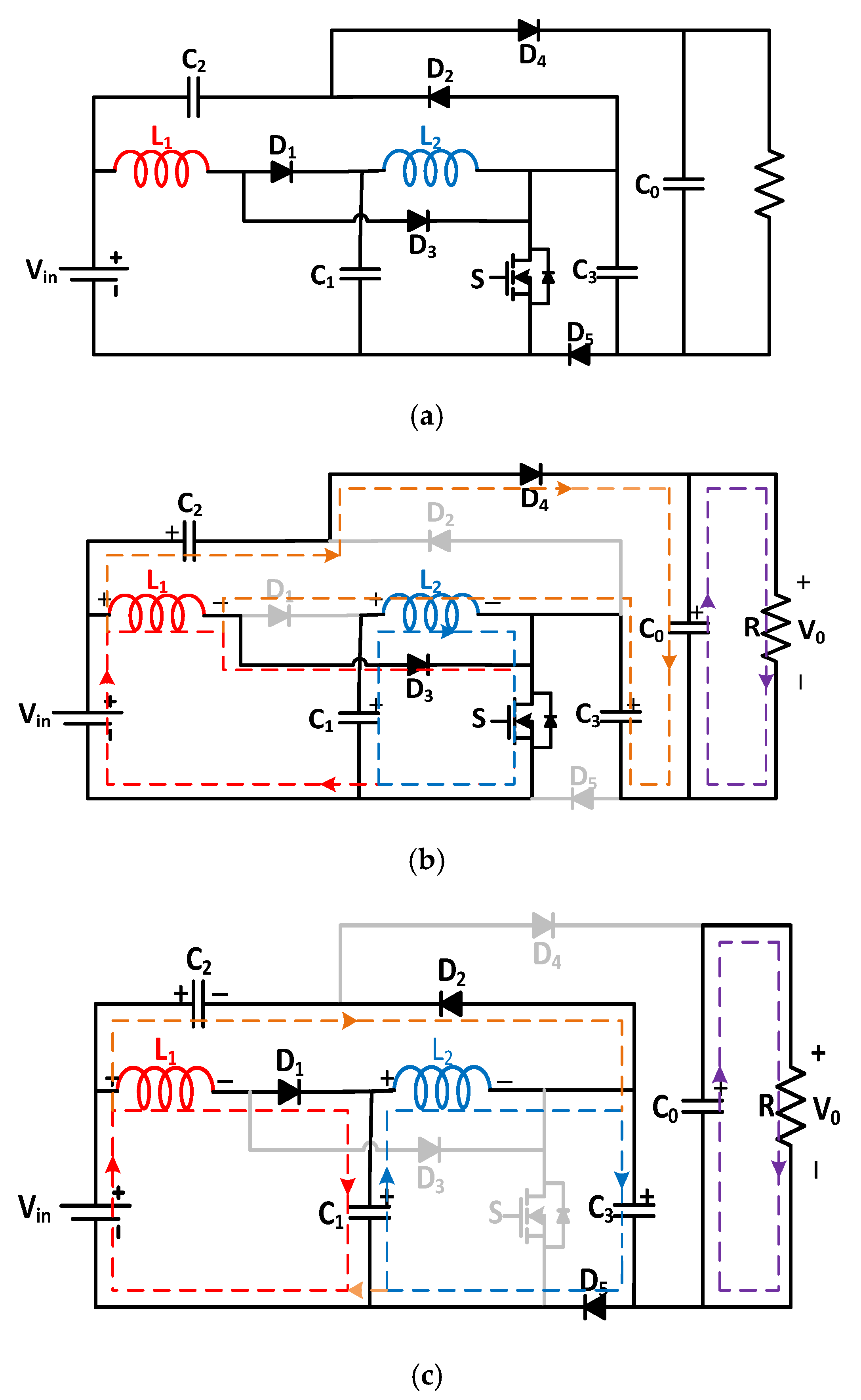
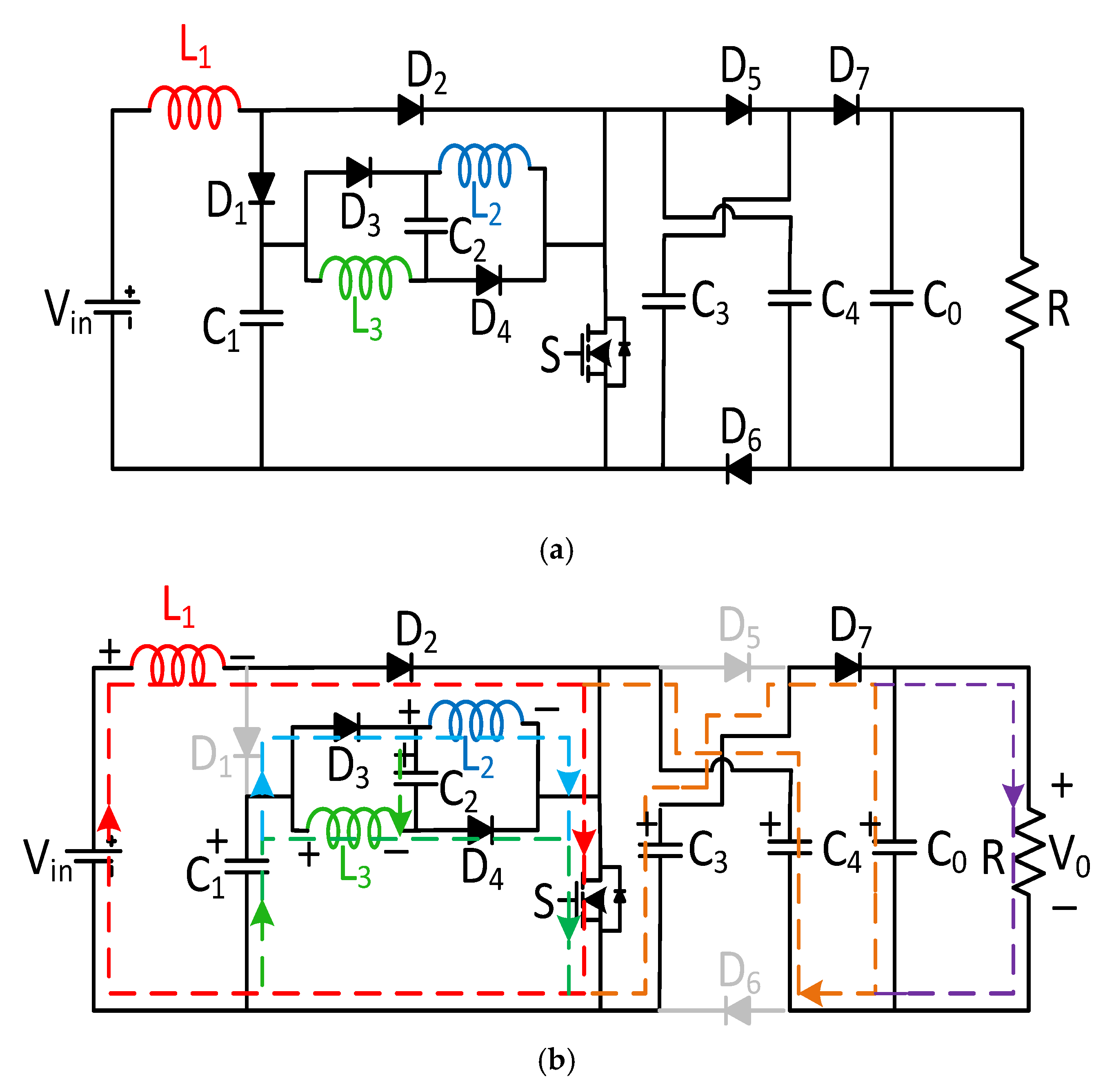
The power circuit in Figure 1a comprises one active switch S, two inductors L1 and L2, four capacitors C1, C2, C3, and Co and five diodes D1, D2, D3, D4, and D5. The converter is operated at high-frequency fs. The network consisting of D2, C2, C3, and D5 constitutes a voltage boosting cell. The advantage of this circuit is that it has a single switch S with lower complexity with continuous input current and utilizing energy with a single input DC source.
2.1. Analysis in CCM Mode
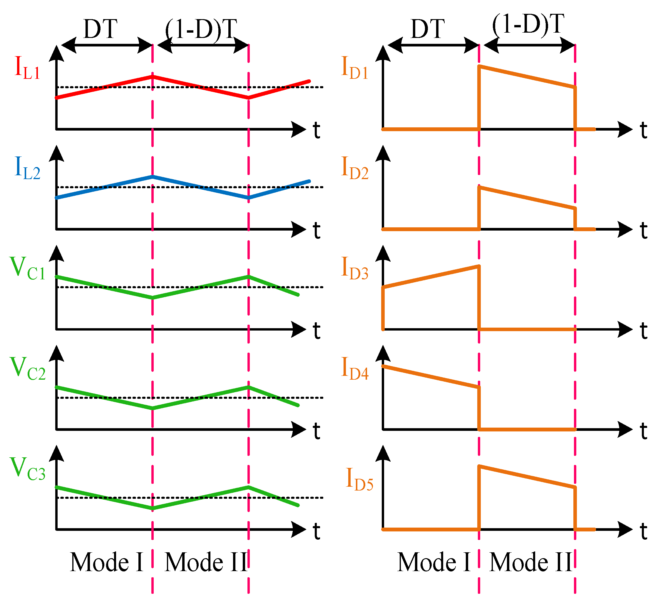
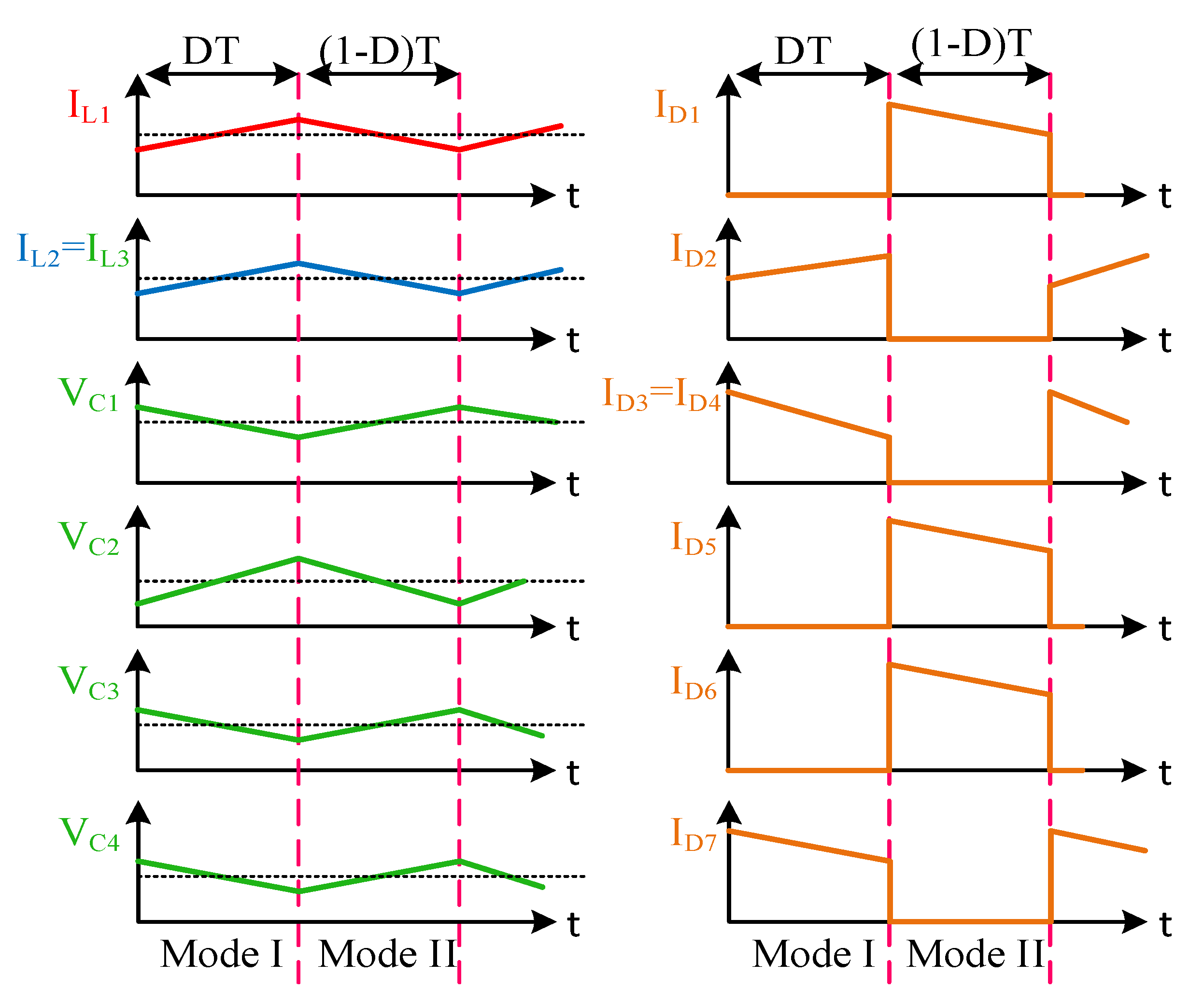
There are two modes of operation based on the switching signal. The first is when the switch is ON, and the second one is when the switch is OFF. Important waveforms for the proposed converter are shown in Figure 2.
2.1.1. MODE I [0-DT]
When the switch S is turned ON, the equivalent circuit is depicted in Figure 1b. The diode D3 and D4 are conducting, and other diodes are reverse biased. Both the inductor currents rise while capacitor C1, C2, and C3 discharge to feed the load R and the related equations are as follows:
2.1.2. MODE II [DT-T]
The switch S is turned OFF, as shown in Figure 1c. The diodes D1, D2, and D5 are conducting and the rest diodes are OFF. The inductor currents fall, and C1, C2, and C3 discharge and load R are fed by Co. The related equations are as follows:
From Equations (1) and (3), we obtain
Applying the principle of voltage–second balance on the inductors L1 and L2
The relations obtained from (6) and (7) can be used to find the voltage gain
It is assumed that the circuit is ideal by applying the energy conservation principle
where is the average current of inductor L1 and is the load current.
The average value of the inductor current can be calculated by applying a charge balance on the capacitor C1.
The current stress on the switch of the proposed converter I is given by (10).
The voltage stress or blocking voltage of a power device is important for deciding the voltage rating of the switch. The voltage stress across the power switch (VS) and diodes (D1, D2, D3, D4, and D5) of the converter I can be derived as
It can be inferred from (11) that the stress across D1, D3, D4, and D5 and switch S is equal to half of the output voltage.
2.2. Passive Components Selection
The peak-to-peak ripple values of the inductor current can be expressed as
With known values of D, the input source , and switching frequency fs, the design values of inductors and can be calculated.
For achieving the boundary condition, and . The condition of continuous conduction mode can be achieved using (9) and (12):
The peak-to-peak ripple across the capacitors C1, C2, C3, and Co is , respectively, and can be expressed as
With known values of D, the input source and switching frequency fs, the design values of capacitances can be calculated from Equation (14).
2.3. Boundary Condition Mode
It is assumed that the inductor current remains continuous while inductor current goes in discontinuous conduction mode with zero current at the end of every switching period.
The DC value of the inductor current can be found as
The boundary normalized inductor time constant on the inductor is defined as
The boundary normalized inductor time can be derived from (10) and (12):
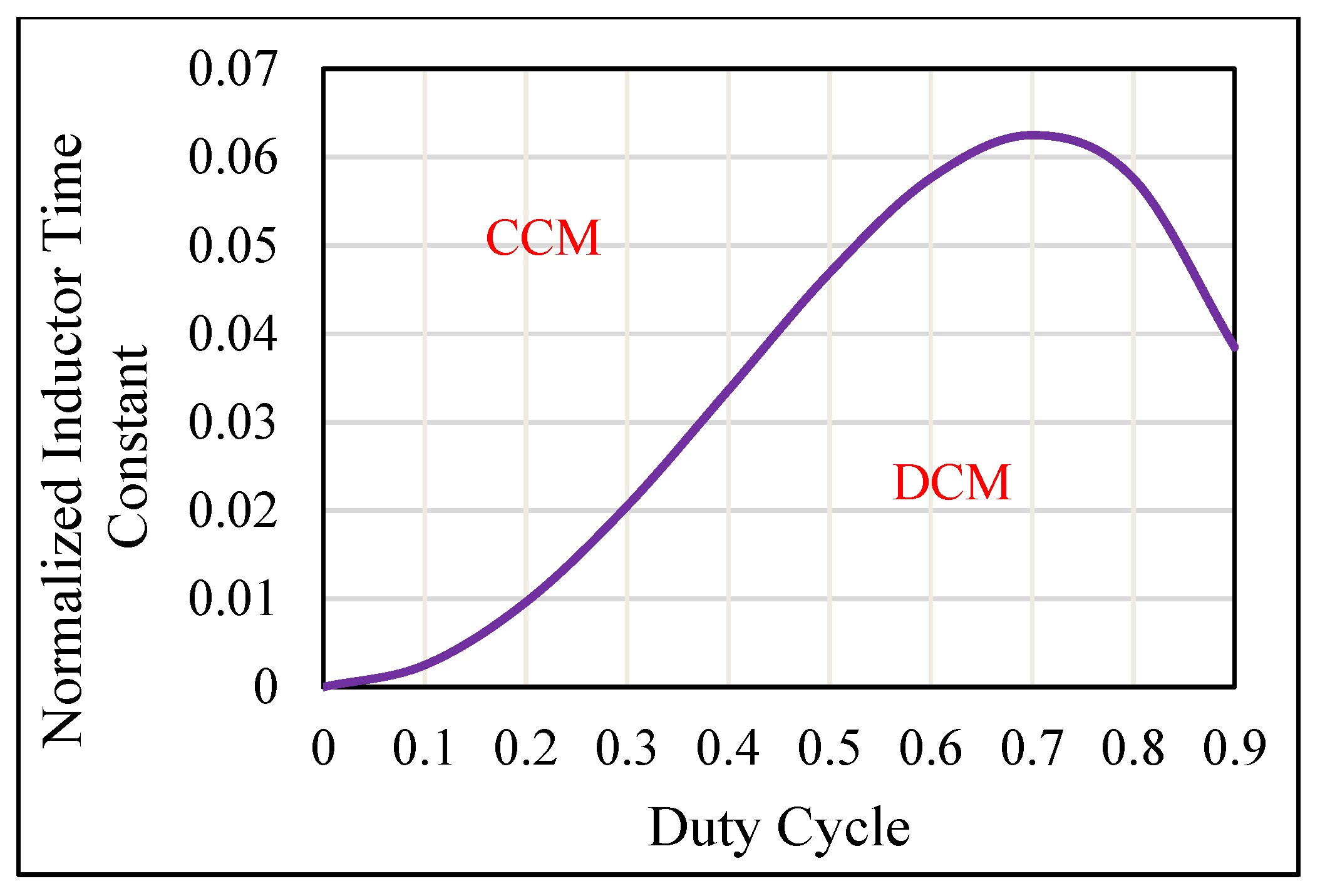
To operate the converter in CCM mode, must be greater than Otherwise, the converter goes in DCM, as depicted in Figure 3.
3. Proposed Converter II
The proposed converter II is shown in Figure 4a and has an equal number of components of converter I. The power circuit consists of one switch s, two inductors L1 and L2, five diodes D1, D2, D3, D4, and D5, and four capacitors C1, C2, C3, and an output capacitor Co supplying energy to load R. The proposed converter has the inductor on the input side, which makes the current continuous with very low ripple.
3.1. Analysis in CCM Mode
The two modes of operation follow.
3.1.1. Mode I [0-DT]
When the switch is turned ON, the equivalent circuit is depicted in Figure 4b. The diodes D2 and D5 are conducting while D1, D3, and D4 are reversed biased. The switch S is conducting an interval of DT where D is the duty ratio, and T is the switching signal period. The currents of both inductors rise and capacitors C1, C2, and C3 discharge to charge output capacitor C0 to feed load R. The related equations follow:
3.1.2. Mode II [DT-T]
Contrarily, the switch is in OFF condition, and diodes D1, D3, and D4 are conducting while diode D2 and D5 are in reverse biased, as shown in Figure 4c. The important waveforms for this converter are shown in Figure 5. The switch is conducting for an interval of (1 − D) T. The currents of both inductors fall to charge capacitors C1, C2, and C3, while C0 separately feeds the load R. The related equations follow:
Using (15) and (17), the capacitor voltages are
Applying the principle of voltage–second balance on the inductors L1 and L2 by using (14)–(18) gives
Results obtained from (20) and (21) are used to find voltage gain of the proposed converter II:
It is assumed that the circuit is ideal by applying the energy conservation principle:
where is the average current of inductor L1 and is the load current.
The average value of the inductor current could be calculated by applying charge balance on the capacitor C1:
The current stress on the switch of proposed converter II is given by (27). The voltage stress or blocking voltage of a power device is important to decide the ratings of the semiconductor devices. The stress of the power switch (VS) and across D1, D2, D3, D4, and D5 of the converter II can be shown as follows
It can be inferred from (28) that the stress across diodes D1, D3, D4, and D5 and switch S is equal and half of the output voltage.
3.2. Passive Component Selection
The peak-to-peak ripple values of the inductor current can be expressed as
With known values of D, the input source and switching frequency fs, the design values of inductors and can be calculated.
The boundary condition is achieved when the minimum inductor current reaches zero, i.e., and . The condition of continuous conduction mode can be achieved as
The peak-to-peak ripple across the capacitors C1, C2, C3, and Co is , respectively, and can be expressed as
With known values of D, the input source , and switching frequency fs, the design values of capacitances can be calculated using (31) with the assumption of C2 = C3.
3.3. Boundary Condition
It is assumed that the inductor current remains continuous while inductor current goes in discontinuous conduction mode with zero current at the end of every switching period.
The DC value of the inductor current can be found as
The boundary normalized inductor time constant on the inductor is defined as
The boundary normalized inductor time can be derived from (27) and (29):
To operate the converter in CCM mode, must be greater than ; otherwise, the converter goes in DCM, as depicted in Figure 6.
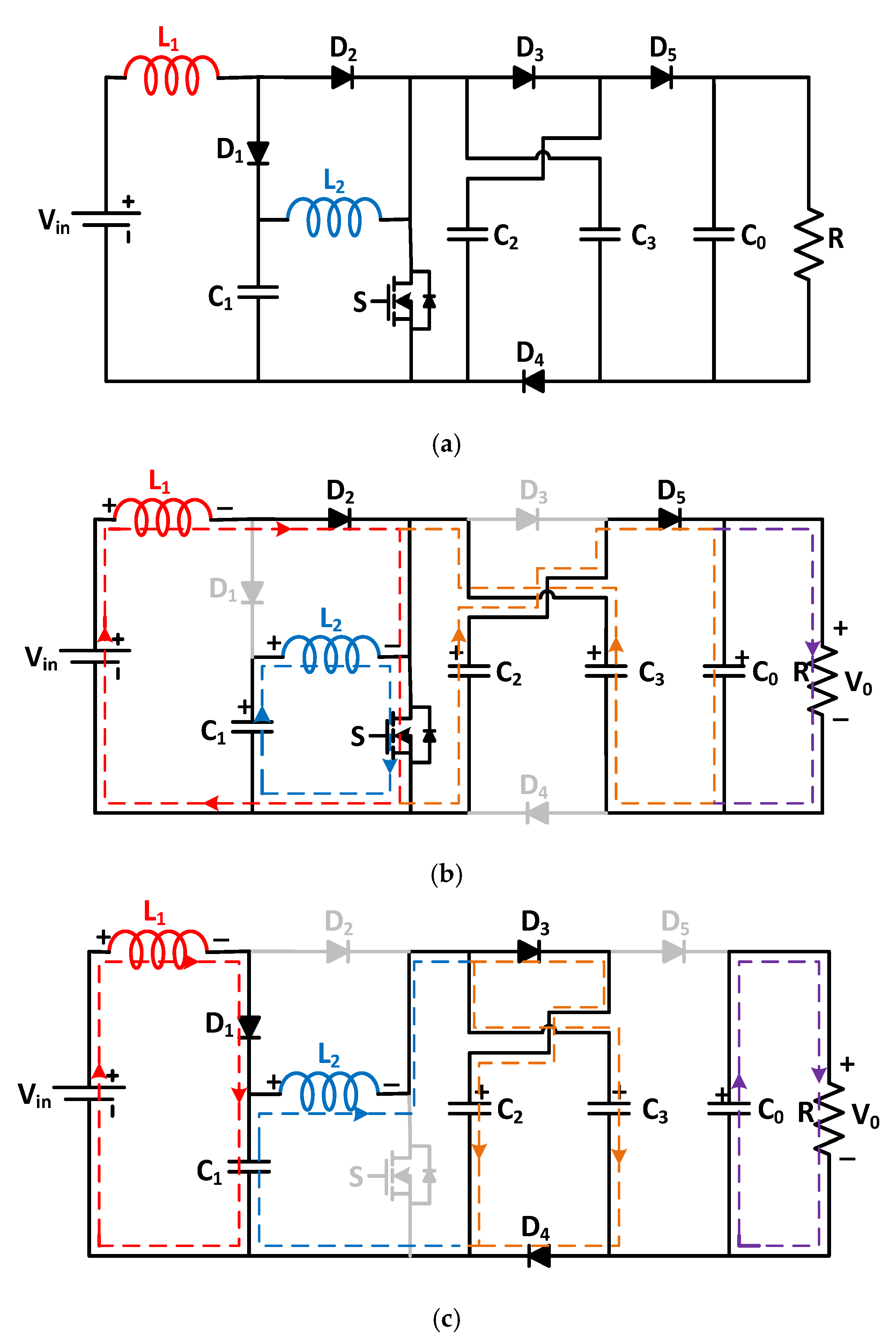
4. Proposed Converter III
Proposed converter III is an extension of proposed converter II in which inductor L2 is replaced with a switched inductor boost cell consisting of D3, D4, L2, and L3 as shown in Figure 7a, with single switch S and energy increased by boosting cell to feed load R. The proposed converter has two voltage multiplier cells that increase output voltage by four times.
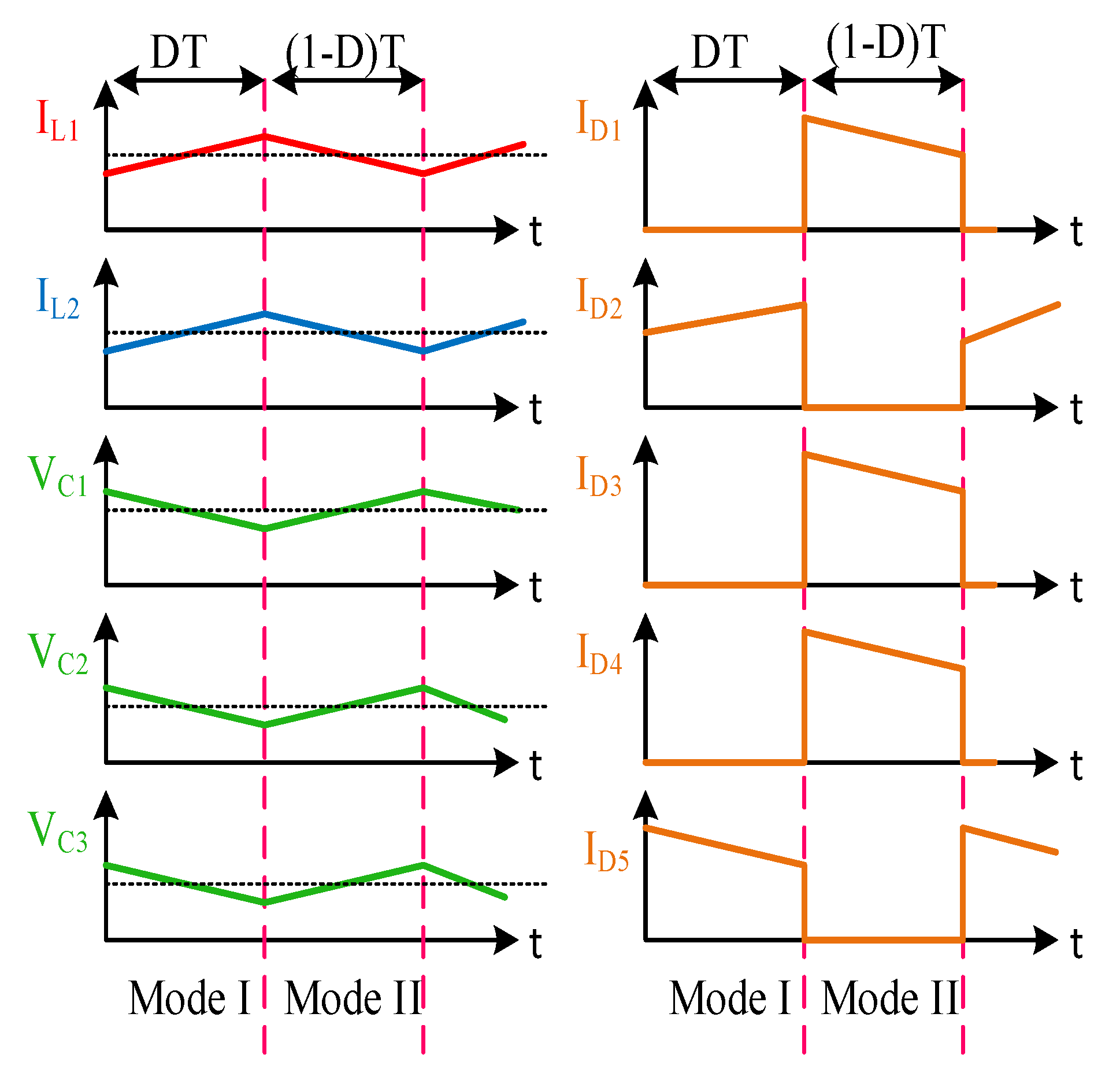
4.1. Analysis in CCM Mode
The continuous conduction mode of the converter can be discussed in detail with two modes of operation.
4.1.1. Mode I [0-DT]
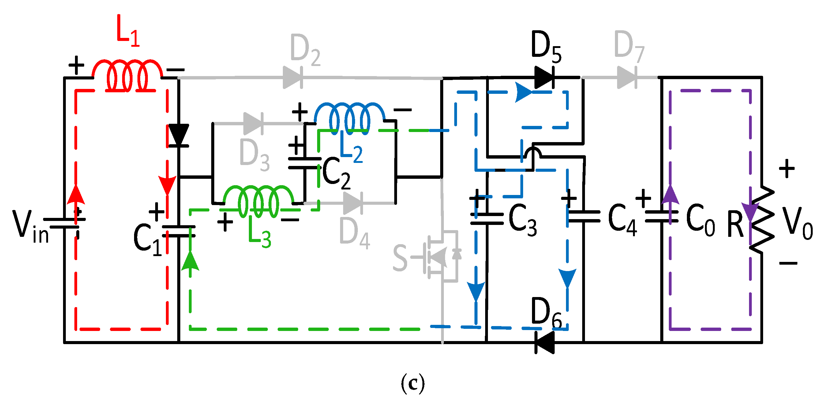
When the switch is turned ON, the equivalent circuit is depicted in Figure 7b and Figure 8. The diodes D2, D3, D5, and D7 are conducting while D1, D5, and D6 are reversed biased. All three inductor currents rise and capacitors C1 to C4 discharge to feed the load R. The switch S conducts for the DT period. The related equations follow:
4.1.2. Mode I [DT-T]
Contrarily, the switch is in OFF condition, and diodes D1, D5, and D6 are conducting while diode D2, D3, D5, and D7 are in reverse biased, as shown in Figure 7c and Figure 8. The switch is conducting for an interval of (1-D) T. Both the inductor currents fall to charge capacitors C1, C2, and C3, while C0 separately feeds the load R. The related equations follow:
Applying the principle of voltage–second balance on the inductors L1 and L2 and L3 and by using (33)–(36), Vo and VC1 can be obtained as shown in (39) and (40).
Results obtained from (37) and (38) are used to find the voltage gain of the proposed converter III:
It is assumed that the circuit is ideal by applying the energy conservation principle:
where is the average current of inductor L1 and is the load current.
The DC component of the inductor currents of L2 and L3 ( can be calculated by applying charge balance on capacitors C1 and C2:
The current stress on the switch of the proposed converter III is given by (43). The voltage stress or blocking voltage of a power device is important to decide the semiconductor device rating.
The stress of the power switch(S) and diodes of the converter III can be derived as
It can be inferred from (44) that the stress across D5, D6, D7 and S is equal and half of the output voltage.
4.2. Passive Component Selection
The peak-to-peak ripple values of the inductor current and capacitor voltages can be expressed as
With known values of D, the input source , and switching frequency fs, the design values of inductors and can be calculated.
The boundary condition is achieved when the minimum inductor current reaches zero, i.e., and . The condition of continuous conduction mode can be achieved as
The peak-to-peak ripple across the capacitors C1, C2, C3, C4, and Co are , respectively, and can be expressed as
With known values of D, the input source , and switching frequency fs, the design values of capacitances can be calculated using (47) with the assumption of C3 = C4.
4.3. Boundary Condition
It is assumed that the inductor current remains continuous while inductor current goes in discontinuous conduction mode with zero current at the end of every switching period.
The DC value of the inductor current in this mode can be found as
The boundary normalized inductor time constant on the inductor is defined as
The boundary normalized inductor time can be derived from (43) and (45):
To operate the converter in CCM mode, must be greater than Otherwise, the converter goes in DCM, as depicted in Figure 9.
5. Comparison of the Proposed Topologies
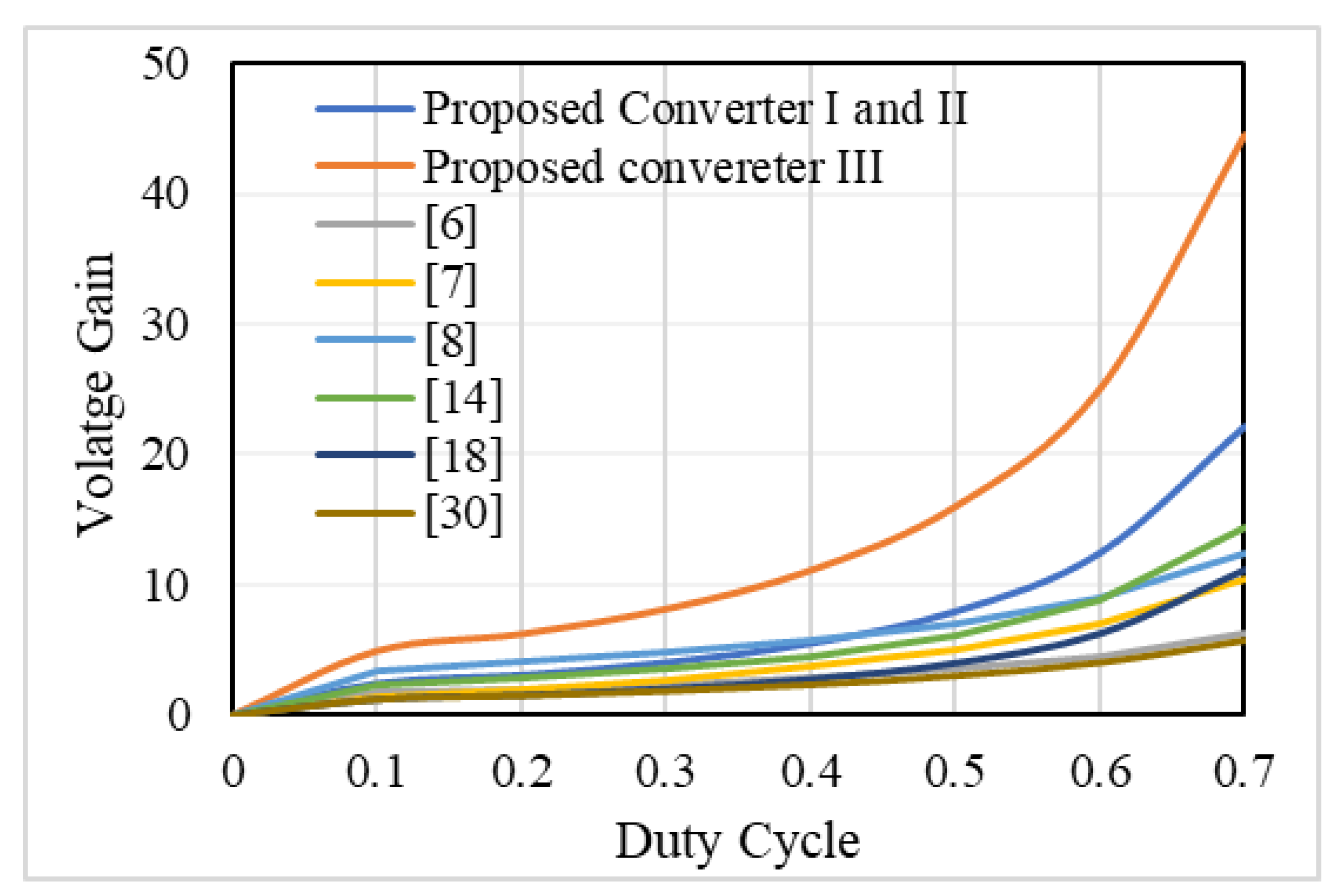
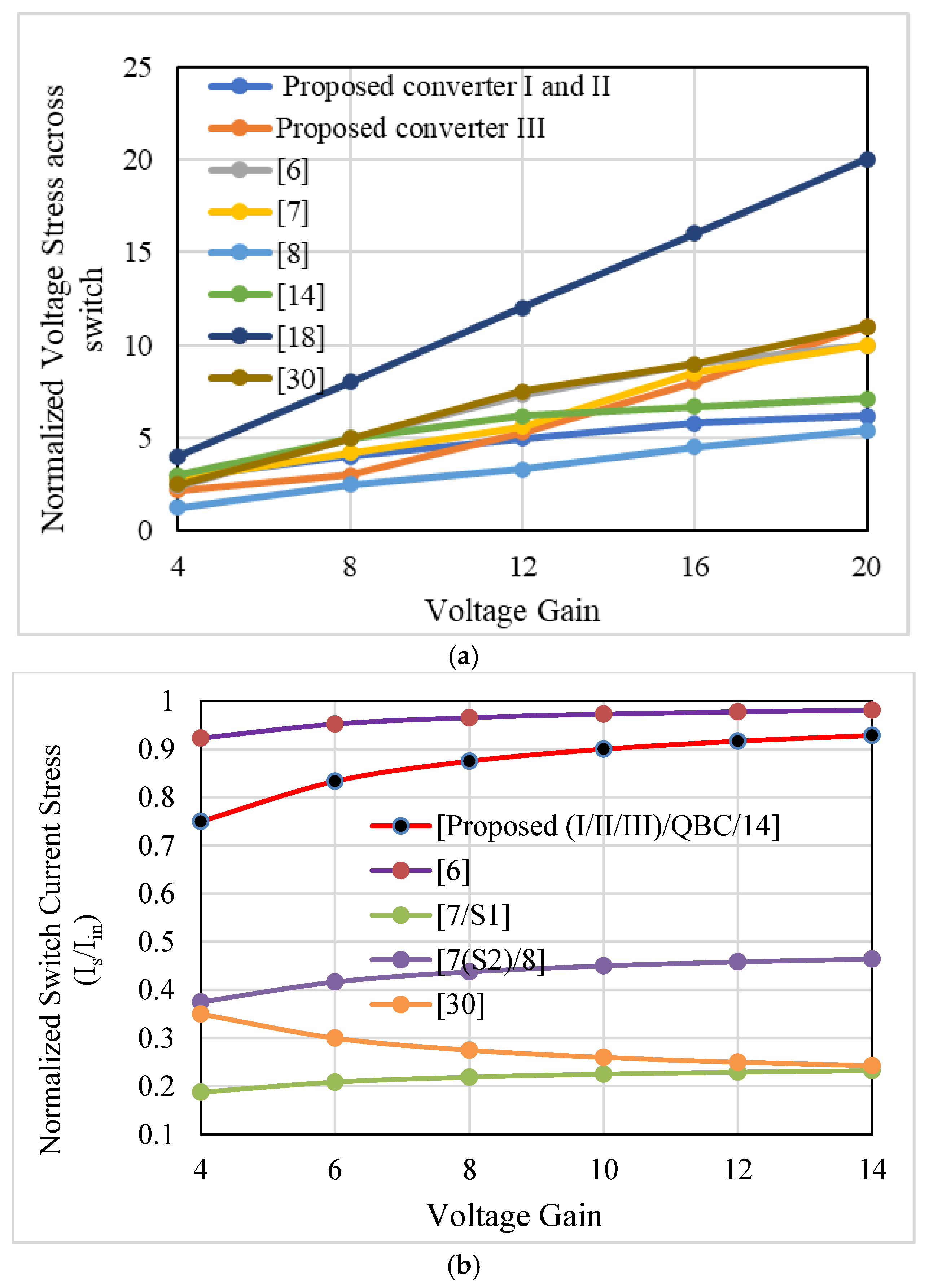
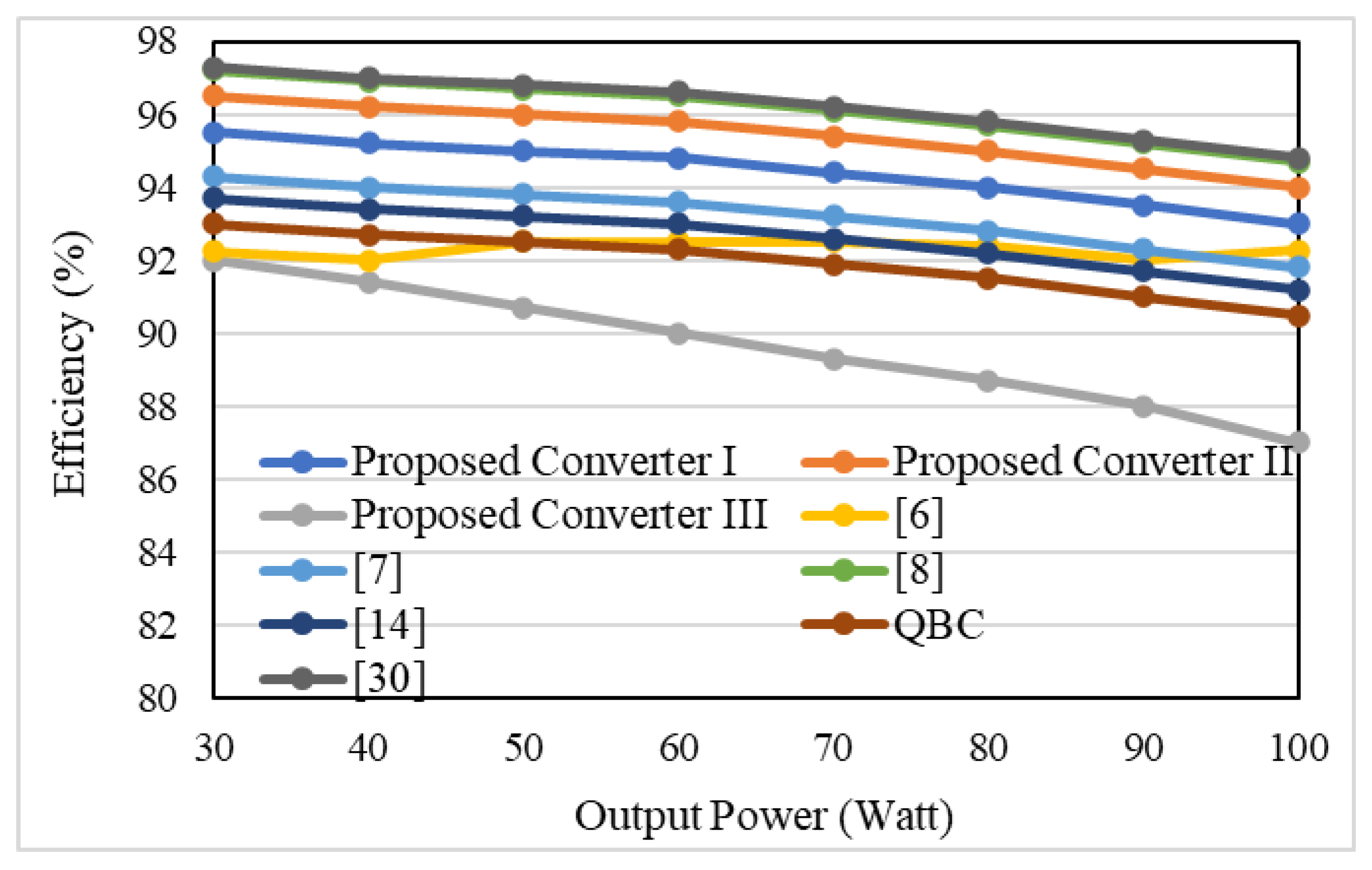
Several DC-DC converters have been proposed to achieve high gain and improved high efficiency. In this section, the comparison of the proposed converter with other recently introduced topologies in Table 2 is shown. The converters are compared based on voltage gain, switch voltage stress, current stress, and component count. Converter I and III have lower components than the proposed converter in [7]. The proposed converter in [30] has more components than all the proposed converters. In addition, it utilizes many power switches, which makes the circuit bulky. The curve of the proposed converter III is the highest among all the curves of Figure 10. Proposed converters I and II also have a high voltage gain compared to the other topologies above D = 0.3. The gain of converters I and II is also high as compared to other converters, which substantially increases above D = 0.4. The proposed converter in [7] has three inductors, but the gain is much less than the proposed family of converters. Similarly, the topology of [8] uses two inductors, but the gain is limited at higher duty ratios. The conventional quadratic boost converter (QBC) has a low gain compared to the proposed topologies. The voltage stress across the switch as a function of voltage gain is shown in Figure 11a. As the gain increases, the voltage stress across the switch of converters I and II is much less than the other topologies, except for the topologies proposed in [8,30]. Moreover, for voltage gain up to 12 times, the stress across the converter III is less than other converters proposed in [6,7,14,18,30]. The low voltage stress across components results in increased efficiency and low cost of the converter. The efficiency of the converter depends on factors such as voltage/current ratings, components count, and the type of converter. The comparison concerning the switch current stress is shown in Figure 11b. The proposed converters have lower current stress than the converter proposed in [6]. The switch current stress of all three proposed converters and the converter presented in [14] is the same as QBC, but QBC has low voltage gain and high voltage stress. The curve in Figure 12 presents the variation of efficiency with the output power at constant load resistance. The efficiency of proposed converter I and II is higher as compared to the proposed converter III. This is because of the presence of more components in the third topology. The efficiency of all three converters decreases with the increase in the output power. With the rise in the output power, the current in the internal circuit increases, which increases the conduction losses in the circuit. The efficiency of proposed converter II is greater than I, III, [6,7,8,14], and quadratic boost converter (QBC). The converter [18] has the highest efficiency among the listed converters because it has the lowest current and voltage stress on the switch, but it has a more components, which makes the circuit bulky.
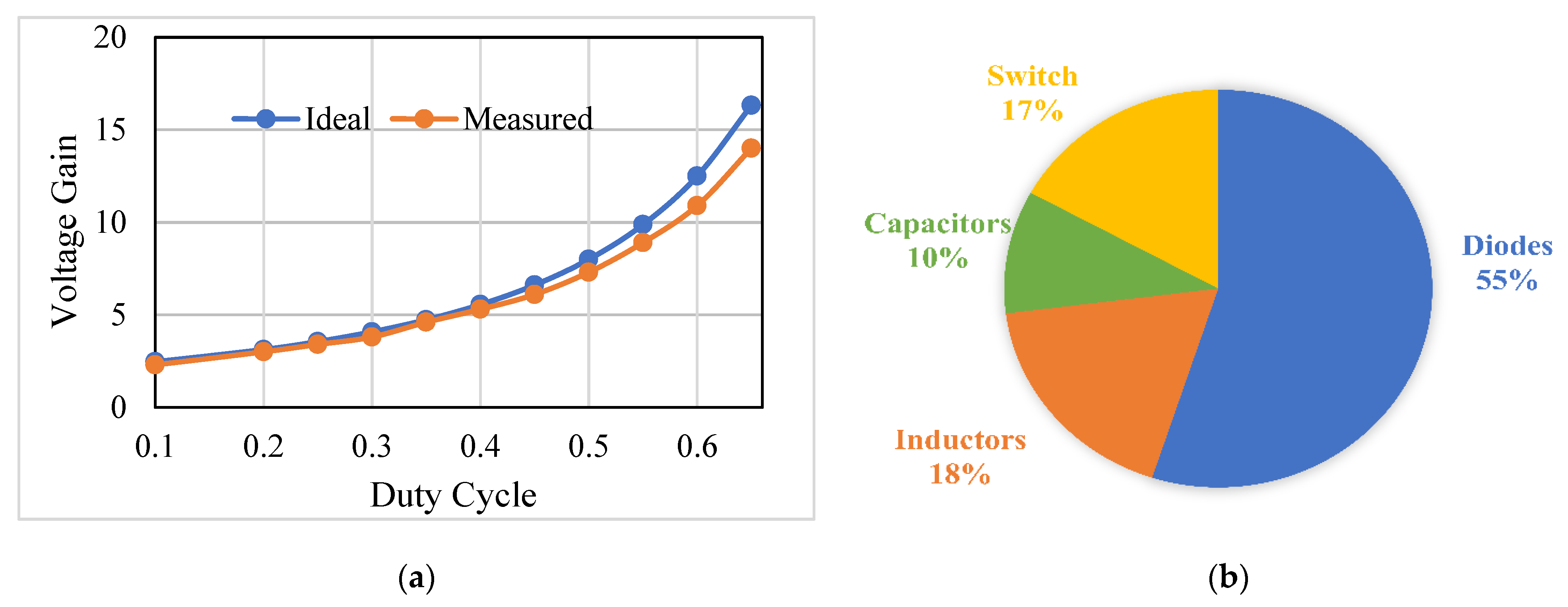
The measured and ideal voltage gain for converters I and II are presented in Figure 13a. At lower duty, the difference between the ideal and measured voltage gain is very low; however, the difference increases with the duty ratio increase. This happens because, at a higher duty ratio, the internal losses in the circuit become higher. The measured gain is taken in experimental conditions. Loss calculation is done on PLECS software by putting the switching and conduction loss data into the lookup table of the developed thermal model. In PLECS software, accurate loss analysis can be done by using the real models of switches and diodes from the datasheet to calculate the conduction and switching losses. The bifurcation of power loss in different components for converter I and II are shown in Figure 13b.
6. Experimental Verification of the Proposed Converters
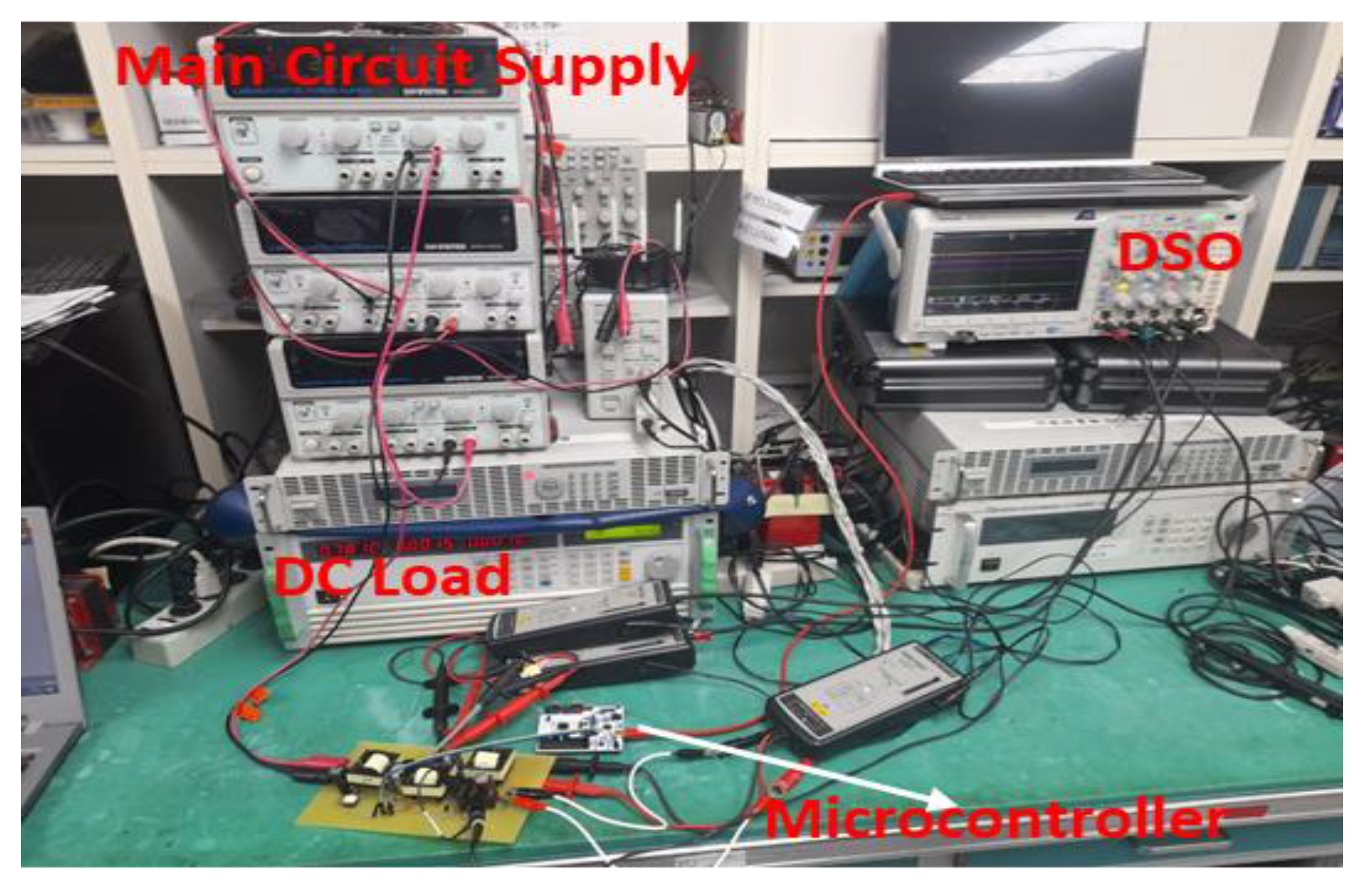
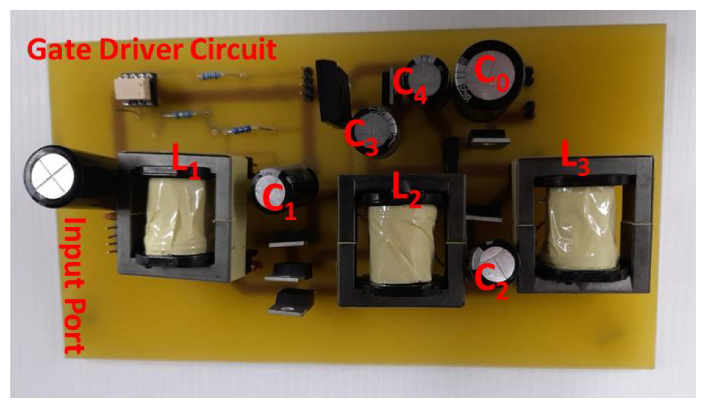
The laboratory prototype of each proposed converter was developed and tested under laboratory conditions. The hardware setup is shown in Figure 14.
6.1. Proposed Converter I
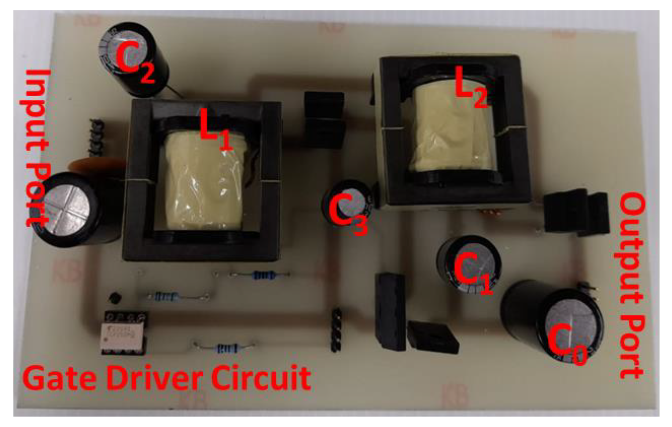
The design specification of the proposed converter I is presented in Table 3. The laboratory hardware prototype of the converter is shown in Figure 15.
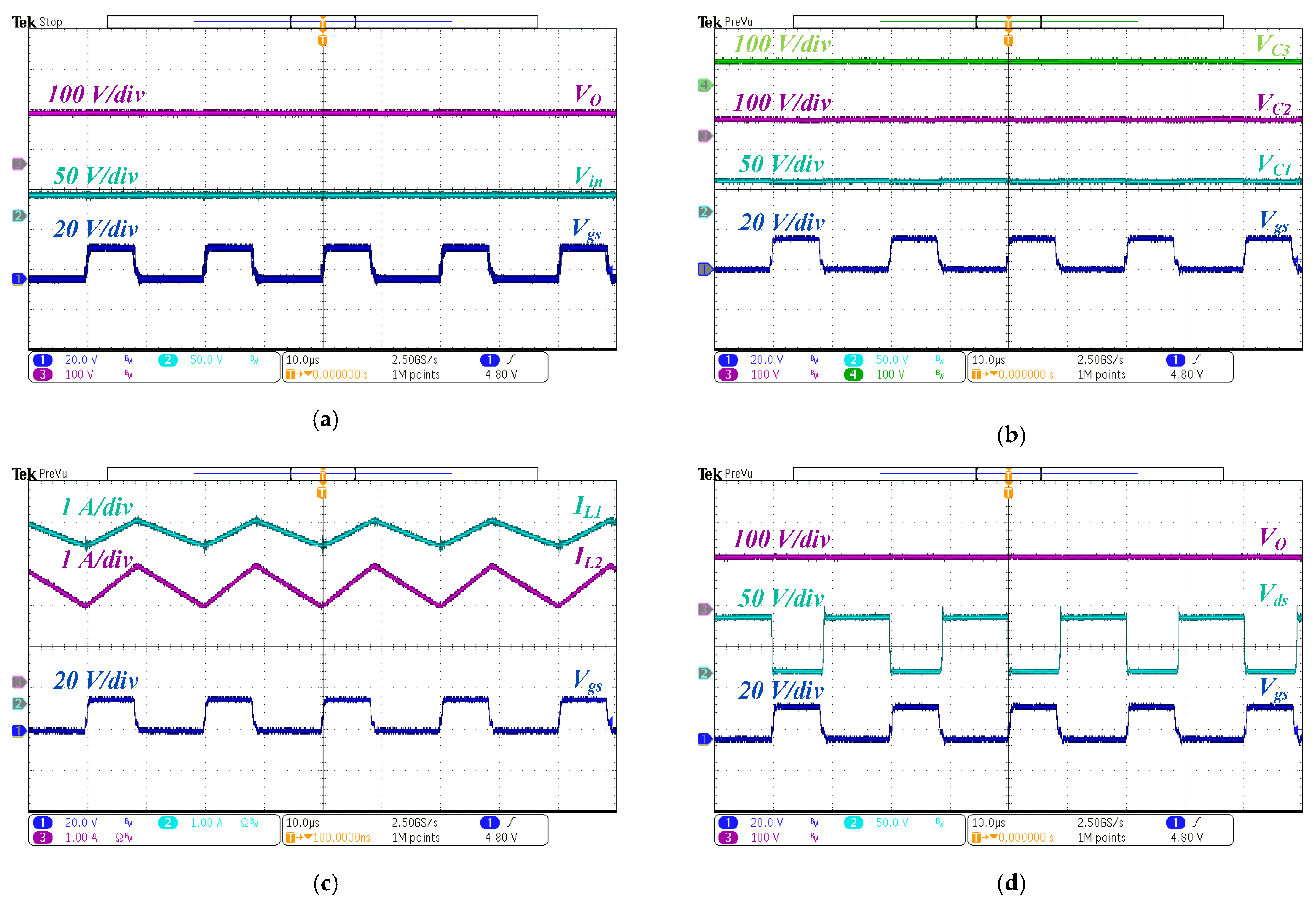
The results shown in Figure 16 are shown at a duty ratio of 0.4 with a load resistance of 200 Ω.
6.2. Proposed Converter II
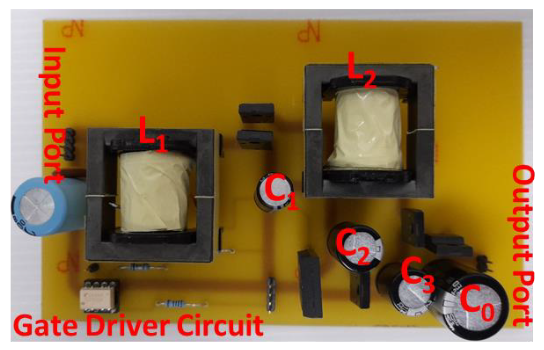
The design specification of the proposed converter II is presented in Table 4. The laboratory hardware prototype of the converter is shown in Figure 17.
The results shown in Figure 18 are taken at a duty ratio of 0.4 with a load resistance of 350 Ω.
6.3. Proposed Converter III
The design specification of the proposed converter III is presented in Table 5. The laboratory hardware prototype of the converter is shown in Figure 19.
The results shown in Figure 20 are taken at a duty ratio of 0.2 with a load resistance of 350 Ω.
In the first converter case, the hardware prototype’s measured output voltage is 127 volts at a 0.4 duty ratio. However, in the second topology, the output voltage is measured as 130 volts at the same input voltage and duty ratio as that of the first converter; due to higher load resistance, the voltage is higher in the second converter case. In the first converter case, the load resistance is only around 60% of the load resistance, as in the second converter case. Thus, the current is high in the first converter circuit, which increases the first converter’s internal losses compared to that of the second converter. With the increase in the load current, the output voltage decreases because of the rise in the circuit’s internal losses.
In the third converter case, the measured output voltage is 128 volts at a duty ratio of 0.2 and load resistance of 200 Ω, which is almost 15% lower than the calculated voltage for the ideal condition. The deviation from the ideal voltage is the same as explained before, which is internal power loss. These internal losses depend on the number of components in the circuit, ESR (equivalent series resistance) of the passive components, diode forward voltage drop, switching frequency and load, etc. The findings of the experimental results are provided in Table 6.
7. Conclusions
The paper presents three different high gain DC-DC converter topologies of the quadratic gain family. While two of the topologies have twice the quadratic boost gain, the third has four times the quadratic boost gain, making them extremely effective for low duty high gain operation at high efficiency. None of the topologies uses any transformers and has a gain of more than ten times at a duty ratio of less than 0.5. Topology II is found to have comparatively high efficiency as compared to topology 1 and III. The stress in switches in the three topologies are less for a wide operating range as compared to many recently proposed high gain quadratic converters. The efficiency of converter I and converter II at 100 W is found to be 92% and 93.2% respectively. The efficiency of converter III is close to 87%. The continuous input current along with reduced voltage stress makes all of the proposed topologies suitable for renewable energy applications.
Author Contributions
Conceptualization, M.Z. and J.A.; methodology, M.Z, S.K., J.A. and M.T.; software, A.A., A.M., S.K. and A.S.; validation, J.A., A.S. and M.T.; formal analysis, J.A.; A.M. and S.K.; investigation, A.S., M.T., B.A. and A.A.; resources, C.-H.L., M.T. and B.A.; data curation, A.S. and A.M.; writing—original draft preparation, S.K. and M.Z.; writing—review and editing, M.Z., J.A. and A.M.; visualization, M.T. and A.S.; supervision, C.-H.L., B.A. and A.A.; project administration, C.-H.L., B.A. and A.A.; funding. C.-H.L., B.A., M.T. and A.A. All authors have read and agreed to the published version of the manuscript.
Funding
This research was funded in part by Taif University Researchers Supporting Project Number (TURSP-2020/121), Taif University, Taif, Saudi Arabia, and in part by the collaborative research grant scheme (CRGS) project granted by the capability systems centre, UNSW-Canberra at ADFA to the Hardware-In-the-Loop (HIL) Laboratory, Department of Electrical Engineering, Aligarh Muslim University, India, project number CRGS/MOHD TARIQ/01. The APC was funded by NTUST, Taiwan.
Acknowledgments
The authors also acknowledge the support provided by the Hardware-In-the-Loop (HIL) Laboratory and Non-Conventional Energy (NCE) Laboratory, Department of Electrical Engineering, Aligarh Muslim University, India.
Conflicts of Interest
The authors declare no conflict of interest.
References
- Forouzesh, M.; Siwakoti, Y.P.; Gorji, S.A.; Blaabjerg, F.; Lehman, B. Step-Up DC–DC Converters: A Comprehensive Review of Voltage-Boosting Techniques, Topologies, and Applications. IEEE Trans. Power Electron. 2017, 32, 9143–9178. [Google Scholar] [CrossRef]
- Maroti, P.K.; Padmanaban, S.; Holm-Nielsen, J.B.; Bhaskar, M.S.; Meraj, M.; Iqbal, A. A New Structure of High Voltage Gain SEPIC Converter for Renewable Energy Applications. IEEE Access 2019, 7, 89857–89868. [Google Scholar] [CrossRef]
- Shayeghi, H.; Pourjafar, S.; Hashemzadeh, S.M. A switching capacitor based multi-port bidirectional DC–DC converter. IET Power Electron. 2021. [Google Scholar] [CrossRef]
- Sadaf, S.; Bhaskar, M.S.; Meraj, M.; Iqbal, A.; Al-Emadi, N. A Novel Modified Switched Inductor Boost Converter With Reduced Switch Voltage Stress. IEEE Trans. Ind. Electron. 2021, 68, 1275–1289. [Google Scholar] [CrossRef]
- Shahir, F.M.; Babaei, E.; Farsadi, M. Extended Topology for a Boost DC–DC Converter. IEEE Trans. Power Electron. 2019, 34, 2375–2384. [Google Scholar] [CrossRef]
- Saravanan, S.; Babu, N.R. Design and Development of Single Switch High Step-Up DC–DC Converter. IEEE J. Emerg. Sel. Top. Power Electron. 2018, 6, 855–863. [Google Scholar] [CrossRef]
- Tang, Y.; Fu, D.; Wang, T.; Xu, Z. Hybrid Switched-Inductor Converters for High Step-Up Conversion. IEEE Trans. Ind. Electron. 2015, 62, 1480–1490. [Google Scholar] [CrossRef]
- Tang, Y.; Wang, T.; He, Y. A Switched-Capacitor-Based Active-Network Converter with High Voltage Gain. IEEE Trans. Power Electron. 2014, 29, 2959–2968. [Google Scholar] [CrossRef]
- Arunkumari, T.; Indragandhi, V.; Arunkumar, G.; Sanjeevikumar, P.; Holm-Nielsen, J.B. Implementation of a high-gain non-isolated DC-DC converter for PV-fed applications. Int. Trans. Electr. Energy Syst. 2020, 30, 1–18. [Google Scholar] [CrossRef]
- Shanthi, T.; Prabha, S.U.; Sundaramoorthy, K. Non-isolated n-stage High Step-up DC-DC Converter for Low voltage DC Source Integration. IEEE Trans. Energy Convers. 2021. [Google Scholar] [CrossRef]
- Hasanpour, S.; Baghramian, A.; Mojallali, H. Analysis and Modeling of a New Coupled-Inductor Buck–Boost DC–DC Converter for Renewable Energy Applications. IEEE Trans. Power Electron. 2020, 35, 8088–8101. [Google Scholar] [CrossRef]
- Hasanpour, S.; Siwakoti, Y.P.; Mostaan, A.; Blaabjerg, F. New Semiquadratic High Step-Up DC/DC Converter for Renewable Energy Applications. IEEE Trans. Power Electron. 2021, 36, 433–446. [Google Scholar] [CrossRef]
- Moradpour, R.; Tavakoli, A. A DC–DC boost converter with high voltage gain integrating three-winding coupled inductor with low input current ripple. Int. Trans. Electr. Energy Syst. 2020, 30, 1–23. [Google Scholar] [CrossRef]
- Lee, S.; Do, H. Quadratic Boost DC–DC Converter with High Voltage Gain and Reduced Voltage Stresses. IEEE Trans. Power Electron. 2019, 34, 2397–2404. [Google Scholar] [CrossRef]
- Wang, Y.; Qiu, Y.; Bian, Q.; Guan, Y.; Xu, D. A Single Switch Quadratic Boost High Step Up DC–DC Converter. IEEE Trans. Ind. Electron. 2019, 66, 4387–4397. [Google Scholar] [CrossRef]
- Bhaskar, M.S.; Almakhles, D.J.; Padmanaban, S.; Holm-Nielsen, J.B.; Kumar, A.R.; Masebinu, S.O. Triple-Mode Active-Passive Parallel Intermediate Links Converter With High Voltage Gain and Flexibility in Selection of Duty Cycles. IEEE Access 2020, 8, 134716–134727. [Google Scholar] [CrossRef]
- Abdel-Rahim, O.; Funato, H.; Haruna, J. A comprehensive study of three high-gain DC-DC topologies based on Cockcroft-Walton voltage multiplier for reduced power PV applications. IEEJ Trans. Electr. Electron. Eng. 2018, 13, 642–651. [Google Scholar] [CrossRef]
- Farhadi-Kangarlu, M.; Khiavi, A.M.; Neyshabouri, Y. A non-isolated single-input dual-output boost DC–DC converter. IET Power Electron. 2021, 14, 936–945. [Google Scholar] [CrossRef]
- Alzahrani, A.; Ferdowsi, M.; Shamsi, P. A Family of Scalable Non-Isolated Interleaved DC-DC Boost Converters with Voltage Multiplier Cells. IEEE Access 2019, 7, 11707–11721. [Google Scholar] [CrossRef]
- Meraj, M.; Bhaskar, M.S.; Iqbal, A.; Al-Emadi, N.; Rahman, S. Interleaved Multilevel Boost Converter with Minimal Voltage Multiplier Components for High-Voltage Step-Up Applications. IEEE Trans. Power Electron. 2020, 35, 12816–12833. [Google Scholar] [CrossRef]
- Pan, C.; Chuang, C.; Chu, C. A Novel Transformer-less Adaptable Voltage Quadrupler DC Converter with Low Switch Voltage Stress. IEEE Trans. Power Electron. 2014, 29, 4787–4796. [Google Scholar] [CrossRef]
- Padmavathi, P.; Natarajan, S. Single switch quasi Z-source based high voltage gain DC-DC converter. Int. Trans. Electr. Energy Syst. 2020, 30, 1–25. [Google Scholar] [CrossRef]
- Meinagh, F.A.A.; Yuan, J.; Yang, Y. Analysis and design of a high voltage-gain quasi-Z-source DC–DC converter. IET Power Electron. 2020, 13, 1837–1847. [Google Scholar] [CrossRef]
- Martinez, W.; Cortes, C.; Yamamoto, M.; Imaoka, J. Effect of inductor parasitic resistances on the voltage gain of high step-up DC–DC converters for electric vehicle applications. IET Power Electron. 2018, 11, 1628–1639. [Google Scholar] [CrossRef]
- Ahmad, J.; Zaid, M.; Sarwar, A.; Lin, C.-H.; Asim, M.; Yadav, R.K.; Tariq, M.; Satpathi, K.; Alamri, B. A New High-Gain DC-DC Converter with Continuous Input Current for DC Microgrid Applications. Energies 2021, 14, 2629. [Google Scholar] [CrossRef]
- Ahmad, J.; Zaid, M.; Sarwar, A.; Tariq, M.; Sarwer, Z. A New Transformerless Quadratic Boost Converter with High Voltage Gain. Smart Sci. 2020, 8, 1–21. [Google Scholar] [CrossRef]
- Jalilzadeh, T.; Rostami, N.; Babaei, E.; Maalandish, M. Non-Isolated Topology for High Step-Up DC-DC Converters. IEEE J. Emerg. Sel. Top. Power Electron. 2018. [Google Scholar] [CrossRef]
- Hu, D.; Yin, A.; Ghaderi, D. A transformer-less single-switch boost converter with high-voltage gain and mitigated-voltage stress applicable for photovoltaic utilizations. Int. Trans. Electr. Energy Syst. 2020, 30, 1–22. [Google Scholar] [CrossRef]
- Zaid, M.; Ahmad, J.; Sarwar, A.; Sarwer, Z.; Tariq, M.; Alam, A. A Transformerless Quadratic Boost High Gain DC-DC Converter. In Proceedings of the 2020 IEEE International Conference on Power Electronics, Drives and Energy Systems (PEDES), Jaipur, India, 16–19 December 2020; pp. 1–6. [Google Scholar] [CrossRef]
- Babaei, E.; Maheri, H.M.; Sabahi, M.; Hosseini, S.H. Extendable Nonisolated High Gain DC-DC Converter Based on Active–Passive Inductor Cells. IEEE Trans. Ind. Electron. 2018, 65, 9478–9487. [Google Scholar] [CrossRef]
- Mahmood, A.; Zaid, M.; Ahmad, J.; Khan, M.A.; Khan, S.; Sifat, Z.; Lin, C.-H.; Sarwar, A.; Tariq, M.; Alamri, B. A Non-Inverting High Gain DC-DC Converter with Continuous Input Current. IEEE Access 2021, 9, 54710–54721. [Google Scholar] [CrossRef]
Figure 1.
(a) Proposed converter I and operating modes of the converter: (b) Mode I and (c) Mode II.
Figure 1.
(a) Proposed converter I and operating modes of the converter: (b) Mode I and (c) Mode II.

Figure 2.
Typical waveforms of the proposed converter I in CCM.

Figure 3.
Boundary between CCM and DCM mode of operation.

Figure 4.
(a) Proposed converter II and operating modes: (b) switch is ON and (c) switch is OFF.

Figure 5.
Typical waveforms of the proposed converter II in CCM.

Figure 6.
Boundary between CCM and DCM mode of operation.

Figure 7.
(a) Proposed converter III and operating modes: (b) switch is ON and (c) switch is OFF.


Figure 8.
Typical waveforms of the proposed converter II in CCM.

Figure 9.
Boundary between CCM and DCM mode of operation.

Figure 10.
Voltage gain vs. duty cycle.

Figure 11.
(a) Voltage stress vs. voltage gain. (b) Normalized current switch stress vs. voltage gain.
Figure 11.
(a) Voltage stress vs. voltage gain. (b) Normalized current switch stress vs. voltage gain.

Figure 12.
Efficiency vs. output power curve.

Figure 13.
(a) Comparison between the ideal and experimental gain of converters I and II. (b) Bifurcation of power loss in converters I and II.
Figure 13.
(a) Comparison between the ideal and experimental gain of converters I and II. (b) Bifurcation of power loss in converters I and II.

Figure 14.
Hardware testing setup.

Figure 15.
The proposed converter I hardware prototype.

Figure 16.
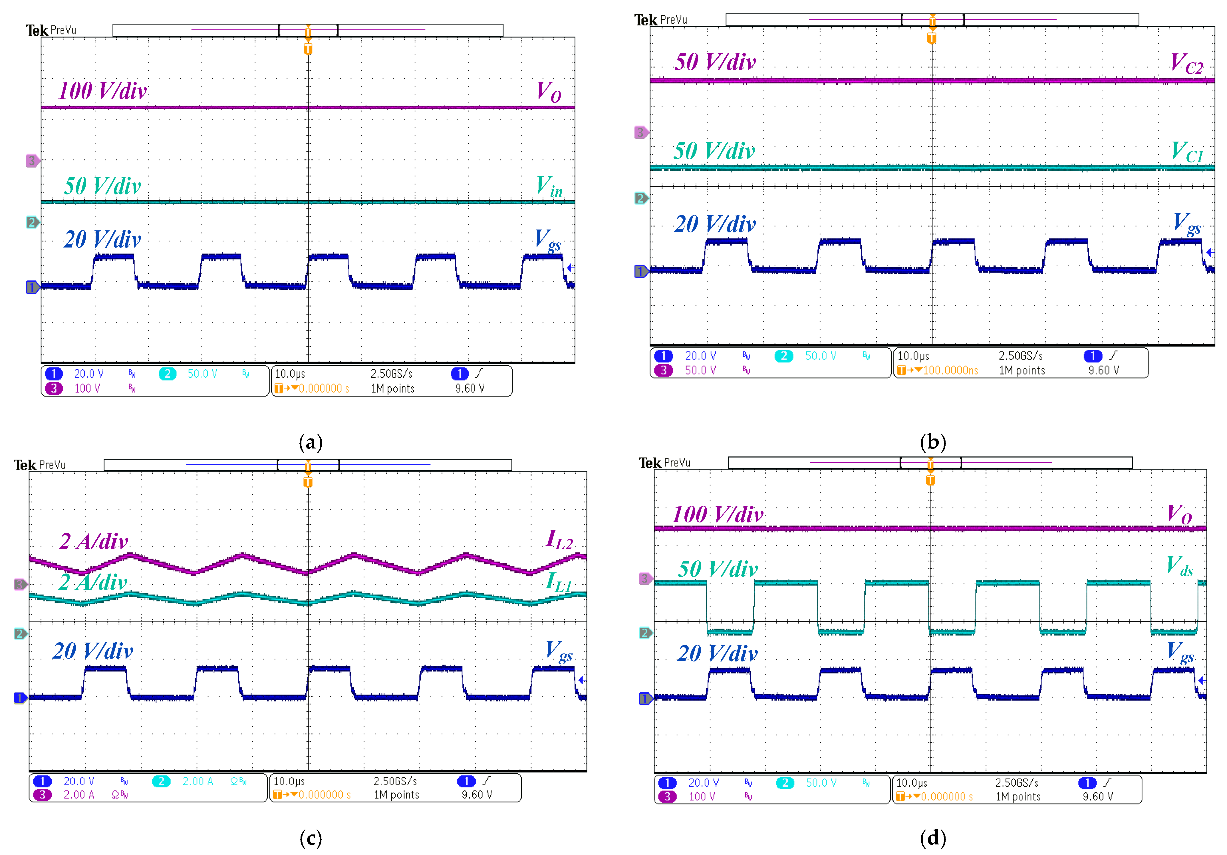
Related waveforms of the experimental results for proposed converter I. (a) Gating pulse, input voltage, and output voltage; (b) gating pulse, voltage for capacitor C1, C2, and C3; (c) gating pulse, inductor current for L1 and L2; and (d) gating pulse, switch voltage, and output voltage.
Figure 16.
Related waveforms of the experimental results for proposed converter I. (a) Gating pulse, input voltage, and output voltage; (b) gating pulse, voltage for capacitor C1, C2, and C3; (c) gating pulse, inductor current for L1 and L2; and (d) gating pulse, switch voltage, and output voltage.

Figure 17.
Proposed converter II hardware prototype.

Figure 18.
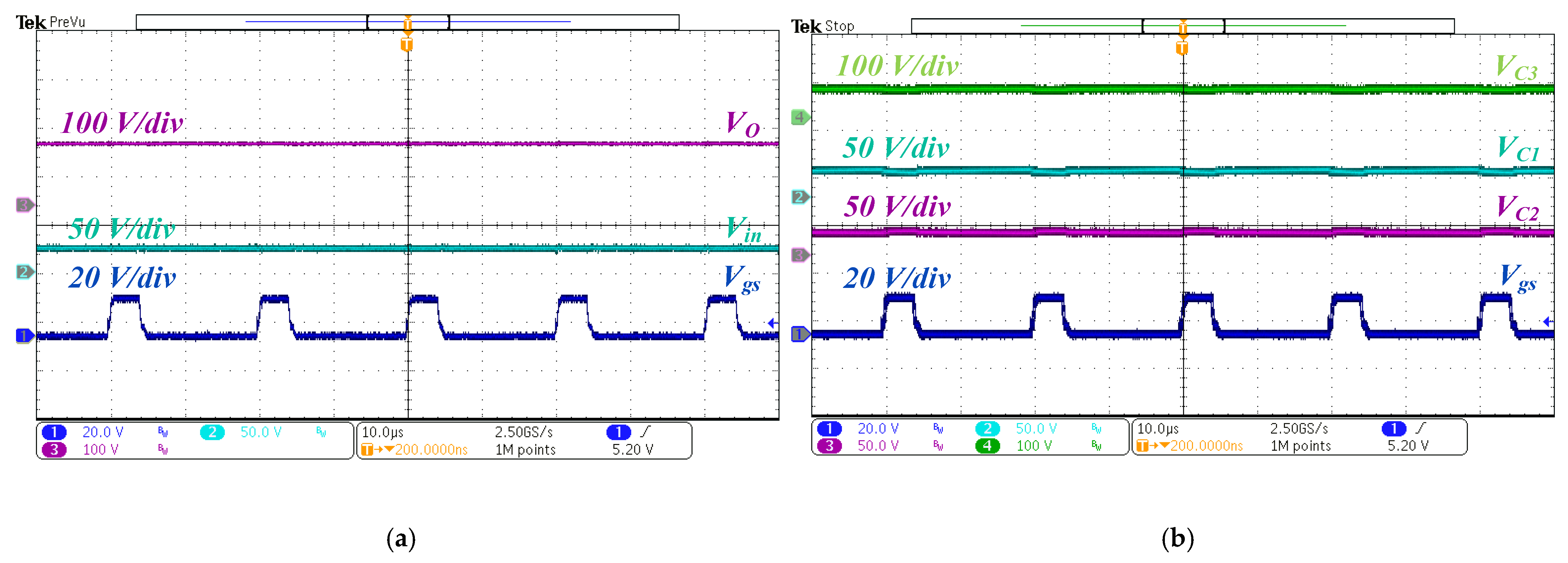
Related waveforms of the experimental results for proposed converter II. (a) Gating pulse, input voltage, and output voltage; (b) gating pulse, voltage for capacitor C1 and C2; (c) gating pulse, inductor current for L1 and L2; and (d) gating pulse, switch voltage, and output voltage.
Figure 18.
Related waveforms of the experimental results for proposed converter II. (a) Gating pulse, input voltage, and output voltage; (b) gating pulse, voltage for capacitor C1 and C2; (c) gating pulse, inductor current for L1 and L2; and (d) gating pulse, switch voltage, and output voltage.

Figure 19.
Proposed converter III hardware prototype.

Figure 20.
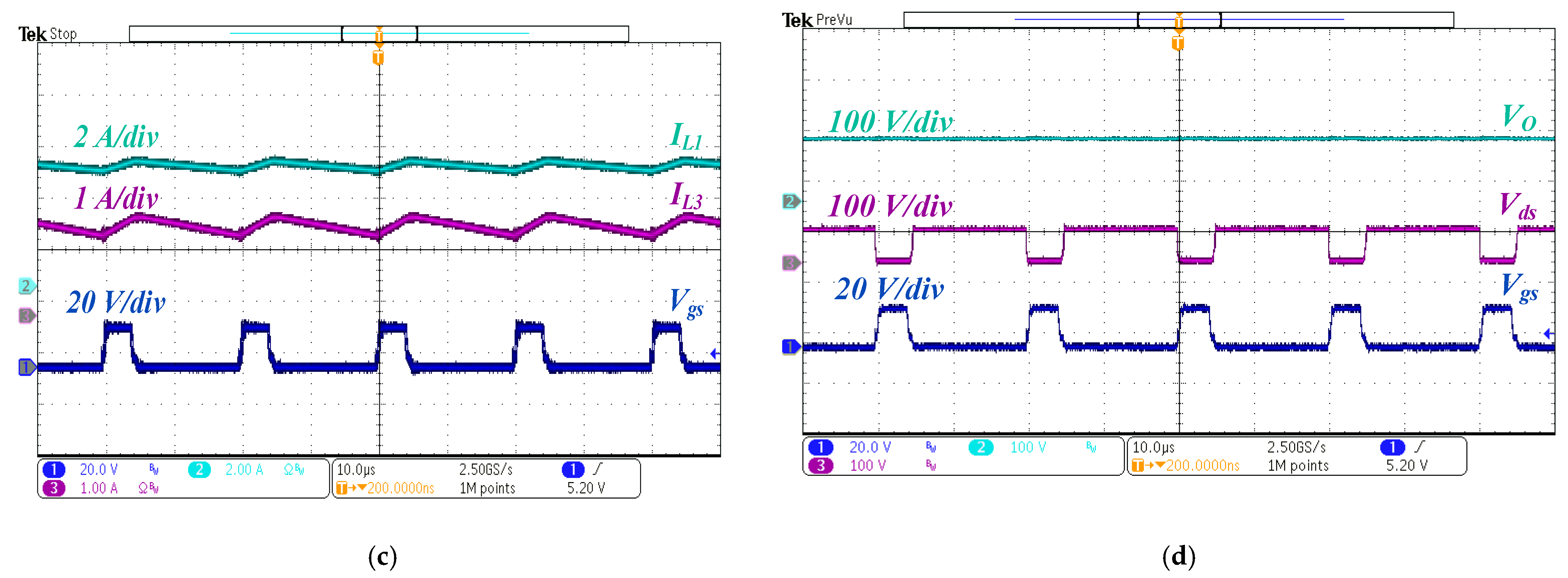
Related waveforms of the experimental results for proposed converter III. (a) Gating pulse, input voltage, and output voltage; (b) gating pulse, voltage for capacitors C1, C2, and C3; (c) gating pulse, inductor current for L1 and L3; and (d) gating pulse, switch voltage and output voltage.
Figure 20.
Related waveforms of the experimental results for proposed converter III. (a) Gating pulse, input voltage, and output voltage; (b) gating pulse, voltage for capacitors C1, C2, and C3; (c) gating pulse, inductor current for L1 and L3; and (d) gating pulse, switch voltage and output voltage.


Table 1.
Characteristic features of the converters discussed in the literature.
| Topology | Inductors | Capacitors | Switch | Diodes | Voltage Gain | Voltage across Switch | Common Ground |
|---|---|---|---|---|---|---|---|
| [3] | 1 | 3 | 1 | 3 | Low | Yes | |
| [4] | 2 | 1 | 2 | 2 | Low | Yes | |
| [5] | 2 | 4 | 1 | 3 | Low | Yes | |
| [6] | 2 | 4 | 1 | 4 | Low | Yes | |
| [7] | 3 | 1 | 2 | 3 | Low | No | |
| [8] | 2 | 4 | 1 | 4 | Low | No | |
| [9] | 2 | 5 | 1 | 5 | Low | Yes | |
| [10] | 2 | 3 | 1 | 6 | Low | No | |
| [11] | 1 + 1 Coupled Inductor | 3 | 1 | 3 | High for a low value of n | Yes | |
| [14] | 1 + 1 Coupled Inductor | 3 | 1 | 5 | High | Yes | |
| [15] | 1 + 1 Transformer | 4 | 1 | 5 | Low | Yes | |
| [16] | n + 1 | n + 1 | n + 2 | n + 2 | n = no. of legs | Low | No |
| [17] | 2 | 4 | 1 | 6 | Low | No | |
| Conventional QBC | 2 | 2 | 1 | 3 | High | Yes | |
| [22] | 2 | 3 | 1 | 3 | Low | No | |
| [23] | 2 | 5 | 2 | 5 | Low | No | |
| [26] | 3 | 3 | 1 | 5 | High | Yes | |
| [27] | 3 | 6 | 2 | 5 | Low | No | |
| [28] | 3 | 6 | 1 | 6 | Low | No | |
| [29] | 3 | 4 | 1 | 6 | Low | Yes | |
| [30] | 8 | 1 | 4 | 17 | Low | Yes | |
| Proposed Converter I | 2 | 4 | 1 | 5 | Low | No | |
| Proposed Converter II | 2 | 4 | 1 | 5 | Low | No | |
| Proposed Converter III | 3 | 5 | 1 | 7 | Low | No |
Table 2.
Comparison with other converters.
| Topology | NL | NC | NSW | ND | MCCM | Average Switch Current Stress | MCCM at D = 0.5 | SCCM |
|---|---|---|---|---|---|---|---|---|
| [6] | 2 | 4 | 1 | 4 | 3.5 | |||
| [7] | 4 | 1 | 2 | 7 | 5 | |||
| [8] | 2 | 3 | 2 | 3 | 7 | |||
| [14] | 1 + 1 Coupled Inductor | 3 | 1 | 5 | 6 | |||
| QBC | 2 | 2 | 1 | 3 | 4 | |||
| [30] | 8 | 1 | 4 | 17 | 9 | |||
| Proposed Converter I | 2 | 4 | 1 | 5 | 8 | |||
| Proposed Converter II | 2 | 4 | 1 | 5 | 8 | |||
| Proposed Converter III | 3 | 5 | 1 | 7 | 16 |
Table 3.
Design specification of converter I (adapted from [31]).
Table 3.
Design specification of converter I (adapted from [31]).
| Elements | Specification |
|---|---|
| Maximum Power | 150 W |
| Input Voltage | 24 V |
| Switching Frequency | 50 kHz |
| Load Resistance | R = 200–400 Ω, Chroma electronic load simulator model 63202 |
| Inductors | L1 = L2 = 330 µH |
| Capacitors | C1 = 100 µF/63 V, C2 = C3 = 47 µF/200 V & CO = 68 µF/250 V |
| Power MOSFET | SPW52N50C3 |
| Diodes | SF8L60USM |
| Gate Drivers IC | TLP250H |
| Microcontroller | STM32 Nucleo H743ZI2, STM Microelectronics, Geneva, Switzerland |
Table 4.
Design specification of converter II (adapted from [31]).
Table 4.
Design specification of converter II (adapted from [31]).
| Elements | Specification |
|---|---|
| Maximum Power | 150 W |
| Input Voltage | 24 V |
| Switching Frequency | 50 kHz |
| Load Resistance | R = 350 Ω, Chroma electronic load simulator model 63202 |
| Inductors | L1 = L2 = 330 µH |
| Capacitors | C1 = 100 µF/63 V, C2 = C3 = 47 µF/200 V & CO = 68 µF/350 V |
| Power MOSFET | SPW52N50C3 |
| Diodes | SF8L60USM |
| Gate Drivers IC | TLP250H |
| Microcontroller | STM32 Nucleo H743ZI2, Microelectronics, Geneva Switzerland |
Table 5.
Design specification of converter III (adapted from [31]).
Table 5.
Design specification of converter III (adapted from [31]).
| Elements | Specification |
|---|---|
| Maximum Power | 150 W |
| Input Voltage | 24 V |
| Switching Frequency | 50 kHz |
| Load Resistance | R = 200 Ω, Chroma electronic load simulator model 63202 |
| Inductors | L1 = L 2= L3 = 330 µH |
| Capacitors | C1 = C2 = C3 = C4 = 47 µF/200 V CO = 68 µF/350 V |
| Power MOSFET | SPW52N50C3 |
| Diodes | SF8L60USM |
| Gate Drivers IC | TLP250H |
| Microcontroller | STM32 Nucleo H743ZI2 |
Table 6.
Experimental results.
| Topology | Duty Ratio | Load Resistance | Capacitor Voltage | Inductor Current | Switch Stress | Output Voltage | Deviation from Ideal Voltage | Efficiency |
|---|---|---|---|---|---|---|---|---|
| I | 0.4 | R = 200 Ω | 4.75% | 95.3% | ||||
| II | 0.4 | R = 350 Ω | 2.55% | 97.5% | ||||
| III | 0.2 | R = 200 Ω | 14.66% | 85.33% |
Publisher’s Note: MDPI stays neutral with regard to jurisdictional claims in published maps and institutional affiliations. |
© 2021 by the authors. Licensee MDPI, Basel, Switzerland. This article is an open access article distributed under the terms and conditions of the Creative Commons Attribution (CC BY) license (https://creativecommons.org/licenses/by/4.0/).
Share and Cite
MDPI and ACS Style
Zaid, M.; Lin, C.-H.; Khan, S.; Ahmad, J.; Tariq, M.; Mahmood, A.; Sarwar, A.; Alamri, B.; Alahmadi, A. A Family of Transformerless Quadratic Boost High Gain DC-DC Converters. Energies 2021, 14, 4372. https://doi.org/10.3390/en14144372
AMA Style
Zaid M, Lin C-H, Khan S, Ahmad J, Tariq M, Mahmood A, Sarwar A, Alamri B, Alahmadi A. A Family of Transformerless Quadratic Boost High Gain DC-DC Converters. Energies. 2021; 14(14):4372. https://doi.org/10.3390/en14144372
Chicago/Turabian StyleZaid, Mohammad, Chang-Hua Lin, Shahrukh Khan, Javed Ahmad, Mohd Tariq, Arshad Mahmood, Adil Sarwar, Basem Alamri, and Ahmad Alahmadi. 2021. "A Family of Transformerless Quadratic Boost High Gain DC-DC Converters" Energies 14, no. 14: 4372. https://doi.org/10.3390/en14144372
Note that from the first issue of 2016, this journal uses article numbers instead of page numbers. See further details here.