
Efficient and Stable Perovskite Large Area Cells by Low-Cost Fluorene-Xantene-Based Hole Transporting Layer


1
CHOSE–Centre for Hybrid and Organic Solar Energy, Department of Electronic Engineering, University of Rome “Tor Vergata”, Via del Politecnico 1, 00133 Rome, Italy
2
ISM-CNR, Istituto di Struttura Della Materia, Consiglio Nazionale delle Ricerche, Via del Fosso del Cavaliere 100, 00133 Rome, Italy
*
Authors to whom correspondence should be addressed.
Energies 2021, 14(19), 6081; https://doi.org/10.3390/en14196081
Submission received: 2 August 2021
/
Revised: 13 September 2021
/
Accepted: 17 September 2021
/
Published: 24 September 2021
(This article belongs to the Special Issue Novel Materials and Processes for Photovoltaic Technology)
Abstract
:Among the new generation photovoltaics, perovskite solar cell (PSC) technology reached top efficiencies in a few years. Currently, the main objective to further develop PSCs is related to the fabrication of stable devices with cost-effective materials and reliable fabrication processes to achieve a possible industrialization pathway. In the n-i-p device configuration, the hole transporting material (HTM) used most is the highly doped organic spiro-fluorene-based material (Spiro-OMeTAD). In addition to the high cost related to its complex synthesis, this material has different issues such as poor photo, thermal and moisture stability. Here, we test on small and large area PSCs a commercially available HTM (X55, Dyenamo) with a new core made by low-cost fluorene–xantene units. The one-pot synthesis of this compound reduces 30 times its cost with respect to Spiro-OMeTAD. The optoelectronic performances and properties are characterized through JV measurement, IPCE (incident photon to current efficiency), steady-state photoluminescence and ISOS stability test. SEM (scanning electron microscope) images reveal a uniform and pinhole free coverage of the X55 HTM surface, which reduces the charge recombination losses and improves the device performance relative to Spiro-OMeTAD from 16% to 17%. The ISOS-D-1 stability test on large area cells without any encapsulation reports an efficiency drop of about 15% after 1000 h compared to 30% for the reference case.
1. Introduction
In the last decade, halide perovskite (PVSK) photovoltaic (PV) technology showed an efficiency improvement from 9.7% to 25.5%, approaching the Si record of 26.7% [1,2]. The reasons behind such rapid development are related to the high absorption coefficient, the ambipolar charge transport, the high charge carriers lifetime and diffusion length, the flexible bandgap tuning, the low exciton binding energy and the defect tolerance of the PVSK absorber [3,4,5]. The affinity with fabrication procedures based on solution process deposition techniques from organic electronics and the experience acquired from previous PV technologies (dye-sensitized and copper indium gallium selenide solar cells) further contribute to the success of PVSK PV in terms of performance [6,7,8,9,10,11,12]. The PVSK absorber is formed by an organic/inorganic cation (e.g., methylammonium CH3NH3+, formamidinium CH(NH2)2+, Cs or their mixture), a divalent IV-A group metal (lead, tin or germanium) and an inorganic halide anion (I−, Br− or Cl−). The device configurations of a perovskite solar cell (PSC) include mesoscopic/planar direct (n-i-p) and inverted (p-i-n) structures and the full printable mesoscopic structures [13]. In the mesoscopic devices, the mesoporous layer (typically TiO2) acts as a scaffold by supporting the perovskite crystals. The TiO2 layer is also used as an electron transport layer (ETL) that delivers electrons to the electrode. Holes are extracted by a p-type material and transported to the back electrode. The typical n-i-p mesoporous structure (Figure 1a) is composed of a TCO (tin conductive oxide) cathode, a thin TiO2 compact layer to suppress the shunting paths, a mesoporous oxide layer filled with a highly crystalline perovskite absorber, a hole transporting layer (HTL) and a top metal/carbon electrode [14,15].
The HTL transports the photogenerated holes to the counter-electrode and stops the photogenerated electrons by lowering the recombinations. Organic hole transport materials (HTMs) are considered the ideal p-type semiconductor materials because of the solution process deposition by coating techniques, good hole mobility, tunable energy level and the adaptable chemical synthesis [16,17,18]. Different organic HTMs such as Spiro-OMeTAD, PTAA, PEDOT:PSS and P3HT are reported in literature [19,20,21,22,23]. Spiro-OMeTAD has a good solubility in organic solvents such as toluene and chlorobenzene to guarantee the deposition of the HTL on the perovskite material, and to reduce pinholes by improving the morphology [17,24]. The complex and expensive synthesis to realize the three-dimensional Spiro-OMeTAD core unit makes its application difficult on large area devices [25]. Moreover, Spiro-OMeTAD suffers in the presence of high temperature and moisture [16]. Recently, Bo et al. synthesized a new Spiro-compound formed by lower cost fluorene/xantene units with respect to the bi-fluorene one [17]. They applied the one-pot Buchwald–Hartwig cross-coupling synthesis to further reduce the material cost. This HTM (named X55) exhibits a high hole mobility and conductivity, an excellent 3D structure and a good film-forming feature. In the present work, we compare X55 HTM and the reference Spiro-OMeTAD on small and large area cells: X55-based devices have higher efficiency and, as we show for the first time, improved stability (ISOS-D-1) with respect to the reference case without any encapsulation.
2. Materials and Methods
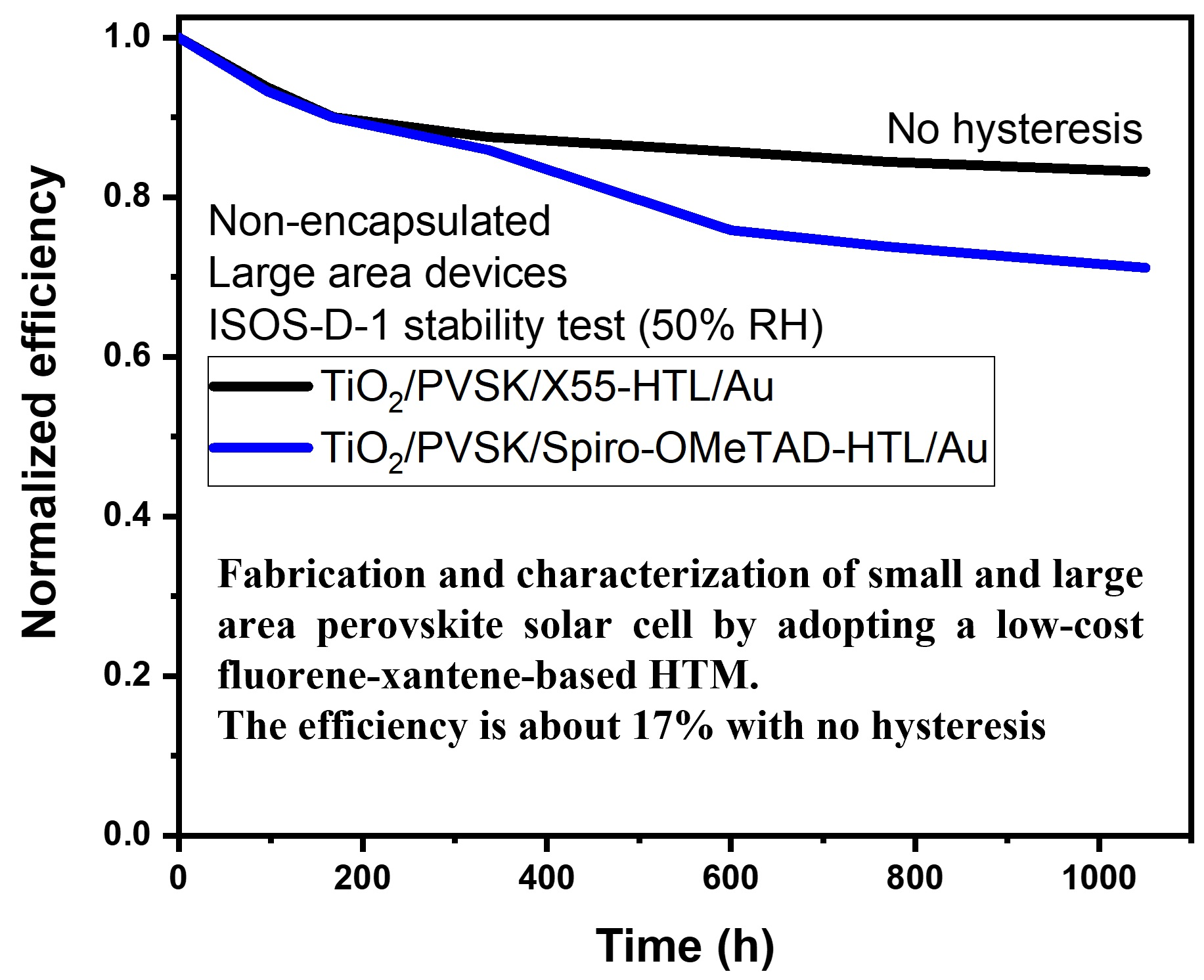
The experimentation was conducted on small (0.09 cm2) and large area (1.01 cm2) cells (Figure 1b,c). In both cases we used the n-i-p structure with a mesoporous TiO2 (mp-TiO2) scaffold layer (Figure 1a).
The process is in a glove box environment except for compact TiO2 (c-TiO2) and mp-TiO2 deposition; 2.5 × 2.5 cm2 FTO (fluorinated tin oxide)-covered glasses (Pilkington, 7 Ω/sq.) are cleaned with a soap/water solution and then in an ultrasonic bath with acetone, ethanol and 2-propanol for 10 min each. A 40 nm thick c-TiO2 layer is deposited by spray pyrolysis technique at 450 °C. Then, the mp-TiO2 paste (30 nrd, Great Cell Solar) diluted with ethanol (1:5 w/w) is spin coated and sintered at 480 °C for 30 min in a static furnace, forming the ETL. The substrate is then treated under a UV lamp to improve the substrate wettability prior to the perovskite deposition. The triple cation perovskite (Cs0.05(MA0.17FA0.83)0.95Pb(I0.83Br0.17)3 in DMF/DMSO, 1.42 M) (lead iodide from TCI Co., Ltd. (Tokyo, Japan); CsI, FAI and MABr from Great Cell Solar) is deposited by spin-coating technique in an N2-filled glove box environment. The precursor solution and then chlorobenzene are spun onto the substrate. The spin-coating parameters are 1000 rpm, 5 s ramp up, 10 s, then 5000 rpm, 2 s ramp up, 30 s. Then, we add chlorobenzene for 7 s before ending for both small and large area devices. After spin coating, the perovskite is annealed at 100 °C for 60 min. Spiro-OMeTAD (Borum, Hadsten, Denmark) and X55 (Dyenamo, Stockholm, Sweden) solutions are in chlorobenzene (73.52 and 70 mg/mL) doped with TBP (26.77 µL for both), Co salt (7.2 µL from a stock solution of 376 mg/mL in ACN) and Li-TFSI (16.66 and 16.61 µL from a stock solution of 520 mg/mL in ACN). Both the HTMs are spin coated (3000 rpm, 2 s ramp up, 30 s) in the glove box environment atop the perovskite forming the HTL. Following this, 80 nm-thick gold counter-electrode is thermally evaporated. The morphological analysis is realized with a field emission scanning electron microscope (Zeiss Auriga, Oberkochen, Germany). PL and IPCE measurement systems (Arkeo) are from Cicci Research. The photovoltaic characteristics and the MPP tracking are measured with a class A sun simulator (Sun 2000, Abet) at AM 1.5 1000 W/m2 calibrated with an SKS 1110 sensor (Skye Instruments Ltd., Llandrindod Wells, UK); the system is equipped with a 2612 source meter (Keithley Instruments Inc., Cleveland, OH, USA) and a LabVIEW interface.
3. Results and Discussion
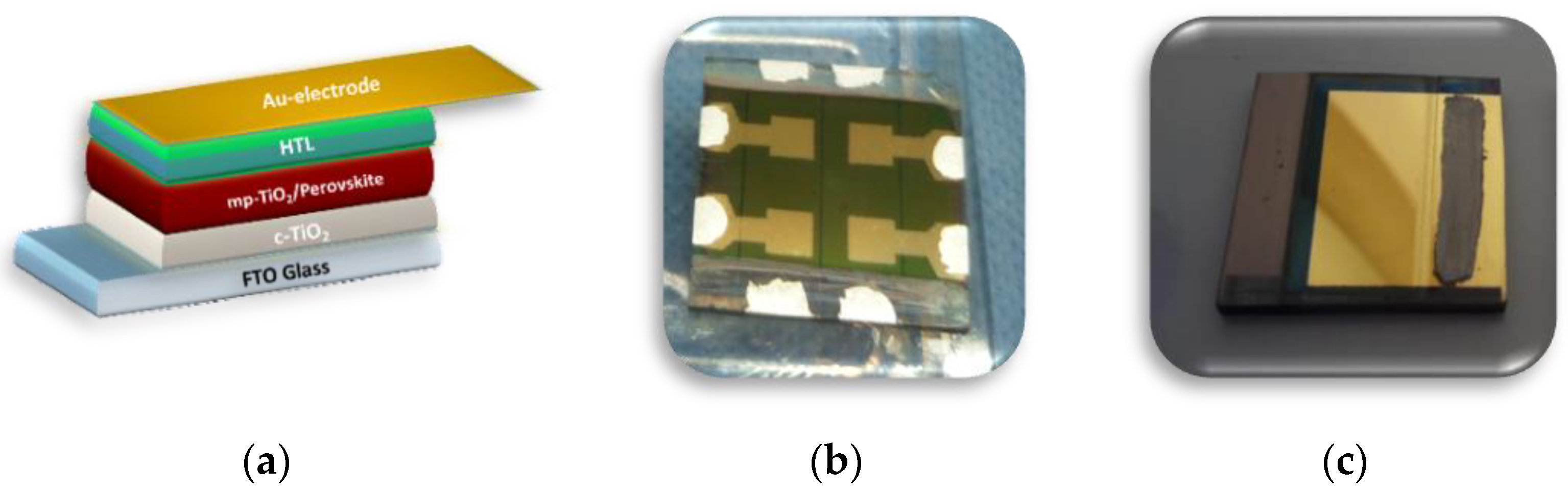
In Table 1 and Figure 2a, we show the statistics of 16 small area cells for each HTM and the J–V curves from the best-performing cells, respectively.
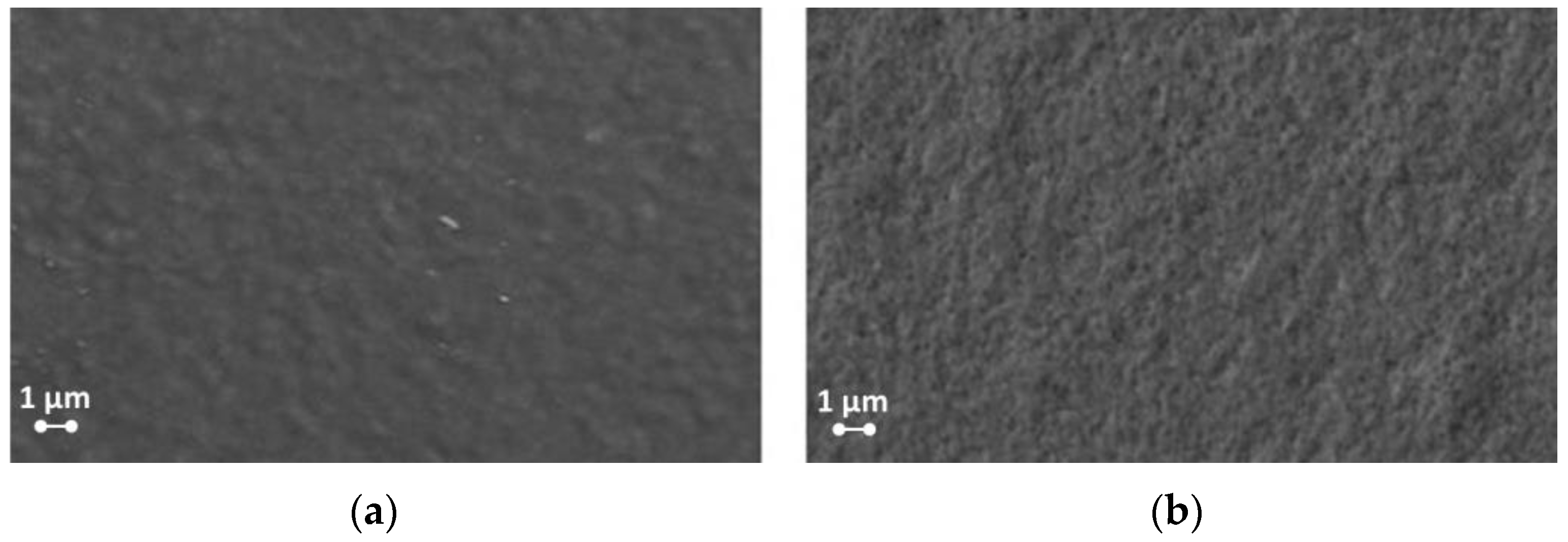
Both HTMs devices (Figure 2b) show low hysteresis index (HI = 1.02, defined as the relationship between the reverse and forward scan efficiencies [26]); however, X55-based cells have a higher Jsc with respect to Spiro-OMeTAD (21.46 vs. 20.18 mA/cm2) and consequently a higher efficiency (17% vs. 16.2%). The measured Jsc is in accordance with the integrated Jsc from the IPCE (incident photon to current efficiency) spectra (Figure 2c). The performance discrepancy between X55 and Spiro-OMeTAD HTM is mainly related to the better uniform surface coverage of the perovskite layer by X55 with respect to the Spiro-OMeTAD, where pinholes are clearly observed (Figure 3). The reduction of pinholes can limit the charge recombination losses at the perovskite/HTM interface.
The effective perovskite coverage by X55 is related to the good film-forming ability because of the presence of three SFX (spiro[fluorene-9,90-xanthene]) units in the molecular structure, which grants an optimal 3D geometry of the molecule that is able to make a uniform film above the absorber material. Concerning this, Bo et al. reported the absorption and photoluminescence (PL) spectra of X55 and Spiro-OMeTAD in toluene [17]. The three SFX units involve a larger conjugated system of X55 with respect to Spiro-OMeTAD, which causes the red shift of the X55 emission band. X55 and Spiro-OMeTAD have an absorption band in the visible (peak at 406 nm) and UV (peak at 388 nm) light region, respectively. In both cases the emission bands are red shifted. As reported in literature, the charge recombination loss reduction improves the charge collection efficiency and device performance (Figure 2) [17]. The steady state PL helps explain the hole transfer process at the perovskite-HTM interface and the higher current density with X55 HTM with respect to Spiro-OMeTAD HTM. HTM/PVSK combination lowers PL intensity with respect to the PVSK layer [27]. The interfacial hole transfer between X55 and PVSK is higher with respect to Spiro-OMeTAD and PVSK, because of the PL quenching (i.e., the PL intensity is lower than in the second case) (Figure 4).
The recombinations reduction can be well explained by analyzing the energy level alignment between the perovskite and the HTL. The HOMO energy levels of X55 and Spiro-OMeTAD are 5.23 and 5.13 eV, respectively [17,28]. In this condition and considering the valence band of the triple-cation perovskite used [29,30], both HTMs can extract the charge from the perovskite material, but the hole injection is favored in the X55 case because the hole contact is related to the HOMO level—X55-based devices exhibit higher Voc with respect to Spiro-OMeTAD-based cells (clearly visible in the following large area devices) [17,25,31].
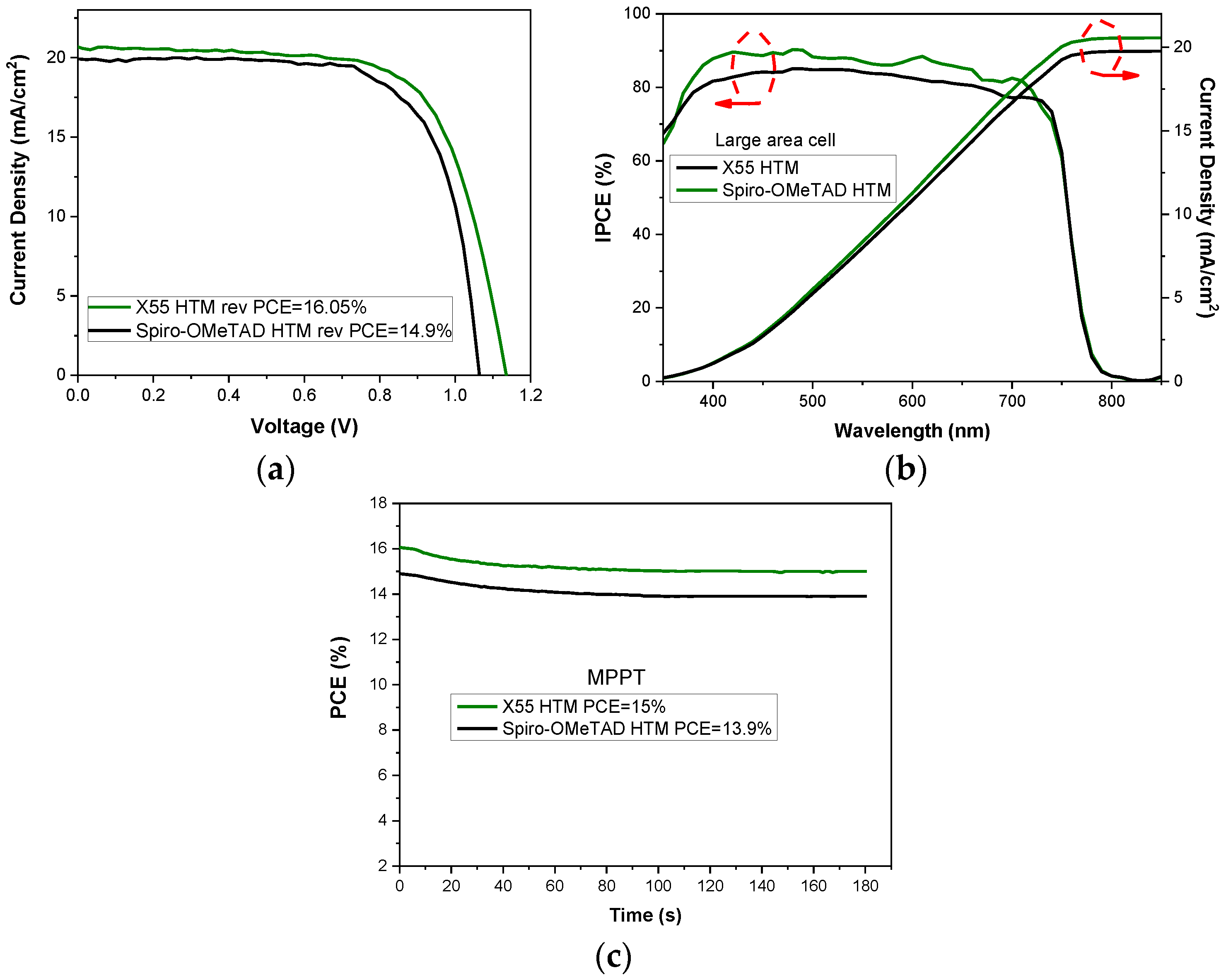
One of the key factors for further development of PVSK solar technology is the upscaling from a small area cell to module size [10,32]. The first step in this direction is the fabrication of a large area cell with a size greater than 1 cm2 [33]. We found an efficiency loss of about 5% by scaling to a large area size cell, mainly because of the fill factor (FF) (Table 2 and Figure 5a). This drop is mainly related to the front contact sheet resistance loss due to the increased area and diminished layer heterogeneity [32,34,35].
The current density is about 20 mA/cm2, as reported in the IPCE spectra (Figure 5b). The best efficiencies are 16.05% (15% stabilized at MPP) and 14.9% (13.9% stabilized at MPP) for the X55- and Spiro-OMeTAD-based devices, respectively (Figure 5a,c). As can be noticed, the performance gap between the two HTMs is higher in the large area (8%) than in the small area cells (5%). The better film-forming properties of X55 devices also show a higher VOC because of low defects and pin holes.
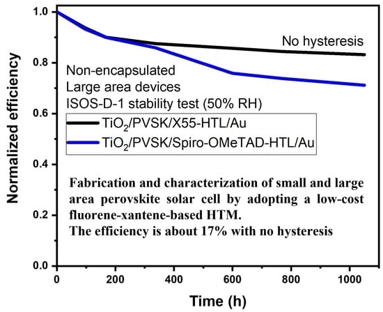
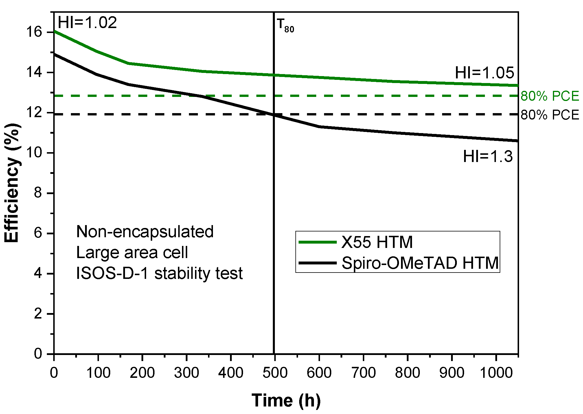
The commercialization of a photovoltaic technology is possible only if it is stable during the lifetime [9,36]. In literature, small area devices with X55 HTM were tested at room temperature (RT) and 20% humidity. Here, we checked the stability (Figure 6) of nonencapsulated large area devices for more than 1000 h in an ambient condition (ISOS-D-1, relative humidity of around 50%) [37].
After 1000 h, the efficiency drop is less than 15% for the X55 HTM and more than 30% for the Spiro-OMeTAD HTM. Moreover, the X55-based cell has no HI change during the test (from 1.02 to 1.05), while cells with Spiro-OMeTAD experience a large variation of the hysteresis cell between the beginning (HI = 1.02) and the end (HI = 1.3) of the test. Analyzing the shape of the curves [38], we estimate a T80 of 497 h for the reference case (PCE = 10.6%); X55 HTM is still above 80% of PCE (13.35%) after 1000 h. The high uniformity and homogeneity and the low recombination rate of the X55 HTL are the main causes of the better stability with respect to the reference case [17]. Furthermore, the two methoxy groups in the X55 structure have a higher hydrophobicity feature relative to the Spiro-OMeTAD HTM. Consequently, the moisture presence does not have a detrimental effect on the device performance.
4. Conclusions
The HTL plays a crucial role in terms of efficiency, stability and cost of PSCs. Devices based on the expensive Spiro-OMeTAD HTM have very high efficiency but poor stability in presence of humidity. In this work, we experimented with the cost-effective X55 HTM, which has a much deeper HOMO level and a higher hole mobility and conductivity than Spiro-OMeTAD. The results show a higher efficiency (17% vs. 16%), film homogeneity and better hole transport for the X55 with respect to the reference Spiro-OMeTAD. Then, we tested and publish for the first time the promising X55 HTM on large area devices during MPP tracking and under ISOS-D-1 stability test for more than 1000 h. On large area cells, the best efficiency is 16.05% and 14.9% for X55 and Spiro-OMeTAD HTM, respectively. We then found a stabilized efficiency at MPP of 15% for X55 and 13.9% for Spiro-OMeTAD. The efficiency drop was about 15% and 30% for the X55- and Spiro-OMeTAD-based device after 1000 h at ISOS-D-1 condition, respectively. The sturdiness relative to the moisture and the low upscaling losses make the X55 HTM a potential candidate for stable large area modules.
Author Contributions
Conceptualization, L.V., M.S. and A.D.C.; methodology, L.V. and M.S.; validation, L.V., M.S. and A.D.C.; formal analysis, L.V. and M.S.; investigation, L.V. and M.S.; resources, A.D.C.; data curation, L.V. and M.S.; writing—original draft preparation, L.V.; writing—review and editing, L.V., M.S. and A.D.C.; visualization, L.V. and M.S.; supervision, A.D.C. and L.V.; project administration, A.D.C. and L.V.; funding acquisition, A.D.C. All authors have read and agreed to the published version of the manuscript.
Funding
This research was funded by the European Union’s Horizon 2020 Framework Program for Funding and Research and Innovation under Grant Agreement no. 764047 (ESPResSo).
Data Availability Statement
The data presented in this study are available on request from the corresponding authors.
Acknowledgments
Authors would like to thank Francesco Mura from Sapienza University of Rome for support in SEM imaging.
Conflicts of Interest
The authors declare no conflict of interest.
References
- Green, M.A.; Dunlop, E.D.; Hohl-Ebinger, J.; Yoshita, M.; Kopidakis, N.; Hao, X. Solar cell efficiency tables (version 56). Prog. Photovolt. Res. Appl. 2020, 28, 629–638. [Google Scholar] [CrossRef]
- Kojima, A.; Teshima, K.; Shirai, Y.; Miyasaka, T. Organometal halide perovskites as visible-light sensitizers for photovoltaic cells. J. Am. Chem. Soc. 2009, 131, 6050–6051. [Google Scholar] [CrossRef]
- Kim, H.S.; Lee, C.R.; Im, J.H.; Lee, K.B.; Moehl, T.; Marchioro, A.; Moon, S.J.; Humphry-Baker, R.; Yum, J.H.; Moser, J.E.; et al. Lead iodide perovskite sensitized all-solid-state submicron thin film mesoscopic solar cell with efficiency exceeding 9%. Sci. Rep. 2012, 2, 591. [Google Scholar] [CrossRef] [PubMed] [Green Version]
- Brittman, S.; Adhyaksa, G.W.P.; Garnett, E.C. The expanding world of hybrid perovskites: Materials properties and emerging applications. MRS Commun. 2015, 5, 7–26. [Google Scholar] [CrossRef] [PubMed] [Green Version]
- Ahmed, M.I.; Habib, A.; Javaid, S.S. Perovskite Solar Cells: Potentials, Challenges, and Opportunities Muhammad. Int. J. Photoenergy 2015, 2015, 592308. [Google Scholar] [CrossRef] [Green Version]
- Nayak, P.K.; Mahesh, S.; Snaith, H.J.; Cahen, D. Photovoltaic solar cell technologies: Analysing the state of the art. Nat. Rev. Mater. 2019, 4, 269–285. [Google Scholar] [CrossRef]
- Snaith, H.J. Present status and future prospects of perovskite photovoltaics. Nat. Mater. 2018, 17, 372–376. [Google Scholar] [CrossRef]
- Parisi, M.L.; Maranghi, S.; Vesce, L.; Sinicropi, A.; Di Carlo, A.; Basosi, R. Prospective life cycle assessment of third-generation photovoltaics at the pre-industrial scale: A long-term scenario approach. Renew. Sustain. Energy Rev. 2020, 121, 109703. [Google Scholar] [CrossRef]
- Vesce, L.; Guidobaldi, A.; Mariani, P.; Carlo, A.D.I.; Parisi, M.L.; Maranghi, S.; Basosi, R. Scaling-up of Dye Sensitized Solar Modules. In World Scientific Reference of Hybrid Materials; World Scientific: Singapore, 2018; Volume 2. [Google Scholar] [CrossRef]
- Vesce, L.; Stefanelli, M.; Herterich, J.P.; Castriotta, L.A.; Kohlstädt, M.; Würfel, U.; Di Carlo, A. Ambient Air Blade-coating Fabrication of Stable Triple Cation Perovskite Solar Modules by Green Solvent Quenching. Sol. RRL 2021, 5, 2100073. [Google Scholar] [CrossRef]
- Matteocci, F.; Vesce, L.; Kosasih, F.U.; Castriotta, L.A.; Cacovich, S.; Palma, A.L.; Divitini, G.; Ducati, C.; Di Carlo, A. Fabrication and Morphological Characterization of High-Efficiency Blade-Coated Perovskite Solar Modules. ACS Appl. Mater. Interfaces 2019, 11, 25195–25204. [Google Scholar] [CrossRef]
- Mincuzzi, G.; Vesce, L.; Liberatore, M.; Reale, A.; Di Carlo, A.; Brown, T.M. Laser-sintered TiO2 films for dye solar cell fabrication: An electrical, morphological, and electron lifetime investigation. IEEE Trans. Electron Devices 2011, 58, 3179–3188. [Google Scholar] [CrossRef]
- Rong, Y.; Hu, Y.; Mei, A.; Tan, H.; Saidaminov, M.I.; Seok, S.I.; McGehee, M.D.; Sargent, E.H.; Han, H. Challenges for commercializing perovskite solar cells. Science 2018, 361, eaat8235. [Google Scholar] [CrossRef] [Green Version]
- Shi, Z.; Jayatissa, A.H. Perovskites-based solar cells: A review of recent progress, materials and processing methods. Materials 2018, 11, 729. [Google Scholar] [CrossRef] [Green Version]
- Barichello, J.; Vesce, L.; Matteocci, F.; Lamanna, E.; Di Carlo, A. The effect of water in Carbon-Perovskite Solar Cells with optimized alumina spacer. Sol. Energy Mater. Sol. Cells 2019, 197, 76–83. [Google Scholar] [CrossRef]
- Caliό, L.; Kazim, S.; Grätzel, M.; Ahmad, S. Hole-transport materials for perovskite solar cells. Angew. Chem. Int. Ed. 2016, 55, 14522–14545. [Google Scholar] [CrossRef]
- Xu, B.; Zhang, J.; Hagfeldt, A.; Jen, K.; Sun, L.; Xu, B.; Zhang, J.; Hua, Y.; Liu, P.; Wang, L.; et al. Tailor-Making Low-Cost Spiro[fluorene-9,90-xanthene]-Based 3D Oligomers for Perovskite Solar Cells Tailor-Making Low-Cost 3D Oligomers for Perovskite Solar Cells. Chem 2017, 54, 676–687. [Google Scholar] [CrossRef] [Green Version]
- Swetha, T.; Singh, S.P. Perovskite solar cells based on small molecule hole transporting materials. J. Mater. Chem. A 2015, 2, 18329–18344. [Google Scholar] [CrossRef]
- Madhaven, V.E.; Zimmermann, I.; Carmona, C.R.; Grancini, G.; Buffiere, M.; Belaidi, A.; Nazeeruddin, M.K. Copper thiocyanate inorganic hole-transporting material for high-efficiency PSCs. ACS Energy Lett. 2016, 1, 1112–1117. [Google Scholar] [CrossRef]
- Hendriks, K.H.; Van Franeker, J.J.; Bruijnaers, B.J.; Anta, J.A.; Wienk, M.M.; Janssen, R.A.J. 2-Methoxyethanol as a new solvent for processing methylammonium lead halide PSCs. J. Mater. Chem. A 2017, 2346–2354. [Google Scholar] [CrossRef]
- Yin, X.; Chen, P.; Que, M.; Xing, Y.; Que, W.; Niu, C.; Shao, J. Highly efficient flexible PSCs using solution-derived NiOx hole contacts. ACS Nano 2016, 19, 3630–3636. [Google Scholar] [CrossRef]
- Heo, J.H.; Im, S.H.; Noh, J.H.; Mandal, T.N.; Lim, C.S.; Chang, J.A.; Lee, Y.H.; Kim, H.J.; Sarkar, A.; Nazeeruddin, M.K.; et al. Efficient inorganic-organic hybrid heterojunction solar cells containing perovskite compound and polymeric hole conductors. Nat. Photon. 2013, 7, 487–492. [Google Scholar] [CrossRef]
- Desoky, M.M.H.; Bonomo, M.; Buscaino, R.; Fin, A.; Viscardi, G.; Barolo, C.; Quagliotto, P. Dopant-Free All-Organic Small-Molecule HTMs for Perovskite Solar Cells: Concepts and Structure—Property Relationships. Energies 2021, 14, 2279. [Google Scholar] [CrossRef]
- Rakstys, K.; Paek, S.; Sohail, M.; Gao, P.; Cho, K.T.; Gratia, P.; Lee, Y.; Dahmen, K.H.; Nazeeruddin, M.K. Highly hindered bithiophene-functionalized dispiro-oxepine derivative as efficient hole transporting material for perovskite solar cells. J. Mater. Chem. A 2016, 4, 18259–18264. [Google Scholar] [CrossRef]
- Xu, B.; Bi, D.; Hua, Y.; Liu, P.; Cheng, M.; Grätzel, M.; Kloo, L.; Hagfeldt, A.; Sun, L. A low-cost spiro[fluorene-9,9′-xanthene]-based hole transport material for highly efficient solid-state dye-sensitized solar cells and perovskite solar cells. Energy Environ. Sci. 2016, 9, 873–877. [Google Scholar] [CrossRef]
- Habisreutinger, S.N.; Noel, N.K.; Snaith, H.J. Hysteresis Index: A Figure without Merit for Quantifying Hysteresis in Perovskite Solar Cells. ACS Energy Lett. 2018, 3, 2472–2476. [Google Scholar] [CrossRef] [Green Version]
- Wu, J.; Liu, C.; Hu, M.; Deng, X.; Tan, W.; Tian, Y.; Xu, B. Polystyrene with a methoxytriphenylamine-conjugated-thiophene moiety side-chain as a dopant-free hole-transporting material for perovskite solar cells. J. Mater. Chem. A 2018, 6, 13123–13132. [Google Scholar] [CrossRef]
- Dyenamo Website. Available online: www.dyenamo.se/dyenamo_hole_transport_materials.php (accessed on 10 September 2021).
- Saliba, M.; Matsui, T.; Seo, J.Y.; Domanski, K.; Correa-Baena, J.P.; Nazeeruddin, M.K.; Zakeeruddin, S.M.; Tress, W.; Abate, A.; Hagfeldt, A.; et al. Cesium-containing triple cation perovskite solar cells: Improved stability, reproducibility and high efficiency. Energy Environ. Sci. 2016, 9, 1989–1997. [Google Scholar] [CrossRef] [PubMed] [Green Version]
- Deepa, M.; Salado, M.; Calio, L.; Kazim, S.; Shivaprasad, S.M.; Ahmad, S. Cesium power: Low Cs+ levels impart stability to perovskite solar cells. Phys. Chem. Chem. Phys. 2017, 19, 4069–4077. [Google Scholar] [CrossRef]
- Gelmetti, I.; Montcada, N.F.; Pérez-Rodriguez, A.; Barrena, E.; Ocal, C.; Garcia-Benito, I.; Molina-Ontoria, A.; Martin, N.; Vidal-Ferran, A.; Palomares, E. Energy Alignment and Recombination in Perovskite Solar Cells: Weighted Influence on the Open Circuit Voltage. Energy Environ. Sci. 2019, 12, 1309–1316. [Google Scholar] [CrossRef]
- Yang, Z.; Chueh, C.C.; Zuo, F.; Kim, J.H.; Liang, P.W.; Jen, A.K.Y. High-Performance Fully Printable Perovskite Solar Cells via Blade-Coating Technique under the Ambient Condition. Adv. Energy Mater. 2015, 5, 1500328. [Google Scholar] [CrossRef]
- Castriotta, L.A.; Matteocci, F.; Vesce, L.; Cinà, L.; Agresti, A.; Pescetelli, S.; Ronconi, A.; Löffler, M.; Stylianakis, M.M.; Di Giacomo, F.; et al. Air-Processed Infrared-Annealed Printed Methylammonium-Free Perovskite Solar Cells and Modules Incorporating Potassium-Doped Graphene Oxide as an Interlayer. ACS Appl. Mater. Interfaces 2021, 13, 11741–11754. [Google Scholar] [CrossRef] [PubMed]
- Li, Z.; Klein, T.R.; Kim, D.H.; Yang, M.; Berry, J.J.; Van Hest, M.F.A.M.; Zhu, K. Scalable fabrication of perovskite solar cells. Nat. Rev. Mater. 2018, 3, 18017. [Google Scholar] [CrossRef]
- Vesce, L.; Stefanelli, M.; Carlo, A. Di Low temperature process of homogeneous and pin-hole free Perovskite layers for fully coated photovoltaic devices up to 256 cm 2 area at ambient condition. In Proceedings of the 2019 International Symposium on Advanced Electrical and Communication Technologies (ISAECT), Rome, Italy, 27–29 November 2019; pp. 1–5. [Google Scholar]
- Castro-Hermosa, S.; Yadav, S.K.; Vesce, L.; Guidobaldi, A.; Reale, A.; Di Carlo, A.; Brown, T.M. Stability issues pertaining large area perovskite and dye-sensitized solar cells and modules. J. Phys. D. Appl. Phys. 2017, 50, 33001. [Google Scholar] [CrossRef]
- Kumar, P.; Bilen, C.; Vaughan, B.; Zhou, X.; Dastoor, P.C.; Belcher, W.J. Comparing the degradation of organic photovoltaic devices under ISOS testing protocols. Sol. Energy Mater. Sol. Cells 2016, 149, 179–186. [Google Scholar] [CrossRef]
- Domanski, K.; Alharbi, E.A.; Hagfeldt, A.; Grätzel, M.; Tress, W. Systematic investigation of the impact of operation conditions on the degradation behaviour of perovskite solar cells. Nat. Energy 2018, 3, 61–67. [Google Scholar] [CrossRef]
Figure 1.
(a) Perovskite solar cell full stack: (b) four small area (0.09 cm2) cells and (c) one large area (1.01 cm2) cell on 2.5 × 2.5 cm2 substrates.
Figure 1.
(a) Perovskite solar cell full stack: (b) four small area (0.09 cm2) cells and (c) one large area (1.01 cm2) cell on 2.5 × 2.5 cm2 substrates.

Figure 2.
(a) Efficiency statistics of the fabricated small area cells (0.09 cm2). (b) JV curves of the best small area cells and (c) corresponding incident photon to current efficiency (IPCE).
Figure 2.
(a) Efficiency statistics of the fabricated small area cells (0.09 cm2). (b) JV curves of the best small area cells and (c) corresponding incident photon to current efficiency (IPCE).

Figure 3.
(a) SEM images of X55 and (b) Spiro-OMeTAD HTLs.

Figure 4.
Perovskite layer and perovskite/HTL photoluminescence.

Figure 5.
(a) JV curves of the best large area cells and (b) corresponding IPCE. (c) MPP tracking.

Figure 6.
Efficiency trend according to ISOS-D-1 standard (relative humidity of around 50%) of nonencapsulated large area devices.
Figure 6.
Efficiency trend according to ISOS-D-1 standard (relative humidity of around 50%) of nonencapsulated large area devices.


Table 1.
Statistics of the fabricated small area cells: 16 with X55 HTM and 16 with Spiro-OMeTAD HTM.
Table 1.
Statistics of the fabricated small area cells: 16 with X55 HTM and 16 with Spiro-OMeTAD HTM.
| Electrical Parameters | X55-Based Devices | Spiro-OMeTAD-Based Devices |
|---|---|---|
| VOC (V) | 1.07 ± 0.04 | 1.05 ± 0.04 |
| JSC (mA/cm2) | 21.15 ± 0.31 | 19.98 ± 0.20 |
| FF (%) | 70.15 ± 1.03 | 72.43 ± 1.15 |
| PCE (%) | 16.7 ± 0.30 | 15.88 ± 0.32 |
Table 2.
Statistics of the fabricated large area cells: 16 with X55 HTM and 16 with Spiro-OMeTAD HTM.
Table 2.
Statistics of the fabricated large area cells: 16 with X55 HTM and 16 with Spiro-OMeTAD HTM.
| Electrical Parameters | X55-Cased Devices | Spiro-OMeTAD-Based Devices |
| VOC (V) | 1.08 ± 0.05 | 1.01 ± 0.05 |
| JSC (mA/cm2) | 20.26 ± 0.40 | 19.98 ± 0.20 |
| FF (%) | 67.57 ± 1.20 | 70.09 ± 1.10 |
| PCE (%) | 15.65 ± 0.40 | 14.49 ± 0.41 |
Publisher’s Note: MDPI stays neutral with regard to jurisdictional claims in published maps and institutional affiliations. |
© 2021 by the authors. Licensee MDPI, Basel, Switzerland. This article is an open access article distributed under the terms and conditions of the Creative Commons Attribution (CC BY) license (https://creativecommons.org/licenses/by/4.0/).
Share and Cite
MDPI and ACS Style
Vesce, L.; Stefanelli, M.; Di Carlo, A. Efficient and Stable Perovskite Large Area Cells by Low-Cost Fluorene-Xantene-Based Hole Transporting Layer. Energies 2021, 14, 6081. https://doi.org/10.3390/en14196081
AMA Style
Vesce L, Stefanelli M, Di Carlo A. Efficient and Stable Perovskite Large Area Cells by Low-Cost Fluorene-Xantene-Based Hole Transporting Layer. Energies. 2021; 14(19):6081. https://doi.org/10.3390/en14196081
Chicago/Turabian StyleVesce, Luigi, Maurizio Stefanelli, and Aldo Di Carlo. 2021. "Efficient and Stable Perovskite Large Area Cells by Low-Cost Fluorene-Xantene-Based Hole Transporting Layer" Energies 14, no. 19: 6081. https://doi.org/10.3390/en14196081
Note that from the first issue of 2016, this journal uses article numbers instead of page numbers. See further details here.