Rediscovering Majority Logic in the Post-CMOS Era: A Perspective from In-Memory Computing


Chair of Computer Science 3—Computer Architecture, Friedrich-Alexander-Universität Erlangen-Nürnberg (FAU), 91058 Erlangen, Germany
J. Low Power Electron. Appl. 2020, 10(3), 28; https://doi.org/10.3390/jlpea10030028
Submission received: 5 August 2020
/
Revised: 25 August 2020
/
Accepted: 2 September 2020
/
Published: 4 September 2020
(This article belongs to the Special Issue Low Power Memory/Memristor Devices and Systems)
Abstract
:As we approach the end of Moore’s law, many alternative devices are being explored to satisfy the performance requirements of modern integrated circuits. At the same time, the movement of data between processing and memory units in contemporary computing systems (‘von Neumann bottleneck’ or ‘memory wall’) necessitates a paradigm shift in the way data is processed. Emerging resistance switching memories (memristors) show promising signs to overcome the ‘memory wall’ by enabling computation in the memory array. Majority logic is a type of Boolean logic which has been found to be an efficient logic primitive due to its expressive power. In this review, the efficiency of majority logic is analyzed from the perspective of in-memory computing. Recently reported methods to implement majority gate in Resistive RAM array are reviewed and compared. Conventional CMOS implementation accommodated heterogeneity of logic gates (NAND, NOR, XOR) while in-memory implementation usually accommodates homogeneity of gates (only IMPLY or only NAND or only MAJORITY). In view of this, memristive logic families which can implement MAJORITY gate and NOT (to make it functionally complete) are to be favored for in-memory computing. One-bit full adders implemented in memory array using different logic primitives are compared and the efficiency of majority-based implementation is underscored. To investigate if the efficiency of majority-based implementation extends to n-bit adders, eight-bit adders implemented in memory array using different logic primitives are compared. Parallel-prefix adders implemented in majority logic can reduce latency of in-memory adders by 50–70% when compared to IMPLY, NAND, NOR and other similar logic primitives.
1. Introduction
Extraordinary innovation in the field of Integrated circuits is the last 50 years was based on Moore’s law scaling and predominantly the Complementary Metal Oxide Semiconductor (CMOS) technology. Whether we have reached the end of Moore’s law or approaching it in the near future (an issue being debated), it is evident that some signs are clear. The processor clock frequency, a key measure of performance has plateaued [1], the regular doubling of integration density has slowed down in 14 nm and 10 nm CMOS [2] and 2D lithography has reached its limits [3]. Beyond-CMOS research has been underway in the last decade to find an alternative device which is better than CMOS in its characteristics. This includes CMOS-like devices (tunnel FET, GaN TFET, Graphene ribbon pn junction, Ferroelectric FET) [4], quantum-dot cellular automata (QCA), nanomagnet logic, resistance-switching devices (Resistive RAM, Phase Change Memory, conductive bridge RAM), spin-based devices, and plasmonic-based devices [5]. Although some of these post-CMOS devices possessed valuable features like low-voltage operation and non-volatility, recent bench-marking efforts seem to suggest that none of these devices could outperform CMOS in the most critical aspects of computing (energy, latency and area) [4,6]. Hence it is envisaged that post-CMOS devices will augment and enhance CMOS-based computational fabrics and will not completely replace CMOS technology.
Majority logic, a type of Boolean logic, is defined to be true if more than half of the n inputs are true, where n is odd. Hence, a majority gate is a democratic gate and, it can be expressed in terms of Boolean AND/OR as , where are Boolean variables. Although majority logic was known since 1960, there has been a rediscovery in using it for computation in many post-CMOS devices. A majority gate based on spin waves [7], Quantum-Dot cellular automata [8], nano magnetic logic [9], and Single Electron Tunneling [10] have been demonstrated and in some of these technologies, it is more efficient to implement a majority gate [11] than other other logic primitives (NAND, NOR, XOR). Recent research [6,12,13,14] has confirmed that majority logic is to be preferred not only because a particular nanotechnology can realize it, but also because of its ability to implement arithmetic-intensive circuits with less gates, i.e., in a compact manner. For arithmetic intensive benchmarks, it has been proved that Majority-Invert Graphs (MIGs) can achieve up to 33% reduction in logical depth compared to And-Invert Graphs (AIGs) produced by Berkeley’s ABC synthesis tool [12]. Such findings from research in logic synthesis implies that circuits implemented using majority logic will be better regardless of the post-CMOS device used. In this review, we limit our discussion to how majority logic could be implemented using RRAM technology since in-memory computing is the focus of this review. A review of how a majority gate could be implemented using other post-CMOS devices is presented in [15,16].
The movement of data between processing and memory units is the major cause for the degraded performance of contemporary computing systems, often referred to as the ‘von Neumann bottleneck’ or ‘memory wall’ [17,18]. ‘Computation energy’ is dominated by ‘data movement energy’ since the energy for memory access grows exponentially along the memory hierarchy (from cache to off-chip DRAM). There has been an ongoing effort (for 10-15 years) to combat the memory wall by bringing the processor and memory unit closer to each other. Resistive RAMs are two terminal devices (usually a Metal-Insulator-Metal structure [19]) capable of storing data as resistance. Although RRAM (memristor) was initially experimented as a non-volatile memory technology, it was later discovered that certain Boolean logic operations (IMPLY logic [20,21] and NOR [22] were the first logic gates that were explored) can be implemented in the memory array. Boolean gates were implemented by modifying the structure of the memory array or modifying the peripheral circuitry or a combination of these. In-memory computing (also called ‘processing-in-memory’) refers to any effort to process data at the residence of data (i.e., in the memory array) without moving it out to a separate processing unit. ‘Processing/computing’ could mean a wide variety of operations from arithmetic operations to cognitive tasks like machine learning and pattern recognition [23]. In this review, the focus is on arithmetic operations and how majority logic can enable efficient in-memory computing.
The rest of this review is structured as follows. In Section 2, we first give a brief overview on ‘memristive logic’, the methodology of designing logic circuits using memristors. This is followed by a discussion on how majority gate is implemented in RRAM array in Section 3. Three possible ways are discussed. In Section 4, we analyse the latency of in-memory one-bit adder using different logic primitives and highlight the latency reduction obtained by majority logic. To investigate if majority logic can be efficient for n-bit adders, 8-bit adders implemented using different logic primitives and different types (ripple carry, carry look-ahead, parallel-prefix) are analysed and compared, followed by conclusion in Section 6.
2. Memristive Logic
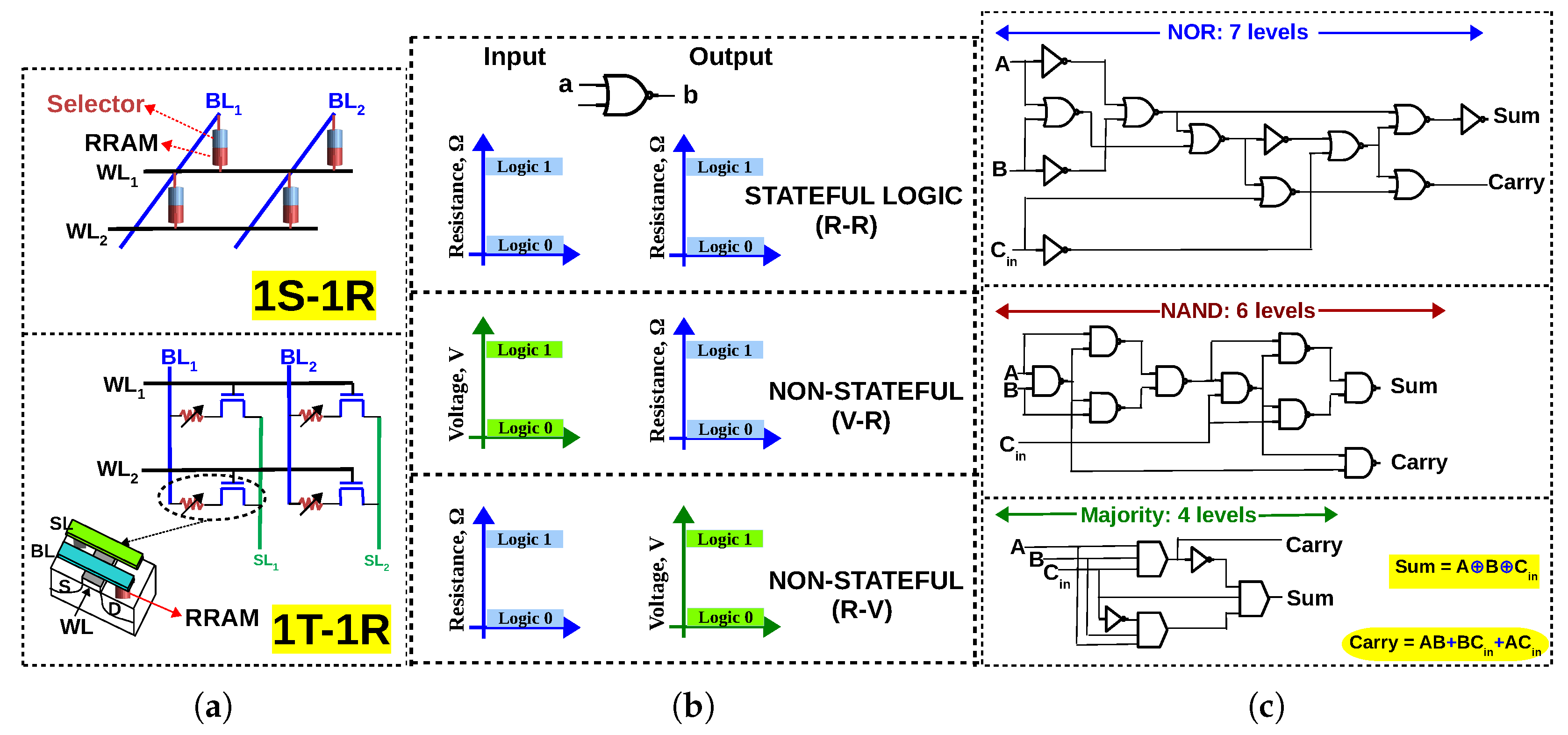
A short introduction to memristors and different array configurations of such non-volatile memories is appropriate before the introduction of memristive logic. Memristors are a class of emerging Non-Volatile Memories (NVMs) which store data as resistance. Under voltage/current stress, the resistance can be switched between a Low Resistance State (LRS) and a High Resistance State (HRS). The word ‘memristor’ is used because such a device is basically a ‘resistor’ with a ‘memory’. Depending on what causes the change in resistance, a memristor can be classified as follows: Resistive Random Access Memory (RRAM) where the change in resistance is due to the formation and rupture of a conductive filament [24]; Phase Change Memory (PCM) where the change in resistance is due to the amorphous or crystalline state of the chalcogenide phase-change material; Spin Transfer Torque-Magnetic RAM (STT-MRAM) where the change in resistance is due to the magnetic polarization. To construct a memory array using such devices, two configurations are common: 1Transistor-1 Resistor (1T–1R) and 1Selector-1 Resistor (1S–1R), as illustrated in Figure 1a. The 1T–1R configuration uses a transistor as an access device for each memory cell, allowing one to access a particular cell without interfering with its neighbours in the array [25,26]. The 1S–1R configuration uses a two-terminal device called a ‘selector’ which has a diode-like characteristic. The selector is assembled in series with the memristive device. Different types of selectors have been experimentally demonstrated in [27,28,29,30]. The 1S–1R is area-efficient, but suffers from sneak–path problem because it is not possible to program (read or write to a cell) a cell without interfering with its neighbours [22].
Memristive logic is the art of designing logic circuits using memristors [17,18]. Conventionally, arithmetic circuits have been implemented using logic gates built from CMOS transistors. In contrast, a memristive logic family formulates a ‘functionally complete’ Boolean logic using a memristive device (RRAM/PCM/STT-MRAM) as the primary switching device (CMOS circuitry may also be used, but in a peripheral manner). For example, NOR is ‘functionally complete’ since any Boolean logic can be expressed in terms of NOR gates. Therefore, if a NOR gate can be designed using memristive devices, any Boolean logic can be implemented using memristive devices. Furthermore, most researchers try to make their logic gates executable in an array configuration so that they can be exploited for in-memory computing. NAND, IMPLY+FALSE [35] and Majority+NOT [12] are also functionally complete. From the perspective of the state variable used for computation, memristive logic family can be classified as either stateful or non-stateful. A memristive logic family is said to be stateful if the Boolean variable is represented only as the internal state of the memristor (i.e., its resistance) and computation is performed by manipulating this state [36]. If voltage is also used in addition to resistance, the logic family is said to be non-stateful (Figure 1b). Some logic families are classified on this criteria in [18].
A characteristic of memristive logic families is that, with certain modifications to the conventional memory, a particular logic primitive can be implemented and, other logic primitives have to be realized in terms of that logic primitive. For example, in the NOR-based memristive family (MAGIC [31]), all other gates (AND, OR, XOR) have to be expressed in terms of NOR gates and then mapped to the memory array. It must be noted that even the NOR logic primitive is implemented with modifications to the peripheral circuitry of the conventional memory array, namely the row decoder (modified to bias the rows at ‘isolation voltage’ to prevent unintended NOR operation in those rows) and the WRITE circuitry (modified to apply the MAGIC execution voltage which is twice the WRITE voltage). Similarly, in the NAND-based logic family reported in [37], XOR gate is implemented as a sequence of four NAND operations. This implies that if the fundamental logic primitive of a memristive logic family is weak, all in-memory computation performed using that logic family will be in-efficient (requiring long sequences of operations). To illustrate, Figure 1c depicts a 1-bit full adder expressed in terms of a particular logic primitive (NOR/NAND/Majority), as required for in-memory implementation. For a 1-bit adder, majority logic (together with NOT gates) can achieve 33–43% reduction in logic levels compared to NAND/NOR, while for bigger circuits, this percentage may vary. Research in logic synthesis suggests that circuits synthesized in terms of majority and NOT gates (Majority-Invert-Graphs) can achieve up to 33% reduction in logical depth compared to And-Invert-Graphs (AIGs) for arithmetic intensive circuits [12]. It must be emphasized that for any memristive logic, the number of cycles/steps to execute a circuit in-memory will be larger than the number of logic levels, i.e, n levels of Boolean logic will require cycles in-memory, where x depends on the memristive logic family and its capability to execute gates in parallel. Therefore, it is evident that to reduce the latency of in-memory computing, the synthesized logic must be latency optimized (before mapping to CMOS or a post-CMOS device). Stronger logic primitives like majority can minimize latency and the purpose of this review is to highlight the efficiency of memristive logic family with majority as the fundamental logic primitive (complemented with NOT since majority as a sole logic primitive is functionally incomplete).
3. In-Memory Majority Logic
In literature, there are two viable ways in which a majority gate is implemented in Resistive RAM array. Both are non-stateful logic families. Following the naming convention introduced in [38] (‘input state variable-output state variable’ logic), a non-stateful logic family can be V–R logic (input state variable is voltage and the output is resistance) or R–V logic (input state variable is resistance and output is voltage), as illustrated in Figure 1b. In this section, the principle of implementing a in-memory majority gate in V–R and R–V logic is reviewed and the advantages and disadvantages are analysed. In addition to the aforementioned methods, a in-memory minority gate (inverse of majority gate) is also theoretically proposed in [39]. The minority gate is realized by exploiting voltage division between three RRAMs (which store the inputs) and an output RRAM. However, the correct functioning of such a gate is not guaranteed since recent research has shown that variability is intrinsic to RRAM technology and cannot be completely eradicated [40,41]. In the presence of variations (in RRAM’s switching voltages and resistive states), such a minority gate is not feasible in RRAM array, and hence it is not discussed in detail in this review.
3.1. V–R Majority Logic
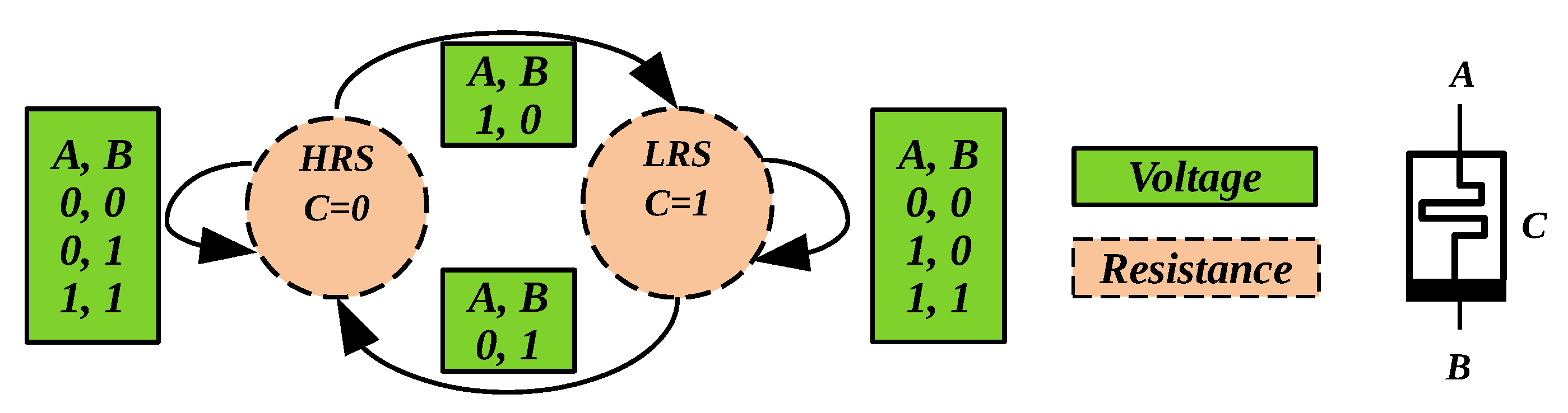
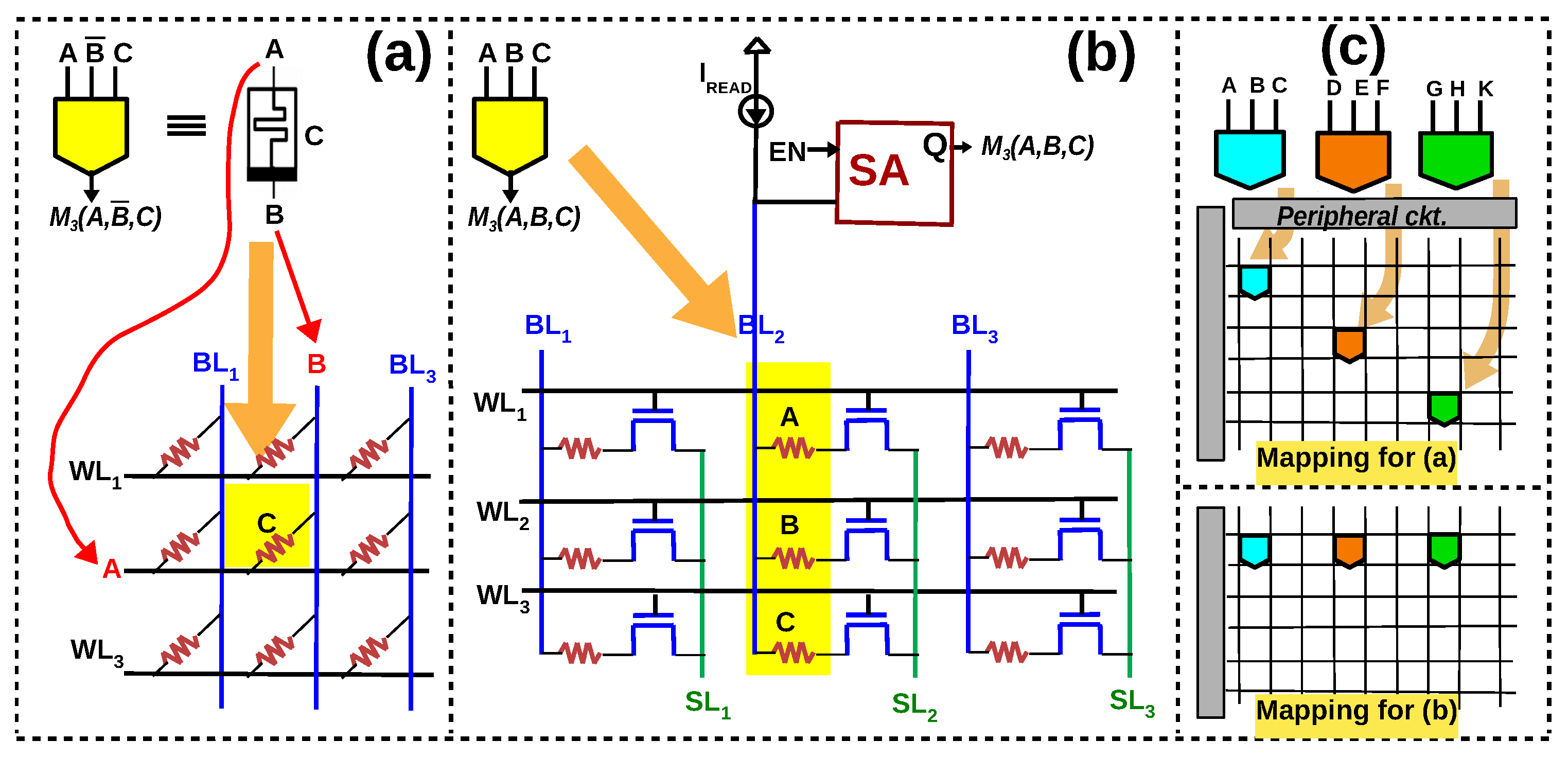
In [42,43,44], majority gate is implemented in RRAM array (1S–1R) by applying two inputs of the majority gate as voltages at and of the array (the third input being the initial state of the RRAM) and the output is the new non-volatile state of the device. Hence this way of implementing majority can be called V–R logic, though in the strict sense, it should be VandR–R logic since the third input is resistance (initial state of the RRAM). However, it can be justified to be simply called V–R logic since the output (switching of resistance) is triggered on the applications of voltages. The fourth column of Table 1 depicts , the 3-input majority function of the first three columns. Note that = . To understand how a Resistive RAM cell can implement the majority function, consider a situation in which the Boolean variable C of Table 1 is the initial state of a memory cell (following the convention used in this field, logic 0 is HRS and logic 1 is LRS). Let us assume that the RRAM cell holding C has a symmetric switching characteristic, i.e., its internal resistance value changes from HRS to LRS when a voltage is applied across its terminals and from LRS to HRS when - is applied. As in the CMOS realm, logic 1 is a high voltage, which we will fix as , and logic 0 corresponds to ground.
If A and B are applied across the two terminals of the RRAM cell, its state will either switch or remain the same in accordance with the initial state. Figure 2 illustrates the different combinations of (A, B, C) on a RRAM cell. When A is logic 1 and B is logic 0, the applied voltage across the RRAM cell is , triggering a transition from HRS to LRS and vice versa. When both A and B are (0,0) or (1,1), the state of the memristor will not change. This specific behavior can be captured as a new functionally complete Boolean function, called ‘Resistive Majority’, , which describes the new nonvolatile state of the cell as a function of an initial internal state C and the voltages A and B applied across the terminals of the device. Note that , as listed in Table 1. Complex functions can be easily expressed and manipulated as operators using Majority-Inverter Graphs (MIG), a recently introduced logic manipulation structure consisting of three input majority nodes and regular/complemented edges [12]. In [18], the authors elaborate how an eight-bit adder is expressed in MIGs and then mapped to the memristive memory array using the aforementioned resistive majority function.
3.2. R–V Majority Logic
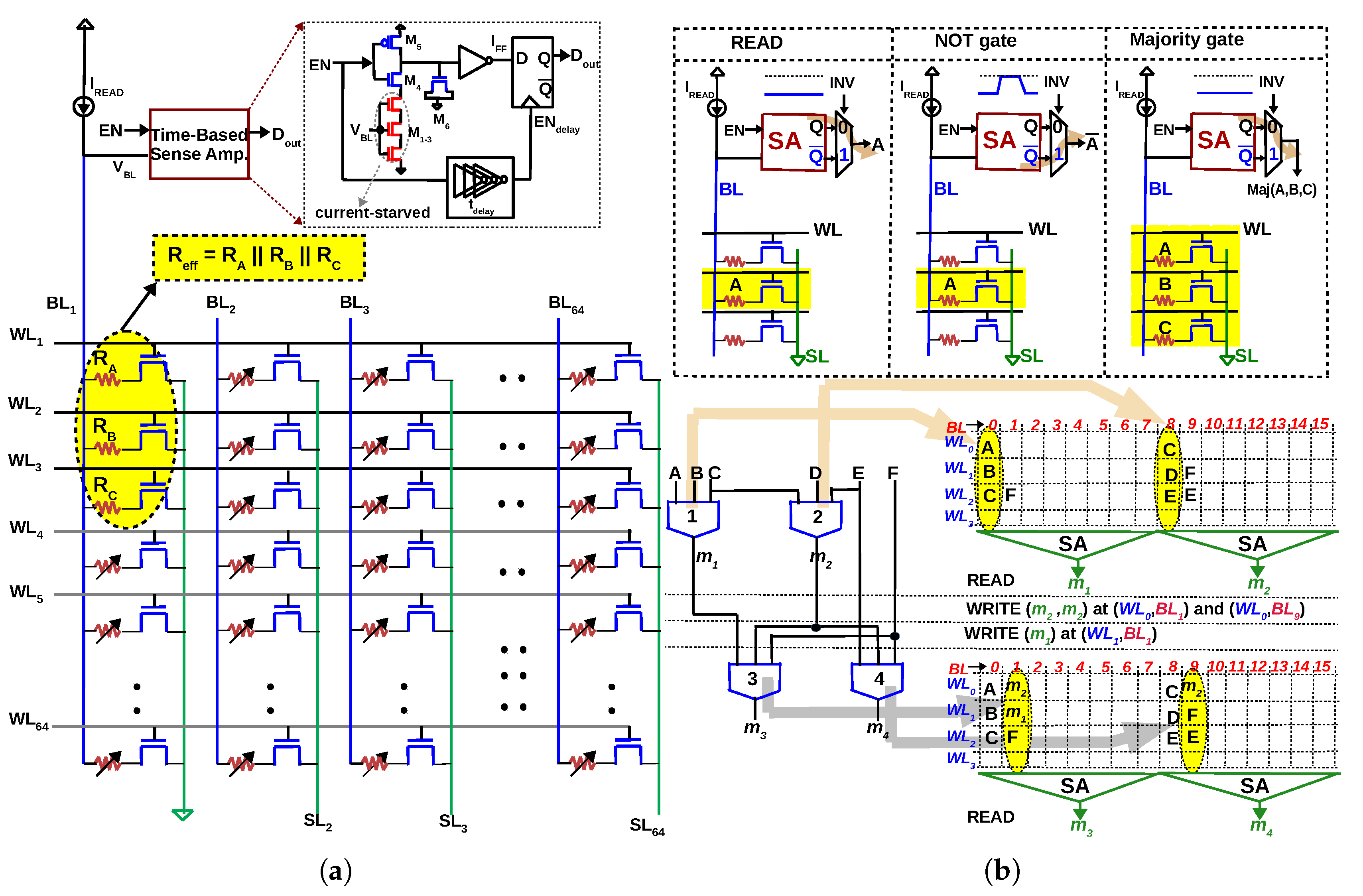
In [45,46], a majority gate is implemented while reading from a 1T–1R array, i.e., the inputs of the majority gate are the resistances of the cells and the output is sensed as a voltage, a R–V logic. Consider an array of RRAM cells arranged in a 1T-1R configuration, as depicted in Figure 3. Each cell can be individually read/written into by activating the corresponding wordline () and applying appropriate voltage across the cell ( and ). Now, if three rows are activated simultaneously during read operation (Rows 1 to 3 in Figure 3a, the resistances in column 1 are in parallel (neglecting the parasitic resistance of and ). The effective resistance between and will therefore be = (), if the drain-to-source resistance of transistor () is small compared to LRS. A Sense Amplifier (SA) which can accurately sense the effective resistance implements a ‘in-memory’ majority gate. Table 2 lists the truth table of a 3-input majority gate () and the effective resistance for all the eight possibilities. If we assume a LRS and HRS of 10 k and 133 k, respectively (IHP’s RRAM), the crucial aspect of the proposed gate is to be able to differentiate between (two LRS and one HRS) and (two HRS and one LRS). In other words, resistance ≤ 4.8 k must be sensed as ‘0’ and resistance ≥ 8.7 k must be sensed as ‘1’ (shaded grey in Table 2). If we call the resistance to be differentiated as sensing window (8.7 k− 4.8 k = 3.9 k), any sense amplifier which can differentiate this sensing window can be used to implement the majority gate. A current-mode SA is used in [45] and a time-based SA is used in [46] to verify the correct functioning of majority gate, even in the presence of reasonable RRAM variations. It must be noted unlike NAND and NOR, majority as a logic primitive is not functionally complete. However, it forms a functionally complete logic when used together with NOT, i.e., any Boolean logic can be expressed in terms of majority and NOT gates [12]. Therefore, a NOT gate is implemented by latching the inverted output of the SA, as illustrated in Figure 3b.
A comparison between V–R logic and R–V logic is presented pictorially in Figure 4. In the V–R implementation [42,43,44] in memory, the inputs of the majority gate are applied as voltages at . This manner of computation complicates the row/column decoders of the memory array, which were conventionally used to select rows/columns. Thus the peripheral circuitry will get complicated, i.e., the row/column decoders have to be significantly modified to do row selection (during memory operation) and apply inputs (during majority operation). In contrast, in the R–V implementation [45,46], the row/column decoders retain their functionality as in a conventional memory, with a minor modification (the row decoder must be enhanced to select three rows during majority operation, which can be achieved by interleaving decoders [46]). Furthermore, the R–V implementation [45,46] is conducive for parallel-processing since multiple gates can be mapped to the same set of rows, as illustrated in in Figure 4. This will aid the implementation of in-memory parallel-prefix adders (Section 5) and ternary computing [47].
4. In-Memory One-Bit Full Adders Using Different Logic Primitives
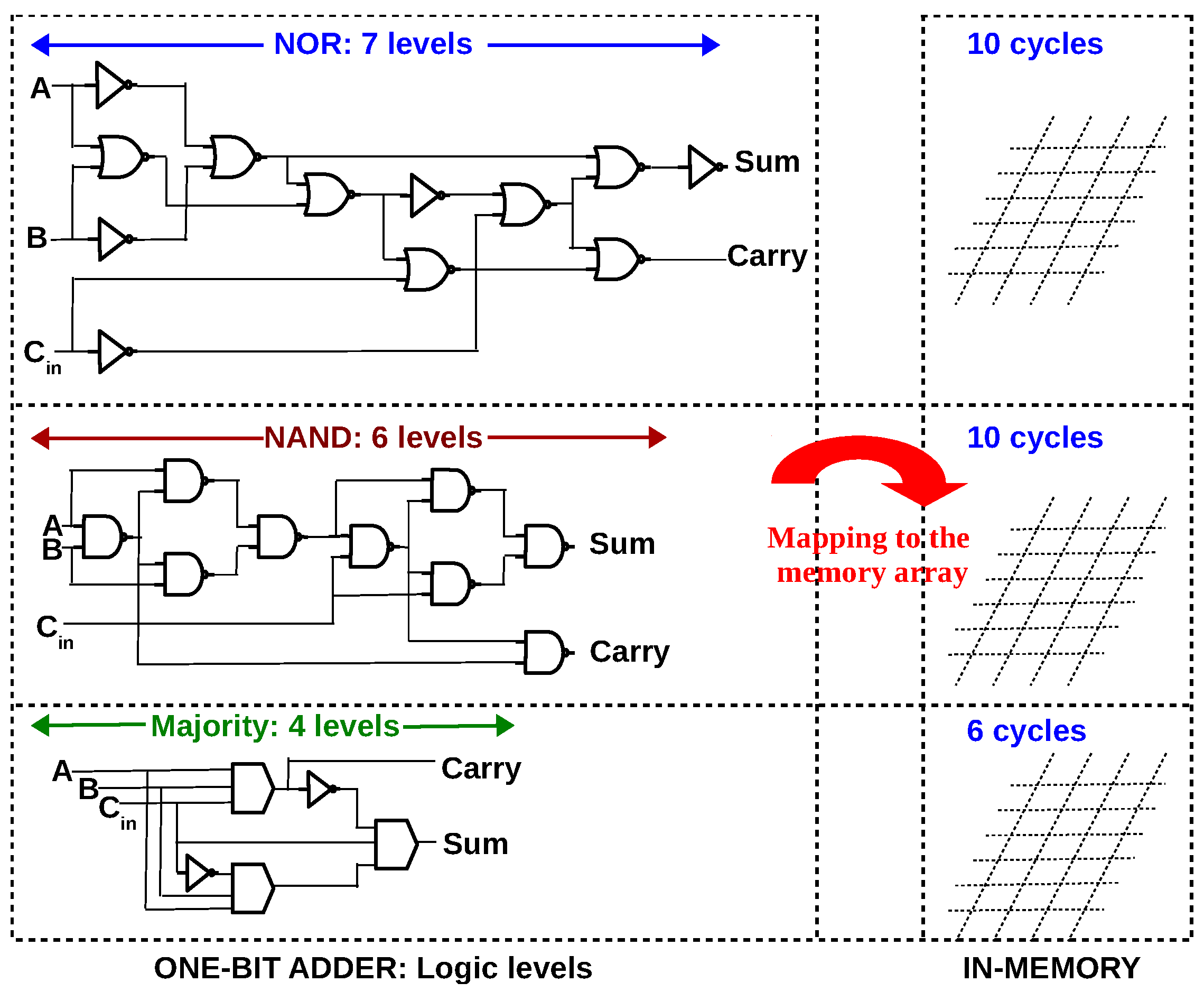
As stated, in-memory addition is achieved by a sequence of Boolean logic operations executed in memory. To compute in memory, the circuit must first be expressed in terms of the logic gates the particular memristive logic family implements. A one-bit full adder in memristive logic family based on NOR [48], NAND [49] and MAJORITY [45] is compared in Figure 5. It is evident that the number of steps (memory cycles) to compute in memory is larger than the number of logic levels. When mapped to the memory array, n levels of logic will require cycles, where x depends on the characteristics of the memristive logic family. This includes attributes like statefulness, capability to executes gates in parallel etc. In a non-stateful logic family, the output of the gate may be a voltage and it may be needed as resistance for the next level of logic, requiring an additional WRITE operation. In a stateful logic family, the output of the gate needs to be aligned with the inputs of following gate (next logic level), requiring an additional WRITE operation. In this manner, the interconnecting wires between logic levels contribute to additional cycles in memory. Furthermore, a memristive logic family should have the capability to execute multiple gates simultaneously. Consequently, multiple gates in a logic level can be mapped to the memory array in a single cycle. If the memristive logic family does not support the simultaneous execution of multiple gates, x will increase. Thus the parallel-friendliness of the logic family is also an important characteristic to minimize latency.
To evaluate the effectiveness of majority logic for in-memory computing, one-bit adders using different logic primitives are analysed from literature. Table 3 lists the latency of one-bit adders. IMPLY logic primitive was the most researched logic primitive because of it’s stateful nature. IMPLY was explored in different array configurations (1S–1R, 1T–1R) and the full adder, expressed in terms of XOR and AND gates was implemented as sequence of IMPLY operations. However, all the adders using IMPLY primitive have a latency of at least 13 cycles, implying a weak primitive. As summarized in Table 3, the number of steps to compute in an array, reduces from IMPLY to NAND/NOR logic primitive, and, further from NAND/NOR to MAJORITY, proving the strength of majority as a logic primitive.
5. In-Memory Eight-Bit Adders Using Different Logic Primitives
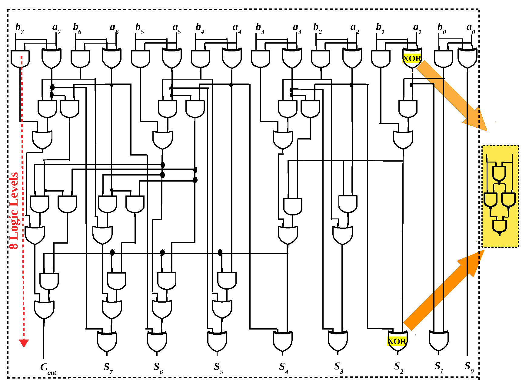
Will the reduced latency obtained by majority logic for 1-bit full adder translate to n-bit adders? In this section, eight-bit adders using different logic primitives are analysed and compared to answer this question. From Figure 5, it is evident that to minimize in-memory latency, the number of logic levels which is mapped to the memory array must be minimized. Parallel-prefix (PP) adders are a family of adders originally proposed to overcome the latency incurred by the rippling of carry in ripple carry adders. Such adders have the capability to minimize the latency to O(log n), for n-bit adders. PP adders are conventionally expressed as “propagate” () and “generate” terms (). Hence, they are implemented as AND, OR and XOR gates. As already stated, a memristive logic family cannot implement such a heterogeneity of gates. As illustrated in Figure 6, the XOR gate has to be implemented as NAND gates [37,49], increasing the logic levels to 12. Such an eight-bit PP adder (Sklansky) is expressed in OR/AND logic primitive and implemented in the memory array in 37 cycles [57]. Using majority logic, an 8-bit PP adder is implemented in memory in [46]. Since majority gate is the basic building block for many emerging nanotechnologies, prior works [13,14] have formulated such PP adders in majority logic. The majority-based eight-bit adder depicted in Figure 7 is derived from [13,14]. For an eight-bit adder, the logical depth is six levels of majority gates and one level of NOT gates, and at most eight gates are needed simultaneously in each level. Since multiple majority gates can be executed in parallel (Figure 4), they can be mapped to the array in 19 cycles, as elaborated in [46].
A detailed comparison of the latency of 8-bit in-memory adders based on different logic primitives and the corresponding adder configuration is presented in Table 4. Since IMPLY logic incurred highest latency for 1-bit addition, the trend continues for 8-bit addition which is to be expected. In ripple carry configuration, IMPLY logic based adders incur a latency of at least 54 steps and parallel-prefix configuration could reduce it to 25 steps. It may be safe to conclude that for the same logic primitive, parallel-prefix configurations results in lower latency, although the mapping of the parallel-prefix adder to the memory array is not clearly elaborated in [58]. Regarding NOR, a carry look-ahead configuration incurs 48 steps while a computerised algorithm is used to map 8-bit NOR-based adder to the memory array in 38 steps. OR/AND-based logic primitive could achieve a latency of 37 steps in parallel-prefix configuration. An eight-bit parallel-prefix adder in majority logic could achieve a latency of 19 steps [46]. Finally, a XOR-based adder [59] could achieve a latency of 16 steps even in ripple carry configuration, but it must be emphasized that [59] used multiple arrays since multiple XOR gates could not be executed simultaneously in the same array. To conclude, the latency minimization achieved by majority logic for 1-bit addition does extend to 8-bit addition. Majority logic used in synergy with parallel-prefix configuration is one of the best performing in-memory adders. Finally, any comparison among in-memory adders is not complete without considering energy consumption and area of the memory array and the peripheral circuitry needed to implement the logic operations in memory. Such a holistic comparison is beyond the scope of this work. However, latency can be a good measure of performance if the individual logic operations are achieved in an energy efficient manner and sneak-path energy leakage is avoided (in 1S–1R configuration). Note that there are other works implementing adders using memristors along with CMOS in a non-array configuration. However, such works are not included in the comparisons performed in this work since they cannot be exploited for in-memory computing.
Latency is a big hurdle for mainstream adoption of in-memory arithmetic. As noted in Table 3 and Table 4, in-memory adders require tens of steps for addition operations. Even if a single step takes 5 (RRAMs can switch in a few ), this would be much larger than the latency incurred in CMOS technology (32-bit addition operation can be performed in 4 in CMOS technology [62]). However, in in-memory arithmetic, the energy and latency (hundreds of ) for data movement is avoided (the numbers to be added have to be moved from DRAM memory to processor in conventional approach). Therefore, in-memory arithmetic can still be beneficial, provided the latency to compute in memory is minimized. The power of majority logic lies in reducing this latency to compute in memory array.
6. Conclusions
Majority logic did not become the dominant logic to compute in CMOS technology because it was more efficient to implement NAND/NOR gate than a majority gate (12 transistors for an inverted majority gate compared to 6 transistors for NAND3/NOR3). However, in many emerging post-CMOS devices, a majority gate can be implemented efficiently and therefore, majority logic needs to be re-evaluated for its computing efficiency. This review attempted to investigate the efficiency of majority logic from the perspective of in-memory computing. When the logic levels are minimized and mapped to the memory array using a memristive logic family (which can implement an in-memory majority gate), it leads to a latency optimized in-memory adder. Unlike CMOS implementation which accommodated a heterogeneity of logic gates, in-memory computing favours a homogeneous implementation of logic gates because peripheral circuitry of the array needs to be enhanced with capability to execute a particular logic primitive (different logic primitives necessitate different modifications to the peripheral circuitry). Therefore, majority-based memristive logic may be all the more preferred since they can implement any logic succinctly when used together with NOT gates. Comparisons with different logic primitives revealed that majority logic incurs least latency for 1-bit adders. For n-bit adders, majority logic has the potential to achieve a latency reduction of 70% and 50% when compared to IMPLY and NAND/NOR logic primitives, if implemented in a parallel-prefix configuration in the memory array. Minimizing latency also aids in lowering the power consumption since the array will be powered for a shorter time. Latency is a significant disadvantage in in-memory addition and the power of majority logic lies in reducing this latency. Therefore, majority logic and its advantages needs to be rediscovered in the era of in-memory computing.
Funding
This research received no external funding.
Conflicts of Interest
The author declares no conflict of interest.
References
- Theis, T.N.; Wong, H.P. The End of Moore’s Law: A New Beginning for Information Technology. Comput. Sci. Eng. 2017, 19, 41–50. [Google Scholar] [CrossRef]
- Bohr, M.T.; Young, I.A. CMOS Scaling Trends and Beyond. IEEE Micro 2017, 37, 20–29. [Google Scholar] [CrossRef]
- Shalf, J.M.; Leland, R. Computing beyond Moore’s Law. Computer 2015, 48, 14–23. [Google Scholar] [CrossRef]
- Nikonov, D.E.; Young, I.A. Benchmarking of Beyond-CMOS Exploratory Devices for Logic Integrated Circuits. IEEE J. Explor. Solid State Comput. Devices Circuits 2015, 1, 3–11. [Google Scholar] [CrossRef]
- Testa, E.; Soeken, M.; Amar, L.G.; De Micheli, G. Logic Synthesis for Established and Emerging Computing. Proc. IEEE 2019, 107, 165–184. [Google Scholar] [CrossRef]
- Young, I.A.; Nikonov, D.E. Principles and trends in quantum nano-electronics and nano-magnetics for beyond-CMOS computing. In Proceedings of the 2017 47th European Solid-State Device Research Conference (ESSDERC), Leuven, Belgium, 11–14 September 2017; pp. 1–5. [Google Scholar]
- Ciubotaru, F.; Talmelli, G.; Devolder, T.; Zografos, O.; Heyns, M.; Adelmann, C.; Radu, I.P. First experimental demonstration of a scalable linear majority gate based on spin waves. In Proceedings of the 2018 IEEE International Electron Devices Meeting (IEDM), San Francisco, CA, USA, 1–5 December 2018; pp. 36.1.1–36.1.4. [Google Scholar] [CrossRef]
- Imre, A.; Csaba, G.; Ji, L.; Orlov, A.; Bernstein, G.H.; Porod, W. Majority Logic Gate for Magnetic Quantum-Dot Cellular Automata. Science 2006, 311, 205–208. [Google Scholar] [CrossRef] [PubMed]
- Breitkreutz, S.; Kiermaier, J.; Eichwald, I.; Ju, X.; Csaba, G.; Schmitt-Landsiedel, D.; Becherer, M. Majority Gate for Nanomagnetic Logic With Perpendicular Magnetic Anisotropy. IEEE Trans. Magn. 2012, 48, 4336–4339. [Google Scholar] [CrossRef]
- Oya, T.; Asai, T.; Fukui, T.; Amemiya, Y. A Majority-Logic Nanodevice Using a Balanced Pair of Single-Electron Boxes. J. Nanosci. Nanotechnol. 2002, 2, 333–342. [Google Scholar] [CrossRef]
- Amarú, L.; Gaillardon, P.; De Micheli, G. Majority-based synthesis for nanotechnologies. In Proceedings of the 2016 21st Asia and South Pacific Design Automation Conference (ASP-DAC), Macau, China, 25–28 January 2016; pp. 499–502. [Google Scholar] [CrossRef] [Green Version]
- Amarú, L.; Gaillardon, P.E.; Micheli, G.D. Majority-Inverter Graph: A New Paradigm for Logic Optimization. IEEE Trans. Comput. Aided Des. Integr. Circuits Syst. 2016, 35, 806–819. [Google Scholar] [CrossRef] [Green Version]
- Jaberipur, G.; Parhami, B.; Abedi, D. Adapting Computer Arithmetic Structures to Sustainable Supercomputing in Low-Power, Majority-Logic Nanotechnologies. IEEE Trans. Sustain. Comput. 2018, 3, 262–273. [Google Scholar] [CrossRef]
- Pudi, V.; Sridharan, K.; Lombardi, F. Majority Logic Formulations for Parallel Adder Designs at Reduced Delay and Circuit Complexity. IEEE Trans. Comput. 2017, 66, 1824–1830. [Google Scholar] [CrossRef]
- Amarú, L.; Gaillardon, P.; Mitra, S.; De Micheli, G. New Logic Synthesis as Nanotechnology Enabler. Proc. IEEE 2015, 103, 2168–2195. [Google Scholar] [CrossRef]
- Parhami, B.; Abedi, D.; Jaberipur, G. Majority-Logic, its applications, and atomic-scale embodiments. Comput. Electr. Eng. 2020, 83, 106562. [Google Scholar] [CrossRef]
- Reuben, J.; Ben-Hur, R.; Wald, N.; Talati, N.; Ali, A.; Gaillardon, P.E.; Kvatinsky, S. Memristive Logic: A Framework for Evaluation and Comparison. In Proceedings of the Power And Timing Modeling, Optimization and Simulation (PATMOS), Thessaloniki, Greece, 25–27 September 2017; pp. 1–8. [Google Scholar]
- Reuben, J.; Talati, N.; Wald, N.; Ben-Hur, R.; Ali, A.H.; Gaillardon, P.E.; Kvatinsky, S. A Taxonomy and Evaluation Framework for Memristive Logic. In Handbook of Memristor Networks; Chua, L., Sirakoulis, G.C., Adamatzky, A., Eds.; Springer International Publishing: Cham, Switzerland, 2019; pp. 1065–1099. [Google Scholar] [CrossRef]
- Simmons, J.G.; Verderber, R.R. New conduction and reversible memory phenomena in thin insulating films. Proc. R. Soc. Lond. Ser. A Math. Phys. Sci. 1967, 301, 77–102. [Google Scholar] [CrossRef]
- Borghetti, J.; Snider, G.S.; Kuekes, P.J.; Yang, J.J.; Stewart, D.R.; Williams, R.S. ‘Memristive’ switches enable ‘stateful’ logic operations via material implication. Nature 2010, 464, 873–876. [Google Scholar] [CrossRef]
- Zhou, F.; Guckert, L.; Chang, Y.F.; Swartzlander, E.E.; Lee, J. Bidirectional voltage biased implication operations using SiOx based unipolar memristors. Appl. Phys. Lett. 2015, 107, 183501. [Google Scholar] [CrossRef]
- Talati, N.; Ben-Hur, R.; Wald, N.; Haj-Ali, A.; Reuben, J.; Kvatinsky, S. mMPU—A Real Processing-in-Memory Architecture to Combat the von Neumann Bottleneck. In Applications of Emerging Memory Technology: Beyond Storage; Suri, M., Ed.; Springer: Singapore, 2020; pp. 191–213. [Google Scholar] [CrossRef]
- Rahimi Azghadi, M.; Chen, Y.C.; Eshraghian, J.K.; Chen, J.; Lin, C.Y.; Amirsoleimani, A.; Mehonic, A.; Kenyon, A.J.; Fowler, B.; Lee, J.C.; et al. Complementary Metal-Oxide Semiconductor and Memristive Hardware for Neuromorphic Computing. Adv. Intell. Syst. 2020, 2, 1900189. [Google Scholar] [CrossRef] [Green Version]
- Chang, K.C.; Chang, T.C.; Tsai, T.M.; Zhang, R.; Hung, Y.C.; Syu, Y.E.; Chang, Y.F.; Chen, M.C.; Chu, T.J.; Chen, H.L.; et al. Physical and chemical mechanisms in oxide-based resistance random access memory. Nanoscale Res. Lett. 2015, 10. [Google Scholar] [CrossRef] [Green Version]
- Reuben, J.; Fey, D.; Wenger, C. A Modeling Methodology for Resistive RAM Based on Stanford-PKU Model With Extended Multilevel Capability. IEEE Trans. Nanotechnol. 2019, 18, 647–656. [Google Scholar] [CrossRef] [Green Version]
- Golonzka, O.; Arslan, U.; Bai, P.; Bohr, M.; Baykan, O.; Chang, Y.; Chaudhari, A.; Chen, A.; Clarke, J.; Connor, C.; et al. Non-Volatile RRAM Embedded into 22FFL FinFET Technology. In Proceedings of the 2019 Symposium on VLSI Technology, Kyoto, Japan, 9–14 June 2019; pp. T230–T231. [Google Scholar] [CrossRef]
- Hsieh, C.C.; Chang, Y.F.; Chen, Y.C.; Shahrjerdi, D.; Banerjee, S.K. Highly Non-linear and Reliable Amorphous Silicon Based Back-to-Back Schottky Diode as Selector Device for Large Scale RRAM Arrays. ECS J. Solid State Sci. Technol. 2017, 6, N143–N147. [Google Scholar] [CrossRef] [Green Version]
- Lin, C.Y.; Chen, P.H.; Chang, T.C.; Chang, K.C.; Zhang, S.D.; Tsai, T.M.; Pan, C.H.; Chen, M.C.; Su, Y.T.; Tseng, Y.T.; et al. Attaining resistive switching characteristics and selector properties by varying forming polarities in a single HfO2-based RRAM device with a vanadium electrode. Nanoscale 2017, 9, 8586–8590. [Google Scholar] [CrossRef] [PubMed]
- Kim, S.; Lin, C.Y.; Kim, M.H.; Kim, T.H.; Kim, H.; Chen, Y.C.; Chang, Y.F.; Park, B.G. Dual Functions of V/SiOx/AlOy/p++Si Device as Selector and Memory. Nanoscale Res. Lett. 2018, 13. [Google Scholar] [CrossRef]
- Chen, C.; Lin, C.; Chen, P.; Chang, T.; Shih, C.; Tseng, Y.; Zheng, H.; Chen, Y.; Chang, Y.; Lin, C.; et al. The Demonstration of Increased Selectivity During Experimental Measurement in Filament-Type Vanadium Oxide-Based Selector. IEEE Trans. Electr. Devices 2018, 65, 4622–4627. [Google Scholar] [CrossRef]
- Ben-Hur, R.; Ronen, R.; Haj-Ali, A.; Bhattacharjee, D.; Eliahu, A.; Peled, N.; Kvatinsky, S. SIMPLER MAGIC: Synthesis and Mapping of In-Memory Logic Executed in a Single Row to Improve Throughput. IEEE Trans. Comput. Aided Des. Integr. Circuits Syst. 2019. [Google Scholar] [CrossRef]
- Adam, G.C.; Hoskins, B.D.; Prezioso, M.; Strukov, D.B. Optimized stateful material implication logic for three- dimensional data manipulation. Nano Res. 2016, 9, 3914–3923. [Google Scholar] [CrossRef]
- Kumar, A.P.; Aditya, B.; Sony, G.; Prasanna, C.; Satish, A. Estimation of power and delay in CMOS circuits using LCT. Indones. J. Electr. Eng. Comput. Sci. 2019, 14, 990–998. [Google Scholar]
- Rumi, Z.; Walus, K.; Wei, W.; Jullien, G.A. A method of majority logic reduction for quantum cellular automata. IEEE Trans. Nanotechnol. 2004, 3, 443–450. [Google Scholar] [CrossRef]
- Kvatinsky, S.; Satat, G.; Wald, N.; Friedman, E.G.; Kolodny, A.; Weiser, U.C. Memristor-Based Material Implication (IMPLY) Logic: Design Principles and Methodologies. IEEE Trans. Very Larg. Scale Integr. (VLSI) Syst. 2014, 22, 2054–2066. [Google Scholar] [CrossRef]
- Lehtonen, E.; Poikonen, J.H.; Laiho, M. Memristive Stateful Logic. In Handbook of Memristor Networks; Chua, L., Sirakoulis, G.C., Adamatzky, A., Eds.; Springer International Publishing: Cham, Switzerland, 2019; pp. 1101–1121. [Google Scholar] [CrossRef]
- Shen, W.; Huang, P.; Fan, M.; Han, R.; Zhou, Z.; Gao, B.; Wu, H.; Qian, H.; Liu, L.; Liu, X.; et al. Stateful Logic Operations in One-Transistor-One- Resistor Resistive Random Access Memory Array. IEEE Electr. Device Lett. 2019, 40, 1538–1541. [Google Scholar] [CrossRef]
- Ielmini, D.; Wong, H.S.P. In-memory computing with resistive switching devices. Nat. Electr. 2018, 1, 333–343. [Google Scholar] [CrossRef]
- Gupta, S.; Imani, M.; Rosing, T. FELIX: Fast and Energy-efficient Logic in Memory. In Proceedings of the International Conference on Computer-Aided Design (ICCAD ’18), San Diego, CA, USA, 5–8 November 2018; pp. 55:1–55:7. [Google Scholar] [CrossRef]
- Reuben, J.; Fey, D. A Time-based Sensing Scheme for Multi-level Cell (MLC) Resistive RAM. In Proceedings of the 2019 IEEE Nordic Circuits and Systems Conference (NORCAS): NORCHIP and International Symposium of System-on-Chip (SoC), Helsinki, Finland, 29–30 October 2019; pp. 1–6. [Google Scholar] [CrossRef] [Green Version]
- Reuben, J.; Biglari, M.; Fey, D. Incorporating Variability of Resistive RAM in Circuit Simulations Using the Stanford–PKU Model. IEEE Trans. Nanotechnol. 2020, 19, 508–518. [Google Scholar] [CrossRef]
- Gaillardon, P.; Amaru, L.; Siemon, A.; Linn, E.; Waser, R.; Chattopadhyay, A.; De Micheli, G. The Programmable Logic-in-Memory (PLiM) computer. In Proceedings of the 2016 Design, Automation Test in Europe Conference Exhibition (DATE), Dresden, Germany, 14–18 March 2016; pp. 427–432. [Google Scholar]
- Shirinzadeh, S.; Soeken, M.; Gaillardon, P.; Drechsler, R. Logic Synthesis for RRAM-Based In-Memory Computing. IEEE Trans. Comput. Aided Des. Integr. Circuits Syst. 2018, 37, 1422–1435. [Google Scholar] [CrossRef]
- Bhattacharjee, D.; Easwaran, A.; Chattopadhyay, A. Area-constrained technology mapping for in-memory computing using ReRAM devices. In Proceedings of the 2017 22nd Asia and South Pacific Design Automation Conference (ASP-DAC), Chiba, Japan, 16–19 January 2017; pp. 69–74. [Google Scholar] [CrossRef]
- Reuben, J. Binary Addition in Resistance Switching Memory Array by Sensing Majority. Micromachines 2020, 11, 496. [Google Scholar] [CrossRef]
- Reuben, J.; Pechmann, S. A Parallel-friendly Majority Gate to Accelerate In-memory Computation. In Proceedings of the 2020 IEEE 31st International Conference on Application-Specific Systems, Architectures and Processors (ASAP), Manchester, UK, 6–8 July 2020; pp. 93–100. [Google Scholar]
- Fey, D.; Reuben, J. Direct state transfer in MLC based memristive ReRAM devices for ternary computing. In Proceedings of the 2020 European Conference on Circuit Theory and Design (ECCTD), Sofia, Bulgaria, 7–10 September 2020; pp. 1–5. [Google Scholar]
- Hur, R.B.; Wald, N.; Talati, N.; Kvatinsky, S. SIMPLE MAGIC: Synthesis and In-memory Mapping of Logic Execution for Memristor-aided Logic. In Proceedings of the 36th International Conference on Computer-Aided Design (ICCAD ’17), Irvine, CA, USA, 13–16 November 2017; pp. 225–232. [Google Scholar]
- Huang, P.; Kang, J.; Zhao, Y.; Chen, S.; Han, R.; Zhou, Z.; Chen, Z.; Ma, W.; Li, M.; Liu, L.; et al. Reconfigurable Nonvolatile Logic Operations in Resistance Switching Crossbar Array for Large-Scale Circuits. Adv. Mater. 2016, 28, 9758–9764. [Google Scholar] [CrossRef] [PubMed]
- Chang, Y.; Zhou, F.; Fowler, B.W.; Chen, Y.; Hsieh, C.; Guckert, L.; Swartzlander, E.E.; Lee, J.C. Memcomputing (Memristor + Computing) in Intrinsic SiOx-Based Resistive Switching Memory: Arithmetic Operations for Logic Applications. IEEE Trans. Electr. Devices 2017, 64, 2977–2983. [Google Scholar] [CrossRef]
- Cheng, L.; Zhang, M.Y.; Li, Y.; Zhou, Y.X.; Wang, Z.R.; Hu, S.Y.; Long, S.B.; Liu, M.; Miao, X.S. Reprogrammable logic in memristive crossbar for in-memory computing. J. Phys. D Appl. Phys. 2017, 50, 505102. [Google Scholar] [CrossRef]
- Teimoory, M.; Amirsoleimani, A.; Shamsi, J.; Ahmadi, A.; Alirezaee, S.; Ahmadi, M. Optimized implementation of memristor-based full adder by material implication logic. In Proceedings of the 2014 21st IEEE International Conference on Electronics, Circuits and Systems (ICECS), Marseille, France, 7–10 December 2014; pp. 562–565. [Google Scholar]
- Rohani, S.G.; Taherinejad, N.; Radakovits, D. A Semiparallel Full-Adder in IMPLY Logic. IEEE Trans. Very Larg. Scale Integr. (VLSI) Syst. 2019, 28, 297–301. [Google Scholar] [CrossRef]
- Kim, K.M.; Williams, R.S. A Family of Stateful Memristor Gates for Complete Cascading Logic. IEEE Trans. Circuits Syst. I Regul. Pap. 2019, 66, 4348–4355. [Google Scholar] [CrossRef]
- Siemon, A.; Drabinski, R.; Schultis, M.J.; Hu, X.; Linn, E.; Heittmann, A.; Waser, R.; Querlioz, D.; Menzel, S.; Friedman, J.S. Stateful Three-Input Logic with Memristive Switches. Sci. Rep. 2019, 9, 14618. [Google Scholar] [CrossRef] [Green Version]
- Xu, L.; Yuan, R.; Zhu, Z.; Liu, K.; Jing, Z.; Cai, Y.; Wang, Y.; Yang, Y.; Huang, R. Memristor-Based Efficient In-Memory Logic for Cryptologic and Arithmetic Applications. Adv. Mater. Technol. 2019, 4, 1900212. [Google Scholar] [CrossRef]
- Siemon, A.; Menzel, S.; Bhattacharjee, D.; Waser, R.; Chattopadhyay, A.; Linn, E. Sklansky tree adder realization in 1S1R resistive switching memory architecture. Eur. Phys. J. Spec. Top. 2019, 228, 2269–2285. [Google Scholar] [CrossRef]
- Revanna, N.; Swartzlander, E.E. Memristor based adder circuit design. In Proceedings of the 2016 50th Asilomar Conference on Signals, Systems and Computers, Pacific Grove, CA, USA, 6–9 November 2016; pp. 162–166. [Google Scholar]
- Wang, Z.; Li, Y.; Su, Y.; Zhou, Y.; Cheng, L.; Chang, T.; Xue, K.; Sze, S.M.; Miao, X. Efficient Implementation of Boolean and Full-Adder Functions with 1T1R RRAMs for Beyond Von Neumann In-Memory Computing. IEEE Trans. Electr. Devices 2018, 65, 4659–4666. [Google Scholar] [CrossRef]
- Cheng, L.; Li, Y.; Yin, K.S.; Hu, S.Y.; Su, Y.T.; Jin, M.M.; Wang, Z.R.; Chang, T.C.; Miao, X.S. Functional Demonstration of a Memristive Arithmetic Logic Unit (MemALU) for In-Memory Computing. Adv. Funct. Mater. 2019, 29, 1905660. [Google Scholar] [CrossRef]
- Kim, Y.S.; Son, M.W.; Song, H.; Park, J.; An, J.; Jeon, J.B.; Kim, G.Y.; Son, S.; Kim, K.M. Stateful In-Memory Logic System and Its Practical Implementation in a TaOx-Based Bipolar-Type Memristive Crossbar Array. Adv. Intell. Syst. 2020, 2, 1900156. [Google Scholar] [CrossRef] [Green Version]
- Xiao, T.P.; Bennett, C.H.; Hu, X.; Feinberg, B.; Jacobs-Gedrim, R.; Agarwal, S.; Brunhaver, J.S.; Friedman, J.S.; Incorvia, J.A.C.; Marinella, M.J. Energy and Performance Benchmarking of a Domain Wall-Magnetic Tunnel Junction Multibit Adder. IEEE J. Explor. Solid State Comput. Devices Circuits 2019, 5, 188–196. [Google Scholar] [CrossRef]
Figure 1.
(a) 1S–1R and 1T–1R configuration of memristive memory array (b) If resistance is the only state variable, a memristive logic is said to be stateful. If voltage is also used in addition to resistance, it is said to be non-stateful (c) 1-bit full adder in terms of NOR gates [31], NAND gates [32,33] and majority gates [34]; Majority logic achieves less logical depth than NAND/NOR for 1-bit full adder.

Figure 2.
Illustration of V–R majority logic. Arrow indicates the state transition, which depends on the initial state of the RRAM cell C and the voltage applied across its terminals (); dotted lines indicate the state variable of C, which is resistance, while A and B are voltages [18].
Figure 2.
Illustration of V–R majority logic. Arrow indicates the state transition, which depends on the initial state of the RRAM cell C and the voltage applied across its terminals (); dotted lines indicate the state variable of C, which is resistance, while A and B are voltages [18].

Figure 3.
(a) In-memory majority gate proposed in [45,46]: When three rows are activated () simultaneously in a 1T-1R array, the three resistances will be in parallel (Inputs of the majority gate are represented as resistances ). An ‘in-memory’ majority gate can be implemented by accurately sensing the effective resistance during READ. (b) NOT operation implemented with a 2:1 multiplexer at the output of the SA. With majority and NOT gate implemented as READ, multiple levels of logic can be executed by writing the data back to the array, simplifying computing to READ and WRITE operations in memory. Multiple majority gates can be executed in parallel in the memory array, thereby reducing latency of in-memory computation.

Figure 4.
(a) V–R majority gate [42,43,44] (b) R–V majority gate [45,46] (c) When multiple gates have to be executed in parallel, the majority gates of [42,43,44] have to be mapped diagonally because two gates cannot be executed in the same row/column.

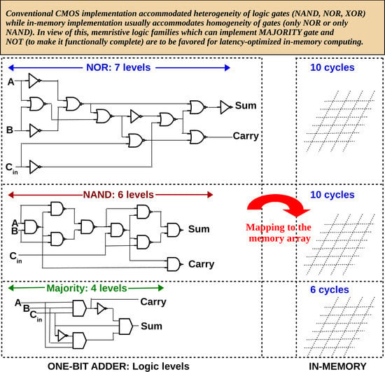
Figure 5.
n levels of Boolean logic will require cycles in-memory, where x depends on the memristive logic family. It must be noted that the number of cycles required (10 cycles for NOR, NAND and 6 cycles for MAJORITY) is already optimized by executing multiple gates in parallel (see the mapping for NOR [31], NAND [49] and MAJORITY [45]).

Figure 6.
An eight-bit parallel-prefix adder (Ladner-Fischer) has 8 logic levels of AND, OR and XOR gates. If the logic family cannot execute XOR gate, it must be expressed as NAND gates, increasing the logic levels to 12.
Figure 6.
An eight-bit parallel-prefix adder (Ladner-Fischer) has 8 logic levels of AND, OR and XOR gates. If the logic family cannot execute XOR gate, it must be expressed as NAND gates, increasing the logic levels to 12.

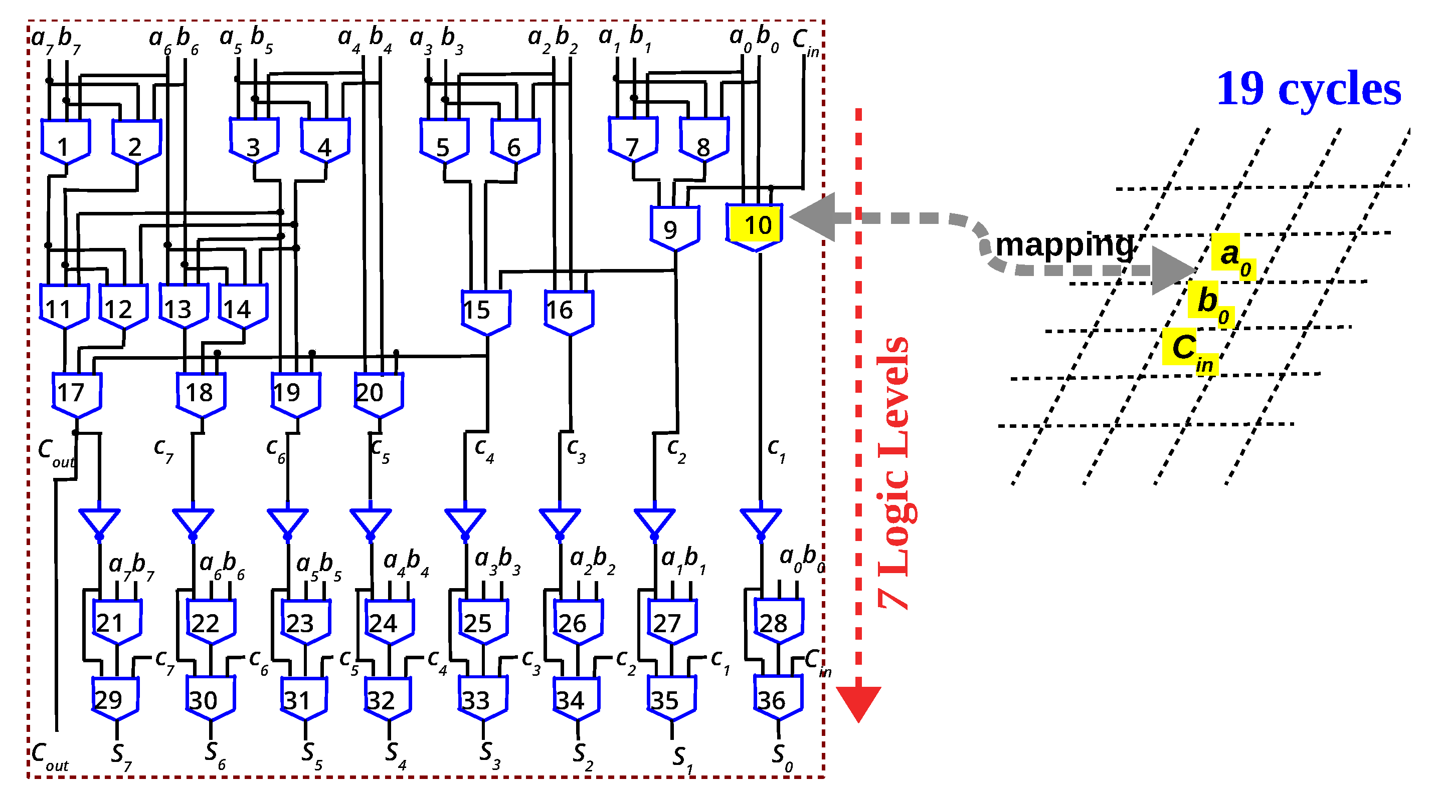
Figure 7.
Eight-bit parallel-prefix adder (Ladner-Fischer) expressed as 7 levels of Majority+NOT gates. By executing multiple gates in parallel, the adder can be implemented in memory in 19 cycles, as elaborated in [46].
Figure 7.
Eight-bit parallel-prefix adder (Ladner-Fischer) expressed as 7 levels of Majority+NOT gates. By executing multiple gates in parallel, the adder can be implemented in memory in 19 cycles, as elaborated in [46].


Table 1.
Establishing the link between the majority function and Resistive RAM.
| A | B | C | ||||
|---|---|---|---|---|---|---|
| 0 | 0 | 0 | 0 | 1 | 0 | 0 |
| 0 | 0 | 1 | 0 | 1 | 1 | 1 |
| 0 | 1 | 0 | 0 | 0 | 0 | 0 |
| 0 | 1 | 1 | 1 | 0 | 0 | 0 |
| 1 | 0 | 0 | 0 | 1 | 1 | 1 |
| 1 | 0 | 1 | 1 | 1 | 1 | 1 |
| 1 | 1 | 0 | 1 | 0 | 0 | 0 |
| 1 | 1 | 1 | 1 | 0 | 1 | 1 |
Table 2.
Precisely sensing results in majority: Logic ‘0’ is LRS (10 k) and logic ‘1’ is HRS (133.3 k). Sense amplifier distinguishes between rows shaded grey and those that are not.
Table 2.
Precisely sensing results in majority: Logic ‘0’ is LRS (10 k) and logic ‘1’ is HRS (133.3 k). Sense amplifier distinguishes between rows shaded grey and those that are not.
| A | B | C | |||
|---|---|---|---|---|---|
| 0 | 0 | 0 | 0 | 3.3 k | |
| 0 | 0 | 1 | 0 | 4.8 k | |
| 0 | 1 | 0 | 0 | 4.8 k | |
| 0 | 1 | 1 | 1 | 8.7 k | |
| 1 | 0 | 0 | 0 | 4.8 k | |
| 1 | 0 | 1 | 1 | 8.7 k | |
| 1 | 1 | 0 | 1 | 8.7 k | |
| 1 | 1 | 1 | 1 | 44.4 k |
Table 3.
Latency of in-memory one-bit full adders.
| Primitive | Structure | Latency | Ref |
|---|---|---|---|
| IMPLY | 1D–1R | 43 steps | [50] |
| IMPLY | 1R | 35 steps | [32] |
| IMPLY | 1R | 27 steps | [51] |
| IMPLY | 1R | 23 steps | [52] |
| IMPLY(semi-parallel) | 1T–1R | 17 steps | [53] |
| IMPLY | 1T–1R | 13 steps | [54] |
| ORNOR | 1T–1R | 17 steps | [55] |
| NOR | 1S–1R | 10 steps | [48] |
| NAND | 1S–1R | 10 steps | [49] |
| XOR+NAND (unipolar memristors) | 1S–1R | 8 steps | [56] |
| MAJORITY+NOT | 1T–1R | 6 steps | [45] |
Table 4.
Latency of in-memory 8-bit adders.
| Primitive | Array | Adder Type | Latency | Comment/Ref |
|---|---|---|---|---|
| IMPLY | 1S-1R | Ripple carry | 58 | Each step is IMPLY operation [35] |
| IMPLY+OR | 1S-1R | Ripple Carry | 54 | Each step is IMPLY/OR/NOR operation [60] |
| IMPLY | – | Parallel-prefix | 25 | Each step is IMPLY operation [58] |
| NOR/NOT | 1T-1R | Look-Ahead | 48 | Each step has one or more NOR/NOT operations [61] |
| NOR | 1S-1R | algorithm | 38 | Each step has one or more NOR operations [18] |
| OR/AND | 1S-1R | Parallel-prefix | 37 | Each step has one or more OR/AND operation [57] |
| ORNOR | 1S-1R | Parallel-clocking | 31 | Each step has one or more ORNOR/IMPLY operation [55] |
| MAJORITY+NOT | 1T-1R | Parallel-prefix | 19 | Each step is Majority/NOT or WRITE [46] |
| XOR | 1T-1R | Ripple carry | 16 * | Each step is XOR [59] |
* XOR gate proposed in [59] is not parallel-friendly and consequently multiple gates cannot be executed in parallel in the array (to circumvent this, multiple arrays have been used in [59]). Furthermore, XOR is not functionally complete and has to be used in conjunction with other gates to implement other arithmetic circuits. In contrast, majority+NOT is functionally complete.
© 2020 by the author. Licensee MDPI, Basel, Switzerland. This article is an open access article distributed under the terms and conditions of the Creative Commons Attribution (CC BY) license (http://creativecommons.org/licenses/by/4.0/).
Share and Cite
MDPI and ACS Style
Reuben, J. Rediscovering Majority Logic in the Post-CMOS Era: A Perspective from In-Memory Computing. J. Low Power Electron. Appl. 2020, 10, 28. https://doi.org/10.3390/jlpea10030028
AMA Style
Reuben J. Rediscovering Majority Logic in the Post-CMOS Era: A Perspective from In-Memory Computing. Journal of Low Power Electronics and Applications. 2020; 10(3):28. https://doi.org/10.3390/jlpea10030028
Chicago/Turabian StyleReuben, John. 2020. "Rediscovering Majority Logic in the Post-CMOS Era: A Perspective from In-Memory Computing" Journal of Low Power Electronics and Applications 10, no. 3: 28. https://doi.org/10.3390/jlpea10030028
Note that from the first issue of 2016, this journal uses article numbers instead of page numbers. See further details here.