Article

Electrical Conduction Properties of Hydrogenated Amorphous Carbon Films with Different Structures

1
Department of Mechanical Engineering, Tokyo Institute of Technology, 2-12-1, O-okayama, Meguro-ku, Tokyo 152-8550, Japan
2
Synchrotron Light Research Institute (Public Organization), 111 University Avenue, Nakhon Ratchasima 30000, Thailand
3
Institute of Innovative Research, Tokyo Institute of Technology, 4259 Nagatsuta, Midori-ku, Yokohama, Kanagawa 226-8503, Japan
*
Author to whom correspondence should be addressed.
Materials 2021, 14(9), 2355; https://doi.org/10.3390/ma14092355
Submission received: 18 March 2021 / Revised: 23 April 2021 / Accepted: 28 April 2021 / Published: 1 May 2021
(This article belongs to the Special Issue DLC (Diamond-Like Carbon) Film Formation and Application)

Abstract

:
Hydrogenated amorphous carbon (a-C:H) films have optical and electrical properties that vary widely depending on deposition conditions; however, the electrical conduction mechanism, which is dependent on the film structure, has not yet been fully revealed. To understand the relationship between the film structure and electrical conduction mechanism, three types of a-C:H films were prepared and their film structures and electrical properties were evaluated. The sp2/(sp2 + sp3) ratios were measured by a near-edge X-ray absorption fine structure technique. From the conductivity–temperature relationship, variable-range hopping (VRH) conduction was shown to be the dominant conduction mechanism at low temperatures, and the electrical conduction mechanism changed at a transition temperature from VRH conduction to thermally activated band conduction. On the basis of structural analyses, a model of the microstructure of a-C:H that consists of sp2 and sp3-bonded carbon clusters, hydrogen atoms and dangling bonds was built. Furthermore, it is explained how several electrical conduction parameters are affected by the carrier transportation path among the clusters.

1. Introduction

Hydrogenated amorphous carbon (a-C:H) films are a non-crystalline material [1]. They consist of sp2 and sp3-hybridized bonded carbon atoms and hydrogen atoms. The most popular process to synthesize a-C:H films is plasma-enhanced chemical vapor deposition (PECVD) [2]. The mechanical and tribological properties of a-C:H films depend on their atomic structure [3]. These films, and particularly what is called diamond-like carbon (DLC) films, have outstanding mechanical properties, such as high hardness, low coefficients of friction and excellent corrosion and wear resistance. Fiaschi et al. reported that the hardness of DLC films depends on their sp3 content and that the hardness affects tribological properties [3]. Many researchers have mentioned that the friction coefficient and specific rate of the films were affected by their hydrogen content [4,5,6]. From these studies, there have been clarifications made of the relationship between the mechanical properties of a-C:H film and the sp2/sp3 carbon–bonding ratio, and also the relationship between the mechanical properties of a-C:H films and the amount of hydrogen. As a result of this clarification, the a-C: H film with the optimum mechanical properties for use in a given environment has been applied to the surfaces of mechanical parts. [1,7,8,9]. Another notable feature of a-C:H films is that they have a wide range of physical properties resulting from their structural flexibility. The sp2/sp3 ratio and hydrogen content can be controlled in the range of 0.3–0.9 and 0.1–0.6, respectively [8,10]. These structural factors depend on the deposition condition [1]. Their electrical and electronic properties also change. The optical band gap and electrical resistivity are in the range of 0.5–4.5 eV [11,12,13], and 102–1016 Ω·cm [14], respectively. These films therefore have the potential to be used as semiconductor materials that offer widely variable optical and electrical properties.
The most commonly used amorphous semiconductor material is hydrogenated amorphous silicon (a-Si:H). The properties of a-Si:H have been studied intensively for electronic applications in industry [15,16,17]. Spear and Le Comber found that a-Si:H could be substitutionally doped by boron and phosphorus by adding diborane or phosphine to the source silane gas stream [18]. Hydrogen incorporated in a-Si:H terminates the dangling bonds, which causes structural relaxation. As a result, localized states in the band gap significantly decrease and doping is made possible.
Unlike silicon, carbon can form three types of covalent bonds because of its ability to form hybrid orbitals of sp, sp2 and sp3. In a-C:H, there exist mainly sp2 and sp3 hybridized carbon simultaneously [8,19]. For sp2 hybridized carbon, the 2s orbital is mixed with two 2p orbitals to form three equivalent sp2 orbitals and one remaining p orbital. The overlap of p orbitals on adjacent carbon atoms forms π bonds. These π bonds are accompanied by sp2 hybridization that creates electronic states near the Fermi level and thus determines the electronic properties [20,21,22,23]. The π states are strongly affected by the interatomic distance and atomic coordination. It is therefore expected that the mechanism of electrical conduction in a-C:H differs considerably from that of a-Si:H. While many a-C:H films have been applied in the mechanical field, the scientific reports of electrical and electronic properties of the films are very limited and the relationship between the basic structural factor and these properties is still not clear.
Hydrogenated amorphous carbon began to attract attention as a semiconductor material after a-Si:H had already become the most commonly used amorphous semiconductor material [13]. As with a-Si:H, a-C:H can be synthesized over large areas and grown to have graded properties by controlling deposition conditions during the film growth. Meyerson and Smith found that a-C:H could be doped by adding B2H6 or PH3 in a similar manner to a-Si:H [24]. In addition, a-C:H films can be produced from relatively safer and lower-cost source materials such as hydrocarbon and graphite. Hence, a-C:H films are expected to be applied to devices such as solar cells and thin-film transistors (TFT) [13]. Fundamental research focused on the electrical conduction mechanism in a-C:H films was conducted by Fabisiak et al. [25]. They showed that the temperature dependence of the electrical conductivity of a-C:H films indicate thermally activated band conduction at high temperatures and variable-range hopping (VRH) conduction at low temperatures [25]. The functional relationship for thermally activated band conduction in the extended state is given by the following expression [26]:
σ b = σ 0 exp ( E a k B T )
and the functional relationship for VRH conduction in the localized states near the Fermi level is given by the following expression [27]:
σ h = σ 00 exp [ ( T 0 T ) 1 / 4 ]
where Ea is the activation energy, kB the Boltzmann constant, T0 the Mott’s characteristic temperature and T the absolute temperature.
There are, however, few practical applications of a-C:H films in the field of electrical and electronic engineering because their electrical-conduction mechanism has not yet been fully revealed. There has been only a limited number of studies on a-C:H films seeking to explain the relationship between their electrical properties and film structure and, in particular, to explain the effect of sp2/sp3 ratio and hydrogen content on this relationship. This is thought to be because it is difficult to evaluate the sp2/sp3 ratio quantitatively. The effect of the presence of both sp3 and sp2 bonding on the properties of the films is still unclear. For electrical and electronic applications using a-C:H films to progress, it is important to investigate the relationship between film structure and electrical properties and it is necessary to determine which structures are better for such applications.
In this study, three types of a-C:H films were deposited from three different hydrocarbons, and then the relationship between the film structure and conduction characteristics of the films was investigated. To determine the film structure and hydrogen content, the sp2/(sp2 + sp3) ratio and sp2 cluster size in the films were evaluated. Temperature dependence of electrical conductivity is characterized by several parameters that indirectly reflect the atomic structure: activation energy (Ea), transition temperature of conduction mechanisms (Tc) and Mott’s characteristic temperature (T0). On the basis of this dependence, a model giving an explanation of how the electrical conduction mechanism will change due to the variation of the structure was proposed.

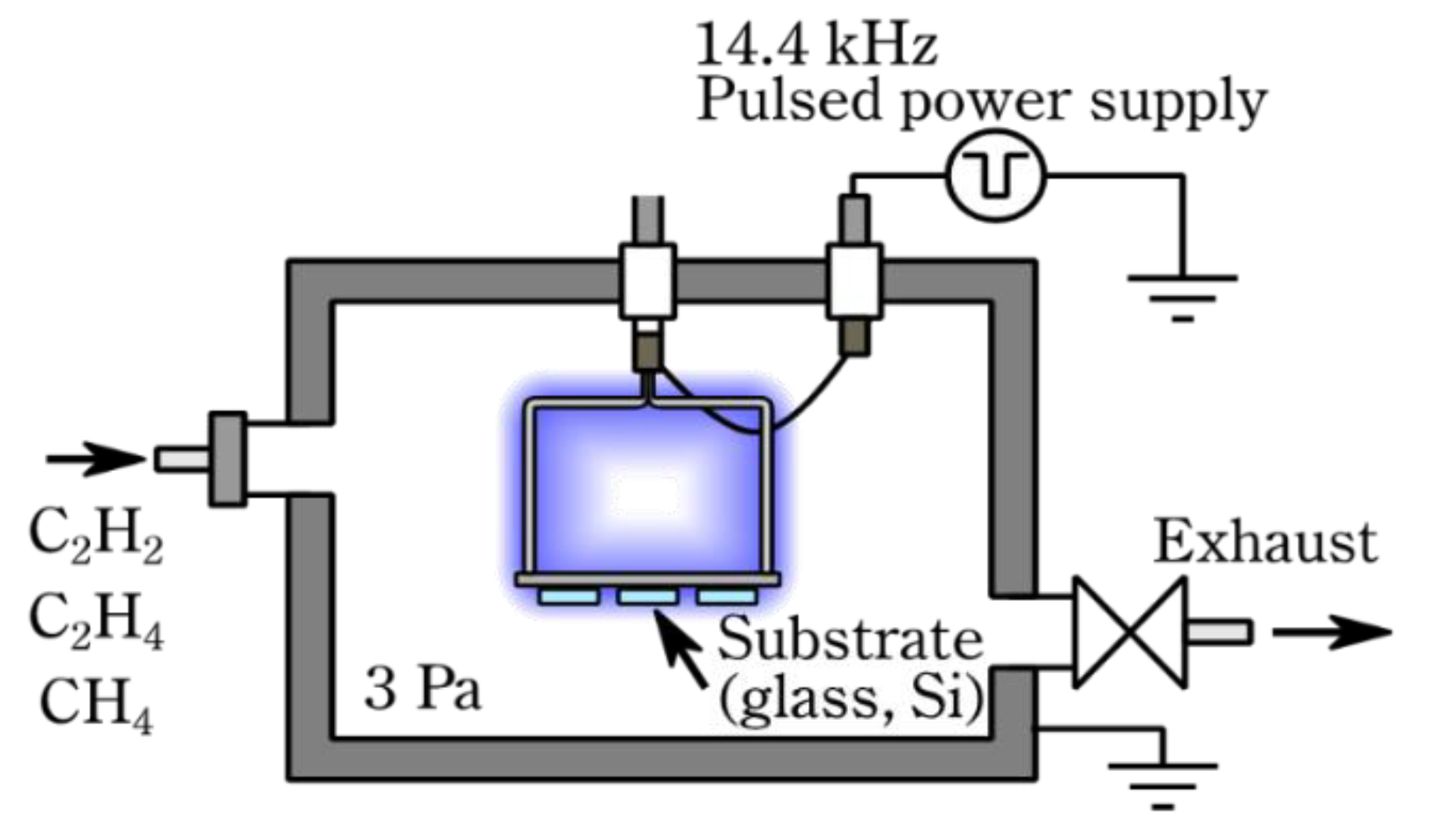
2. Materials and Methods
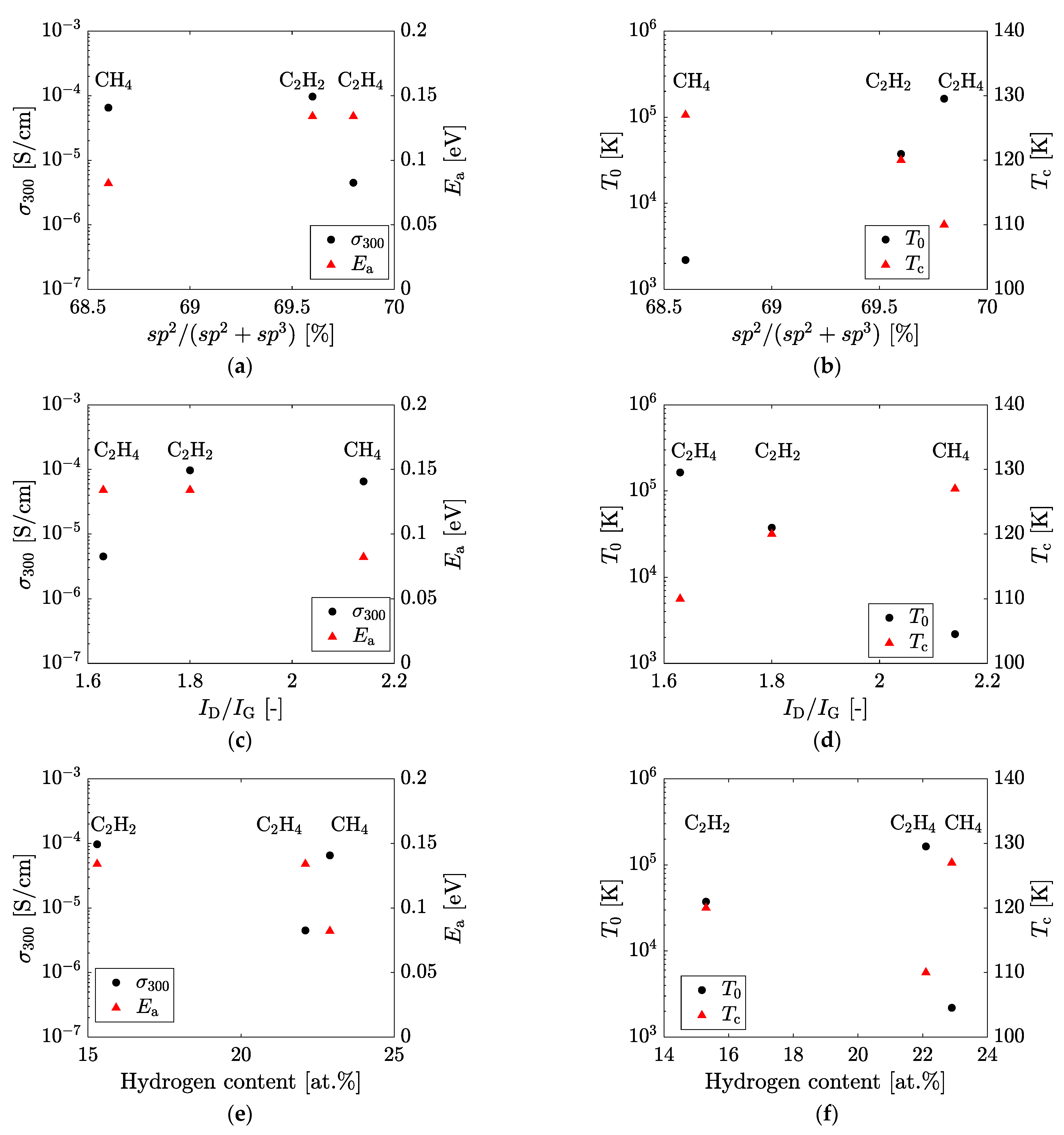
The a-C:H films were prepared by pulsed plasma-enhanced chemical vapor deposition (CVD) [28]. We deposited 3 types of a-C:H films on 100 p-Si substrates (thickness of 625 μm) from acetylene (C2H2, purity of 98%), ethylene (C2H4, purity of 99.5%) and methane (CH4, purity of 99.999%). The Si substrates were ultrasonically cleaned in distilled water (10 min), then ethanol (10 min) and finally acetone (10 min). This sequence of cleaning was performed twice. The substrates were then placed on a negative electrode in a vacuum chamber, as illustrated in Figure 1. Prior to the deposition, the natural oxidation layer on the Si substrates was removed by argon (Ar, purity of 99.9999%) plasma irradiation for 30 min. Argon gas was introduced at 20 cm3/min, and the pressure was maintained at 2 Pa. The applied voltage was −3.5 kV at a frequency of 14.4 kHz. The deposition conditions of the a-C:H films are shown in Table 1. Although the temperature during film deposition cannot be measured because the voltage is directly applied to the substrate, it was estimated to be 200 °C or less by using the temperature label for vacuums. The fact that the apparatus could be held in the hand immediately after deposition suggests that the estimated temperature was correct. The composition of the films was determined using glow-discharge optical emission spectroscopy (GDOES, JY-5000RF, HORIBA, Ltd.; Kyoto, Japan) and a near-edge X-ray absorption fine structure (NEXAFS) technique. In GDOES measurements, a calibration curve was used for the evaluation of hydrogen content of the a-C:H films. The calibration curve was prepared from the relationship between the hydrogen content and optical-emission intensity of standard samples: pure Si wafer and 2 types of a-C:H films, of which hydrogen contents were previously measured by Rutherford backscattering spectrometry (RBS) with elastic recoil detection analysis (ERDA) [28]. The NEXAFS measurements were performed at the beamline 3.2 Ub of the Synchrotron Light Research Institute (SLRI) in Thailand. The NEXAFS spectra were measured in the total electron yield (TEY) mode. The sp2/(sp2 + sp3) ratios of the a-C:H films were determined by comparison with the NEXAFS spectrum of highly oriented pyrolytic graphite (HOPG). The sp2 cluster size of the a-C:H films was evaluated using Raman spectroscopy (NRS-4100; JASCO Corp.; Tokyo, Japan, wavelength of 532 nm). In the Raman spectra of a-C:H films, the area ratio of the D and G band (ID/IG) is inversely proportional to the average grain size of the sp2 cluster [29]. In this study, multi-Gaussian fitting was used to deconvolute the Raman spectra, and the sp2 cluster size of the a-C:H films was evaluated from the ID/IG ratio.
To investigate the temperature dependence of electrical conductivity of the a-C:H films, Ti/a-C:H/Ti devices were fabricated on glass substrates (S9224, Matsunami Glass Ind., Ltd; Ltd Osaka, Japan). The structure of the device is illustrated in Figure 2. The glass substrate was cut into 15 × 25 × 1.3 mm3. These glass substrates were cleaned with pure water, ethanol and acetone in the same way as the Si substrates were cleaned. Upper and bottom Au/Ti electrodes were deposited on the glass using DC magnetron sputtering. A Au (99.99% JEOL Ltd.; Tokyo, Japan) plate with Φ 46.2 mm and Cu and Ti (99.5%, Kojundo Chemical Lab. Co., Ltd.; Sakado, Japan) plates with Φ 100 mm were used as targets. First, the lower titanium electrode was deposited on the glass substrate. Argon was introduced at a rate of 20 cm3/min in a chamber and pressure was adjusted to 2 Pa. A DC of 0.4 A and 0.3 kV was applied to the Ti target to generate Ar plasma, and the Ti film was deposited on a glass substrate to form the lower electrode. The deposition duration was 50 min. After that, a stainless steel mask with a hole (Φ 18 mm in diameter) was attached, and an a-C: H film with Φ 18 mm was prepared on the Ti electrode under the conditions in Table 1. Then, a stainless steel mask with holes (2 mm diameter) was attached, and Ti and Cu films with Φ 2 mm were sequentially deposited above the a-C: H layer for 30 min, under the same conditions as the Ti layer fabrication, to form Cu/Ti electrodes. Finally, Au was deposited as an oxidation protective film on the bottom Ti electrode and the upper Cu/Ti electrode by magnetron sputtering. The sputtering gas was Ar, the voltage was 1.2 kV, the current was 10 mA and the deposition time was 5 min. The sample shown in Figure 2 was obtained. The film thickness was measured by cross-sectional observation using a field emission scanning electron microscope (FE-SEM, JSM-7500F; JEOL Ltd.; Tokyo, Japan). The device was mounted on the cold head of a 4K Gifford-McMahon cryocooler (RDK-101D/CAN-11B; Sumitomo Heavy Industries, Ltd.; Tokyo, Japan) and was connected to an ultra-high resistance meter (R8340A, ADVANTEST Corp.; Tokyo, Japan). The I–V characteristic was measured at RT in the voltage range of 0 ± 0.5 V to confirm the formation of Ohmic contact between a-C:H and the electrode system. The temperature dependence of the electrical conductivity of the a-C:H films were measured in the range of 30–300 K. The applied voltage was 0.1 V, and the temperature steps were 5 K per step (30–100 K) and 10 K per step (100–300 K). The current measurements were performed after the temperature became stable at the set points.

3. Results

Figure 3 shows the C K-edge NEXAFS spectra of the a-C:H films. The analyses of the NEXAFS spectra showed the sp2/(sp2 + sp3) ratio of carbon in the film changed from 68.6% to 69.8% depending on the deposition condition. The spectra were deconvoluted into multiple peaks, and these peaks are assigned to each structure as shown in Figure 3. The presence of pre-edge resonance at a photon energy of 284.6 eV were assigned to the transition from the 1s orbital to the unoccupied π* orbitals that principally originated from the sp2 site (C=C), and the value included the contribution of the sp sites (C≡C) if present [30]. The edge jump from 288.0 to 330.0 eV was related to direct ionization from the 1s orbital [31]. The other peak positions at 286.6, 287.5, 288.8, 293.0 and 303.8 eV were attributed to the σ* (C–H), π* (C≡C), σ* (C–C), σ* (C=C) and σ* (C≡C) states, respectively [32]. The hydrogen content obtained from GDOES analysis changed from 15.3 to 22.9 at.%. The hydrogen content of the films had a tendency to increase as the concentration of hydrogen atoms in the source material increased. Figure 4 shows the Raman spectra of the a-C:H films. The value of the ID/IG ratio was calculated after the deconvolution into the D and G band by multi-Gaussian fitting. Structures of the a-C:H films are summarized in Table 2. These structures depended on hydrogen content. The sp2/(sp2 + sp3) ratio decreased, and the ID/IG ratio increased with increasing hydrogen content. These results indicate that hydrogen atoms in the films terminated dangling bonds on the surface of sp2 clusters, and consequently the sp2 clusters’ size was reduced with increasing hydrogen content.
The temperature dependences of electrical conductivity were measured for all a-C:H films. Figure 5 shows the dependencies in the form of an Arrhenius plot. The temperature dependence of the conductivity changed at a temperature Tc. The temperature dependence above Tc showed a linear relationship between the log (σ) and the 1/T. In contrast, the temperature dependence below Tc showed a non-linear relationship. As mentioned in the introduction, a-C:H films exhibit two different conduction mechanisms. In this study, it was assumed that the conduction at temperatures above Tc is band conduction and the conduction at temperatures below Tc is VRH conduction.
The curve fitting of the measured Arrhenius plots was performed using the mixed form of
σ = σ 0 exp ( E a k B T ) + σ 00 exp [ ( T 0 T ) 1 / 4 ]
and the electrical conduction parameters of Ea, T0 and Tc for each a-C:H film were obtained. The values of Ea, T0, Tc and the electrical conductivity at 300 K represented as σ300 are summarized in Table 3.

4. Discussion

Figure 6 shows the relationship between the film structure factor (sp2/(sp2 + sp3) ratio, ID/IG ratio and hydrogen content, and electrical conduction characteristics (σ300, Ea, T0 and Tc). As shown in Figure 6a,b, with an increasing sp2/(sp2 + sp3) ratio, Ea and T0 show an increasing trend, and σ300 and Tc show a decreasing trend. In Figure 6c,d, with an increasing ID/IG ratio, Ea and T0 show a decreasing trend, and σ300 and Tc show an increasing trend. In Figure 6e,d, Ea tends to decrease as the hydrogen content increases, while σ300, T0, and Tc do not depend on the hydrogen content. It is necessary to consider that Ea is related to the band conduction and that T0 and Tc are mainly related to the VRH conduction. For VRH conduction at low temperatures, Equation (2) can be written as
σ h = σ 00 exp [ ( T 0 T ) 1 / 4 ] = σ 00 exp [ ( k B T 0 k B T ) 1 / 4 ]
In this equation, the dimension of kBT0 is energy, and kBT0 can be regarded as an energy barrier for carrier transport in VRH conduction. The height and thickness of the energy barrier between the hopping sites simultaneously affects the probability of the occurrence of carrier transport by the phonon-assisted tunneling process. In other words, an increase in T0 in the low-temperature region corresponds to an increase in the energy barrier and a decrease in the probability of carrier transport occurring, which are both caused by an increase in the distance between the hopping sites.
To explain the relationship between film structure and electrical properties, the carrier transport path in the microstructure of a-C:H films was considered. On the basis of the results of the structural analyses, the structure model of a-C:H film as illustrated in Figure 7 was proposed. This model describes that with increasing hydrogen content the sp2 clusters’ size is reduced and the sp2/(sp2 + sp3) ratio becomes low. In this model, the carrier moves among the sp2 and sp3 clusters by band conduction or VRH conduction. The electrical conductivity of sp2 clusters in an a-C:H film is expected to increase with decreasing temperature, which is what happens with multi-layer graphene [33]. Thermally activated band conduction does not readily occur inside the sp3 cluster at low temperatures. The mechanism of decreasing electrical conductivity in the low-temperature region is hence assumed to be related to the carrier transport path at the interface between the sp2 clusters and the sp3 clusters. The carriers that have passed through the sp2 clusters are transported through DB on the cluster interface by hopping.
In Figure 6b, the Mott’s characteristic temperature T0 increases with the increase in the sp2/(sp2 + sp3) ratio. When the sp2/(sp2 + sp3) ratio is small and the sp2 cluster size is also small, the clusters are close to each other (Figure 7b). The DBs at the cluster interface hence are also close to each other, and thus the energy barrier between the hopping sites is thin. In contrast, when the sp2/(sp2 + sp3) ratio and the sp2 clutter size become large, the distance between the clusters increases and the hopping distance also increases (Figure 7a), which increases the energy barrier. Therefore, T0 increases as the sp2/(sp2 + sp3) ratio increases. The transition temperature Tc tends to decrease as the sp2/(sp2 + sp3) ratio increases, as shown in Figure 6b. The temperature Tc is at the intersection point of the σb and σh curves, and Tc is hence the temperature at which the main mechanism of carrier transport changes from band conduction to VRH conduction. In Figure 5, the σh curves shift downward as the sp2/(sp2 + sp3) ratio increases, and consequently, the intersection with σb curves moves to the right. In this case, the decreasing tendency of Tc results from the decrease in the pre-exponential factor σ00, i.e., the VRH conduction itself. If T0 is taken into consideration, it suggests that the carrier transport at low temperatures is affected by the size and/or number density of the sp2 cluster and by the DB distribution at the cluster interface. Hence, it is reasonable to suppose that the increase in the sp2 cluster size reduces the surface area of the cluster, which results in the reduction of the total number of DBs responsible for VRH conduction. As a result, the Tc decreases because the σ00 decreases as the sp2/(sp2 + sp3) ratio increases. In Figure 6c,d, the changes in the electrical conduction characteristics as the ID/IG ratio increases are opposite to the changes in the electrical conduction characteristics as the sp2/(sp2 + sp3) ratio in Figure 6a,b increases. This is because the ID/IG ratio and sp2/(sp2 + sp3) ratio are closely related to each other due to the sp2 cluster size but there is a negative correlation between them. In Figure 6e, the activation energy Ea decreases with increasing hydrogen content. When the hydrogen content is high, the sp2 cluster is smaller and there are many DBs and hydrogen atoms at the edge of the cluster. In a-C:H film, hole transport dominates, and the Fermi level lies nearer the valence band. Additionally, the slope of the valence band tail is sharper than the conduction band tail [19]. As a result of the increase in the number of DBs, the localized states in the band gap become apparent, and the Fermi level approaches the valence band to satisfy charge neutrality. Thus, the Ea decreases with the increasing termination of the sp2 clusters by hydrogen atoms. The conductivity at room temperature σ300 does not have a clear dependence on the sp2/(sp2 + sp3) ratio or hydrogen content. Since the DB density in the film is large, the electrical conduction mechanism near room temperature is considered to be a superposition of band conduction and VRH conduction. Furthermore, the electrical conductivity of the a-C:H film is strongly affected by the state of the sp2 cluster interface in the film. Thus, σ300 may have a complicated tendency.

5. Conclusions

The structures of the a-C:H films depend on the hydrogen content and electrical conduction properties of the film changes. The electrical conduction mechanism of all of the a-C:H films changed, at a transition temperature Tc, from VRH conduction at low temperatures to band conduction at high temperatures. The changes of T0 and Tc, which relate to VRH conduction, depend on the size of sp2 clusters in the films. When the average size of an sp2 cluster is large, the distance between hopping sites is large and the number density of hopping sites is low. This results in an increase of T0 and a decrease of Tc. The changes in Ea, which relates to band conduction, depend on the hydrogen content. When the hydrogen content is high, the hydrogen atoms terminate dangling bonds at the edges of sp2 clusters and within the sp3 domain. As a result, the Fermi level becomes closer to the valence band, and Ea decreases.

Author Contributions

Conceptualization, M.T. and H.A.; methodology, M.T., S.T., U.R., C.E., R.S., H.N. and H.A.; validation, M.T.; investigation, M.T., S.T., U.R., C.E., R.S., H.N. and H.A.; writing—original draft preparation, M.T.; writing—review and editing, Y.H., N.O., and H.A.; visualization—S.T., Y.H. and N.O.; supervision, H.A. All authors have read and agreed to the published version of the manuscript.

Funding

This research was funded by the JSPS KAKENHI (Fund for the Promotion of Joint International Research), Grant No. 17KK0111, and a Research Grant of FY2018 Research Abroad and Invitational Program for International Collaboration from MEXT.

Institutional Review Board Statement

Not applicable.

Informed Consent Statement

Not applicable.

Data Availability Statement

Data sharing not applicable.

Acknowledgments

Professor Tsuneo Suzuki of the Nagaoka University of Technology supported the preparation of standard material for the hydrogen quantification for GDOES. Additionally, the Open Facility Center of Tokyo Institute of Technology supported the observation of SEM and the fabrication of measuring equipment. We are deeply grateful for this support.

Conflicts of Interest

The authors declare no conflict of interest.

References

  1. Robertson, J. Electronic processes in hydrogenated amorphous carbon. J. Non-Cryst. Solids 1996, 198, 615–618. [Google Scholar] [CrossRef]
  2. Robertson, J. Properties of diamond-like carbon. Surf. Coat. Technol. 1992, 50, 185–203. [Google Scholar] [CrossRef]
  3. Fiaschi, G.; Rota, A.; Ballestrazzi, A.; Marchetto, D.; Vezzalini, E.; Valeri, S. A Chemical, Mechanical, and Tribological Analysis of DLC Coatings Deposited by Magnetron Sputtering. Lubricants 2019, 7, 38. [Google Scholar] [CrossRef] [Green Version]
  4. Suzuki, M.; Ohana, T.; Tanaka, A. Tribological properties of DLC films with different hydrogen contents in water environment. Diam. Relat. Mater. 2004, 13, 2216–2220. [Google Scholar] [CrossRef]
  5. Vengudusamy, B.; Green, J.H.; Lamb, G.D.; Spikes, H.A. Influence of hydrogen and tungsten concentration on the tribological properties of DLC/DLC contacts with ZDDP. Wear 2013, 298–299, 109–119. [Google Scholar] [CrossRef]
  6. Donnet, C.; Fontaine, J.; Grill, A.; Le Mogne, T. The role of hydrogen on the friction mechanism of diamond-like carbon films. Tribol. Lett. 2001, 9, 137–142. [Google Scholar] [CrossRef]
  7. Kolawole, F.O.; Kolawole, S.K.; Varela, L.B.; Owa, A.F.; Ramirez, M.A.; Tschiptschin, A.P. Diamond-Like Carbon (DLC) Coatings for Automobile Applications. In Engineering Applications of Diamond; IntechOpen Ltd.: London, UK, 2020. [Google Scholar] [CrossRef]
  8. Ohtake, N.; Hiratsuka, M.; Kanda, K.; Akasaka, H.; Tsujioka, M.; Hirakuri, K.; Hirata, A.; Ohana, T.; Inaba, H.; Kano, M.; et al. Properties and Classification of Diamond-Like Carbon Films. Materials 2021, 14, 315. [Google Scholar] [CrossRef]
  9. Kano, M. DLC coating technology applied to sliding parts of automotive engine. New Diam. Front. Carbon Technol. 2006, 16, 201–210. [Google Scholar]
  10. Robertson, J. Amorphous carbon. Curr. Opin. Solid State Mater. Sci. 1996, 1, 557–561. [Google Scholar] [CrossRef]
  11. Tamor, M.A.; Vassell, W.C.; Cardune, K.R. Atomic constraint in hydrogenated “diamond-like” carbon. Appl. Phys. Lett. 1991, 58, 592–594. [Google Scholar] [CrossRef]
  12. Kleinsorge, B.; Rodil, S.E.; Adamopoulos, G.; Robertson, J.; Grambole, D.; Fukarek, W. Hydrogen and disorder in diamond-like carbon. Diam. Relat. Mater. 2001, 10, 965–969. [Google Scholar] [CrossRef]
  13. Alotaibi, S.; Manjunatha, K.N.; Paul, S. Stability of hydrogenated amorphous carbon thin films for application in electronic devices. Diam. Relat. Mater. 2018, 90, 172–180. [Google Scholar] [CrossRef]
  14. Spear, K.E.; Dismukes, J.P. Synthetic Diamond—Emerging CVD Science and Technology; Wiley: New York, NY, USA, 1994; p. 106. ISBN 978-0-471-53589-8. [Google Scholar]
  15. Ramanujam, J.; Bishop, D.M.; Todorov, T.K.; Gunawan, O.; Rath, J.; Nekovei, R.; Artegiani, E.; Romeo, A. Flexible CIGS, CdTe and a-Si:H based thin film solar cells: A review. Prog. Mater. Sci. 2020, 110, 100619. [Google Scholar] [CrossRef]
  16. Wronski, C.; Von Roedern, B.; Kołodziej, A. Thin-film Si:H-based solar cells. Vacuum 2008, 82, 1145–1150. [Google Scholar] [CrossRef]
  17. Flewitt, A.J. Hydrogenated Amorphous Silicon Thin-Film Transistors (a-Si:H TFTs). In Handbook of Visual Display Technology; Springer Nature: Cham, Switzerland, 2016; pp. 887–909. [Google Scholar] [CrossRef]
  18. Spear, W.; Le Comber, P. Substitutional doping of amorphous silicon. Solid State Commun. 1975, 17, 1193–1196. [Google Scholar] [CrossRef]
  19. Schafer, J.; Ristein, J.; Ley, L. Electronic structure and defect density of states of hydrogenated amorphous carbon (a-C:H) as determined by photoelectron and photoelectron yield spectroscopy. J. Non-Cryst. Solids 1993, 164, 1123–1126. [Google Scholar] [CrossRef]
  20. Veerasamy, V.; Amaratunga, G.; Davis, C.; Milne, W.; Hewitt, P.; Weiler, M. Electronic density of states in highly tetrahedral amorphous carbon. Solid State Electron. 1994, 37, 319–326. [Google Scholar] [CrossRef]
  21. Fenker, M.; Julin, J.; Petrikowski, K.; Richter, A. Physical and electrical properties of nitrogen-doped hydrogenated amorphous carbon films. Vacuum 2019, 162, 8–14. [Google Scholar] [CrossRef]
  22. Ray, S.C.; Mbiombi, W.; Papakonstantinou, P. Electrical and electronic properties of nitrogen doped amorphous carbon (a-CNx) thin films. Curr. Appl. Phys. 2014, 14, 1845–1848. [Google Scholar] [CrossRef]
  23. Silva, S.R.P.; Robertson, J.; Amaratunga, G.A.J. Nitrogen modification of hydrogenated amorphous carbon films. J. Appl. Phys. 1997, 81, 2626–2634. [Google Scholar] [CrossRef] [Green Version]
  24. Meyerson, B.; Smith, F. Chemical modification of the electrical properties of hydrogenated amorphous carbon films. Solid State Commun. 1980, 34, 531–534. [Google Scholar] [CrossRef]
  25. Fabisiak, K.; Orzeszko, S.; Rozpoch, F.; Szatkowski, J. RF Plasma deposited amorphous carbon films Electronic and optical properties. J. Non Cryst. Solids 1988, 99, 12–22. [Google Scholar] [CrossRef]
  26. Brodsky, M.H.; Carlson, D.; Connell, G.A.N.; Davis, E.A.; Fischer, R.; Hayes, T.M.; Kramer, B.; Le Comber, P.G.; Lucovsky, G.; Nagels, P. Amorphous Semiconductors; Brodsky, M.H., Ed.; Springer: Berlin, Germany; New York, NY, USA, 1979. [Google Scholar]
  27. Mott, N. Conduction in glasses containing transition metal ions. J. Non-Cryst. Solids 1968, 1, 1–17. [Google Scholar] [CrossRef]
  28. Fujimoto, S.; Akasaka, H.; Suzuki, T.; Ohtake, N.; Takai, O. Structure and Mechanical Properties of Diamond-Like Carbon Films Prepared from C2H2and H2Mixtures by Pulse Plasma Chemical Vapor Deposition. JPN J. Appl. Phys. 2010, 49, 075501. [Google Scholar] [CrossRef]
  29. Tuinstra, F.; Koenig, J.L. Raman Spectrum of Graphite. J. Chem. Phys. 1970, 53, 1126–1130. [Google Scholar] [CrossRef] [Green Version]
  30. Tunmee, S.; Photongkam, P.; Euaruksakul, C.; Takamatsu, H.; Zhou, X.; Wongpanya, P.; Komatsu, K.; Kanda, K.; Ito, H.; Saitoh, H. Investigation of pitting corrosion of diamond-like carbon films using synchrotron-based spectromicroscopy. J. Appl. Phys. 2016, 120, 195303. [Google Scholar] [CrossRef]
  31. Stöhr, J. NEXAFS Spectroscopy; Springer: Berlin, Germany; Tokyo, Japan, 1992. [Google Scholar]
  32. Tunmee, S.; Supruangnet, R.; Nakajima, H.; Zhou, X.; Arakawa, S.; Suzuki, T.; Kanda, K.; Ito, H.; Komatsu, K.; Saitoh, H. Study of Synchrotron Radiation Near-Edge X-Ray Absorption Fine-Structure of Amorphous Hydrogenated Carbon Films at Various Thicknesses. J. Nanomater. 2015, 2015, 1–7. [Google Scholar] [CrossRef]
  33. Zhang, Y.; Small, J.P.; Pontius, W.V.; Kima, P. Fabrication and electric-field-dependent transport measurements of mesoscopic graphite devices. Appl. Phys. Lett. 2005, 86, 073104. [Google Scholar] [CrossRef] [Green Version]
Figure 1. Schematic drawing of a pulsed plasma-enhanced chemical vapor deposition apparatus.
Materials 14 02355 g001
Figure 2. (a) Schematic drawing of the cross-section and (b) photo of the Ti/a-C:H/Ti device for electrical conductivity measurement.
Materials 14 02355 g002
Figure 3. Carbon K-edge NEXAFS spectra of HOPG (standard) and a-C:H films deposited from different source materials. The curve fittings of the raw NEXAFS spectra are shown as the gray lines and their sum as red lines.
Materials 14 02355 g003
Figure 4. Raman spectra of a-C:H films deposited from different source materials. The raw spectra are deconvoluted into 2 Gaussian profiles. The deconvoluted curves are shown as dashed lines.
Materials 14 02355 g004
Figure 5. Temperature dependence of electrical conductivity of a-C:H films deposited from various source materials. The conductivity of band conduction (σb), VRH conduction (σh) and their sum are represented as blue, red and black lines, respectively. Transition temperature (Tc) is defined as the cross point of σb and σh curves. The symbol n represents the number of measurements.
Materials 14 02355 g005
Figure 6. Relationship between the structural factor (horizontal axis) and electrical conduction characteristics (vertical axes). (a) sp2(sp2 + sp3) to σ300 or Ea, (b) sp2(sp2 + sp3) to T0 or Tc, (c) ID/IG ratio to σ300 or Ea, (d) ID/IG ratio to T0 or Tc, (e) Hydrogen content to σ300 or Ea, and (f) Hydrogen content to T0 or Tc.
Materials 14 02355 g006
Figure 7. Structure model with conduction pathway. The black and red arrows mean band and VRH conductive pathways, respectively. With increasing of hydrogen atoms from (a) to (b), the sp2 cluster size and the sp2/(sp2 + sp3) ratio are reduced, the distance between hopping sites is shorten.
Materials 14 02355 g007
Table 1. Conditions for plasma CVD of a-C:H films.
Source GasC2H2C2H4CH4
Base pressure (Pa)5 × 10−35 × 10−35 × 10−3
Process pressure (Pa)333
Flow rate (cm3/min)202015.5
Applied voltage (kV)−4.5−4.0−4.0
Frequency (kHz)14.414.414.4
Table 2. Structural characteristics of a-C:H films deposited from various source gases.
Source GasC2H2C2H4CH4
H content (at.%)15.322.122.9
sp2/(sp2 + sp3) (%)69.669.868.6
ID/IG1.801.632.14
Table 3. Electrical properties of a-C:H films deposited from various source gases.
Source GasC2H2C2H4CH4
σ300 (S/cm)9.69 × 10−54.49 × 10−66.52 × 10⁻⁵
Ea (eV)1.34 × 10−11.34 × 10−18.21 × 10⁻²
T0 (K)3.74 × 1041.64 × 1052.19 × 103
Tc (K)120110127
Publisher’s Note: MDPI stays neutral with regard to jurisdictional claims in published maps and institutional affiliations.

