
Effects of Channel Thickness on Electrical Performance and Stability of High-Performance InSnO Thin-Film Transistors


1
Institute of Microelectronics, Peking University, Beijing 100871, China
2
School of Information & Communication Engineering, Beijing Information Science & Technology University, Beijing 100101, China
*
Authors to whom correspondence should be addressed.
Membranes 2021, 11(12), 929; https://doi.org/10.3390/membranes11120929
Submission received: 31 October 2021
/
Revised: 20 November 2021
/
Accepted: 24 November 2021
/
Published: 26 November 2021
(This article belongs to the Special Issue Thin-Film Transistors)
Abstract
:InSnO (ITO) thin-film transistors (TFTs) attract much attention in fields of displays and low-cost integrated circuits (IC). In the present work, we demonstrate the high-performance, robust ITO TFTs that fabricated at process temperature no higher than 100 °C. The influences of channel thickness (tITO, respectively, 6, 9, 12, and 15 nm) on device performance and positive bias stress (PBS) stability of the ITO TFTs are examined. We found that content of oxygen defects positively correlates with tITO, leading to increases of both trap states as well as carrier concentration and synthetically determining electrical properties of the ITO TFTs. Interestingly, the ITO TFTs with a tITO of 9 nm exhibit the best performance and PBS stability, and typical electrical properties include a field-effect mobility (µFE) of 37.69 cm2/Vs, a Von of −2.3 V, a SS of 167.49 mV/decade, and an on–off current ratio over 107. This work paves the way for practical application of the ITO TFTs.
1. Introduction
Metal-oxide thin-film transistors (TFTs) are recognized as a promising alternative to conventional hydrogenated amorphous silicon (a-Si:H) TFTs because of high performance, feasibility for flexible display, and good process compatibility with the a-Si:H TFTs [1,2,3]. Despite of these advantages, mobility and stability of metal-oxide TFTs need to be further improved to meet the increasing demands for advanced displays of fast frame rate, ultrahigh resolution, and large area [4,5,6].
InSnO (ITO) is a kind of highly conductive material with a wide bandgap (3.5~4.3 eV) and high optical transmittance (~90%), which generally serves as transparent electrodes in electron devices [7,8,9]. High conductivity of the ITO films origins from a facile pathway for electron conduction that is introduced by a large overlap of 5 s orbits of In and Sn elements [10]. Recently, ITO has been utilized as channel material of TFTs. Park et al. explored high-pressure annealing (HPA) treated ITO TFT with a saturation mobility (µsat) of 25.8 cm2/Vs [11]. Liang et al. demonstrated ITO TFTs with a high µsat of 34.9 cm2/Vs as well as excellent stability [12]. Thereby, the ITO TFTs show immense potential in the field of display. However, the underlying mechanisms of ITO thickness (tITO) on device performance of the ITO TFT are still not fully understood.
In this work, ITO TFTs with a tITO of 6, 9, 12, and 15 nm are fabricated. To analyze the dependence of device performance and stability on channel thickness, a systematic study on ITO films and ITO TFTs is conducted. The ITO TFTs with a tITO of 9 nm exhibit the best performance, the typical properties include a filed-effect mobility (µFE) of 37.69 cm2/Vs, a turn-on voltage (Von) of −2.3 V, an on–off current ratio (Ion/Ioff) over 107, and a subthreshold swing (SS) of 167.49 mV/decade. Moreover, the ITO TFTs show excellent positive bias stress (PBS) stability, and threshold voltage shift (∆VTH) is 0.46 V under 1000 s, +1 MV/cm stress.
2. Experiment
2.1. Fabrication of ITO TFTs
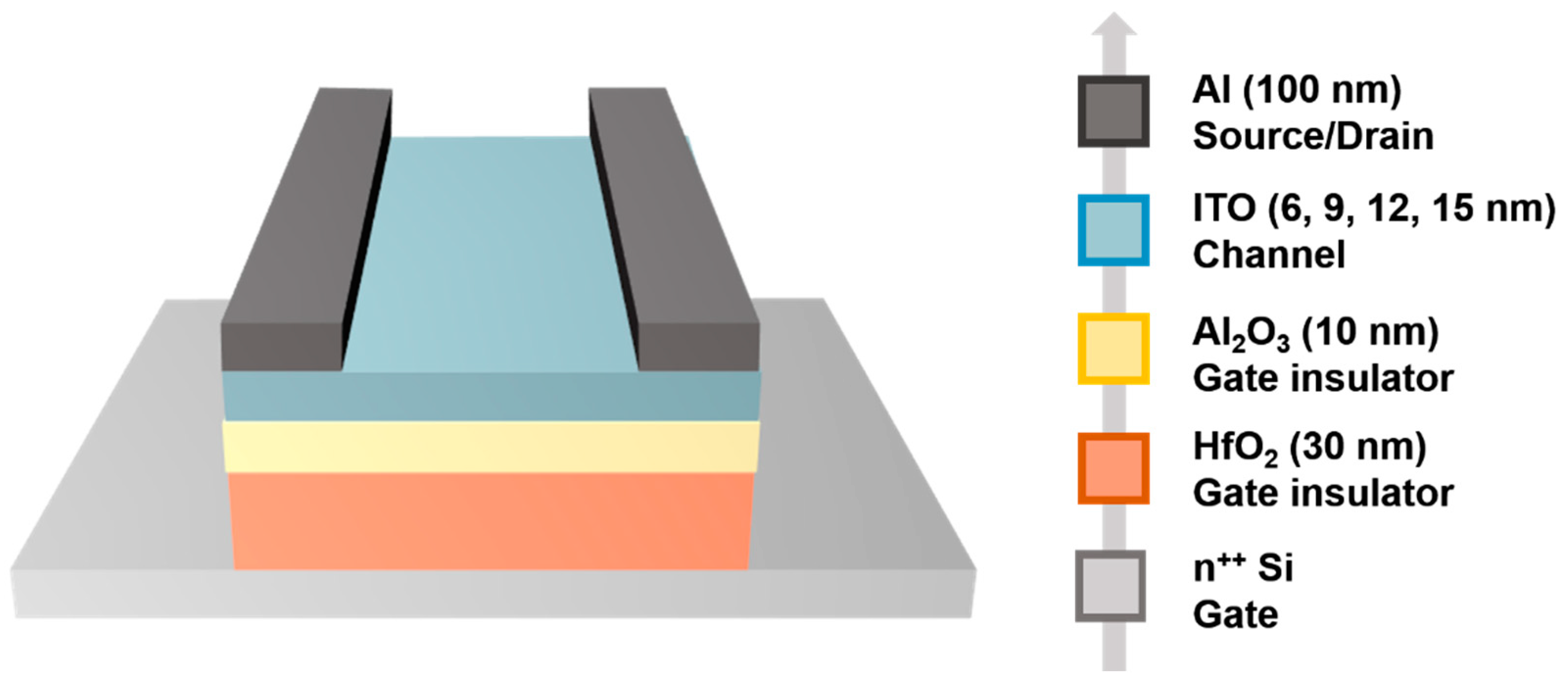
Figure 1 shows schematic structure of the ITO TFTs. Feature size of devices is width/length (W/L) = 100 μm/100 μm. Firstly, a heavily doped Si substrate was ultrasonic cleaned in acetone, alcohol, and deionized water, respectively. The Si substrate also acts as gate electrode. Next, a 30-nm HfO2 dielectric layer was deposited by sputtering process at room temperature. Then, a 10-nm Al2O3 dielectric layer was deposited by atomic layer deposition (ALD) process at 100 °C. Subsequently, an ITO channel layer was deposited by sputtering process, and the sputtering process was performed in Ar/O2 gas mixture (Ar/O2 flux ratio = 80/20) with a power of 70 W and a pressure of 1 Pa. Finally, a 100-nm Al source/drain electrode was deposited by sputtering process at room temperature. The ITO TFTs were patterned by lithography and lift-off processes. Before we measured device performance, the ITO TFTs were thermally annealed in vacuum at 100 °C for 1 h.
2.2. Characterization of ITO TFTs and ITO Films
Current-voltage (I-V) curves of the TFTs were characterized in dark at room temperature using a semiconductor parameter analyzer (Agilent B1500A). Capacitance properties of the metal–insulator–semiconductor (MIS) structure were measured using a semiconductor characterization system (Keithley 4200).
Microstructure of the ITO films were characterized by X-ray diffraction (XRD, Rigaku D/MAX 2000) and transmission electron microscopy (TEM, FEI Tecnai F20). Surface morphology of the ITO films were characterized by atomic force microscopy (AFM, Bruker Dimension Icon) and scanning electron microscope (SEM, FEI Helios Nanolab G3 CX). Chemical properties of the ITO thin films were examined using X-ray photoelectron spectroscopy (XPS, Axis Supra).
3. Results and Discussion
3.1. Material Characterization of ITO Films
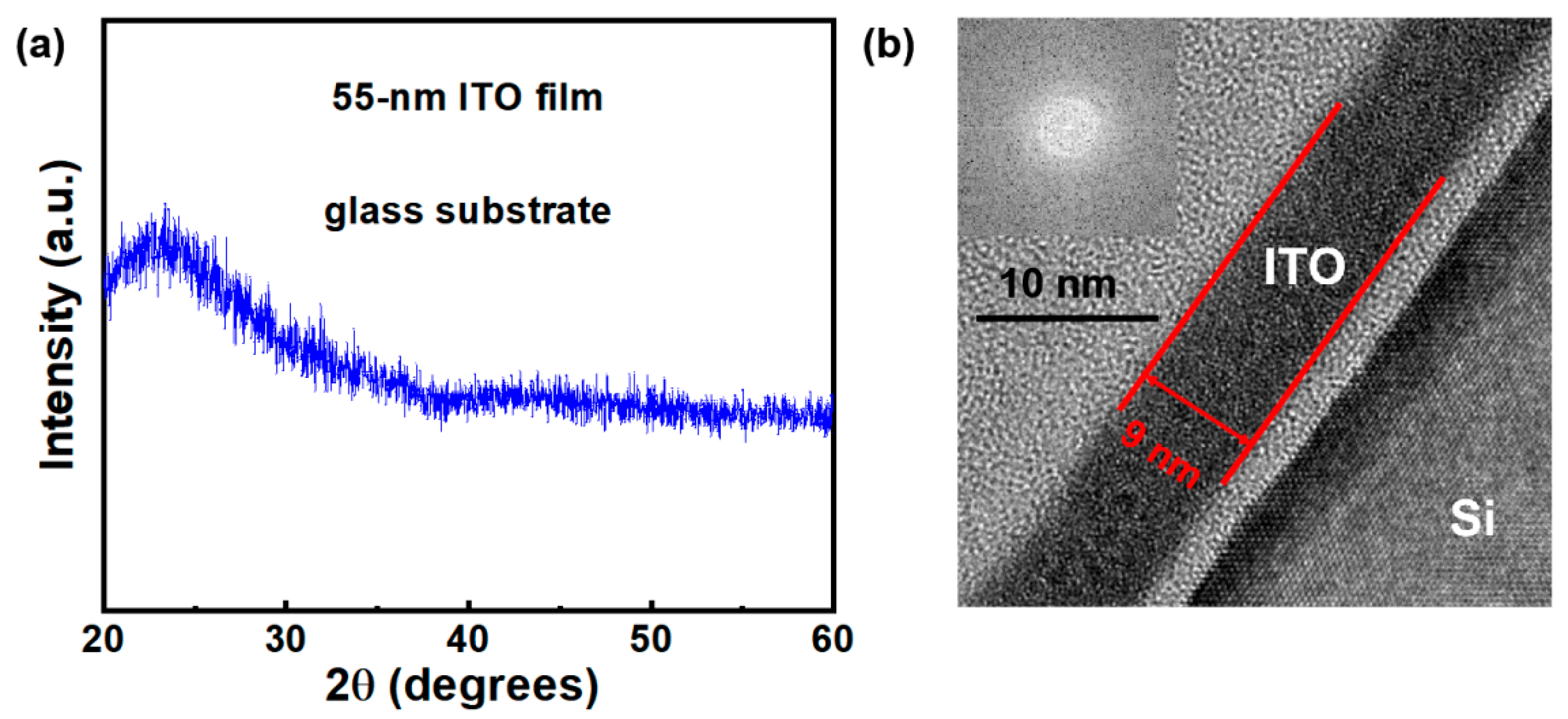
Figure 2a exhibits XRD spectrum of the ITO films. To accurately characterized diffraction peaks, the ITO films with a thickness of 55 nm were prepared on glass substrate. The obtained diffraction patterns contain only two broad peaks at approximately 23° and 45°, originating from the glass substrates [13]; this suggests that the ITO films have an amorphous phase. Normally, the amorphous phase of the ITO active layer is beneficial to the uniformity and stability of the ITO TFTs. In order to gain further insight into lattice structure of the ITO film, TEM measurement was performed, as shown in Figure 2b. It is observed that thickness of the ITO film is about 9 nm. No local crystalline grain can be observed. We performed real-time fast Fourier transform (FFT) of the ITO films, as shown in inset of Figure 2b. The FFT image exhibits amorphous diffraction pattern; thus, the lattice structure of the ITO film is definitely amorphous.
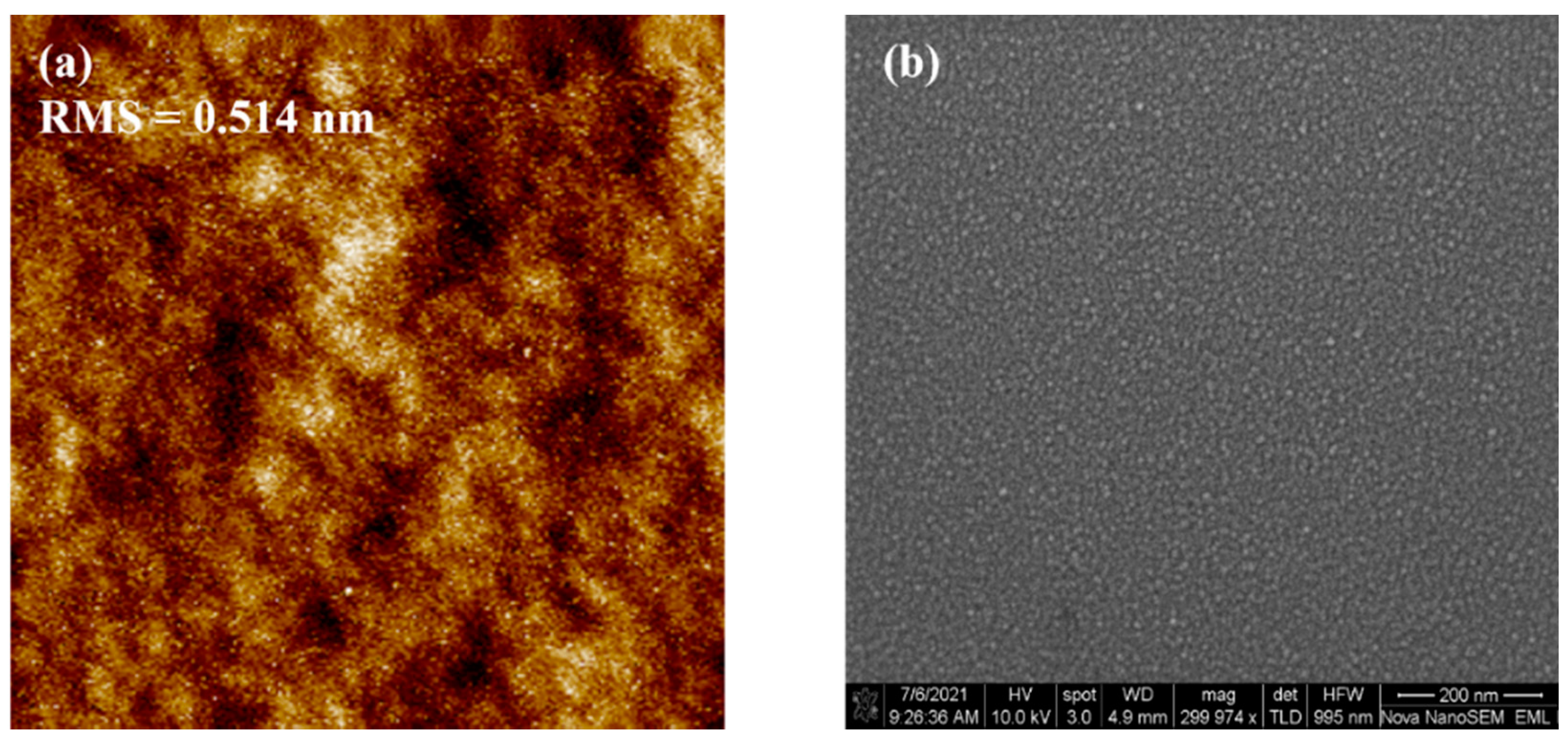
Figure 3a depicts AFM image of the ITO film, and the scanning area is set as 5 µm × 5 µm. Remarkably, the ITO film exhibits extremely flat surface morphology, and root-mean-square (RMS) roughness is 0.514 nm. Figure 3b shows SEM image of the ITO film. We can see that the local grains compactly and uniformly arrange with each other. The AFM and SEM validate smooth surface of the ITO films, which takes effect in reducing surface scattering and enhancing device performance of the ITO TFTs [14].
3.2. Electrical Characteristics of ITO TFTs
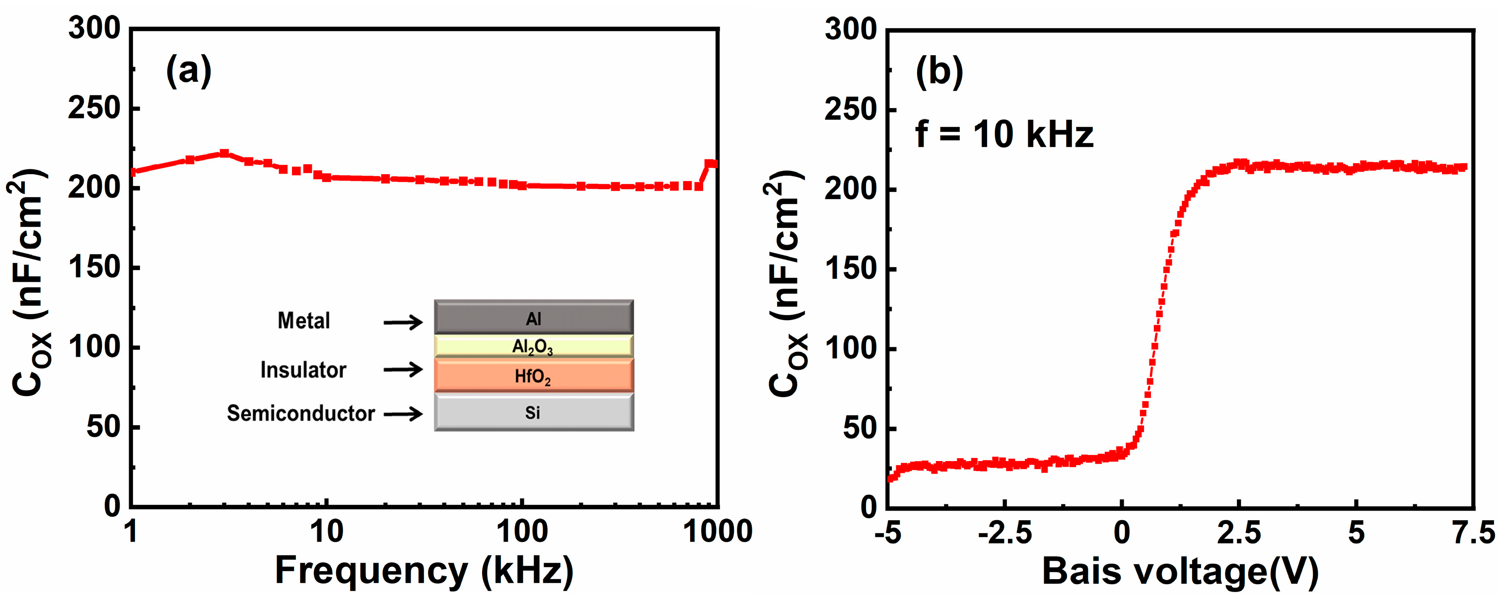
A MIS structure of Al-HfO2/Al2O3-Si was fabricated to determine capacitance properties. Fabrication process of the HfO2/Al2O3 bilayer dielectric is mentioned above. The Si substrate is n-type, lightly doped. Figure 4a exhibits the capacitance–frequency (C–F) curve of the MIS structure. Capacitance per unit area (COX) maintains a value of about 210 nF/cm2 with frequency from 1 KHz to 1 MHz, implying high film quality of the HfO2/Al2O3 bilayer dielectric. Figure 4b exhibits capacitance–voltage (C–V) curve of the MIS structure at a frequency of 10 KHz. The C–V curve exhibits typically high-frequency capacitance property. COX of the MIS structure is 214.55 nF/cm2 when voltage is 5 V, which is consistent with the C–F curve.
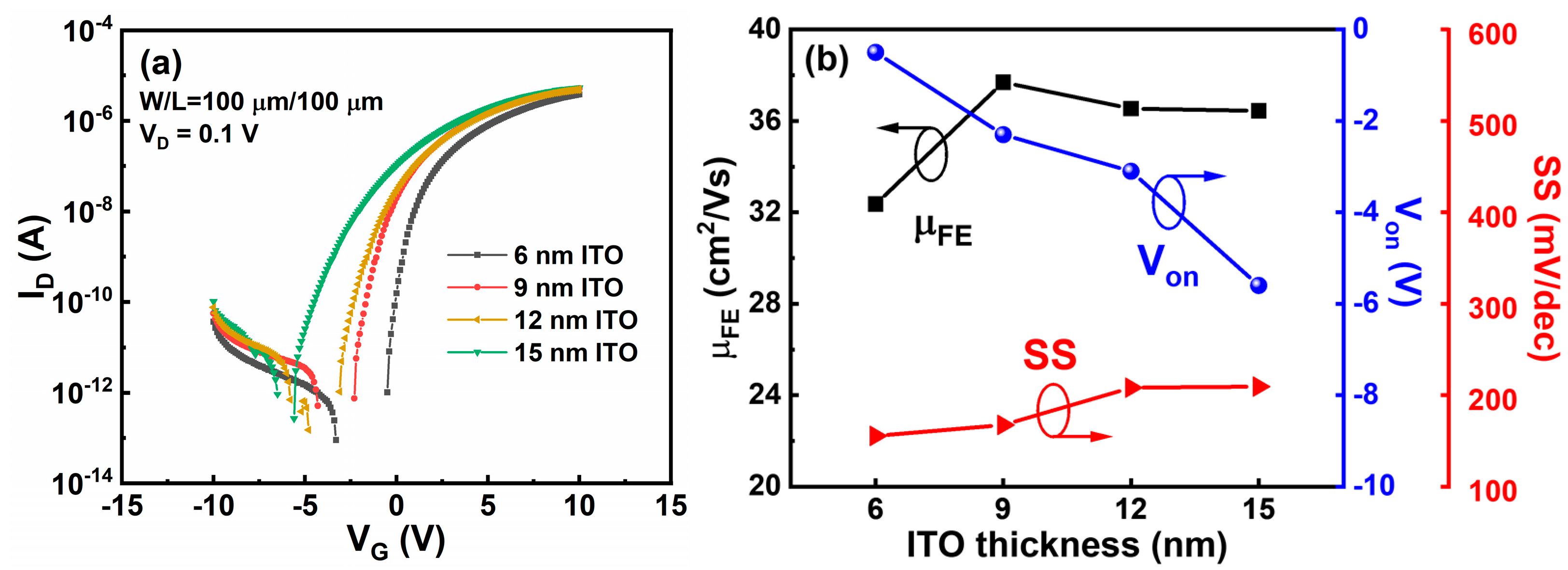
To examine effects of tITO on device performance of the ITO TFTs, drain current–gate voltage (ID–VG) curves were measured, as shown in Figure 5a. All of the devices show an on-state current (Ion) higher than 1 μA and an Ion/Ioff over 107. Electrical properties of μFE, Von, and SS are extracted, as shown in Figure 5b. Here, µFE is calculated using the following equation:
where L and W are channel length and channel width, respectively [15]. VD is drain voltage and is set as 0.1 V. SS is extracted from the linear part of a plot of the log (ID) versus VG, using SS = dVG/dlogID [16]. Von is defined as the gate voltage at which ID starts to monotonically increase [17]. We found that all of the devices show a μFE larger than 30 cm2/Vs. Notably, μFE reaches a peak value when tITO is 9 nm. Moreover, Von and SS present a negative and a positive correlation with tITO, and significant degeneration of Von and SS occurs as tITO increases to 12 and 15 nm, which results from large number of free electrons and higher sheet trap density in the channel layer [18,19]. Consequently, the ITO TFTs with 9-nm ITO active layer show the best electrical properties, such as a μFE of 37.69 cm2/Vs, a Von of −2.3 V, and a SS of 167.49 mV/decade.
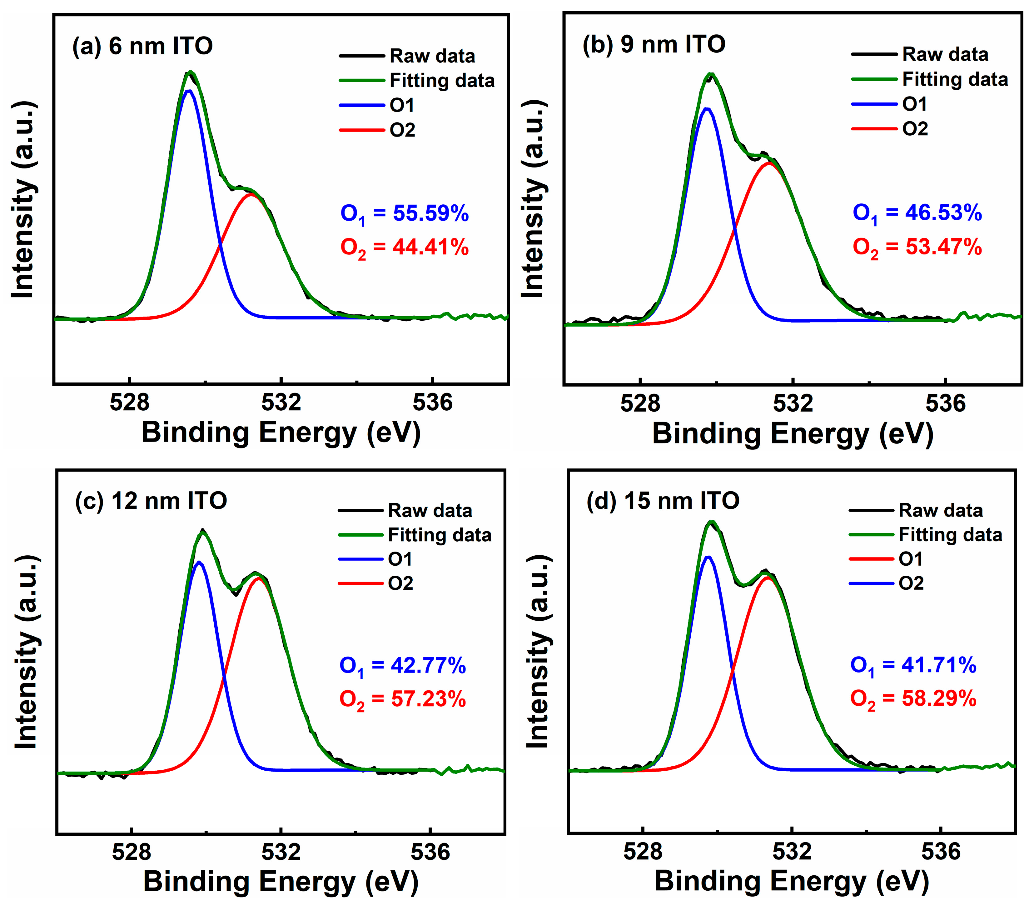
In order to deeply understand the physical mechanism behind the electrical performances of ITO TFTs, we characterized the ITO films with different thickness by XPS, as shown in Figure 6. The binding energy (BE) was calibrated by the standard C 1 s line at 284.80 eV [20]. The O 1 s peak is deconvoluted into two components: O1 peak at around 529.7 eV and O2 peak at around 531.3 eV, which can be regarded as metal–oxygen lattice and oxygen defects (oxygen vacancies and chemisorbed oxygen element), respectively [21]. Here, the ratio of oxygen defects is defined as the peak area ratio of O2/(O1 + O2) and is positively correlated with tITO. The oxygen defects can serve as interface traps; therefore, the SS is deteriorated with increasing tITO due to the increase of oxygen defects [22,23]. It is known that the content of oxygen vacancies, which normally acts as a shallow donor in oxide semiconductor, directly affects the carrier concentration of ITO films [1]. Consequently, the Von negatively shifts with increasing tITO and the μFE increases with tITO increasing from 6 to 9 nm. However, similar to other impurity dopants, more oxygen defects can induce more ionized impurity scattering, which possibly results in the degradation of μFE with tITO increasing from 9 to 15 nm [24].
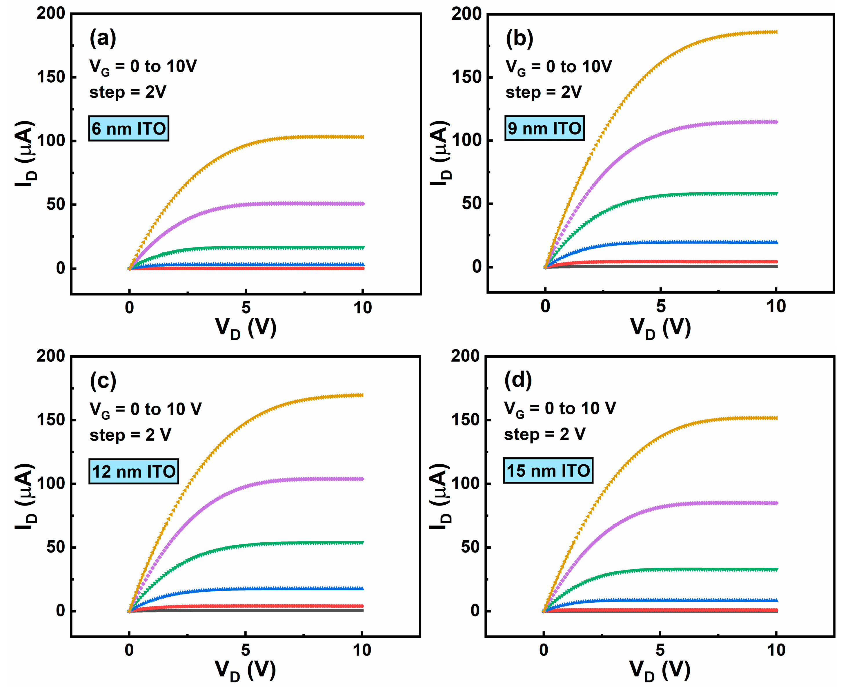
Drain current–drain voltage (ID-VD) curves of the ITO TFTs are measured, as shown in Figure 7a–d. All the ID–VD curves show apparent linear and saturation region. As tITO increases from 6 to 15 nm, the saturation current increases first and then decreases, and the maximum value of 184 µA is observed when tITO is 9 nm. Additionally, there is no obvious current crowding phenomenon for all the ITO TFTs, indicating good Ohmic contact between ITO channel layer and Al source/drain electrodes [25].
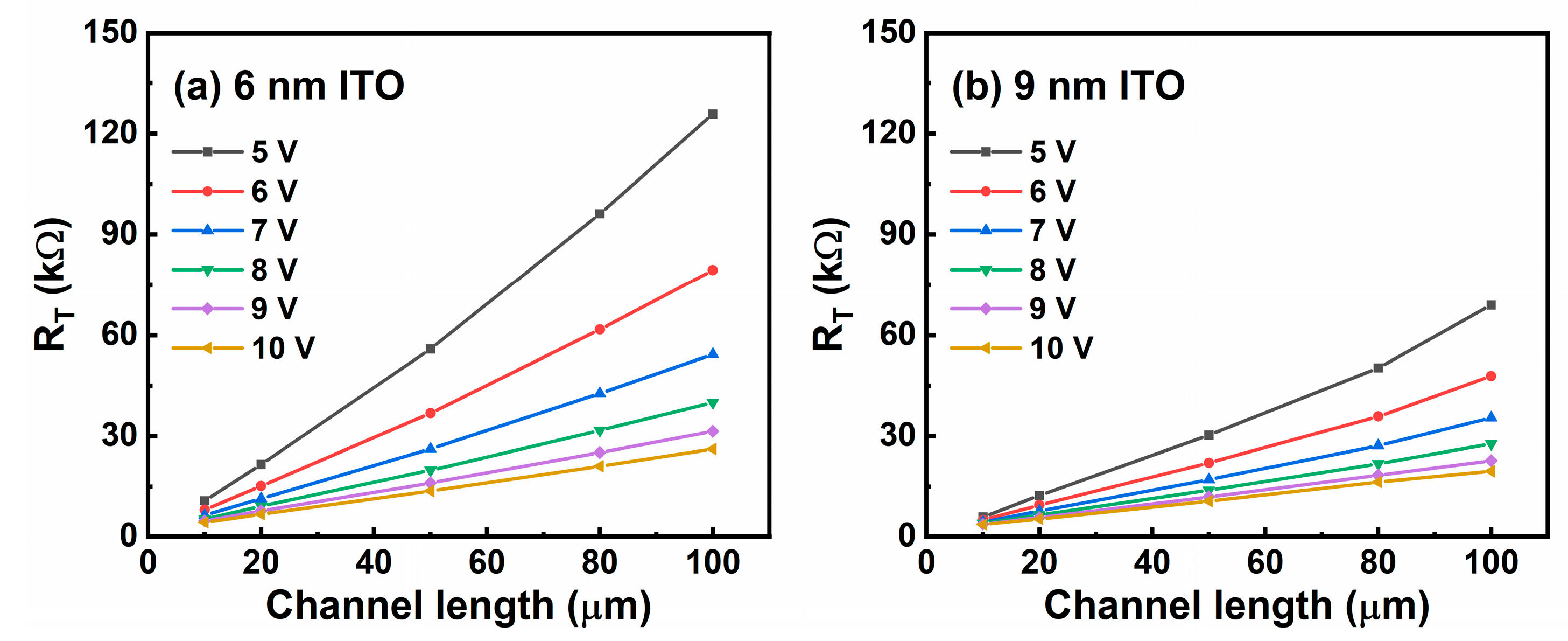
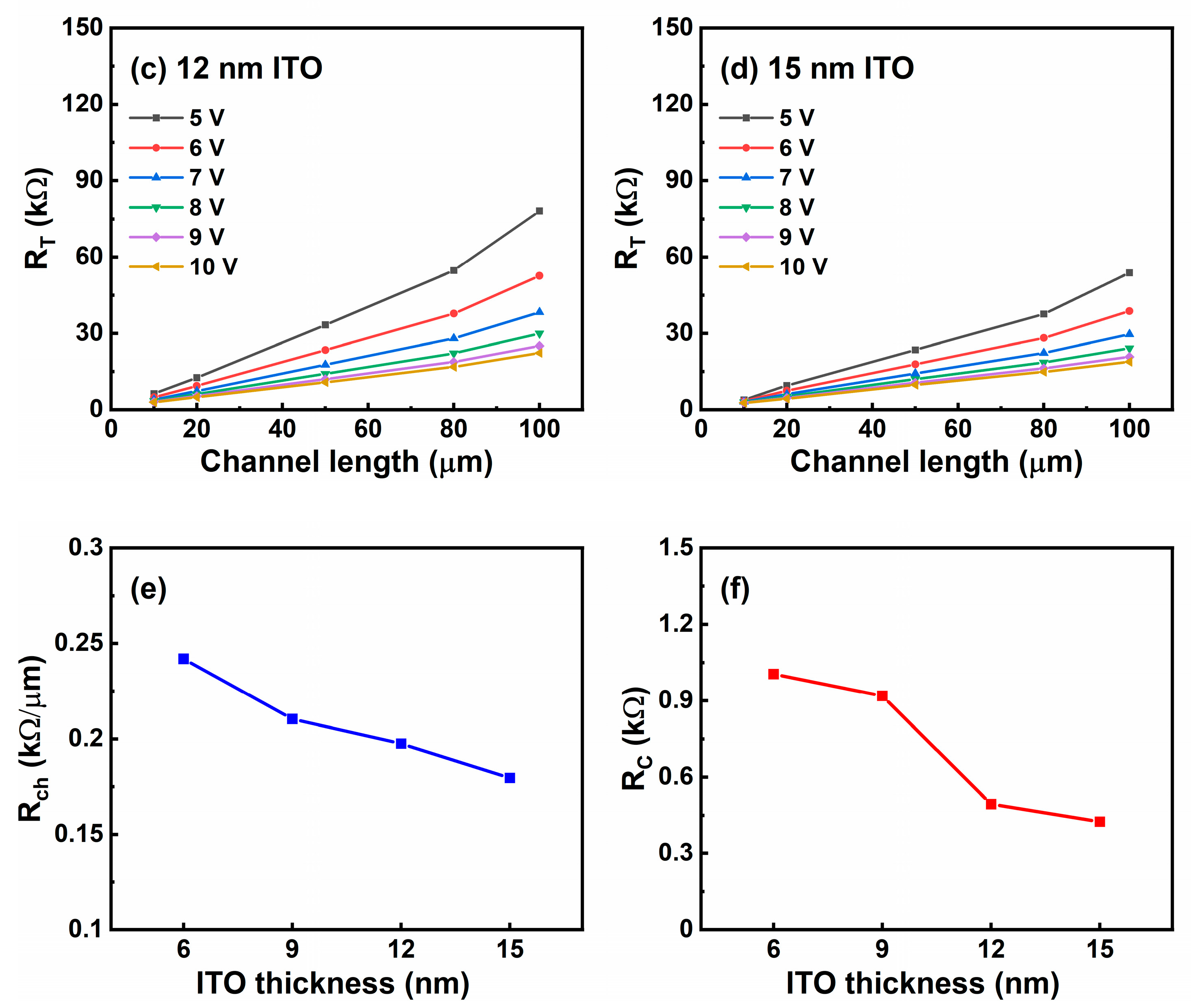
In order to comprehensively analyze contact property between ITO channel layer and Al source/drain electrode, we extract contact resistance (RC) based on transfer line method (TLM). Total resistance (RT) of the TFTs at on-state is expressed as RT = RchL + 2RC, where Rch and L represent channel resistance per unit length and channel length, respectively [26]. RT versus L at different VG for the ITO TFTs are shown in Figure 8a–d. By applying linear fitting, we obtain Rch and RC of the ITO TFTs, as shown in Figure 8e,f. Significantly, both Rch and RC present a negative correlation with tITO, which attributes to the increasing amount of conductive electrons in the ITO channel layers. Thereby, contact property can be enhanced by increasing tITO.
In the aspect of contact property, we found that increasing tITO plays a role in enhancing contact property of the ITO TFTs. Commonly, a preferable contact property is desirable for high-performance metal–oxide TFTs. However, we verify that Von and SS dramatically degrade when tITO increases to 12 and 15 nm (Figure 5b). μFE and saturation current achieve the maximum value when tITO is 9 nm. That is to say, an optimal tITO is 9 nm in this work.
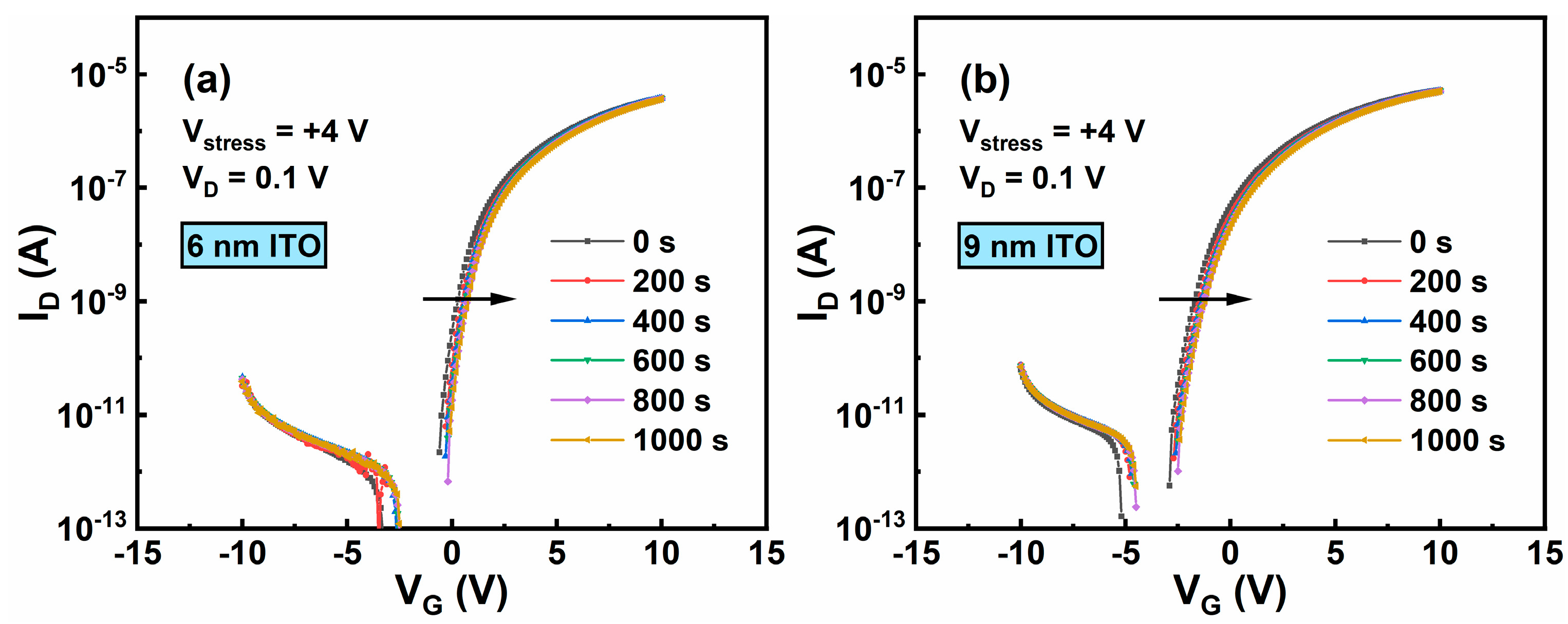
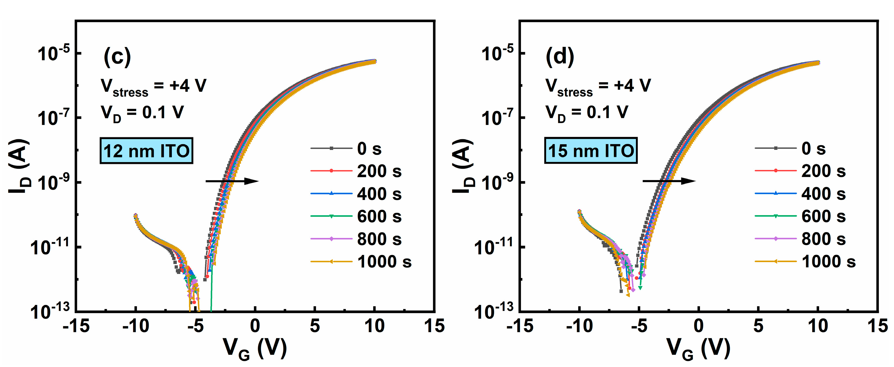
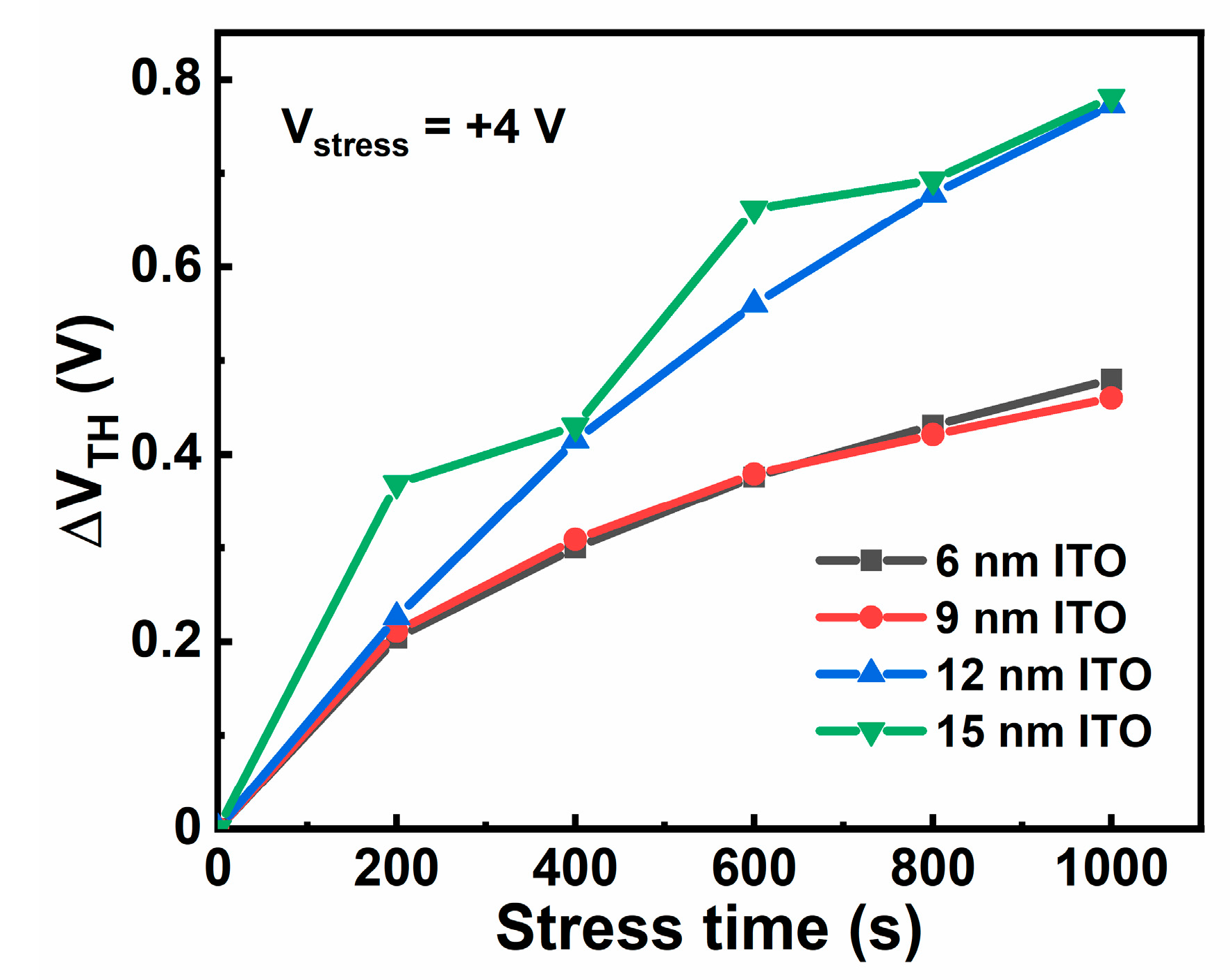
Finally, PBS stability of the ITO TFTs are measured, as shown in Figure 9a–d. Stress conditions are as follow: the stress voltage applied on the gate electrode is +4 V with the source and drain electrodes grounded, and the stress duration is 1000 s. Figure 10 presents ΔVTH of the ITO TFTs with different tITO under PBS at different stress times. In general, the devices show improved stability under PBS with reducing tITO, which is consistent with the previously reported results [27,28,29]. One possible mechanism related to PBS is the oxygen vacancy model [30]. As shown in Figure 6, for ITO TFT with a larger tITO, there are more oxygen vacancy defects, causing a larger positive ∆VTH.
4. Conclusions
In conclusion, high-performance, robust ITO TFTs are fabricated at a maximum process temperature of 100 °C. We investigate the effects of tITO on the electrical characteristics and PBS stability of ITO TFTs with tITO of 6, 9, 12, and 15 nm. We found that content of oxygen defects positively correlates with tITO, leading to increase of both trap states as well as carrier concentration, and synthetically determining electrical properties of the ITO TFTs. Interestingly, the devices with a 9-nm ITO thickness show the best performance with a large µFE of 37.69 cm2/Vs, a high Ion/Ioff over 107, a reasonable Von of −2.3 V, and a steep SS of 167.49 mV/decade. Moreover, the device exhibits preferable stability under PBS (∆VTH = 0.46 V). Overall, our ITO TFTs show great potential in next-generation displays.
Author Contributions
Q.L. and J.D. conceived and planned the experiments; Q.L. carried out the experiments; formal analysis, Q.L. and J.D.; writing—original draft, Q.L.; supervision, D.H. and Y.W.; resources, J.D., D.H. and Y.W. All authors have read and agreed to the published version of the manuscript.
Funding
This research was funded by the National Natural Science Foundation of China (Grant 62004003).
Institutional Review Board Statement
Not applicable.
Informed Consent Statement
Not applicable.
Data Availability Statement
The data that support the findings of this study are available from the corresponding author upon reasonable request.
Conflicts of Interest
The authors declare no conflict of interest.
References
- Kamiya, T.; Nomura, K.; Hosono, H. Origins of High Mobility and Low Operation Voltage of Amorphous Oxide TFTs: Electronic Structure, Electron Transport, Defects and Doping. J. Disp. Technol. 2009, 5, 273–288. [Google Scholar] [CrossRef]
- Fortunato, E.; Barquinha, P.; Martins, R. Oxide Semiconductor Thin-film transistors: A Review of Recent Advances. Adv. Mater. 2012, 24, 2945–2986. [Google Scholar] [CrossRef] [PubMed]
- Park, J.S.; Maeng, W.J.; Kim, H.S.; Park, J.S. Review of Recent Developments in Amorphous Oxide Semiconductor Thin-film Transistor Devices. Thin Solid Film. 2012, 520, 1679–1693. [Google Scholar] [CrossRef]
- Shi, J.; Zhang, J.; Yang, L.; Qu, M.; Qi, D.C.; Zhang, K.H.L. Wide Bandgap Oxide Semiconductors: From Materials Physics to Optoelectronic Devices. Adv. Mater. 2021, e2006230. [Google Scholar] [CrossRef] [PubMed]
- Goh, Y.; Ahn, J.; Lee, J.R.; Park, W.W.; Park, S.H.K.; Jeon, S. Efficient Suppression of Defects and Charge Trapping in High Density In-Sn-Zn-O Thin Film Transistor Prepared using Microwave-Assisted Sputter. ACS Appl. Mater. Interfaces 2017, 9, 36962–36970. [Google Scholar] [CrossRef]
- Kang, Y.; Lee, W.; Kim, J.; Keum, K.; Kang, S.H.; Jo, J.W.; Park, S.K.; Kim, Y.H. Effects of Crystalline Structure of IGZO Thin Films on the Electrical and Photo-stability of Metal-oxide Thin-film Transistors. Mater. Res. Bull. 2021, 139, 111252. [Google Scholar] [CrossRef]
- Kim, H.; Horwitz, J.S.; Kushto, G.; Piqué, A.; Kafafi, Z.H.; Gilmore, C.M.; Chrisey, D.B. Effect of Film Thickness on the Properties of Indium Tin Oxide Thin Films. J. Appl. Phys. 2000, 88, 6021–6025. [Google Scholar] [CrossRef]
- Granqvist, C.G.; Hultaker, A. Transparent and Conducting ITO Films: New Developments and Applications. Thin Solid Film. 2002, 411, 1–5. [Google Scholar] [CrossRef]
- Wang, Y.; Wang, Z.; Huang, K.; Liang, X.; Liu, C.; Chen, C.; Liu, C. Solution-processed ITO Thin-film Transistors With Doping of Gallium Oxide Show High On-off Ratios and Work at 1 mV Drain Voltage. Appl. Phys. Lett. 2020, 116, 141604. [Google Scholar] [CrossRef]
- Li, S.; Tian, M.; Gao, Q.; Wang, M.; Li, T.; Hu, Q.; Li, X.; Wu, Y. Nanometre-thin Indium Tin Oxide for Advanced High-performance Electronics. Nat. Mater. 2019, 18, 1091–1097. [Google Scholar] [CrossRef] [PubMed]
- Park, S.Y.; Ji, K.H.; Jung, H.Y.; Kim, J.-H.; Choi, R.; Son, K.S.; Ryu, M.K.; Lee, S.; Jeong, J.K. Improvement in the Device Performance of Tin-doped Indium Oxide Transistor by Oxygen High Pressure Annealing at 150 °C. Appl. Phys. Lett. 2020, 100, 162108. [Google Scholar] [CrossRef]
- Liang, K.; Li, D.; Ren, H.; Zhao, M.; Wang, H.; Ding, M.; Xu, G.; Zhao, X.; Long, S.; Zhu, S.; et al. Fully Printed High-Performance n-Type Metal Oxide Thin-Film Transistors Utilizing Coffee-Ring Effect. Nanomicro Lett. 2021, 13, 164. [Google Scholar] [CrossRef]
- Kim, D.H.; Cha, H.S.; Jeong, H.S.; Hwang, S.H.; Kwon, H.-I. Effects of Active Layer Thickness on the Electrical Characteristics and Stability of High-Mobility Amorphous Indium–Gallium–Tin Oxide Thin-Film Transistors. Electronics 2021, 10, 1295. [Google Scholar] [CrossRef]
- Choi, K.H.; Kim, H.K. Correlation between Ti Source/drain Contact and Performance of InGaZnO-based Thin Film Transistors. Appl. Phys. Lett. 2013, 102, 052103. [Google Scholar] [CrossRef] [Green Version]
- Lee, J.Y.; Lee, S.Y. Investigation on Hump Mechanism in Amorphous SiZnSnO Thin-Film Transistor Depending on Si Concentration. Phys. Status Solidi A 2020, 217, 1900953. [Google Scholar] [CrossRef]
- Teng, T.; Hu, C.-F.; Qu, X.-P.; Wang, M. Investigation of the Anomalous Hump Phenomenon in Amorphous InGaZnO Thin-film Transistors. Solid State Electron. 2020, 170, 107814. [Google Scholar] [CrossRef]
- Li, H.; Han, D.; Dong, J.; Yi, Z.; Zhou, X.; Zhang, S.; Zhang, X.; Wang, Y. Enhanced Performance of Atomic Layer Deposited Thin-Film Transistors With High-Quality ZnO/Al2O3 Interface. IEEE Trans. Electron. Devices 2020, 67, 518–523. [Google Scholar] [CrossRef]
- Barquinha, P.; Pimentel, A.; Marques, A.; Pereira, L.; Martins, R.; Fortunato, E. Influence of the semiconductor thickness on the electrical properties of transparent TFTs based on indium zinc oxide. J. Non-Cryst. Solids 2006, 352, 1749–1752. [Google Scholar] [CrossRef]
- Park, H.-W.; Park, K.; Kwon, J.-Y.; Choi, D.; Chung, K.-B. Effect of active layer thickness on device performance of tungsten-doped InZnO thin-film transistor. IEEE Trans. Electron. Dev. 2016, 64, 159–163. [Google Scholar] [CrossRef]
- Barreca, D.; Garon, S.; Tondello, E.; Zanella, P. SnO2 Nanocrystalline Thin Films by XPS. Surf. Sci. Spectra 2000, 7, 81–85. [Google Scholar] [CrossRef]
- Li, Y.; Yao, R.; Wang, H.H.; Wu, X.M.; Wu, J.Z.; Wu, X.H.; Qin, W. Enhanced Performance in Al-doped ZnO Based Transparent Flexible Transparent Thin-film Transistors Due to Oxygen Vacancy in ZnO Film With Zn-Al-O Interfaces Fabricated by Atomic Layer Deposition. ACS Appl. Mater. Interfaces 2017, 9, 11711–11720. [Google Scholar] [CrossRef]
- Kwon, S.; Bang, S.; Lee, S.; Jeon, S.; Jeong, W.; Kim, H.; Gong, S.C.; Chang, H.J.; Park, H.; Jeon, H. Characteristics of the ZnO Thin Film Transistor by Atomic Layer Deposition at Various Temperatures. Semicond. Sci. Technol. 2009, 24, 035015. [Google Scholar] [CrossRef]
- Wang, Y.H.; Ma, Q.; Zheng, L.L.; Liu, W.J.; Ding, S.J.; Lu, H.L.; Zhang, D.W. Performance Improvement of Atomic Layer-deposited ZnO/Al2O3 Thin-film Transistors by Low-temperature Annealing in Air. IEEE Trans. Electron. Devices 2016, 63, 1893–1898. [Google Scholar] [CrossRef]
- Liu, L.C.; Chen, J.S.; Jeng, J.S. Ambient Constancy of Passivation-Free Ultra-Thin Zinc Tin Oxide Thin Film Transistor. ECS Solid State Lett. 2015, 4, Q59–Q62. [Google Scholar] [CrossRef]
- Jeon, S.R.; Song, Y.H.; Jang, H.J.; Yang, G.M.; Hwang, S.W.; Son, S.J. Lateral Current Spreading in GaN-based Light-emitting Diodes Utilizing Tunnel Contact Junctions. Appl. Phys. Lett. 2001, 78, 3265–3267. [Google Scholar] [CrossRef]
- Campbell, J.P.; Cheung, K.P.; Suehle, J.S.; Oates, A. A Simple Series Resistance Extraction Methodology for Advanced CMOS Devices. IEEE Electron. Device Lett. 2011, 32, 1047–1049. [Google Scholar] [CrossRef]
- Yang, Z.; Yang, J.W.; Meng, T.; Qu, M.Y.; Zhang, Q. Influence of Channel Layer Thickness on the Stability of Amorphous Indium Zinc Oxide Thin Film Transistors. Mater. Lett. 2016, 166, 46–50. [Google Scholar] [CrossRef]
- Ahn, C.H.; Yun, M.G.; Lee, S.Y.; Cho, H.K. Enhancement of Electrical Stability in Oxide Thin-film Transistors Using Multilayer Channels Grown by Atomic Layer Deposition. IEEE Trans. Electron. Devices 2014, 60, 73–78. [Google Scholar] [CrossRef]
- Li, J.; Ding, X.W.; Zhang, J.H.; Zhang, H.; Jiang, X.Y.; Zhang, Z.L. Improving Electrical Performance and Bias Stability of HfInZnO-TFT With Optimizing the Channel Thickness. AIP Adv. 2013, 3, 102132. [Google Scholar] [CrossRef]
- Zhou, X.B.; Han, D.D.; Dong, J.C.; Li, H.J.; Yi, Z.; Zhang, X.; Wang, Y. The Effects of Post Annealing Process on the Electrical Performance and Stability of Al-Zn-O Thin-Film Transistors. IEEE Electron. Device Lett. 2020, 41, 569–572. [Google Scholar] [CrossRef]
Figure 1.
Schematic device structure and device fabrication procedure of ITO TFTs.

Figure 2.
(a) XRD spectrum of ITO film on glass substrate. Film thickness is 55 nm. (b) TEM image and FFT image of ITO film.
Figure 2.
(a) XRD spectrum of ITO film on glass substrate. Film thickness is 55 nm. (b) TEM image and FFT image of ITO film.

Figure 3.
(a) AFM image of the ITO film. Scanning area is 5 µm × 5 µm. (b) SEM image of ITO film. Film thickness is 9 nm.
Figure 3.
(a) AFM image of the ITO film. Scanning area is 5 µm × 5 µm. (b) SEM image of ITO film. Film thickness is 9 nm.

Figure 4.
(a) C–F curve of the MIS structure. (b) C–V curve of the MIS structure. Frequency is 10 KHz.
Figure 4.
(a) C–F curve of the MIS structure. (b) C–V curve of the MIS structure. Frequency is 10 KHz.

Figure 5.
(a) Transfer curves of ITO TFTs. VD = 0.1 V. (b) Electrical parameters of ITO TFTs, including μFE, Von, and SS.
Figure 5.
(a) Transfer curves of ITO TFTs. VD = 0.1 V. (b) Electrical parameters of ITO TFTs, including μFE, Von, and SS.

Figure 6.
Deconvolution of the O 1 s XPS spectrum of ITO films with thickness of (a) 6 nm, (b) 9 nm, (c) 12 nm, and (d) 15 nm.
Figure 6.
Deconvolution of the O 1 s XPS spectrum of ITO films with thickness of (a) 6 nm, (b) 9 nm, (c) 12 nm, and (d) 15 nm.

Figure 7.
Output characteristics of ITO TFTs with tITO of (a) 6 nm, (b) 9 nm, (c) 12 nm, and (d) 15 nm.
Figure 7.
Output characteristics of ITO TFTs with tITO of (a) 6 nm, (b) 9 nm, (c) 12 nm, and (d) 15 nm.

Figure 8.
Total resistance (RT) of ITO TFTs with tITO of (a) 6 nm, (b) 9 nm, (c) 12 nm, and (d) 15 nm. (e) Rch and (f) RC as a function of tITO.
Figure 8.
Total resistance (RT) of ITO TFTs with tITO of (a) 6 nm, (b) 9 nm, (c) 12 nm, and (d) 15 nm. (e) Rch and (f) RC as a function of tITO.


Figure 9.
PBS (VG = +4 V) of ITO TFTs with tITO of (a) 6 nm, (b) 9 nm, (c) 12 nm, and (d) 15 nm.


Figure 10.
∆VTH for the ITO TFTs with different tITO under PBS at different stress times.

Publisher’s Note: MDPI stays neutral with regard to jurisdictional claims in published maps and institutional affiliations. |
© 2021 by the authors. Licensee MDPI, Basel, Switzerland. This article is an open access article distributed under the terms and conditions of the Creative Commons Attribution (CC BY) license (https://creativecommons.org/licenses/by/4.0/).
Share and Cite
MDPI and ACS Style
Li, Q.; Dong, J.; Han, D.; Wang, Y. Effects of Channel Thickness on Electrical Performance and Stability of High-Performance InSnO Thin-Film Transistors. Membranes 2021, 11, 929. https://doi.org/10.3390/membranes11120929
AMA Style
Li Q, Dong J, Han D, Wang Y. Effects of Channel Thickness on Electrical Performance and Stability of High-Performance InSnO Thin-Film Transistors. Membranes. 2021; 11(12):929. https://doi.org/10.3390/membranes11120929
Chicago/Turabian StyleLi, Qi, Junchen Dong, Dedong Han, and Yi Wang. 2021. "Effects of Channel Thickness on Electrical Performance and Stability of High-Performance InSnO Thin-Film Transistors" Membranes 11, no. 12: 929. https://doi.org/10.3390/membranes11120929
Note that from the first issue of 2016, this journal uses article numbers instead of page numbers. See further details here.