Effect of the Sputtering Power on the Structure, Morphology and Magnetic Properties of Fe Films


1
School of Materials Science and Engineering, Tongji University, Shanghai 201804, China
2
Shanghai key Laboratory for D&A of Metal functional Materials, Shanghai 201804, China
*
Author to whom correspondence should be addressed.
Metals 2020, 10(7), 896; https://doi.org/10.3390/met10070896
Submission received: 11 June 2020
/
Revised: 28 June 2020
/
Accepted: 30 June 2020
/
Published: 5 July 2020
(This article belongs to the Special Issue Advanced Magnetic Materials)
Abstract
:In this paper, the radio frequency (RF) magnetron sputtering (MS) method was utilized to fabricate multiple sets of the iron film samples under different sputtering powers. With the help of X-ray diffraction (XRD), scanning electron microscopy (SEM), atomic force microscopy (AFM) and vibrating sample magnetometer (VSM), how the sputtering power affected the structure, morphology and magnetic properties of the iron film was studied. XRD results showed that all Fe films have a polycrystalline bcc structure and (110) preferred orientation. According to the Bragg equation calculation, the larger the sputtering power, the larger the average grain size, which is consistent with the results of AFM particle size analysis. The main reason is that the sputtering power affects the grain growth mode. As the sputtering power increases, it gradually changes from a small island-like growth to a thick columnar growth. However, from the surface morphology and height profile, we saw that the iron film deposited under 230 W had the most uniform grain size distribution and the grain size was relatively small. This is why thin films deposited under this condition have the best soft magnetic properties. The saturation magnetization (Ms) reaches 1566 emu/cm3, coercivity (Hc) is 112 Oe, and squareness ratio (Mr/Ms) is 0.40. Therefore, iron film prepared under 230 W has good comprehensive properties (highest Ms, lower Hc and Mr/Ms) that provide an experimental basis for further thin film research work.
1. Introduction
Iron-based thin films are interesting because of their high saturation magnetization (Ms) and low coercivity (Hc) [1], which can be achieved by appropriate preparation processes. Therefore, it has huge application prospects in many fields, such as magnetic recording, magnetic storage, magnetoresistive sensing, electromagnetic switches, magnetic shielding, spin semiconductors and other electronic devices [2,3,4,5]. In order to realize the control of the performance of the iron thin film, researchers have carried out a lot of research work. The application of a high magnetic field during film growth can affect the grain size, regulate the growth direction of the columnar crystal, prevent grain overlap and the bending of columns, increase the saturation magnetization [2,6,7], and achieve vertical anisotropy [8]. Changing the film composition, such as adding SiO2, can effectively reduce the coercive force of the iron film and achieve vertical anisotropy, but will simultaneously reduce the saturation magnetization [6]; adding N and Co can improve the film saturation magnetization, resistivity and high frequency permeability [9]. An argon ion beam can effectively control the magnetic anisotropy of the sputtered film [10]. After iron ion irradiation, the lattice constant and grain size increase, and the magnetic moment of the top sublayer of the film is higher than the bottom sublayer, which can effectively adjust the film structure and magnetic properties [11]. An annealing treatment can change the texture of the film [12], reduce the coercive force and optimize the soft magnetic properties [2]; if heat-treated in a hydrogen atmosphere, oxygen-free and silicon-free interfaces can be prepared to modify the ferromagnetic film structure and magnetic properties [13]. These measures can achieve the optimization or adjustment of the magnetic properties of the thin film, but it will bring certain undesirable effects. That is, applying an external magnetic field or ion irradiation will destroy the film surface and enhance the complexity of the process and the difficulty of preparation; the doping of non-magnetic elements will reduce the magnetization of the film.
Adjusting the growth parameters is the most basic and effective optimization method in the thin film deposition process. Serizawa et al. [14] chose different types of substrates to grow iron thin films with different crystal orientations in order to adjust the magnetostrictive behavior. Gao et al. [15] controlled the substrate temperature to improve the morphology of the iron film. Cheng et al. [16] studied the dependence of the magnetic crystal anisotropy of iron films on temperature by adjusting the deposition time and controlling the film thickness. Javed et al. [17] found that the partial pressure of argon gas has a great influence on the soft magnetic properties of iron thin films prepared by DC magnetron sputtering. Brajpuriya et al. [1] found that when the iron film thickness is below a certain critical thickness (3 nm), it exhibits superparamagnetism; above this critical thickness, it exhibits ferromagnetism. Getman et al. [18] found that the grain size and grain aspect ratio will increase as the thickness (in the range of 0.1–1 μm) increases and will show the easy magnetization axis in the plane. Bourzami et al. [19] found that when the thickness is thin (48 nm), the coercive force decreases slightly as the thickness increases. When the threshold is exceeded, the coercive force increases as the film thickness increases; Tripathi et al.’s study further verified this conclusion [20]. Regarding the research on iron thin films, most of them focus on the deposition time (thickness) [21], growth temperature [22], substrate selection, etc. There are few reports pertaining to the influence of the sputtering power on the structure, morphology and magnetic properties of iron thin films [17,23].
However, in the film preparation process, the sputtering power has a profound influence on the film morphology, structure and performance. For example, the sputtering power affects the magnetic anisotropy of BiFeO3-CoFe2O4 nanocomposite films [24]. The sputtering power also affects the surface morphology, grain size and grain growth of Co2FeSi thin films, which affects the soft magnetic properties of the thin film [25]. The coercive force of TbFeCo thin films can be tailored by changing the sputtering power [26]. Increasing the sputtering power changes the magnetic behavior of the Tb-Fe thin film from superparamagnetic to ferromagnetic [27]. Sputtering power can affect both the composition of Co2FeSi thin films and the magnetization behavior either under zero field cooling or field cooling conditions [28]. Further, the sputtering power can change the transition temperature of the Co-Fe-Zr-B amorphous thin film, affect the amorphous forming ability of the thin film and then affect the soft magnetic properties [29]. Increasing the sputtering power can effectively improve the crystallinity of NiO film [30]. There is an optimal sputtering power where the ZnO-based thin film has optimal transparency and resistivity [31,32,33]. Adjusting the sputtering power can induce changes in the optical and electrical properties of CdO thin films [34]. The sputtering power can adjust the phase composition in the cobalt oxide film, thereby affecting the structure and performance [35]. The sputtering power can affect the growth rate and film thickness of Mo film, thereby affecting the electrical properties of the film [36]. Adjusting the sputtering power can optimize the magnetostrictive properties of Fe62Co19Ga19 thin films [37]. This research work indicates that it is necessary to carry out the influence of the sputtering power on the structure, morphology and magnetic properties of the iron thin film.
In this paper, the effect of the sputtering power on the structure, morphology and magnetic properties of the iron film prepared by radio frequency (RF) magnetron sputtering was studied. The purpose of this work was to reveal the relationship between the film growth parameters and the structure and performance of the film. Optimizing the thin film deposition process also lays the experimental foundation for the later research on the iron/semiconductor interface structure and magnetic properties.
2. Experimental Methods
The Fe films were deposited on glass substrates by RF magnetron sputtering method. Glass was used as the deposition substrate because there is greater diffusion between the iron thin film and the single crystal silicon substrate, which is not conducive to the magnetic properties of the iron thin film. A high-purity iron plate (Ø 60, 99.99%) was used as the sputtering target (Zhongnuo Advanced Material (Beijing) Technology Co., Ltd, Beijing, China). The glass substrate was ultrasonically cleaned twice in absolute ethanol and an acetone solution for 5 min each time. After removing the surface grease, it was placed in the chamber. In order to reduce the oxidation of the film, the vacuum chamber was evacuated to a basic pressure of about 7.5 × 10⁻⁵ Pa. We adjusted the argon flow rate and the working pressure until the glow discharge was stable, and then started to deposit the film. It was found in the experiment that when the working pressure was too low, the target could not generate glow discharge; when the working pressure was too high, the sputtering rate decreased and the film roughness increased. To ensure the deposition efficiency, we chose the lowest working pressure (3.5 Pa) and argon flow rate (29.9 sccm) at which glow discharge can occur and the deposition temperature of 25 °C. Prior to deposition, pre-sputtering was performed with the aim of cleaning the surface impurities of the Fe target and the time was determined by the target placement time. The distance between the substrate and target was 40 mm. By adjusting the current (0–500 mA) to control the sputtering power, a series of thin film samples were prepared under different sputtering powers. When the film was thin (below 200 nm), due to the influence of the substrate, the Ms of the film increased with the increase of the thickness; when the film thickness increased to a certain extent, the Ms of the film did not change greatly. Therefore, we selected a series of thin films with a deposition time of 20 min as the research object to illustrate the effect of the sputtering power on the film structure and magnetic properties.
The iron film thickness was measured employing scanning electron microscopy (SEM) (Nova NanoSEM 450, FEI, Portland, Oregon, USA). The crystal structure of the Fe films was determined with an applied X-ray diffraction (XRD) (DX-2007, Dandong fangyuan Co., Ltd, Dandong, China) carried out at 30 kV and 30 mA with Cu-Kα radiation. The magnetic properties of the Fe films were detected utilizing a vibrating sample magnetometer (VSM) (Model 7407, Lakeshore, Westerville, OH, USA). The film micromorphology and surface roughness were observed using atomic force microscopy (AFM) (Dimension Icon, Bruker, Billerica, MA, USA). All tests were performed at room temperature.
3. Results and Discussion
3.1. Crystal Structure
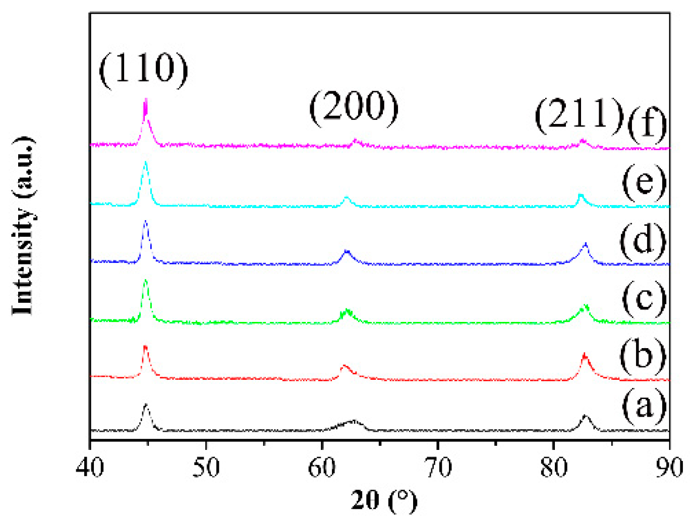
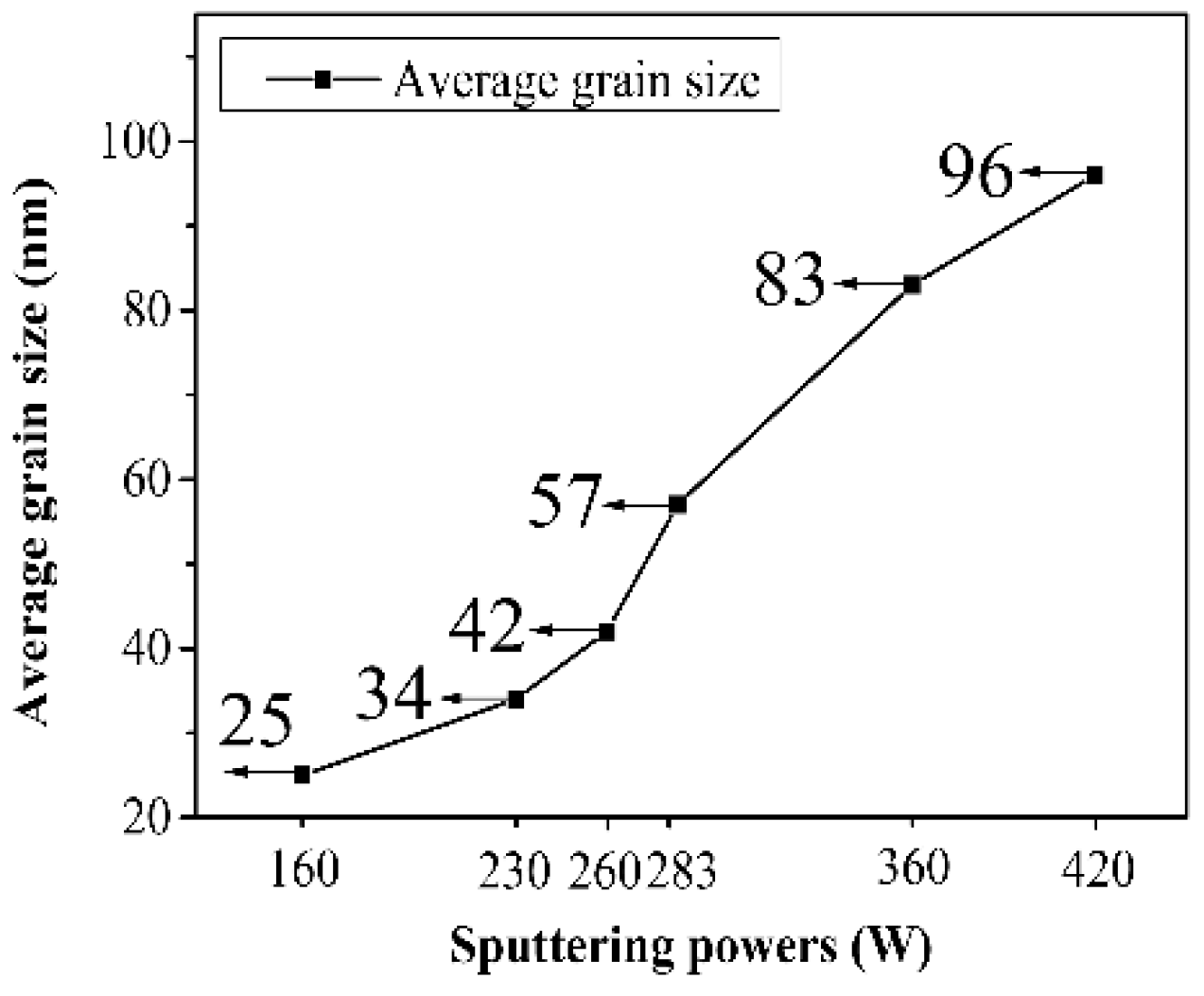
Figure 1 shows the XRD patterns of the Fe films prepared under different sputtering powers. For all samples, the characteristic Bragg reflections corresponding to (110) Fe, (200) Fe and (211) Fe were observed, exhibiting the polycrystalline nature of the Fe films. According to the Scherrer formula [38], the average grain size was calculated. These indicated that the average grain size of the Fe films monotonously increased with the sputtering power, as illustrated in Figure 2. This is mainly due to the fact that the change of the sputtering power affected the Fe film’s growth mode, as explained in the cross-sectional morphology of the films.
3.2. Cross-Sectional Morphology
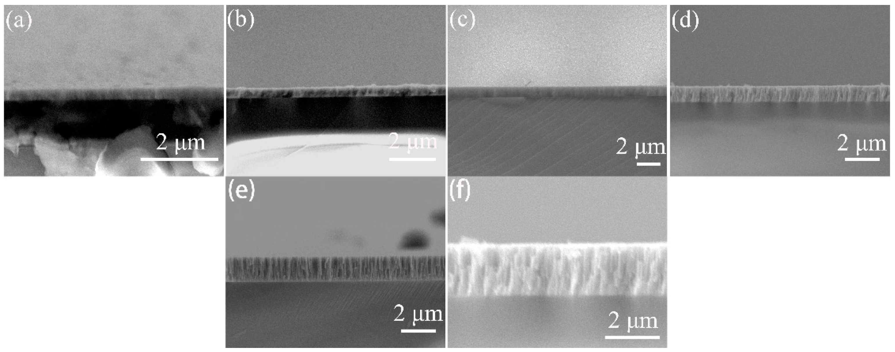
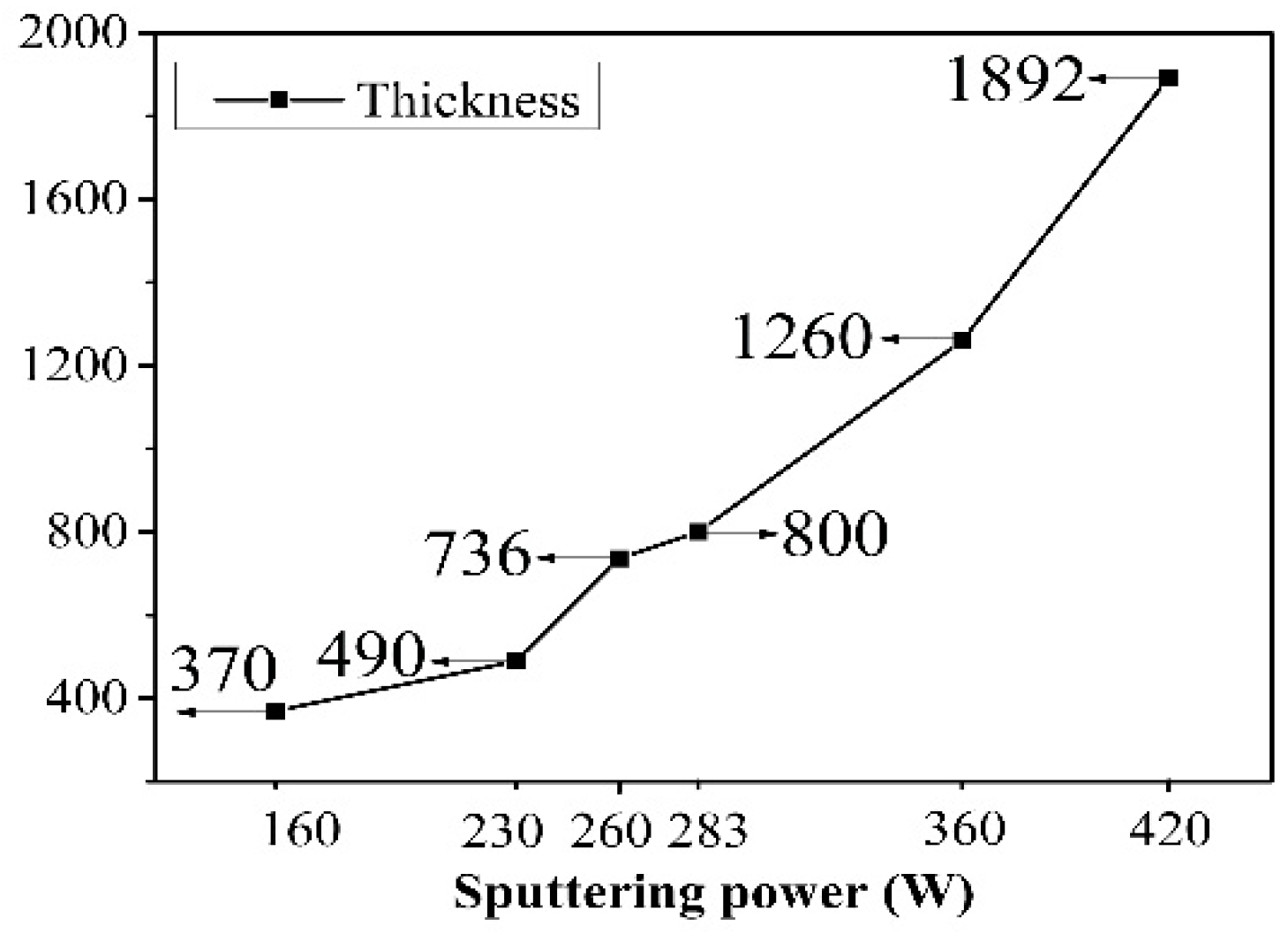
Figure 3 exhibits the cross-sectional SEM views of Fe films fabricated with different sputtering powers. The thickness of the Fe films deposited at 160 W, 230 W, 283 W, 360 W was measured to be the following: 370 nm, 490 nm, 800 nm, 1260 nm. The thickness of the films exhibited a linear increase with the sputtering powers, as illustrated in Figure 4. This is mainly because the greater the sputtering power, the stronger the field strength between electrons. As a result, the number of the sputtered particle increased, related to the larger avalanche multiplication effect [39,40]. This led to the increase in the sputtering rate. Under the same sputtering time, the faster the sputtering rate, the greater the thickness of the film [41].
By comparing the cross-sectional morphology of the Fe films prepared under different sputtering powers, we found that the Fe films with a sputtering power of 360 W exhibited a columnar growth structure perpendicular to the glass substrate and coarse grain. Dissimilarly, the Fe films sputtered at 160 W and 230 W showed a fine fibrous structure; the Fe film at 283 W was in the transition phase of a columnar structure. When the sputter power was low, the incident ion energy was lower. As a result, the diffusion ability of the atomic surface was limited and the critical core size required for thin film nucleation was very small. Therefore, the film tended to form more nucleation cores and have a finer grain size. On the contrary, when the sputter power was high, the atomic diffusion on the surface of the film was sufficient and showed columnar and coarse grain [2].
3.3. Surface Morphology
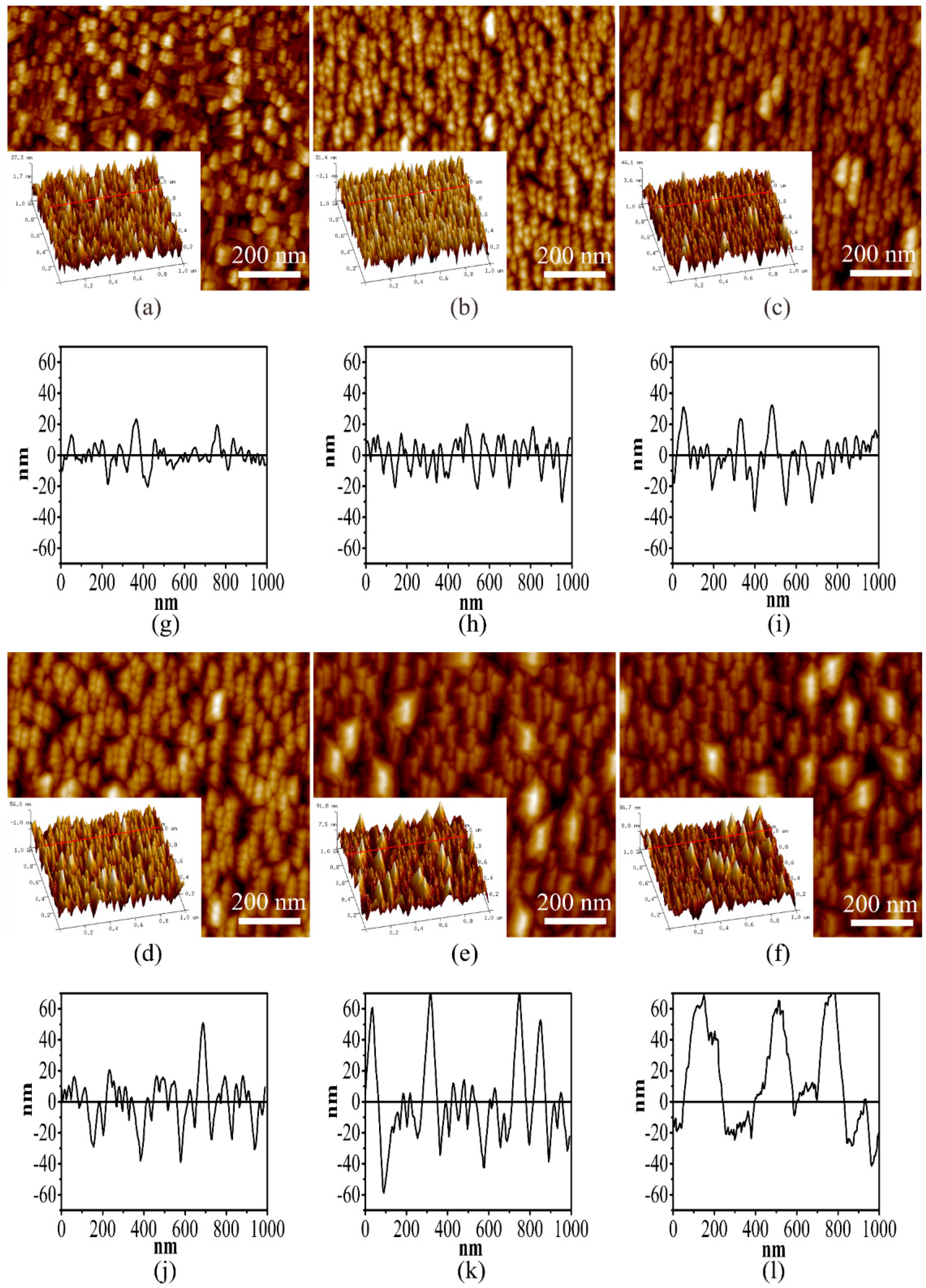
The surface morphology with the three-dimensional-view located at the bottom-left of the figure measured by AFM is displayed in Figure 5a–f. It can be observed that there were some pronounced surface morphology changes for the Fe films deposited at different sputtering powers. For the films at 160 W, the grains grew and gathered to the rambling and cuboid-like particles. A large number of the inclined cuboid-like particles increased the disorder degree of the film structure. The low sputtering energy was not enough to form a columnar growth completely perpendicular to the film surface. The Fe films deposited at 230 W and at 283 W exhibited similar columnar growth, as shown in the three-dimensional-view. It can be clearly seen that the distributions of the grains were quite homogeneous and uniform in the films. That is mainly because the incident ion energy increased with the increase in the sputtering power. It can provide larger kinetic energy for atoms, clusters and grains to form, move and grow. Therefore, the Fe films prepared at 230 W and at 283 W had a more ordered and compact film structure. However, in the Fe films at 283 W, there were more empty spaces and defects than at 230 W. This phenomenon deteriorated in the Fe films deposited at 360 W, where the surface showed sparse and hill-like morphology. This is mainly because the excess incident ion energy caused by a high sputtering power disrupted the regular arrangement of the upper layers’ atoms, which led to more defects and empty spaces. Therefore, the sputtering power has a great influence on the surface morphology.
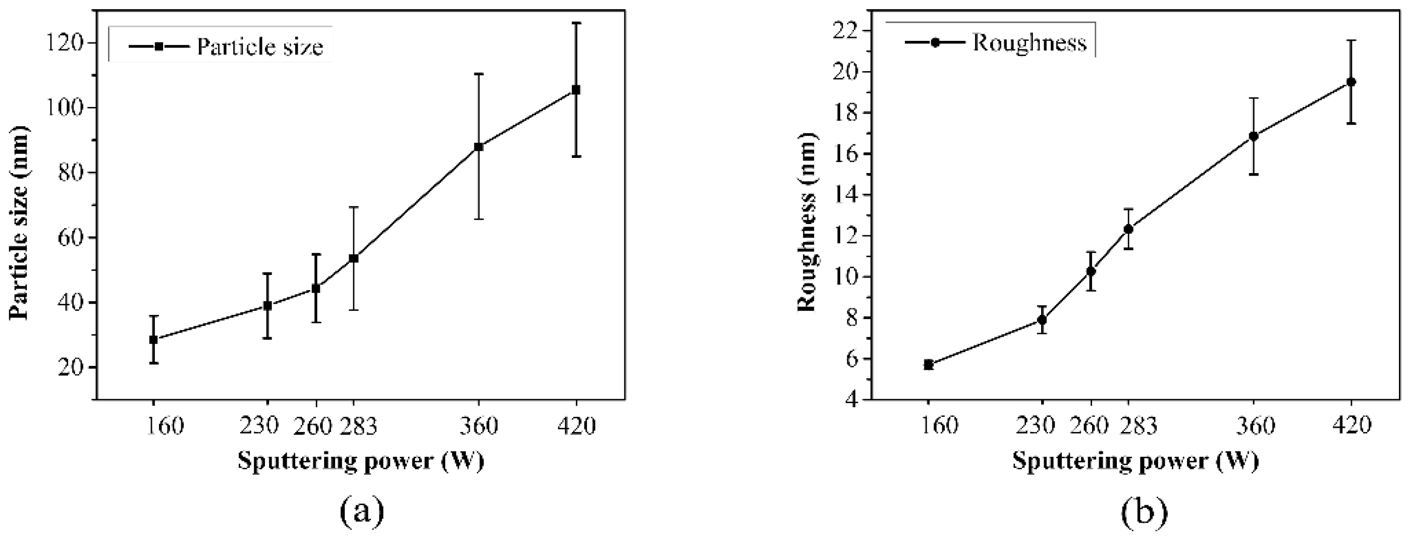
The particle size of Fe films was obtained by means of a particle analysis tool in AFM software, as shown in Figure 6a. As the sputtering power increased, the average particle size became larger. This trend is consistent with previous studies. As mentioned the previous paragraph, the higher the sputtering power, the higher the energy of the incident ions so atoms, clusters or grains are easier to aggregate and grow. Therefore, within a certain range of sputtering power, particle size is proportional to the sputtering power. However, the negative effects of excessive sputtering power cannot be ignored, such as the defects and coarse grains in the films deposited at 360 W; it is the direct reason for the increase of RMS (root mean squared) surface roughness with the increasing sputtering power, as shown in Figure 6b. Combining the AFM results above, the Fe films deposited at 230 W and at 283 W possessed regularly arranged grains, an inhomogeneous particle size distribution and a small surface roughness at the same time. They had formed some coarse grains in the Fe films prepared at 283 W and had larger particle size fluctuations than the Fe films at 230 W, as shown in the section analysis of the films, Figure 5g–l. Therefore, the Fe films at 230 W have the optimal surface structure.
3.4. Magnetic Properties
In our experiments, the magnetic hysteresis loops of iron films deposited at different sputtering powers were measured. We found that the iron film was difficult to be magnetized to saturation perpendicular to the film. Therefore, the in-plate magnetic hysteresis loops were chosen to study how the sputtering power affects the magnetic properties of Fe films deposited with the magnetron sputtering process, as shown in Figure 7a. Figure 7b–d shows the saturation magnetization Ms, coercivity Hc, and squareness ratio Mr/Ms (Mr is the remanence) of the Fe film with different sputtering powers. The detailed magnetic properties of representative samples are shown in Table 1.
In comparing the Ms of the Fe films deposited at different sputtering powers, it was observed that there is no obvious linear relationship between them. Further, the value of Ms increased first and then decreased with the sputtering power, as shown in Figure 7b. The iron film deposited at 230 W had the highest Ms, reaching 92% of the bulk iron [42]. At the same time, Ms also had obvious advantages compared to the films prepared by other preparation methods, as shown in Table 1. The low power resulted in a low density due to the small sputtering yield [27]. By increasing the sputtering power, the Fe films densified, but excessive sputtering power led to coarse grains and uneven distribution, which resulted in high defects [43]. In order to further explain the effect of the sputtering power on Fe films, the particle size (Figure 6a) and size distribution (Figure 5g–l) must be mentioned again. As the sputtering power increased, the average particle size gradually increased. The film prepared at 230 W had the smallest size dispersion, indicating that its structure was the most uniform. Combined with the fine grain size, the Fe film at 230 W exhibited the optimal Ms. Though the thickness of the Fe film increased at a high power, the density of the film decreased due to the uneven distribution of coarse grains and defects. Therefore, the sputtering power greatly affected the saturation magnetization of the film [43].
Figure 7c is the Hc of Fe films with different sputtering powers. The result indicated that the value of Hc increased with the increase in the sputtering power and decreased at 360 W. The internal stress and defect greatly affected the Hc by the pining effect during the magnetization, which restrained the rotation of the magnetic domain. The higher the sputtering power, the higher the energy of the argon ion bombardment on the target, which resulted in a larger content of internal stress and tissue defects during film deposition. Therefore, there was a smaller Hc at 160 W, 230 W and 260 W than there was at 283 W. According to the random anisotropic model, the Fe film at 360 W and 420 W with the large grain size and inhomogeneous size distribution should have a larger Hc than at 283 W, but our result was the opposite. Some studies have proven that an applied magnetic field in the growth process of iron films could effectively improve the disorder structure [6]. At a high sputtering power, the magnetic field from the magnetron sputtering method introduced a noticeable positive effect, leading to the ordering of the film structure and low defects. Further, the Hc of Fe films at 360 W was smaller than it was at 283 W. Therefore, the sputtering power has a significant effect on the Hc of Fe films.
The sputtering power also affects the Mr/Ms of the Fe films. The Fe film deposited at 230 W had a smaller Mr/Ms than at 160 W. This was mainly due to the small grin size and narrow distribution, which led to the large Ms. The appearance of the columnar grain led to larger disorder and crystal anisotropy. Thus, the Mr/Ms of Fe films at 260 W and 283 W increased. The excessive sputtering power enhanced the magnetic field effect, which improved the disordered structure. Therefore, when the sputtering power was further increased, the Mr/Ms started to decrease like the films at 360 W and 420 W.
When we combine all of the above magnetic parameters, we can conclude that the sputtering power has a great influence on the magnetic properties of the Fe films deposited by magnetron sputtering method, especially Ms. In this research, the sputtering power to obtain high saturation magnetization was 230 W.
However, in order to achieve excellent magnetic properties, we need to consider the effects of multiple sputtering parameters (vacuum, working pressure, deposition time, substrate temperature, etc.). Therefore, subsequent systematic research on the influence of other sputtering parameters on the structure and magnetic properties of iron thin film is also necessary.
4. Discussion
In this article, we successfully deposited hundreds of nanometers of iron film by RF magnetron sputtering mainly to study the effect of the sputtering power on the structure, morphology and soft magnetic properties of Fe film. The XRD structure showed that all Fe films have a polycrystalline bcc structure and (110) preferred orientation. According to the Bragg equation calculation, the larger the sputtering power, the larger the average grain size, which is consistent with the results of AFM particle size analysis. The main reason is that the sputtering power will affect the grain growth mode. As the sputtering power increases, it gradually changes from a small island-like growth to a thick columnar growth. However, from the surface morphology and height profile, we saw that the iron film deposited under 230 W had the most uniform grain size distribution, and the grain size was relatively small. The VSM results showed that the iron film prepared under 230 W had good comprehensive properties (highest Ms, lower coercivity and squareness ratio). Therefore, the sputtering power plays a vital role in structure and magnetic properties.
Author Contributions
All authors have read and agreed to the published version of the manuscript. Conceptualization, B.Y.; methodology, T.L.; validation, C.Z. and T.L.; formal analysis, C.Z., B.Y. and X.W.; investigation, C.Z.; data curation, C.Z.; writing—original draft preparation, C.Z.; writing—review and editing, X.W.; project administration, B.Y.; funding acquisition, B.Y.
Funding
This work was supported by the National Thirteenth Five-Year Plan for National Key R&D Program: Research on Simulation Verification and Design Optimization of Key Technologies for High Speed Maglev Transportation System. The project number is: 2016YFB1200602-02.
Conflicts of Interest
The authors declare no conflicts of interest.
References
- Brajpuriya, R.; Tripathi, S.; Sharma, A.; Shripathi, T.; Chaudhari, S.M. Thickness dependent structural and magnetic properties of ultra-thin Fe/Al structures. Eur. Phys. J. B 2006, 51, 131–136. [Google Scholar] [CrossRef]
- Du, J.; Li, G.; Liu, S.; Liu, T.; Wu, C.; Wang, Q. Enhancement of magnetic properties by adjusted structure in Fe nanocrystalline films via annealing and applying high magnetic field at different film-formation stages. J. Magn. Magn. Mater. 2020, 495, 165857. [Google Scholar] [CrossRef]
- Feng, C.; Yin, J.; Niu, J.-G.; Zhang, Q.; Gu, L.; Yang, F.; Tang, X.; Xu, L.; Gong, K.; Cao, Y.; et al. Construction of FeN alloy films with ultra-strong magnetism and tunable magnetic anisotropy for spintronic application. J. Alloys Compd. 2017, 725, 32–40. [Google Scholar] [CrossRef]
- Zaman, S.S.; Dvořák, P.; Ritter, R.; Buchsbaum, A.; Stickler, D.; Oepen, H.P.; Schmid, M.; Varga, P. In-situ magnetic nano-patterning of Fe films grown on Cu(100). J. Appl. Phys. 2011, 110, 024309. [Google Scholar] [CrossRef] [Green Version]
- Muraca, D.; Cremaschi, V.; Moya, J.; Sirkin, H. FINEMET type alloy without Si: Structural and magnetic properties. J. Magn. Magn. Mater. 2008, 320, 1639–1644. [Google Scholar] [CrossRef]
- Liu, S.; Ma, Y.; Chang, L.; Li, G.; Wang, J.; Wang, Q. Effect of doping SiO2 and applying high magnetic field during the film growth on structure and magnetic properties of evaporated Fe films. Thin Solid Films 2018, 651, 1–6. [Google Scholar] [CrossRef]
- Du, J.; Li, G.; Wang, Q.; Ma, Y.; Cao, Y.; He, J. Microstructural evolution and magnetic properties of nanocrystalline Fe films prepared in a high magnetic field. Vacuum 2015, 121, 88–95. [Google Scholar] [CrossRef]
- Park, S.J.; Liu, C.-H.; Kim, H.S.; Park, N.J.; Jin, S.; Han, J.H. Texture and magnetic properties of Fe thin films fabricated by field-sputtering vs field-annealing. Thin Solid Films 2015, 594, 178–183. [Google Scholar] [CrossRef]
- Fan, J.; Sun, J.; Yang, Y.; Liang, R.; Jiang, Y.; Zhang, J.; Xu, X. Effect of nitrogen and cobalt additions on surface morphology and magnetic properties of Fe thin films. J. Alloys Compd. 2016, 662, 541–545. [Google Scholar] [CrossRef]
- Ahmad, S.S.; He, W.; Zhang, Y.-S.; Tang, J.; Li, Y.; Gul, Q.; Zhang, X.-Q.; Cheng, Z.-H. Effect of Ar+ beam sputtering on the magnetic anisotropy of Fe thin films deposited on the MgO(0 0 1) substrate. Results. Phys. 2017, 7, 1531–1535. [Google Scholar] [CrossRef]
- Papamihail, K.; Mergia, K.; Ott, F.; Serruys, Y.; Speliotis, T.; Apostolopoulos, G.; Messoloras, S. Fe+ ion irradiation induced changes in structural and magnetic properties of iron films. Nucl. Mater. Energy 2016, 9, 459–464. [Google Scholar] [CrossRef] [Green Version]
- He, S.H.; Zha, C.L.; Ma, B.; Zhang, Z.Z.; Jin, Q.Y. Formation of (002) texture in Fe films prepared by thermal treatment. J. Magn. Magn. Mater. 2007, 310, 2656–2658. [Google Scholar] [CrossRef]
- Sandu, S.G.; Palade, P.; Schinteie, G.; Birsan, A.; Trupina, L.; Kuncser, V. Tuning structural and magnetic properties of Fe films on Si substrates by hydrogenation processing. Mater. Sci. Eng. B 2014, 181, 24–32. [Google Scholar] [CrossRef]
- Serizawa, K.; Ohtake, M.; Kawai, T.; Futamoto, M.; Kirino, F.; Inaba, N. Influence of crystal orientation on the magnetostriction behavior of Fe films formed on MgO single-crystal substrates. J. Magn. Magn. Mater. 2019, 477, 420–426. [Google Scholar] [CrossRef]
- Gao, C.; Brandt, O.; Lähnemann, J.; Herfort, J.; Schönherr, H.-P.; Jahn, U.; Jenichen, B. Effect of growth temperature on the structural, morphological and magnetic properties of Fe films on GaN(0001). J. Cryst. Growth 2011, 323, 359–362. [Google Scholar] [CrossRef]
- Zhang, Y.-S.; He, W.; Ye, J.; Hu, B.; Tang, J.; Zhang, X.-Q.; Cheng, Z.-H. Temperature dependence of magnetic anisotropies in ultrathin Fe film on vicinal Si(111). Phys. B Condens. Matter 2017, 512, 32–38. [Google Scholar] [CrossRef]
- Javed, A.; Morley, N.A.; Gibbs, M.R.J. Effect of growth parameters on the structure and magnetic properties of thin polycrystalline Fe films fabricated on Si<100> substrates. Appl. Surf. Sci. 2011, 257, 5586–5590. [Google Scholar] [CrossRef]
- Getman, A.; Sivov, A.; Perov, N.S.; Iakubov, I.T.; Rozanov, K.N.; Ryzhikov, I.A.; Starostenko, S.N. Static and dynamic magnetic properties of Fe films. J. Magn. Magn. Mater. 2004, 272–276, E909–E910. [Google Scholar] [CrossRef]
- Bensehil, I.; Kharmouche, A.; Bourzami, A. Synthesis, Structural, and Magnetic Properties of Fe Thin Films. J. Supercond. Nov. Magn. 2016, 30, 795–799. [Google Scholar] [CrossRef]
- Sharma, A.; Tripathi, J.; Tripathi, S.; Ugochukwu, K.C. Investigation of magnetic and structural properties of Au capped Fe thin films. Phys. B Condens. Matter 2019, 560, 81–84. [Google Scholar] [CrossRef]
- Balashev, V.V.; Ermakov, K.S.; Chebotkevich, L.A.; Korobtsov, V.V. Electrical and Magnetic Properties of Ultrathin Polycrystalline Fe Films Grown on SiO2/Si(001). Tech. Phys. Lett. 2018, 44, 595–598. [Google Scholar] [CrossRef]
- Niu, Y.R.; Man, K.L.; Pavlovska, A.; Bauer, E.; Altman, M.S. Fe on W(001) from continuous films to nanoparticles: Growth and magnetic domain structure. Phy. Rev. B 2017, 95. [Google Scholar] [CrossRef] [Green Version]
- Gouralnik, A.S.; Galkin, N.G.; Ivanov, V.A.; Cherednichenko, A.I.; Plotnikov, V.S.; Pustovalov, E.V. Effect of deposition rate and a-Si precursor or cap layer on structure and magnetic properties of iron films on silicon substrates. Thin Solid Films 2011, 519, 8520–8523. [Google Scholar] [CrossRef]
- Kim, T.C.; Lee, S.H.; Jung, H.K.; Kim, Y.E.; Choi, J.W.; Yang, D.; Kim, D.H. Effect of sputtering conditions on the structure and magnetic properties of self-assembled BiFeO3-CoFe2O4 nanocomposite thin films. J. Magn. Magn. Mater. 2019, 471, 116–123. [Google Scholar] [CrossRef]
- Saravanan, L.; Raja, M.M.; Prabhu, D.; Therese, H.A. Influence of sputtering power on structural and magnetic properties of as-deposited, annealed and ERTA Co2FeSi films: A comparative study. Phys. B Condens. Matter 2018, 531, 180–184. [Google Scholar] [CrossRef]
- Wang, K.; Huang, Y.; Xu, Z.; Dong, S.; Chen, R. Effect of sputtering power on the magnetic properties of amorphous perpendicular TbFeCo films. J. Magn. Magn. Mater. 2017, 424, 89–92. [Google Scholar] [CrossRef]
- Basumatary, H.; Arout Chelvane, J.; Sridhara Rao, D.V.; Kamat, S.V.; Ranjan, R. Effect of sputtering parameters on the structure, microstructure and magnetic properties of Tb-Fe films. Thin Solid Films 2015, 583, 1–6. [Google Scholar] [CrossRef]
- Srinivas, K.; Manivel Raja, M.; Sridhara Rao, D.V.; Kamat, S.V. Effect of sputtering pressure and power on composition, surface roughness, microstructure and magnetic properties of as-deposited Co2FeSi thin films. Thin Solid Films 2014, 558, 349–355. [Google Scholar] [CrossRef]
- Chen, G.-J.; Jian, S.-R.; Jang, J.S.-C.; Shih, Y.-H.; Chen, Y.-T.; Jen, S.-U.; Juang, J.-Y. The effects of annealing temperature and sputtering power on the structure and magnetic properties of the Co-Fe-Zr-B thin films. Intermetallics 2012, 30, 127–131. [Google Scholar] [CrossRef]
- Meng, X.; Du, Y.; Gao, X. Face–centered cubic p–type NiO films room–temperature prepared via direct-current reactive magnetron sputtering–Influence of sputtering power on microstructure, optical and electrical behaviors. Phys. B Condens. Matter 2020, 579, 411897. [Google Scholar] [CrossRef]
- Lee, M.; Park, Y.; Kim, K.; Hong, J. Influence of sputtering conditions on the properties of aluminum-doped zinc oxide thin film fabricated using a facing target sputtering system. Thin Solid Films 2020, 703, 137980. [Google Scholar] [CrossRef]
- Simanjuntak, F.M.; Ohno, T.; Samukawa, S. Influence of rf sputter power on ZnO film characteristics for transparent memristor devices. AIP Adv. 2019, 9, 105216. [Google Scholar] [CrossRef] [Green Version]
- Ferdaous, M.T.; Shahahmadi, S.A.; Sapeli, M.M.I.; Chelvanathan, P.; Akhtaruzzaman, M.; Tiong, S.K.; Amin, N. Interplay between variable direct current sputtering deposition process parameters and properties of ZnO:Ga thin films. Thin Solid Films 2018, 660, 538–545. [Google Scholar] [CrossRef]
- Sakthivel, P.; Murugan, R.; Asaithambi, S.; Karuppaiah, M.; Vijayaprasath, G.; Rajendran, S.; Hayakawa, Y.; Ravi, G. Radio frequency power induced changes of structural, morphological, optical and electrical properties of sputtered cadmium oxide thin films. Thin Solid Films 2018, 654, 85–92. [Google Scholar] [CrossRef]
- Azevedo Neto, N.F.; Leite, D.M.G.; Lisboa-Filho, P.N.; da Silva, J.H.D. Role of the reactive sputtering deposition power in the phase control of cobalt oxide films. J. Vac. Sci. Technol. A 2018, 36, 061512. [Google Scholar] [CrossRef]
- Chelvanathan, P.; Shahahmadi, S.A.; Arith, F.; Sobayel, K.; Aktharuzzaman, M.; Sopian, K.; Alharbi, F.H.; Tabet, N.; Amin, N. Effects of RF magnetron sputtering deposition process parameters on the properties of molybdenum thin films. Thin Solid Films 2017, 638, 213–219. [Google Scholar] [CrossRef]
- Jen, S.U.; Tsai, T.L. Optimization of sputter deposition parameters for magnetostrictive Fe62Co19Ga19/Si(100) films. J. Appl. Phys. 2012, 111, 07A939. [Google Scholar] [CrossRef]
- Atkins, E. Elements of X-ray Diffraction. Phys. Today 1978, 10, 50. [Google Scholar] [CrossRef]
- Jhanwar, P.; Kumar, A.; Verma, S.; Rangra, K.J. Effect of Sputtering Power on the Growth of Ru films Deposited by Magnetron Sputtering. AIP Conf. Proc. 2016, 020073, 1–5. [Google Scholar] [CrossRef]
- De, R.; Haque, S.M.; Tripathi, S.; Prathap, C.; Rao, K.D.; Sahoo, N.K. Effect of sputtering power on MgF2 thin films deposited by sputtering technique under fluorine trapping. AIP Conf. Proc. 2016, 080078, 1–3. [Google Scholar] [CrossRef]
- Xiao, W.; Deng, H.; Zou, S.; Ren, Y.; Tang, D.; Lei, M.; Xiao, C.; Zhou, X.; Chen, Y. Effect of roughness of substrate and sputtering power on the properties of TiN coatings deposited by magnetron sputtering for ATF. J. Nucl. Mater. 2018, 509, 542–549. [Google Scholar] [CrossRef]
- Gao, C.; Brandt, O.; Schönherr, H.-P.; Jahn, U.; Herfort, J.; Jenichen, B. Thermal stability of epitaxial Fe films on GaN(0001). Appl. Phys. Lett. 2009, 111906, 1–3. [Google Scholar] [CrossRef] [Green Version]
- Kodam, U.; K.B., A.B.; Markandeyulu, G. In house designed magnetron sputtering source: Effect of power and annealing on structural, optical and magnetic properties of NiFe2−xLuxO4 (x = 0, 0.075) thin films. Thin Solid Films 2018, 662, 180–186. [Google Scholar] [CrossRef]
Figure 1.
XRD patterns of Fe films prepared at different sputtering powers: (a) 160 W, (b) 230 W, (c) 260 W, (d) 283 W, (e) 360 W, and (f) 420 W.
Figure 1.
XRD patterns of Fe films prepared at different sputtering powers: (a) 160 W, (b) 230 W, (c) 260 W, (d) 283 W, (e) 360 W, and (f) 420 W.

Figure 2.
The relationship between the average grain size of the Fe film and the sputtering power.

Figure 3.
Cross-sectional SEM views of the Fe films fabricated at different sputtering powers: (a) 160 W, (b) 230 W, (c) 260 W, (d) 283 W, (e) 360 W, and (f) 420 W.
Figure 3.
Cross-sectional SEM views of the Fe films fabricated at different sputtering powers: (a) 160 W, (b) 230 W, (c) 260 W, (d) 283 W, (e) 360 W, and (f) 420 W.

Figure 4.
Line charts of the thickness of Fe films as a function of the sputtering power.

Figure 5.
AFM micrographs of Fe films with different sputtering powers: (a) 160 W, (b) 230 W, (c) 260 W, (d) 283 W, (e) 360 W, (f) 420 W; respective sectional height contour: (g) 160 W, (h) 230 W, (i) 260 W, (j) 283 W, (k) 360 W, (l) 420 W.
Figure 5.
AFM micrographs of Fe films with different sputtering powers: (a) 160 W, (b) 230 W, (c) 260 W, (d) 283 W, (e) 360 W, (f) 420 W; respective sectional height contour: (g) 160 W, (h) 230 W, (i) 260 W, (j) 283 W, (k) 360 W, (l) 420 W.

Figure 6.
The particle size (a) and RMS of surface roughness (b) of iron films at different sputtering powers.
Figure 6.
The particle size (a) and RMS of surface roughness (b) of iron films at different sputtering powers.

Figure 7.
Magnetic hysteresis loops of Fe films at different sputtering powers (a); saturation magnetization (Ms) (b), coercivity (Hc) (c), and squareness ratio Mr/Ms (d) of Fe films prepared at different sputtering powers.
Figure 7.
Magnetic hysteresis loops of Fe films at different sputtering powers (a); saturation magnetization (Ms) (b), coercivity (Hc) (c), and squareness ratio Mr/Ms (d) of Fe films prepared at different sputtering powers.


Table 1.
Magnetic properties of iron thin films under different preparation conditions.
| Samples | Methods | Ms (emu/cm3) | Hc (Oe) | Mr/Ms | References |
|---|---|---|---|---|---|
| 160 W | RF magnetron sputtering | 1157 | 90 | 0.437 | This research |
| 230 W | 1566 | 112 | 0.401 | ||
| 260 W | 1477 | 119 | 0.417 | ||
| 283 W | 1418 | 142 | 0.446 | ||
| 360 W | 1350 | 108 | 0.376 | ||
| 420 W | 1268 | 104 | 0.363 | ||
| RT 0 T | Thermal evaporation | 1213 | 58 | - | Ref [7] |
| 0 T | Molecular beam vapor deposition | 1491 | - | 0.54 | Ref [2] |
© 2020 by the authors. Licensee MDPI, Basel, Switzerland. This article is an open access article distributed under the terms and conditions of the Creative Commons Attribution (CC BY) license (http://creativecommons.org/licenses/by/4.0/).
Share and Cite
MDPI and ACS Style
Zhou, C.; Li, T.; Wei, X.; Yan, B. Effect of the Sputtering Power on the Structure, Morphology and Magnetic Properties of Fe Films. Metals 2020, 10, 896. https://doi.org/10.3390/met10070896
AMA Style
Zhou C, Li T, Wei X, Yan B. Effect of the Sputtering Power on the Structure, Morphology and Magnetic Properties of Fe Films. Metals. 2020; 10(7):896. https://doi.org/10.3390/met10070896
Chicago/Turabian StyleZhou, Chunxia, Tongkui Li, Xianshun Wei, and Biao Yan. 2020. "Effect of the Sputtering Power on the Structure, Morphology and Magnetic Properties of Fe Films" Metals 10, no. 7: 896. https://doi.org/10.3390/met10070896
Note that from the first issue of 2016, this journal uses article numbers instead of page numbers. See further details here.