High-Identical Numerical Aperture, Multifocal Microlens Array through Single-Step Multi-Sized Hole Patterning Photolithography


Abstract
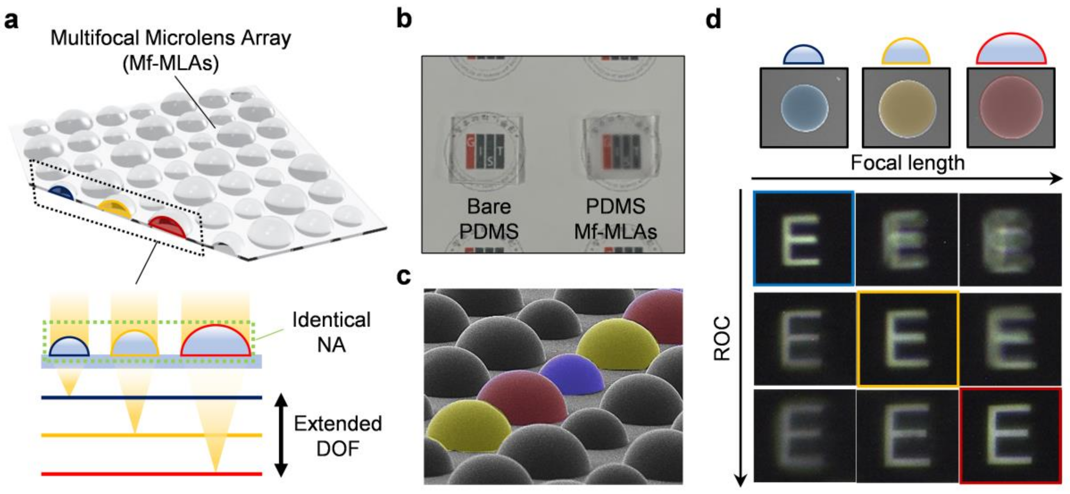
:1. Introduction
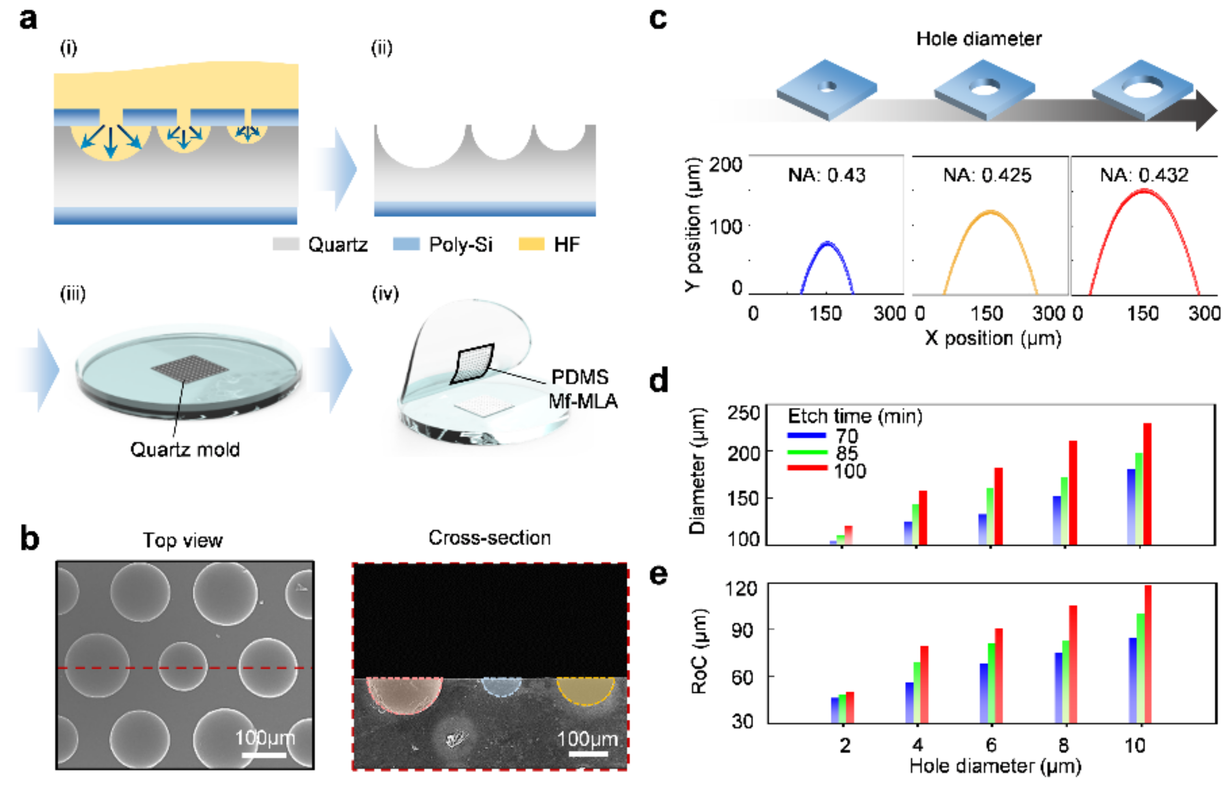
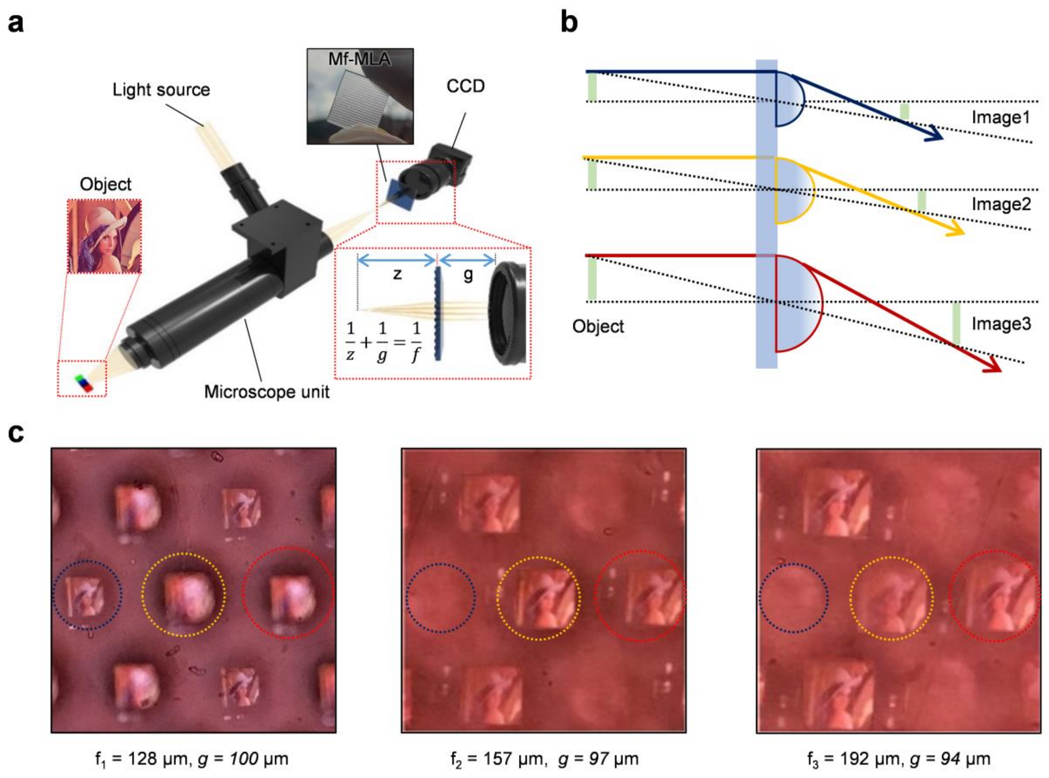
2. Materials and Methods
Design and Fabrication of Mf-MLA
3. Results and Discussion
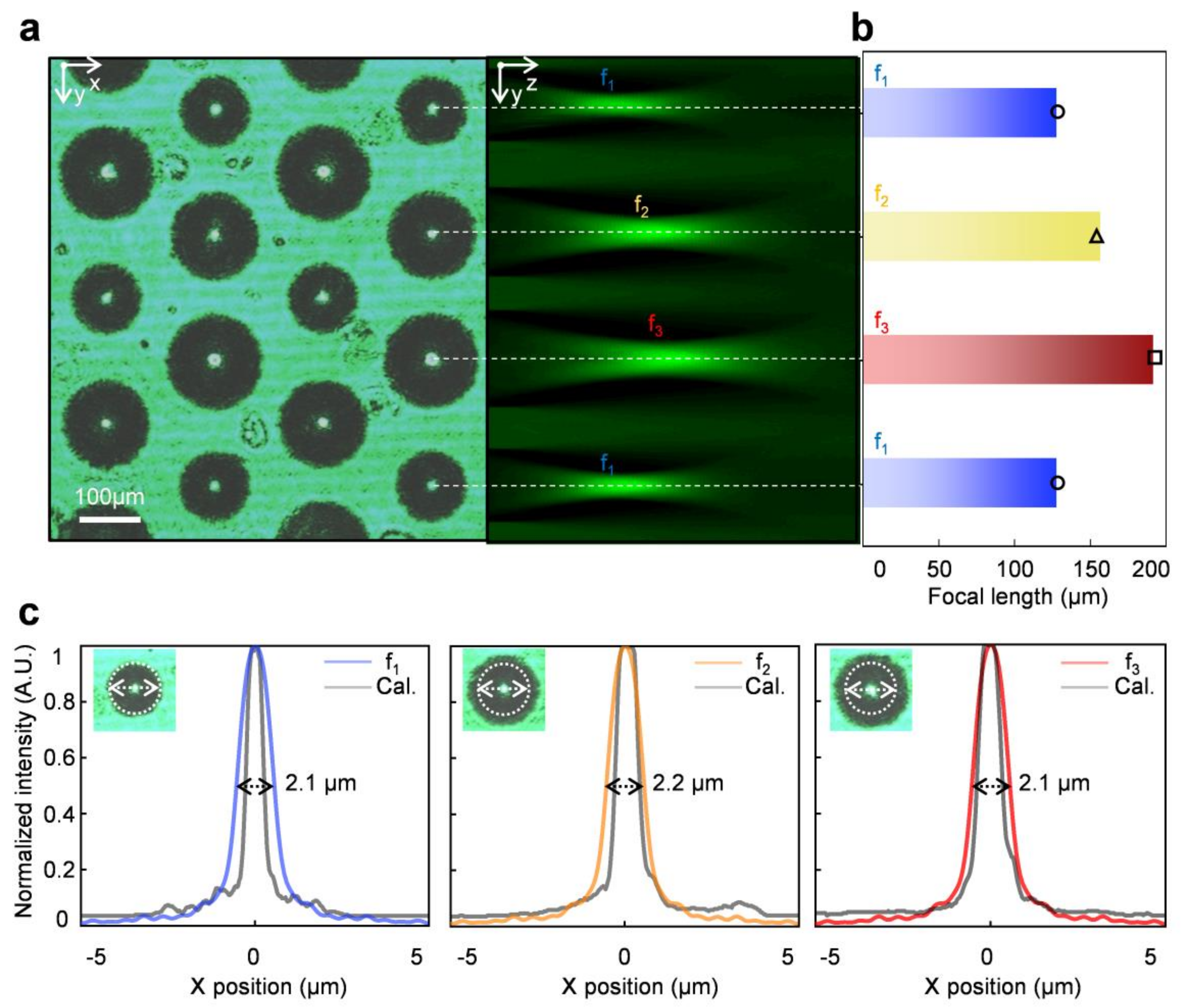
3.1. Characterization of Mf-MLA
3.2. Multifocal Arrayed Images
4. Conclusions
Author Contributions
Funding
Conflicts of Interest
References
- Song, Y.M.; Xie, Y.; Malyarchuk, V.; Xiao, J.; Jung, I.; Choi, K.J.; Liu, Z.; Park, H.; Lu, C.; Kim, R.H.; et al. Digital cameras with designs inspired by the arthropod eye. Nature 2013, 497, 95–99. [Google Scholar] [CrossRef] [PubMed]
- Keum, D.; Jang, K.W.; Jeon, D.S.; Hwang, C.S.H.; Buschbeck, E.K.; Kim, M.H.; Jeong, K.H. Xenos peckii vision inspires an ultrathin digital camera. Light Sci. Appl. 2018, 7, 80. [Google Scholar] [CrossRef] [PubMed] [Green Version]
- Lee, G.J.; Choi, C.; Kim, D.; Song, Y.M. Bioinspired artificial eyes: Optic components, digital cameras, and visual prostheses. Adv. Funct. Mater 2018, 28, 1705202. [Google Scholar] [CrossRef]
- Lee, W.; Jang, H.; Park, S.; Song, Y.M.; Lee, H. COMPU-EYE: A high resolution computational compound eye. Opt. Express 2016, 24, 2013–2026. [Google Scholar] [CrossRef] [PubMed]
- Endo, Y.; Wakunami, K.; Shimobaba, T.; Kakue, T.; Arai, D.; Ichihashi, Y.; Yamamoto, K.; Ito, T. Computer-generated hologram calculation for real scenes using a commercial portable plenoptic camera. Opt. Commun. 2015, 356, 468–471. [Google Scholar] [CrossRef]
- Sun, J.; Xu, C.; Zhang, B.; Hossain, M.M.; Wang, S.; Qi, H.; Tan, H. Three-dimensional temperature field measurement of flame using a single light field camera. Opt. Express 2016, 24, 1118–1132. [Google Scholar] [CrossRef] [Green Version]
- Apelt, F.; Breuer, D.; Nikoloski, Z.; Stitt, M.; Kragler, F. Phytotyping4D: A light-field imaging system for non-invasive and accurate monitoring of spatio-temporal plant growth. Plant J. 2015, 82, 693–706. [Google Scholar] [CrossRef]
- Uchida, N.; Shibahara, T.; Aoki, T.; Nakajima, H.; Kobayashi, K. 3D face recognition using passive stereo vision. In Proceedings of the IEEE International Conference on Image Processing 2005, Genova, Italy, 14 September 2005; pp. II–950. [Google Scholar]
- Liu, J.; Claus, D.; Xu, T.; Keßner, T.; Herkommer, A.; Osten, W. Light field endoscopy and its parametric description. Opt. Lett. 2017, 42, 1804–1807. [Google Scholar] [CrossRef]
- Geng, J.; Xie, J. Review of 3-D Endoscopic Surface Imaging Techniques. IEEE Sens. J. 2014, 14, 945–960. [Google Scholar] [CrossRef]
- Kim, H.M.; Kim, M.S.; Lee, G.J.; Jang, H.J.; Song, Y.M. Miniaturized 3D Depth Sensing-Based Smartphone Light Field Camera. Sensors 2020, 20, 2129. [Google Scholar] [CrossRef] [Green Version]
- Georgeiv, T.; Intwala, C. Light Field Camera Design for Integral View Photography. In Adobe Technical Report; Adobe Systems Incorporated: San Jose, CA, USA, 2006. [Google Scholar]
- Chang, J.; Kauvar, I.; Hu, X.; Wetzstein, G. Variable Aperture Light Field Photography: Overcoming the Diffraction-Limited Spatio-Angular Resolution Tradeoff. In Proceedings of the 2016 IEEE Conference on Computer Vision and Pattern Recognition (CVPR), Las Vegas, NV, USA, 27–30 June 2016; pp. 3737–3745. [Google Scholar]
- Kim, H.M.; Kim, M.S.; Lee, G.J.; Yoo, Y.J.; Song, Y.M. Large area fabrication of engineered microlens array with low sag height for light-field imaging. Opt. Express 2019, 27, 4435–4444. [Google Scholar] [CrossRef] [PubMed]
- Chen, M.; He, W.; Wei, D.; Hu, C.; Shi, J.; Zhang, X.; Wang, H.; Xie, C. Depth-of-Field-Extended Plenoptic Camera Based on Tunable Multi-Focus Liquid-Crystal Microlens Array. Sensors 2020, 20, 4142. [Google Scholar] [CrossRef] [PubMed]
- Georgiev, T.; Lumsdaine, A. The multifocus plenoptic camera. In Digital Photography, VIII; Battiato, S., Rodricks, B.G., Sampat, N., Imai, F.H., Xiao, F., Eds.; International Society for Optics and Photonics SPIE: Bellingham, WA, USA, 2012; Volume 8299, p. 829908. [Google Scholar]
- Di, S.; Lin, H.; Du, R. An artificial compound eyes imaging system based on MEMS technology. In Proceedings of the 2009 IEEE International Conference on Robotics and Biomimetics (ROBIO), Guilin, China, 19–23 December 2009; pp. 13–18. [Google Scholar]
- Albero, J.; Nieradko, L.; Gorecki, C.; Ottevaere, H.; Gomez, V.; Thienpont, H.; Pietarinen, J.; Päivänranta, B.; Passilly, N. Fabrication of spherical microlenses by a combination of isotropic wet etching of silicon and molding techniques. Opt. Express 2009, 17, 6283–6292. [Google Scholar] [CrossRef]
- Hu, Y.; Chen, Y.; Ma, J.; Li, J.; Huang, W.; Chu, J. High-efficiency fabrication of aspheric microlens arrays by holographic femtosecond laser-induced photopolymerization. Appl. Phys. Lett. 2013, 103, 141112. [Google Scholar] [CrossRef]
- Huang, J.Y.; Lu, Y.S.; Yeh, J.A. Self-assembled high NA microlens arrays using global dielectricphoretic energy wells. Opt. Express 2006, 14, 10779–10784. [Google Scholar] [CrossRef]
- Ko, D.H.; Tumbleston, J.R.; Henderson, K.J.; Euliss, L.E.; DeSimone, J.M.; Lopez, R.; Samulski, E.T. Biomimetic microlens array with antireflective “moth-eye” surface. Soft Matter 2011, 7, 6404–6407. [Google Scholar] [CrossRef]
- Jang, H.J.; Kim, Y.J.; Yoo, Y.J.; Lee, G.J.; Kim, M.S.; Chang, K.S.; Song, Y.M. Double-sided anti-reflection nanostructures on optical convex lenses for imaging applications. Coatings 2019, 9, 404. [Google Scholar] [CrossRef] [Green Version]
- Park, M.K.; Lee, H.J.; Park, J.S.; Bae, J.M.; Kim, H.R. Design and Fabrication of Multi-Focusing Microlens Array with Different Numerical Apertures by using Thermal Reflow Method. J. Opt. Soc. Korea 2014, 18, 71–77. [Google Scholar] [CrossRef] [Green Version]
- Bae, S.I.; Kim, K.; Yang, S.; won Jang, K.; Jeong, K.H. Multifocal microlens arrays using multilayer photolithography. Opt. Express 2020, 28, 9082–9088. [Google Scholar] [CrossRef]
- Shiroma, L.S.; Piazzetta, M.H.O.; Duarte-Junior, G.F.; Coltro, W.K.T.; Carrilho, E.; Gobbi, A.L.; Lima, R.S. Self-regenerating and hybrid irreversible/reversible PDMS microfluidic devices. Sci. Rep. 2016, 6, 26032. [Google Scholar] [CrossRef] [PubMed]
- Li, T.J.; Li, S.; Yuan, Y.; Liu, Y.D.; Xu, C.L.; Shuai, Y.; Tan, H.P. Multi-focused microlens array optimization and light field imaging study based on Monte Carlo method. Opt. Express 2017, 25, 8274–8287. [Google Scholar] [CrossRef] [PubMed]
- Chen, Y.; Xiong, B.; Xue, Y.; Jin, X.; Greene, J.; Tian, L. Design of a high-resolution light field miniscope for volumetric imaging in scattering tissue. Biomed. Opt. Express 2020, 11, 1662–1678. [Google Scholar] [CrossRef] [PubMed]


| Hole Size | 2 μm | 6 μm | 10 μm |
|---|---|---|---|
| Roughness (Ra) | 0.044 μm | 0.036 μm | 0.034 μm |
Publisher’s Note: MDPI stays neutral with regard to jurisdictional claims in published maps and institutional affiliations. |
© 2020 by the authors. Licensee MDPI, Basel, Switzerland. This article is an open access article distributed under the terms and conditions of the Creative Commons Attribution (CC BY) license (http://creativecommons.org/licenses/by/4.0/).
Share and Cite
Lee, J.H.; Chang, S.; Kim, M.S.; Kim, Y.J.; Kim, H.M.; Song, Y.M. High-Identical Numerical Aperture, Multifocal Microlens Array through Single-Step Multi-Sized Hole Patterning Photolithography. Micromachines 2020, 11, 1068. https://doi.org/10.3390/mi11121068
Lee JH, Chang S, Kim MS, Kim YJ, Kim HM, Song YM. High-Identical Numerical Aperture, Multifocal Microlens Array through Single-Step Multi-Sized Hole Patterning Photolithography. Micromachines. 2020; 11(12):1068. https://doi.org/10.3390/mi11121068
Chicago/Turabian StyleLee, Joong Hoon, Sehui Chang, Min Seok Kim, Yeong Jae Kim, Hyun Myung Kim, and Young Min Song. 2020. "High-Identical Numerical Aperture, Multifocal Microlens Array through Single-Step Multi-Sized Hole Patterning Photolithography" Micromachines 11, no. 12: 1068. https://doi.org/10.3390/mi11121068