Environmental Effects on the Electrical Characteristics of Back-Gated WSe2 Field-Effect Transistors
by
 , ,
, ,
Francesca Urban
1,2 ,
,
Nadia Martucciello
2,
Lisanne Peters
3,
Niall McEvoy
3 and
Antonio Di Bartolomeo
1,2,*
1
Physics Department “E. R. Caianiello” and Interdepartmental Centre NanoMates, University of Salerno, via Giovanni Paolo II n. 132, 84084 Fisciano, Italy
2
CNR-SPIN Salerno, via Giovanni Paolo II n. 132, 84084 Fisciano, Italy
3
AMBER & School of Chemistry, Trinity College Dublin, 2 Dublin, Ireland
*
Author to whom correspondence should be addressed.
Nanomaterials 2018, 8(11), 901; https://doi.org/10.3390/nano8110901
Submission received: 4 October 2018
/
Revised: 31 October 2018
/
Accepted: 1 November 2018
/
Published: 3 November 2018
(This article belongs to the Special Issue 2D Materials and Van der Waals Heterostructures: Physics and Applications)
Abstract
:We study the effect of polymer coating, pressure, temperature, and light on the electrical characteristics of monolayer back-gated transistors with contacts. Our investigation shows that the removal of a layer of poly(methyl methacrylate) (PMMA) or a decrease of the pressure change the device conductivity from p- to n-type. From the temperature behavior of the transistor transfer characteristics, a gate-tunable Schottky barrier at the contacts is demonstrated and a barrier height of 70 meV in the flat-band condition is measured. We also report and discuss a temperature-driven change in the mobility and the subthreshold swing that is used to estimate the trap density at the interface. Finally, from studying the spectral photoresponse of the , it is proven that the device can be used as a photodetector with a responsivity of at and optical power.
1. Introduction
The continuous downscaling of the channel length and thickness in modern field effect transistors (FETs) has increased the need for atomically-layered materials to minimize short channel effects at extreme scaling limits [1,2]. Layered transition metal dichalcogenides (TMDs), owing to their two-dimensional structure, reasonable charge-carrier mobilities, and the absence of dangling bonds can enable extreme channel length scaling and have recently emerged as promising materials for future electronic and optoelectronic devices [3,4,5,6,7]. These graphene-like materials offer the advantages of sizeable and non-zero bandgap, high on/off ratio and quasi-ideal subthreshold swing, mechanical flexibility, and thermal and chemical stability. Similar to graphene, their electronic transport properties are strongly influenced by the choice of the metal contacts [8,9,10], by interface traps and impurities [11,12], as well as by structural defects and environmental exposure [13,14,15,16,17]. These effects need to be understood and controlled for technological applications.
Molybdenum disulfide () has been one of the most heavily investigated systems from the TMD family to date [18,19,20,21,22,23,24,25]. Similar to , tungsten diselenide (, whose electrical and optical properties have been relatively less explored [26], is characterized by an indirect bandgap (1.0–1.2 eV) in the bulk form and shows a transition to a direct gap of 1.6 eV when it is thinned to monolayer [27]. Recent reports on FETs have demonstrated a relatively high field-effect mobility controllable by temperature and bias voltage [26,28], an ideal subthreshold swing [29] and an on/off ratio up to . The ambipolar behavior, controllable using different metal contacts, like In or Pd [8], which favor electron and hole injection, respectively [26,30,31], makes mono- and few-layer an interesting material for complementary logic applications; indeed, a stable -based CMOS technology has been demonstrated [32,33,34].
A great challenge for electronic integration of is the development of low-resistance ohmic contacts, a task often complicated by the appearance of Schottky barriers due to the occurrence of Fermi level pinning [35,36]. Accordingly, several studies have aimed to clarify the role of the contacts, focusing on the carrier transport at the /metal interface [30,37,38].
In this paper, we study back-gated monolayer devices with Ni contacts, measuring their electrical characteristics under different conditions, considering, for instance, the effect of a poly(methyl methacrylate) (PMMA) coating layer, and the dependence on the chamber pressure and the sample temperature. Similar to graphene [39,40], we observe that PMMA strongly influences the electrical transport, in this case to the extent that the polarity of the device changes from p-type to n-type conduction when the PMMA layer is removed. We demonstrate that lowering the pressure on air-exposed FETs affects their characteristics in a similar way to PMMA, turning the conduction from p- to n-type. Furthermore, from the current-voltage (I-V) characteristics measured at different temperatures, we prove a gate modulation of the Schottky barrier (SB) at the contacts.
In addition, we study the temperature dependence of the carrier mobility and the subthreshold swing and show that both undergo a change of behavior with increasing temperature. From the subthreshold swing data, we derive the interface trap density, which affects the photoresponse of the device. The monolayer device, characterized at several laser wavelengths, achieves a responsivity as high as at 700 nm, i.e. at a photon energy close to the bandgap.
2. Experimental
The flakes were grown in a two-zone heating furnace. Selenium pellets (Sigma-Aldrich Inc, St. Louis, MO, USA) were evaporated at 250 °C in the lower-temperature, upstream heating zone, while in the high-temperature, downstream zone the tungsten precursor (20 nm sputtered and subsequently oxidized tungsten) was placed with the growth substrate. A highly p-doped Si (silicon) substrate covered by 300 nm of (silicon dioxide) was placed top down on the tungsten precursor, which was heated up to 850 °C. The tungsten precursor/growth substrate stack forms a microreactor, which increases the reactivity due to the close proximity between the precursor and growth substrate, requiring a lower amount of precursor and minimizing the contamination of the furnace. This is a similar approach to previous reports on the growth of in a microreactor [41] but in this case different chalcogen and transition metal precursors are used. Both furnaces were kept at the reaction temperatures for 40 min under a flow of 50 sccm forming gas (/Ar 1:9) at a pressure of 6 Torr, after which the furnace was cooled down.
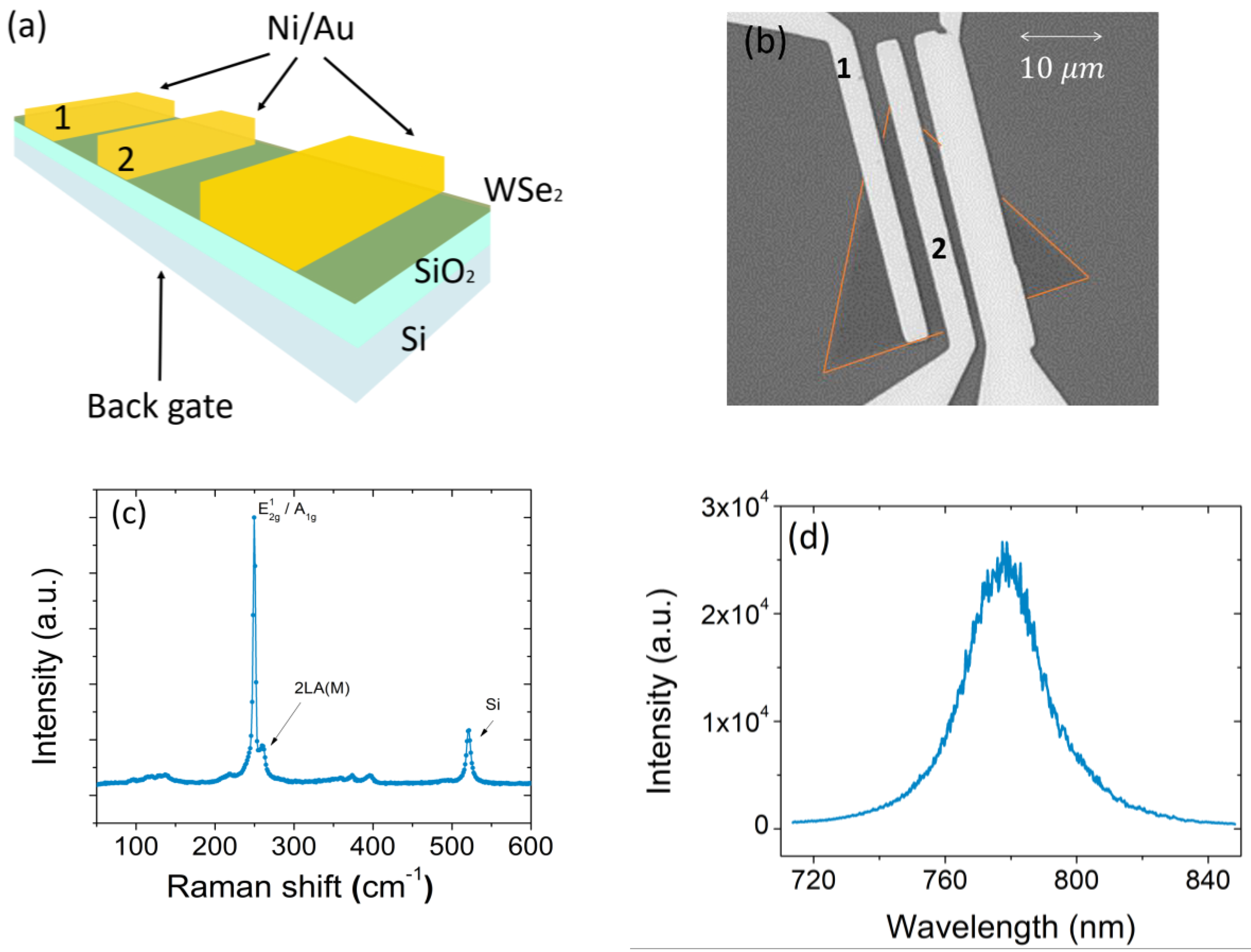
A schematic of the back-gated FET device and a scanning electron microscope top-view of a monolayer with evaporated Ni/Au contacts, made by use of e-beam lithography, are shown in Figure 1a,b. In the following, the transistor characterization refers to contact 1 and 2, which define a device with channel length and mean width (Figure 1b). The electrical analyses are performed using a Keithley 4200 SCS (semiconductor characterization system, Tektronix Inc., Beaverton, OR, USA) connected with a Janis ST-500 probe station (Janis Research Company LLC, Woburn, MA, USA), equipped with four probes used for the electrical connection to the drain and source Ni/Au terminals and to the Si back-gate of the device.
Raman and photoluminescence (PL) spectra were acquired using a WITec Alpha 300 tool (WITec GmbH, Ulm, Germany) with a 532 nm excitation laser. The Raman spectrum of the , displayed in Figure 1c, exhibits two peaks around and , corresponding to an overlapping contribution from the in-plane vibrations of W and Se atoms (E12g) and out-of-plane vibrations of Se atoms (A1g), and to a second-order resonant Raman mode due to LA phonons at the M point in the Brillouin zone [42,43], respectively. The peak frequency positions are typical of a monolayer of thickness [29]. The monolayer structure of the flake is further confirmed by the PL spectrum of Figure 1d, which shows an intense and narrow peak with maximum at and FWHM of Such a peak corresponds to a bandgap of , a value closer to that of a monolayer than to that of a bilayer. Hence, both Raman and PL spectra indicate that the flake is a monolayer.
3. Results and Discussion
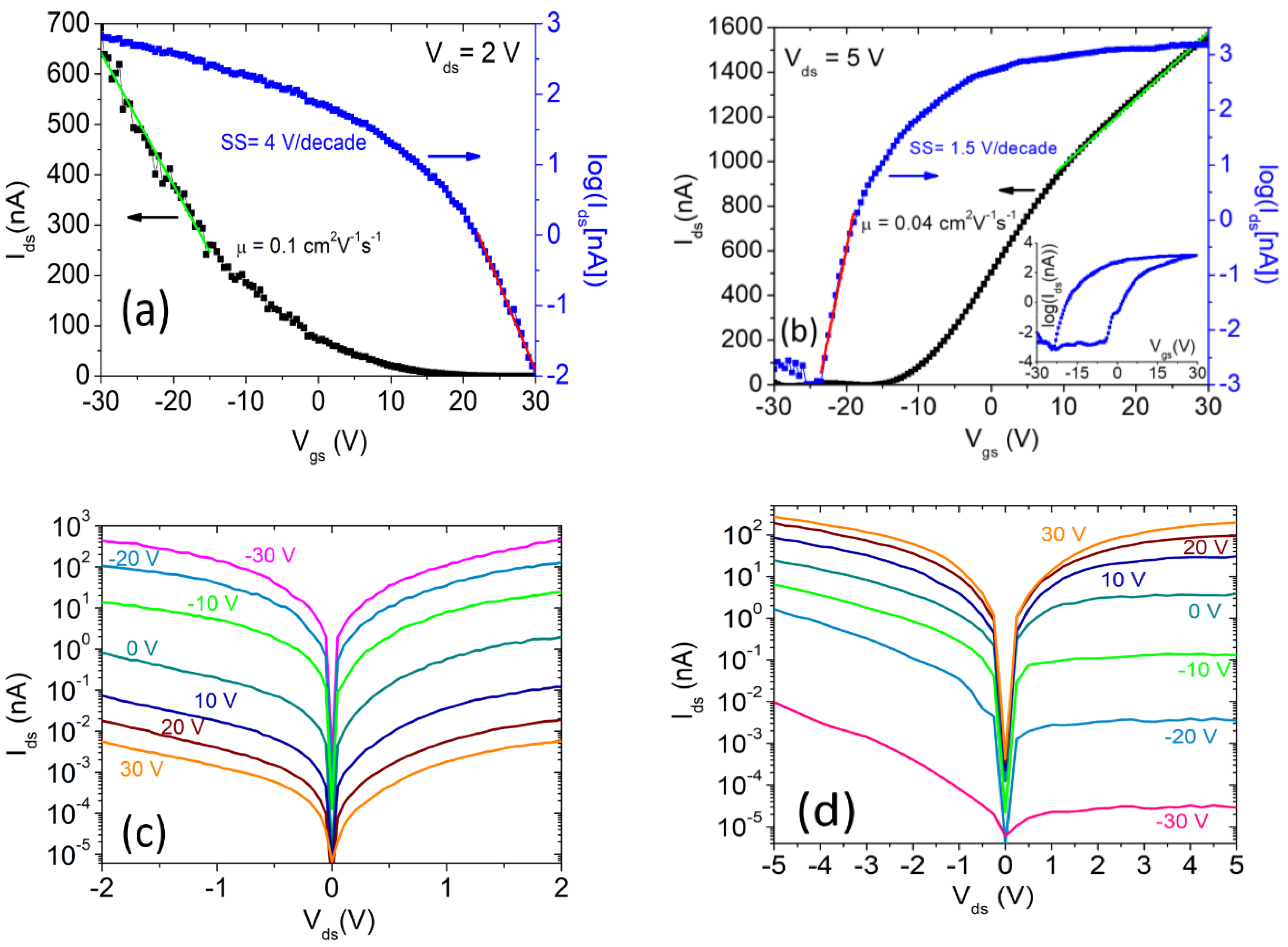
We start the transistor characterization by comparing the device I-V curves with and without a PMMA coating layer, which was used to protect the transistor channel from residue and adsorbates [44,45]. It has been observed that a PMMA film, or even only residue of it, can cause p-type doping of graphene and other 2D channels due to the presence of oxygen. Here, we report a similar effect for CVD-grown FETs, measured at , and .
The PMMA-covered devices behave like p-type transistors, as can be seen from the transfer curves of Figure 2a which show high channel current (on-state of the FET) at negative gate voltages, . The p-type conduction is explained considering the charge transfer to oxygen which, acting as electron capture center, suppresses the free electron density and enhances the hole concentration in the channel. Furthermore, the transition of the channel to p-type could cause a depinning of the Fermi level and facilitate hole injection at the contacts (indeed, in TMDs, Fermi level pinning often occurs close to the minimum of the conduction band) [36,46,47,48]. After the removal of the PMMA by immersion in acetone, a dramatic change to n-type behavior appeared, with the on-state at , as shown in Figure 2b. A similar effect has been reported in literature [32,49] for exfoliated flakes on an substrate covered by -doped PMMA.
The corresponding output characteristics are reported in Figure 2c,d. Both plots show non-linear behavior for the device in the on state with increasing positive-negative asymmetry when the device approaches the off state. This points to the presence of Schottky barriers at the contacts, possibly with slightly different heights [37,50].
For increasing , the channel current at constant shows an exponential dependence (below the threshold region) followed by a linear or power law behavior (above the threshold region).
A quadratic behavior is particularly evident in the transfer characteristic of Figure 2a, even though the transistor is operated in the triode region. The parabolic dependence of on can be ascribed to the linear gate-voltage dependence of the mobility [51,52], which defines the drain current as:
with:
in which represents the mobility per unit gate voltage and is the threshold voltage. The -dependent mobility can be explained by considering that the increasing carrier density becomes more effective at screening Coulomb scattering or in filling trap states at higher , thus resulting in enhanced mobility.
The dependence of the mobility on the gate voltage can be established by extracting it in the usual way using:
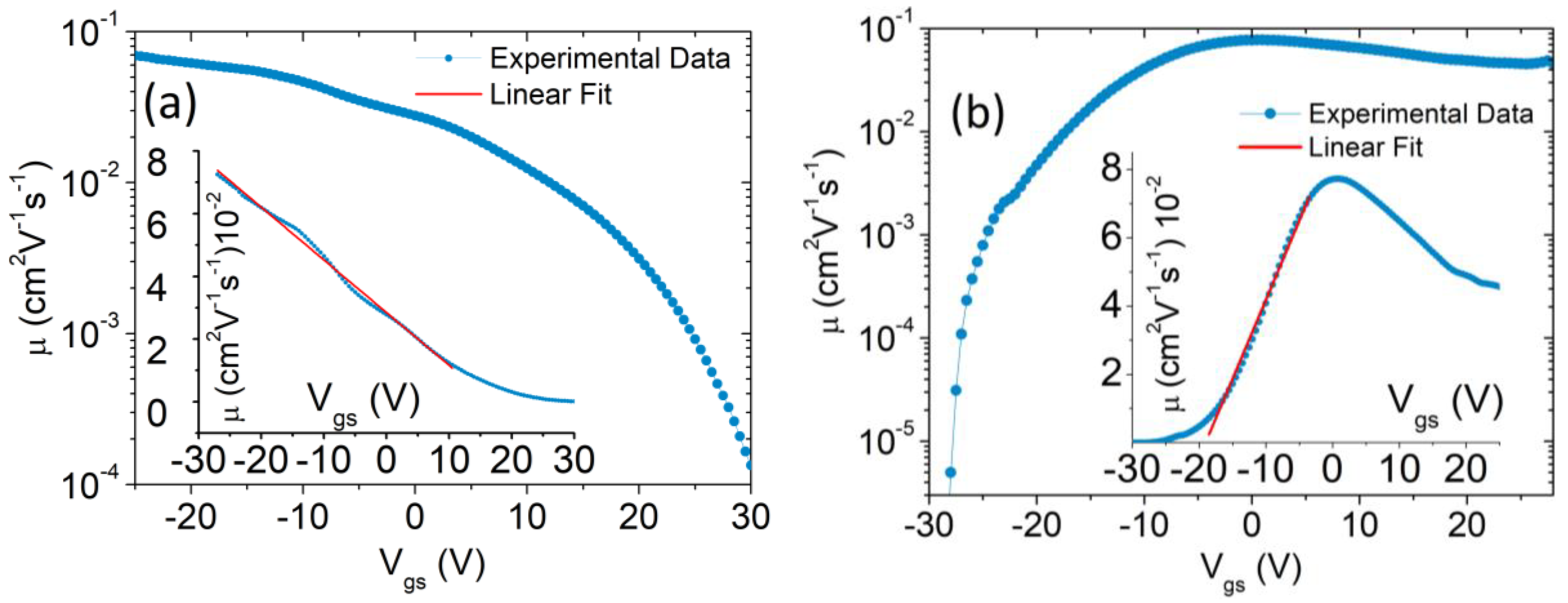
Figure 3a,b show the curves on logarithmic and linear (insets) scales obtained from Equation (3) and the data of Figure 2, for the devices with and without PMMA, respectively. These confirm a linear dependence of on over a certain range. Remarkably, for the device with removed PMMA, the mobility shows the typical decrease observed in common FETs due to increased scattering suffered by carriers attracted at the channel/dielectric interface at higher gate voltages.
By neglecting the dependence of the mobility, as is usually done in the literature, can be obtained by fitting a straight line to the transfer characteristics, as shown in Figure 2a,b.
By this method, we estimate an electron mobility of for the n-type transistor without PMMA, consistent with other works with on [41], and a hole mobility of for the PMMA-covered p-type transistor. We notice that, although a different channel carrier concentration might contribute to this difference, these values are consistent with the higher hole mobility in reported elsewhere [29,32,45]. The low mobility indicates a high density of trap states, which are also responsible for the hysteretic behavior of the transfer characteristic shown in the inset of Figure 2b. The hysteresis is caused by trapping and detrapping of charge carriers, whose potential adds to that of the back-gate [51,52,53,54].
The subthreshold swing, , is and , for the p-type and n-type transistor, respectively. The different results from a different trap density at the interface, implying a higher trap density when the channel is covered by PMMA, which acts as a second interface [55,56].
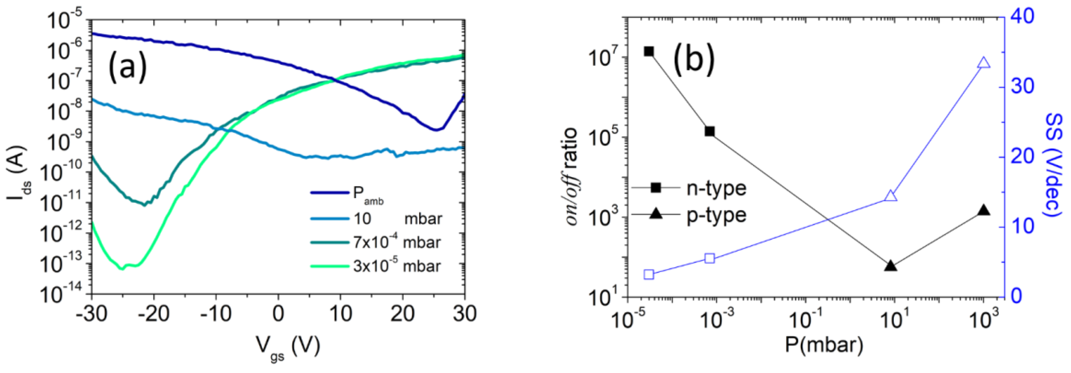
After the removal of the polymeric film and exposure of the device to air for a few days, we observed a restoration of a prevailing p-type behavior due to and water adsorption on the surface and possible depinning of the Fermi level. We then studied the effect of dynamic pressure by increasing the vacuum level of the probe station chamber from atmosphere () to . As reported in Figure 4a, the transistor transfer characteristic changed again from p- to n-type with a gradual decrease of the subthreshold swing and an increase of the on/off ratio, as shown in Figure 4b. We attribute the polarity change to the desorption of adsorbed and to the consequent possible pinning of the Fermi level close to the minimum of the conduction band.
We then examined the temperature dependence of the transfer characteristics of the PMMA-free, n-type transistor at low pressure, which can be conveniently used to investigate the Schottky barrier for electrons at the contacts.
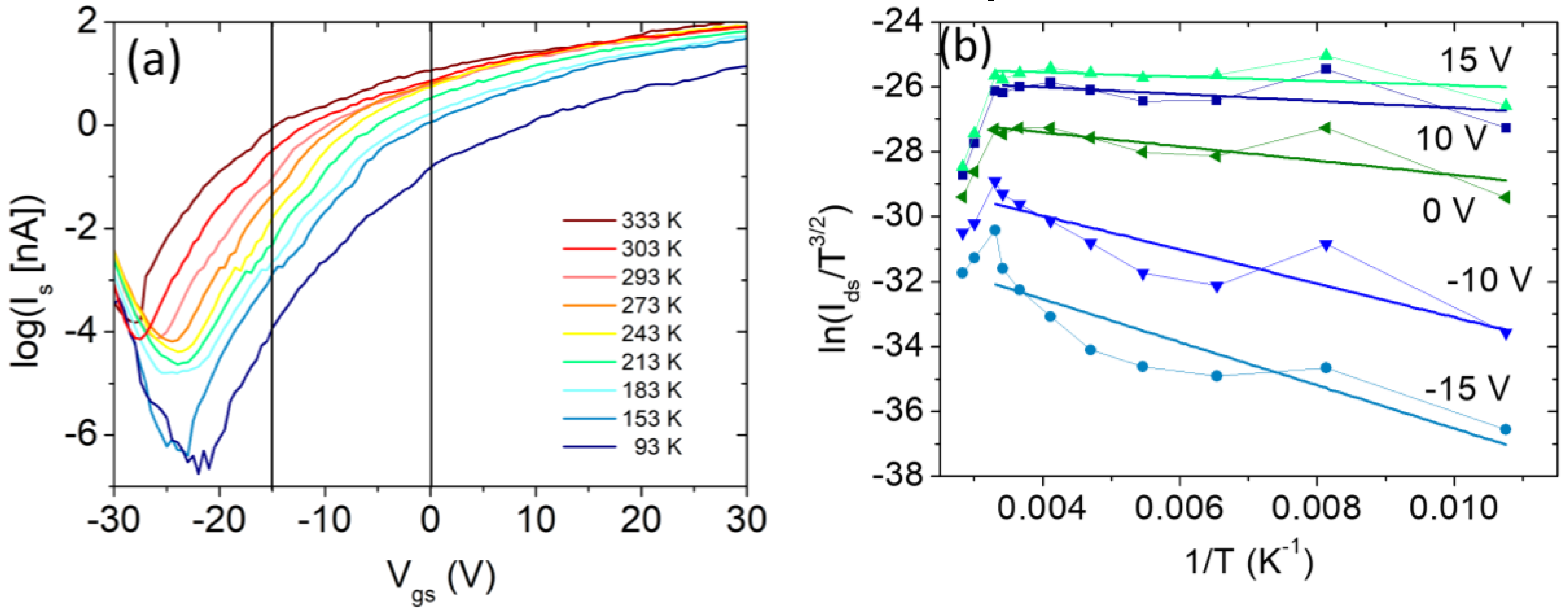
We extract the Schottky barrier at the flat-band condition from a plot of the Schottky barrier height as a function of for the device at a source-drain bias of 5 V (Figure 5). Given that the device is n-type, such a barrier refers to electron injection from the contacts and it is caused by the aforementioned pinning of the Fermi level close to the minimum of the conduction band. Measuring the characteristics of the device at several temperatures (Figure 5a) and extracting datasets at given gate voltages (examples are marked by the vertical lines in Figure 5a), we constructed the Arrhenius plot of Figure 5b, showing the curves at a representative subset of values. We assumed that the contacts behave as two back-to-back Schottky junctions, where the current is controlled by the reverse-biased junction and is written as:
where is the Boltzmann constant, is the absolute temperature, and is the Schottky barrier height [30,57,58]. According to equation (4), a linear fit of vs for each dataset in Figure 5b yields a Schottky barrier The so-obtained relationship is displayed in Figure 5c and can be divided into three zones, each one corresponding to a different transport regime, consistent with the behavior of the transfer characteristics of Figure 5a.
At low gate voltage the device is set in the off state and the transport is due to the thermal excitation of electrons over the barrier. The conduction-band level is gradually lowered by the increasing gate voltage, as sketched in the insets of Figure 5c. This results in a lowering of the barrier with a subsequent steep exponential rise of the current in the transfer characteristic (with slope in the ideal case). When the gate voltage is further increased the device reaches the flat band condition (), which sometimes appears in the subthreshold part of the transfer characteristics as a sudden change of slope; for the device enters the so-called Schottky regime which includes part of the downward bended region of curves and is characterized by thermionic emission and field emission. Finally, at higher , tunneling through the thinned barrier becomes the dominant conduction mechanism and the device reaches the above threshold region with a linear, or power-law, dependence.
The gate voltage that corresponds to is identified by the change of slope in the plot at lower . The corresponding to is the so-called Schottky barrier height at the flat-band (or simply Schottky barrier). From the plot in Figure 5c, its value is , confirming the presence of a barrier at the Ni-contacts, inferred from the asymmetric output characteristics of Figure 2.
Figure 5d shows the temperature-dependent behavior of the threshold voltage , which has been extracted assuming a quadratic law as expressed by Equation (1) and (2). The decrease in is easily explained by considering that the increasing temperature accelerates the transition from the Schottky to the power-law (above threshold) regime; furthermore, the plot seems to indicate a change of slope above room temperature.
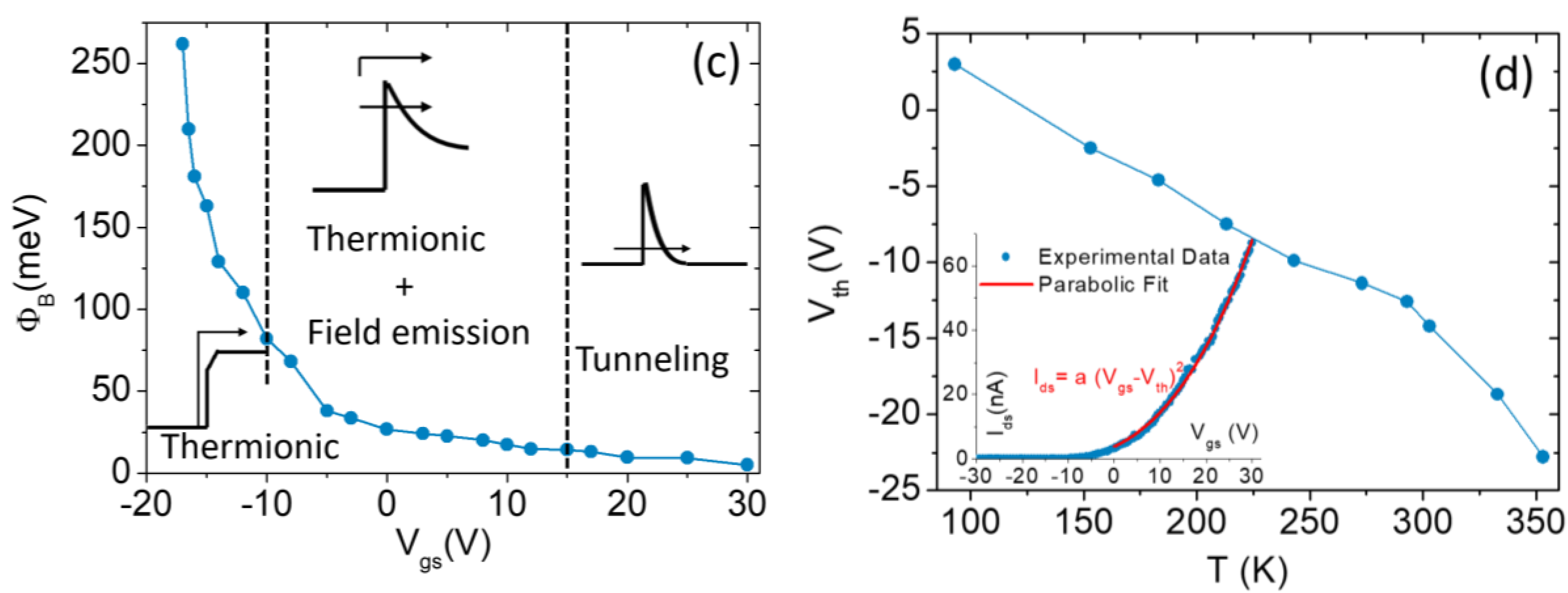
Figure 6a reports the temperature-dependent behavior of the mobility, , at obtained from the quadratic fit of the curves.
The mobility increases for and decreases for , behavior typical of semiconductor materials, indicating that charged-impurity Coulomb scattering dominates at lower temperatures, while phonon scattering becomes the conduction-limiting mechanism at high temperature [44].
The subthreshold swing has a dependence on temperature that can be simplified with the following expression:
where is the body factor which is related to the interface trap (), and channel depletion layer () capacitances by:
Figure 6b confirms the linear dependence (Equation 5) but shows an unexpected rise above room temperature. The deviation from Equation (5) behavior at high temperature is a consequence of the low Schottky barrier which becomes less effective above room temperature (), resulting in an increase of the subthreshold current leakage.
Assuming that the monolayer channel is fully depleted, i.e. that , from the fit of the experimental data with Equation (5), we obtain a and an interface trap density , which is consistent with previous results reported in the literature [59].
The presence of such a density of trap states explains the observed hysteretic behavior of the transfer characteristic, displayed in the inset of Figure 2b [52]. It also affects the electrical response of the device under illumination.
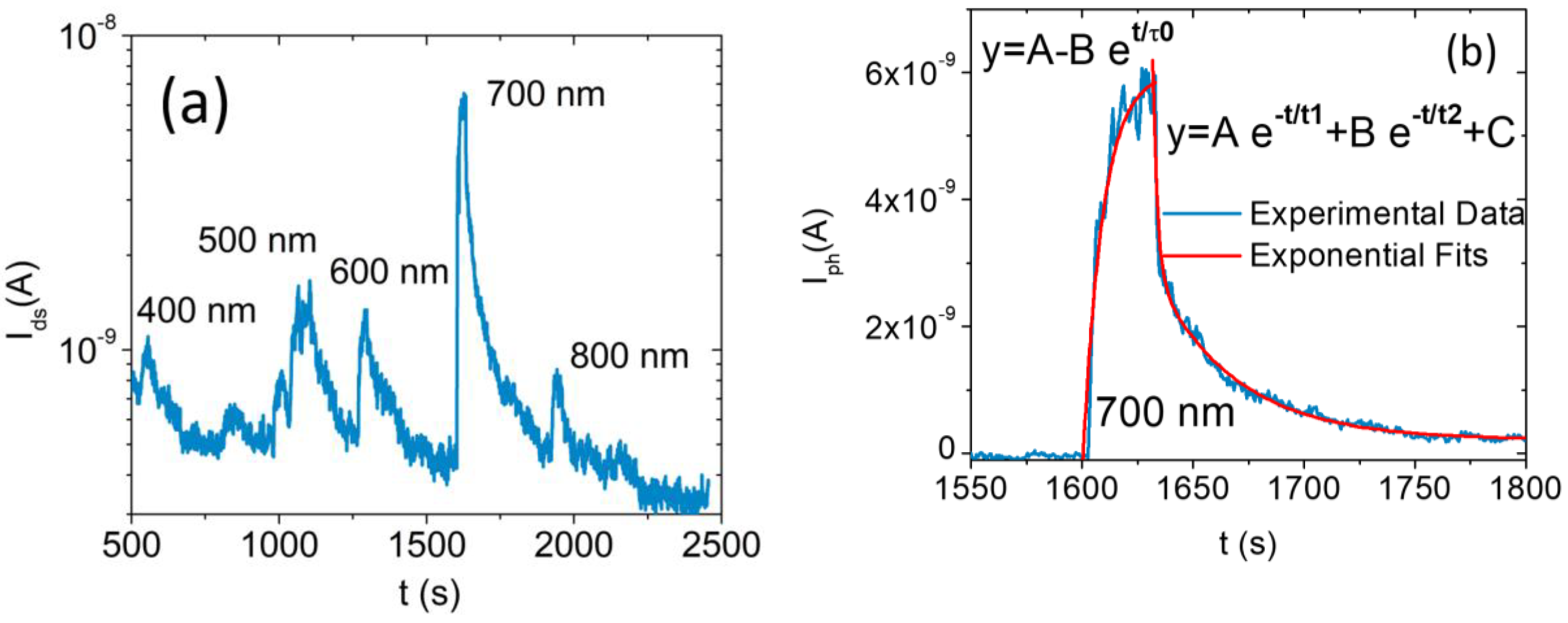
We performed photocurrent measurements with light at different wavelengths, selected by filtering a supercontinuous laser source (NKT Photonics, Superk Compact, wavelength ranging from 450 nm to 2400 nm, total output power of ) using pass-band filters with 50 nm bandwidth. Figure 7a shows the photoresponse of the FET to laser light pulses of 30 s for five different wavelengths.
The photocurrent exhibits a higher peak at the wavelength of 700 nm (photon energy 1.7 eV), which is slightly above the bandgap of a monolayer, supporting the Raman and the PL spectroscopy assignment of the single-layer nature of the channel.
Figure 7b reports the photocurrent, , obtained in response to a laser pulse of at a wavelength of , and an optical power . It corresponds to a peak with rising time and a double exponential decay with times and , indicating the presence of faster and slower traps [60]. Such features are consistent with a photoresponse decay longer than 5 s for quasi-ohmic contacts measured on similar FETs [61,62]. Indeed, we notice that the contact type can play an important role in the response time of phototransistors and that reduced times have been reported for Schottky contacts [61,62].
Furthermore, we estimate a photoresponsivity (Figure 7b):
where is the incident power. This is in good agreement with the previously reported value of obtained at 750 nm [62]. Such a responsivity is competitive with solid state devices on the market and, despite the ultrathin nature of the absorber, confirms the excellent photoresponse of monolayer due to its direct bandgap [63,64].
4. Conclusions
We showed that different environmental conditions can have dramatic effects on the electrical properties of back-gated transistors with channels. In particular, we demonstrated that the removal of a polymer coating layer, as well as of oxygen and water adsorbates, can change the conduction from p- to n-type. From I-V characterization at different temperatures, we extracted the Schottky barrier height, which we studied as a function of the back-gate voltage. We reported and discussed a change in the temperature behavior of the mobility and the subthreshold swing. Finally, we studied the photoresponse of the device to selected laser wavelengths achieving a responsivity competitive with solid-state devices on the market.
Author Contributions
F.U. and A.D.B. wrote the paper; A.D.B. and F.U. conceived and designed the experiments; F.U. and L.P. performed the experiments; F.U., N.M.E., and A.D.B. analyzed the data; and N.M., A.D.B., and N.M.E. contributed reagents/materials/analysis tools.
Funding
This research was funded by Regione Campania grant “POR Campania FSE 2014–2020, Asse III Ob. specifico l4, D.D. n. 80 del 31/05/2016”, by CNR-SPIN grant “SEED Project 2017” and by Science Foundation Ireland grant number: 15/SIRG/3329.
Conflicts of Interest
The authors declare no conflict of interest.
References
- Georgiou, T.; Jalil, R.; Belle, B.D.; Britnell, L.; Gorbachev, R.V.; Morozov, S.V.; Kim, Y.-J.; Gholinia, A.; Haigh, S.J.; Makarovsky, O.; et al. Vertical field-effect transistor based on graphene–WS2 heterostructures for flexible and transparent electronics. Nat. Nanotechnol. 2012, 8, 100–103. [Google Scholar] [CrossRef] [PubMed]
- Liu, H.; Neal, A.T.; Ye, P.D. Channel length scaling of MoS2 MOSFETs. ACS Nano 2012, 6, 8563–8569. [Google Scholar] [CrossRef] [PubMed]
- Lopez-Sanchez, O.; Lembke, D.; Kayci, M.; Radenovic, A.; Kis, A. Ultrasensitive photodetectors based on monolayer MoS2. Nat. Nanotechnol. 2013, 8, 497. [Google Scholar] [CrossRef] [PubMed]
- Pospischil, A.; Furchi, M.M.; Mueller, T. Solar-energy conversion and light emission in an atomic monolayer p–n diode. Nat. Nanotechnol. 2014, 9, 257. [Google Scholar] [CrossRef] [PubMed]
- Radisavljevic, B.; Radenovic, A.; Brivio, J.; Giacometti, V.; Kis, A. Single-layer MoS2 transistors. Nat. Nanotechnol. 2011, 6, 147. [Google Scholar] [CrossRef] [PubMed]
- Baugher, B.W.H.; Churchill, H.O.H.; Yang, Y.; Jarillo-Herrero, P. Optoelectronic devices based on electrically tunable p–n diodes in a monolayer dichalcogenide. Nat. Nanotechnol. 2014, 9, 262. [Google Scholar] [CrossRef] [PubMed]
- Ross, J.S.; Klement, P.; Jones, A.M.; Ghimire, N.J.; Yan, J.; Mandrus, D.G.; Taniguchi, T.; Watanabe, K.; Kitamura, K.; Yao, W.; et al. Electrically tunable excitonic light-emitting diodes based on monolayer WSe2 p–n junctions. Nat. Nanotechnol. 2014, 9, 268. [Google Scholar] [CrossRef] [PubMed]
- Liu, W.; Kang, J.; Sarkar, D.; Khatami, Y.; Jena, D.; Banerjee, K. Role of metal contacts in designing high-performance monolayer n-type WSe2 field effect transistors. Nano Lett. 2013, 13, 1983–1990. [Google Scholar] [CrossRef] [PubMed]
- Guo, Y.; Han, Y.; Li, J.; Xiang, A.; Wei, X.; Gao, S.; Chen, Q. Study on the resistance distribution at the contact between molybdenum disulfide and metals. ACS Nano 2014, 8, 7771–7779. [Google Scholar] [CrossRef] [PubMed]
- Rai, A.; Movva, C.H.; Roy, A.; Taneja, D.; Chowdhury, S.; Banerjee, K.S. Progress in contact, doping and mobility engineering of MoS2: An atomically thin 2D semiconductor. Crystals 2018, 8, 316. [Google Scholar] [CrossRef]
- Dean, C.R.; Young, A.F.; Meric, I.; Lee, C.; Wang, L.; Sorgenfrei, S.; Watanabe, K.; Taniguchi, T.; Kim, P.; Shepard, K.L.; et al. Boron nitride substrates for high-quality graphene electronics. Nat. Nanotechnol. 2010, 5, 722. [Google Scholar] [CrossRef] [PubMed]
- Chen, J.-H.; Jang, C.; Adam, S.; Fuhrer, M.S.; Williams, E.D.; Ishigami, M. Charged-impurity scattering in graphene. Nat. Phys. 2008, 4, 377. [Google Scholar] [CrossRef]
- Lin, J.; Zhong, J.; Zhong, S.; Li, H.; Zhang, H.; Chen, W. Modulating electronic transport properties of MoS2 field effect transistor by surface overlayers. Appl. Phys. Lett. 2013, 103, 063109. [Google Scholar] [CrossRef]
- Mouri, S.; Miyauchi, Y.; Matsuda, K. Tunable photoluminescence of monolayer MoS2 via chemical doping. Nano Lett. 2013, 13, 5944–5948. [Google Scholar] [CrossRef] [PubMed]
- Late, D.J.; Liu, B.; Matte, H.S.S.R.; Dravid, V.P.; Rao, C.N.R. Hysteresis in single-layer MoS2 field effect transistors. ACS Nano 2012, 6, 5635–5641. [Google Scholar] [CrossRef] [PubMed]
- Roy, A.; Ghosh, R.; Rai, A.; Sanne, A.; Kim, K.; Movva, H.C.P.; Dey, R.; Pramanik, T.; Chowdhury, S.; Tutuc, E.; et al. Intra-domain periodic defects in monolayer MoS2. Appl. Phys. Lett. 2017, 110, 201905. [Google Scholar] [CrossRef]
- Zhao, P.; Kiriya, D.; Azcatl, A.; Zhang, C.; Tosun, M.; Liu, Y.-S.; Hettick, M.; Kang, J.S.; McDonnell, S.; KC, S.; et al. Air stable p-doping of WSe2 by covalent functionalization. ACS Nano 2014, 8, 10808–10814. [Google Scholar] [CrossRef] [PubMed]
- Urban, F.; Passacantando, M.; Giubileo, F.; Iemmo, L.; Di Bartolomeo, A. Transport and field emission properties of MoS2 bilayers. Nanomaterials 2018, 8, 151. [Google Scholar] [CrossRef] [PubMed]
- Fang, H.; Tosun, M.; Seol, G.; Chang, T.C.; Takei, K.; Guo, J.; Javey, A. Degenerate n-doping of few-layer transition metal dichalcogenides by potassium. Nano Lett. 2013, 13, 1991–1995. [Google Scholar] [CrossRef] [PubMed]
- Rai, A.; Valsaraj, A.; Movva, H.C.P.; Roy, A.; Ghosh, R.; Sonde, S.; Kang, S.; Chang, J.; Trivedi, T.; Dey, R.; et al. Air stable doping and intrinsic mobility enhancement in monolayer molybdenum disulfide by amorphous titanium suboxide encapsulation. Nano Lett. 2015, 15, 4329–4336. [Google Scholar] [CrossRef] [PubMed]
- Tongay, S.; Zhou, J.; Ataca, C.; Lo, K.; Matthews, T.S.; Li, J.; Grossman, J.C.; Wu, J. Thermally driven crossover from indirect toward direct bandgap in 2D semiconductors: MoSe2 versus MoS2. Nano Lett. 2012, 12, 5576–5580. [Google Scholar] [CrossRef] [PubMed]
- Jariwala, D.; Sangwan, V.K.; Late, D.J.; Johns, J.E.; Dravid, V.P.; Marks, T.J.; Lauhon, L.J.; Hersam, M.C. Band-like transport in high mobility unencapsulated single-layer MoS2 transistors. Appl. Phys. Lett. 2013, 102, 173107. [Google Scholar] [CrossRef]
- Valsaraj, R.A.; Movva, H.C.P.; Roy, A.; Tutuc, E.; Register, L.F.; Banerjee, S.K. Interfacial-oxygen-vacancy mediated doping of MoS2 by high-κ dielectrics. In 2015 73rd Annual Device Research Conference (DRC), Proceedings of the 73rd Annual Device Research Conference (DRC), Columbus, OH, USA, 21–24 June 2015; IEEE: Piscataway, NJ, USA, 06 August 2015; pp. 189–190. [Google Scholar]
- Desai, S.B.; Madhvapathy, S.R.; Sachid, A.B.; Llinas, J.P.; Wang, Q.; Ahn, G.H.; Pitner, G.; Kim, M.J.; Bokor, J.; Hu, C.; et al. MoS2 transistors with 1-nanometer gate lengths. Science 2016, 354, 99. [Google Scholar] [CrossRef] [PubMed]
- Yang, L.M.; Majumdar, K.; Du, Y.; Liu, H.; Wu, H.; Hatzistergos, M.; Hung, P.Y.; Tieckelmann, R.; Tsai, W.; Hobbs, C.; et al. High-performance MoS2 field-effect transistors enabled by chloride doping: Record low contact resistance (0.5 kΩ·µm) and record high drain current (460 µA/µm). In 2014 Symposium on VLSI Technology (VLSI-Technology): Digest of Technical Papers, Proceedings of 2014 Symposium on VLSI Technology, Honolulu, HI, USA, 9–12 June 2014; IEEE: Piscataway, NJ, USA, 11 September 2014; pp. 1–2. [Google Scholar]
- Allain, A.; Kis, A. Electron and hole mobilities in single-layer WSe2. ACS Nano 2014, 8, 7180–7185. [Google Scholar] [CrossRef]
- Zhao, W.; Ghorannevis, Z.; Chu, L.; Toh, M.; Kloc, C.; Tan, P.-H.; Eda, G. Evolution of electronic structure in atomically thin sheets of WS2 and WSe2. ACS Nano 2013, 7, 791–797. [Google Scholar] [CrossRef]
- Pradhan, N.R.; Rhodes, D.; Memaran, S.; Poumirol, J.M.; Smirnov, D.; Talapatra, S.; Feng, S.; Perea-Lopez, N.; Elias, A.L.; Terrones, M.; et al. Hall and field-effect mobilities in few layered p-WSe2 field-effect transistors. Sci. Rep. 2015, 5, 8979. [Google Scholar] [CrossRef] [PubMed]
- Fang, H.; Chuang, S.; Chang, T.C.; Takei, K.; Takahashi, T.; Javey, A. High-performance single layered WSe2 p-FETs with chemically doped contacts. Nano Lett. 2012, 12, 3788–3792. [Google Scholar] [CrossRef] [PubMed]
- Das, S.; Appenzeller, J. WSe2 field effect transistors with enhanced ambipolar characteristics. Appl. Phys. Lett. 2013, 103, 103501. [Google Scholar] [CrossRef]
- Liu, B.; Fathi, M.; Chen, L.; Abbas, A.; Ma, Y.; Zhou, C. Chemical vapor deposition growth of monolayer WSe2 with tunable device characteristics and growth mechanism study. ACS Nano 2015, 9, 6119–6127. [Google Scholar] [CrossRef]
- Yu, L.; Zubair, A.; Santos, E.J.G.; Zhang, X.; Lin, Y.; Zhang, Y.; Palacios, T. High-performance WSe2 complementary metal oxide semiconductor technology and integrated circuits. Nano Lett. 2015, 15, 4928–4934. [Google Scholar] [CrossRef]
- Tosun, M.; Chuang, S.; Fang, H.; Sachid, A.B.; Hettick, M.; Lin, Y.; Zeng, Y.; Javey, A. High-gain inverters based on WSe2 complementary field-effect transistors. ACS Nano 2014, 8, 4948–4953. [Google Scholar] [CrossRef] [PubMed]
- Das, S.; Dubey, M.; Roelofs, A. High gain, low noise, fully complementary logic inverter based on bi-layer WSe2 field effect transistors. Appl. Phys. Lett. 2014, 105, 083511. [Google Scholar] [CrossRef]
- Giubileo, F.; Di Bartolomeo, A. The role of contact resistance in graphene field-effect devices. Prog. Surf. Sci. 2017, 92, 143–175. [Google Scholar] [CrossRef] [Green Version]
- Di Bartolomeo, A.; Giubileo, F.; Romeo, F.; Sabatino, P.; Carapella, G.; Iemmo, L.; Schroeder, T.; Lupina, G. Graphene field effect transistors with niobium contacts and asymmetric transfer characteristics. Nanotechnology 2015, 26, 475202. [Google Scholar] [CrossRef] [PubMed] [Green Version]
- Di Bartolomeo, A.; Grillo, A.; Urban, F.; Iemmo, L.; Giubileo, F.; Luongo, G.; Amato, G.; Croin, L.; Sun, L.; Liang, S.J.; et al. Asymmetric schottky contacts in bilayer MoS2 field effect transistors. Adv. Funct. Mater. 2018, 28, 1800657. [Google Scholar] [CrossRef]
- Chuang, H.-J.; Tan, X.; Ghimire, N.J.; Perera, M.M.; Chamlagain, B.; Cheng, M.M.-C.; Yan, J.; Mandrus, D.; Tománek, D.; Zhou, Z. High mobility WSe2 p- and n-type field-effect transistors contacted by highly doped graphene for low-resistance contacts. Nano Lett. 2014, 14, 3594–3601. [Google Scholar] [CrossRef] [PubMed]
- Borin Barin, G.; Song, Y.; de Fátima Gimenez, I.; Souza Filho, A.G.; Barreto, L.S.; Kong, J. Optimized graphene transfer: Influence of polymethylmethacrylate (PMMA) layer concentration and baking time on graphene final performance. Carbon 2015, 84, 82–90. [Google Scholar] [CrossRef]
- Son, B.H.; Kim, H.S.; Jeong, H.; Park, J.-Y.; Lee, S.; Ahn, Y.H. Electron beam induced removal of PMMA layer used for graphene transfer. Sci. Rep. 2017, 7, 18058. [Google Scholar] [CrossRef] [PubMed] [Green Version]
- O’Brien, M.; McEvoy, N.; Hallam, T.; Kim, H.-Y.; Berner, N.C.; Hanlon, D.; Lee, K.; Coleman, J.N.; Duesberg, G.S. Transition metal dichalcogenide growth via close proximity precursor supply. Sci. Rep. 2014, 4, 7374. [Google Scholar] [CrossRef] [PubMed]
- Zhao, W.; Ghorannevis, Z.; Amara, K.K.; Pang, J.R.; Toh, M.; Zhang, X.; Kloc, C.; Tan, P.H.; Eda, G. Lattice dynamics in mono- and few-layer sheets of WS2 and WSe2. Nanoscale 2013, 5, 9677–9683. [Google Scholar] [CrossRef] [PubMed]
- O’Brien, M.; McEvoy, N.; Hanlon, D.; Hallam, T.; Coleman, J.N.; Duesberg, G.S. Mapping of low-frequency raman modes in CVD-grown transition metal dichalcogenides: Layer number, stacking orientation and resonant effects. Sci. Rep. 2016, 6, 19476. [Google Scholar] [CrossRef] [PubMed]
- Ovchinnikov, D.; Allain, A.; Huang, Y.-S.; Dumcenco, D.; Kis, A. Electrical transport properties of single-layer WS2. ACS Nano 2014, 8, 8174–8181. [Google Scholar] [CrossRef] [PubMed]
- Schmidt, H.; Giustiniano, F.; Eda, G. Electronic transport properties of transition metal dichalcogenide field-effect devices: Surface and interface effects. Chem. Soc. Rev. 2015, 44, 7715–7736. [Google Scholar] [CrossRef] [PubMed]
- Pandey, A.; Prasad, A.; Moscatello, J.; Ulmen, B.; Yap, Y.K. Enhanced field emission stability and density produced by conical bundles of catalyst-free carbon nanotubes. Carbon 2010, 48. [Google Scholar] [CrossRef]
- Di Bartolomeo, A.; Giubileo, F.; Iemmo, L.; Romeo, F.; Russo, S.; Unal, S.; Passacantando, M.; Grossi, V.; Cucolo, A.M. Leakage and field emission in side-gate graphene field effect transistors. Appl. Phys. Lett. 2016, 109, 023510. [Google Scholar] [CrossRef]
- Pirkle, A.; Chan, J.; Venugopal, A.; Hinojos, D.; Magnuson, C.W.; McDonnell, S.; Colombo, L.; Vogel, E.M.; Ruoff, R.S.; Wallace, R.M. The effect of chemical residues on the physical and electrical properties of chemical vapor deposited graphene transferred to SiO2. Appl. Phys. Lett. 2011, 99, 122108. [Google Scholar] [CrossRef]
- Movva, H.C.P.; Rai, A.; Kang, S.; Kim, K.; Fallahazad, B.; Taniguchi, T.; Watanabe, K.; Tutuc, E.; Banerjee, S.K. High-mobility holes in dual-gated WSe2 field-effect transistors. ACS Nano 2015, 9, 10402–10410. [Google Scholar] [CrossRef] [PubMed]
- Di Bartolomeo, A.; Urban, F.; Passacantando, M.; McEvoy, N.; Peters, L.; Iemmo, L.; Luongo, G.; Romeo, F.; Giubileo, F. A WSe2 vertical field emission transistor. arXiv, 2018; arXiv:1808.02127. [Google Scholar]
- Gupta, D.; Katiyar, M.; Gupta, D. Mobility estimation incorporating the effects of contact resistance and gate voltage dependent mobility in top contact organic thin film transistors. In Proceedings of the ASID 2006, New Delhi, India, 8–12 October 2006; pp. 425–428. [Google Scholar]
- Di Bartolomeo, A.; Genovese, L.; Giubileo, F.; Iemmo, L.; Luongo, G.; Tobias, F.; Schleberger, M. Hysteresis in the transfer characteristics of MoS2 transistors. 2D Materials 2018, 5, 015014. [Google Scholar] [CrossRef]
- Guo, Y.; Wei, X.; Shu, J.; Liu, B.; Yin, J.; Guan, C.; Han, Y.; Gao, S.; Chen, Q. Charge trapping at the MoS2-SiO2 interface and its effects on the characteristics of MoS2 metal-oxide-semiconductor field effect transistors. Appl. Phys. Lett. 2015, 106, 103109. [Google Scholar] [CrossRef]
- Di Bartolomeo, A.; Yang, Y.; Rinzan, M.B.M.; Boyd, A.K.; Barbara, P. Record endurance for single-walled carbon nanotube–based memory cell. Nanoscale Res. Lett. 2010, 5, 1852. [Google Scholar] [CrossRef] [PubMed]
- Gatensby, R.; Hallam, T.; Lee, K.; McEvoy, N.; Duesberg, G.S. Investigations of vapour-phase deposited transition metal dichalcogenide films for future electronic applications. Solid State Electron. 2016, 125, 39–51. [Google Scholar] [CrossRef]
- Giubileo, F.; Iemmo, L.; Passacantando, M.; Urban, F.; Luongo, G.; Sun, L.; Amato, G.; Enrico, E.; Di Bartolomeo, A. Effect of electron irradiation on the transport and field emission properties of few-layer MoS2 field effect transistors. arXiv, 2018; arXiv:1808.01185. [Google Scholar]
- Das, S.; Chen, H.-Y.; Penumatcha, A.V.; Appenzeller, J. High performance multilayer MoS2 transistors with scandium contacts. Nano Lett. 2013, 13, 100–105. [Google Scholar] [CrossRef] [PubMed]
- Houssa, M.; Dimoulas, A.; Molle, A. 2D Materials for Nanoelectronics. 2016. Available online: https://inn.demokritos.gr/wp-content/uploads/2016/05/Promo_K24702_Flyer.pdf (accessed on 1 October 2018).
- Wang, J.; Rhodes, D.; Feng, S.; Nguyen, M.A.T.; Watanabe, K.; Taniguchi, T.; Mallouk, T.E.; Terrones, M.; Balicas, L.; Zhu, J. Gate-modulated conductance of few-layer WSe2 field-effect transistors in the subgap regime: Schottky barrier transistor and subgap impurity states. Appl. Phys. Lett. 2015, 106, 152104. [Google Scholar] [CrossRef]
- Di Bartolomeo, A.; Genovese, L.; Foller, T.; Giubileo, F.; Luongo, G.; Croin, L.; Liang, S.-J.; Ang, L.K.; Schleberger, M. Electrical transport and persistent photoconductivity in monolayer MoS2 phototransistors. Nanotechnology 2017, 28, 214002. [Google Scholar] [CrossRef] [PubMed]
- Zhang, W.; Chiu, M.-H.; Chen, C.-H.; Chen, W.; Li, L.-J.; Wee, A.T.S. Role of metal contacts in high-performance phototransistors based on WSe2 monolayers. ACS Nano 2014, 8, 8653–8661. [Google Scholar] [CrossRef] [PubMed]
- Wang, T.; Andrews, K.; Bowman, A.; Hong, T.; Koehler, M.; Yan, J.; Mandrus, D.; Zhou, Z.; Xu, Y.-Q. High-performance WSe2 phototransistors with 2D/2D ohmic contacts. Nano Lett. 2018, 18, 2766–2771. [Google Scholar] [CrossRef] [PubMed]
- Li, H.; Qin, M.; Wang, L.; Zhai, X.; Ren, R.; Hu, J. Total absorption of light in monolayer transition-metal dichalcogenides by critical coupling. Opt. Express 2017, 25, 31612–31621. [Google Scholar] [CrossRef] [PubMed]
- Frindt, R.F. The optical properties of single crystals of WSe2 and MoTe2. J. Phys. Chem. Solids 1963, 24, 1107–1108. [Google Scholar] [CrossRef]
Figure 1.
Schematic diagram (a) and optical microscope image (b) of the back gate FET transistor. Raman (c) and photoluminescence (d) spectra of the flake.
Figure 1.
Schematic diagram (a) and optical microscope image (b) of the back gate FET transistor. Raman (c) and photoluminescence (d) spectra of the flake.

Figure 2.
Transfer characteristics ( curves) obtained at a drain voltage bias for the device covered with PMMA (a) and after the removal of PMMA (b) at . The inset shows a complete cycle with the gate voltage swept forward and backward. Output characteristics ( curves) at different gate voltages for the device with (c) and without (d) PMMA. For the uncovered device, the drain bias was increased from to to better characterize the above-threshold region.

Figure 3.
Mobility versus gate voltage on a logarithmic scale for the flake covered (a) and uncovered (b) by PMMA. The inset graphs show the mobility on a linear scale.
Figure 3.
Mobility versus gate voltage on a logarithmic scale for the flake covered (a) and uncovered (b) by PMMA. The inset graphs show the mobility on a linear scale.

Figure 4.
(a) Transfer characteristics at different pressures from atmospheric value (blue curve) to mbar (light green curve) (b) On/Off ratio (full marks, left scale) and subthreshold swing (empty marks, right scale) as a function of the chamber pressure.
Figure 4.
(a) Transfer characteristics at different pressures from atmospheric value (blue curve) to mbar (light green curve) (b) On/Off ratio (full marks, left scale) and subthreshold swing (empty marks, right scale) as a function of the chamber pressure.

Figure 5.
(a) Transfer characteristic at several temperatures. (b) Arrhenius plot of the current at different temperatures corresponding to a subset of the gate voltages (two of these values are represented by the vertical lines in (a)). (c) Apparent Schottky barrier as a function of the gate voltage; the insets show the band alignment and the transport regimes at the Ni/WSe2 reverse-biased contact. (d) Threshold voltage as a function of the temperature; the inset shows, as an example, the parabolic fit of the curve at .


Figure 6.
Temperature dependence of (a) mobility per unit voltage and (b) subthreshold swing.

Figure 7.
(a) Drain-source current measured under 30 s laser pulses at different wavelengths (, ). (b) Photocurrent generated by a laser pulse at the wavelength of and optical power with exponential fits.
Figure 7.
(a) Drain-source current measured under 30 s laser pulses at different wavelengths (, ). (b) Photocurrent generated by a laser pulse at the wavelength of and optical power with exponential fits.

© 2018 by the authors. Licensee MDPI, Basel, Switzerland. This article is an open access article distributed under the terms and conditions of the Creative Commons Attribution (CC BY) license (http://creativecommons.org/licenses/by/4.0/).
Share and Cite
MDPI and ACS Style
Urban, F.; Martucciello, N.; Peters, L.; McEvoy, N.; Di Bartolomeo, A. Environmental Effects on the Electrical Characteristics of Back-Gated WSe2 Field-Effect Transistors. Nanomaterials 2018, 8, 901. https://doi.org/10.3390/nano8110901
AMA Style
Urban F, Martucciello N, Peters L, McEvoy N, Di Bartolomeo A. Environmental Effects on the Electrical Characteristics of Back-Gated WSe2 Field-Effect Transistors. Nanomaterials. 2018; 8(11):901. https://doi.org/10.3390/nano8110901
Chicago/Turabian StyleUrban, Francesca, Nadia Martucciello, Lisanne Peters, Niall McEvoy, and Antonio Di Bartolomeo. 2018. "Environmental Effects on the Electrical Characteristics of Back-Gated WSe2 Field-Effect Transistors" Nanomaterials 8, no. 11: 901. https://doi.org/10.3390/nano8110901
Note that from the first issue of 2016, this journal uses article numbers instead of page numbers. See further details here.