Review

Recent Advancement on the Optical Properties of Two-Dimensional Molybdenum Disulfide (MoS2) Thin Films

Department of Physics, Michigan Technological University, 1400 Townsend Drive, Houghton, MI 49931, USA
*
Author to whom correspondence should be addressed.
Photonics 2015, 2(1), 288-307; https://doi.org/10.3390/photonics2010288
Submission received: 20 January 2015 / Revised: 3 March 2015 / Accepted: 4 March 2015 / Published: 16 March 2015

Abstract

:
The emergence of two-dimensional (2D) materials has led to tremendous interest in the study of graphene and a series of mono- and few-layered transition metal dichalcogenides (TMDCs). Among these TMDCs, the study of molybdenum disulfide (MoS2) has gained increasing attention due to its promising optical, electronic, and optoelectronic properties. Of particular interest is the indirect to direct band-gap transition from bulk and few-layered structures to mono-layered MoS2, respectively. In this review, the study of these properties is summarized. The use of Raman and Photoluminescence (PL) spectroscopy of MoS2 has become a reliable technique for differentiating the number of molecular layers in 2D MoS2.

Graphical Abstract

1. Introduction

Many bulk crystals exhibit layered atomic structure with strong intra-layer bonds, but with weak van der Waals interaction between layers. Graphite is a representative example in which mechanical exfoliation of mono graphite layers has led to the discovery of graphene [1,2]. These exfoliated, thin layered materials are now categorized as two-dimensional (2D) materials. In addition to graphite, other layered materials have gained significant research attention, including hexagonal boron nitride (h-BN), and the transition metal dichalcogenides (TMDCs) such as MoS2, MoSe2, WS2, WSe2, and their 2D oxides [3].
The popularity of 2D materials is due to their unique electronic and optical properties, which are significantly different from the bulk precursors. For example, pristine graphene is a zero band-gap material [4] with an exceptionally high carrier mobility that exceeds 106·cm2·V−1·S−1 at 2 K [5]. For this reason attempts have been made to use graphene to develop a new ultrathin electrical conductor [6]. Although graphene nanoribbons (GNRs) exhibit a small band-gap due to edge effects, field-effect transistors (FETs) and optoelectronic devices based on GNRs still suffer from a relatively low current on/off ratio (just exceeding 104) [7]. Although structurally similar to graphene thin layers of h-BN (boron nitride nanosheets, BNNSs [8,9]) and their nanotubular structures (boron nitride nanotubes, BNNTs [10,11,12,13]) have a 6 eV band-gap, and are therefore not interesting as a material for FETs. In contrast, TMDCs have band-gaps of approximately 1–2 eV [14,15]. Furthermore, FETs made from molybdenum disulfide (MoS2) have a field-effect mobility of at least 200 cm2·V−1·S−1 [16], and high on/off switch ratios of up to 1010 at room temperature [17]. Although bulk TMDCs have been studied for decades [14,15,18], atomically thick 2D layers of TMDCs have just started to gain attention in the past three years, as indicated by a significant increase in the number of published articles as summarized in Figure 1.
Figure 1. The number of papers published with a title containing or a topic pertaining to molybdenum disulfide (MoS2).
Photonics 02 00288 g001
Due to the interesting band gap modulation, and a large direct band gap at the visible range, MoS2 is a prospective 2D material for photovoltaic and optoelectronic applications. Therefore, this article will focus on reviewing the optical properties of MoS2 as a representative TMDC. In Section 2, the crystal structure of MoS2 will be described. This is followed by a discussion of the electronic band structure of MoS2, which will prepare readers for the associated optical properties to be discussed in Section 4 (Raman scattering and IR absorption) and Section 5 (resonance Raman scattering).

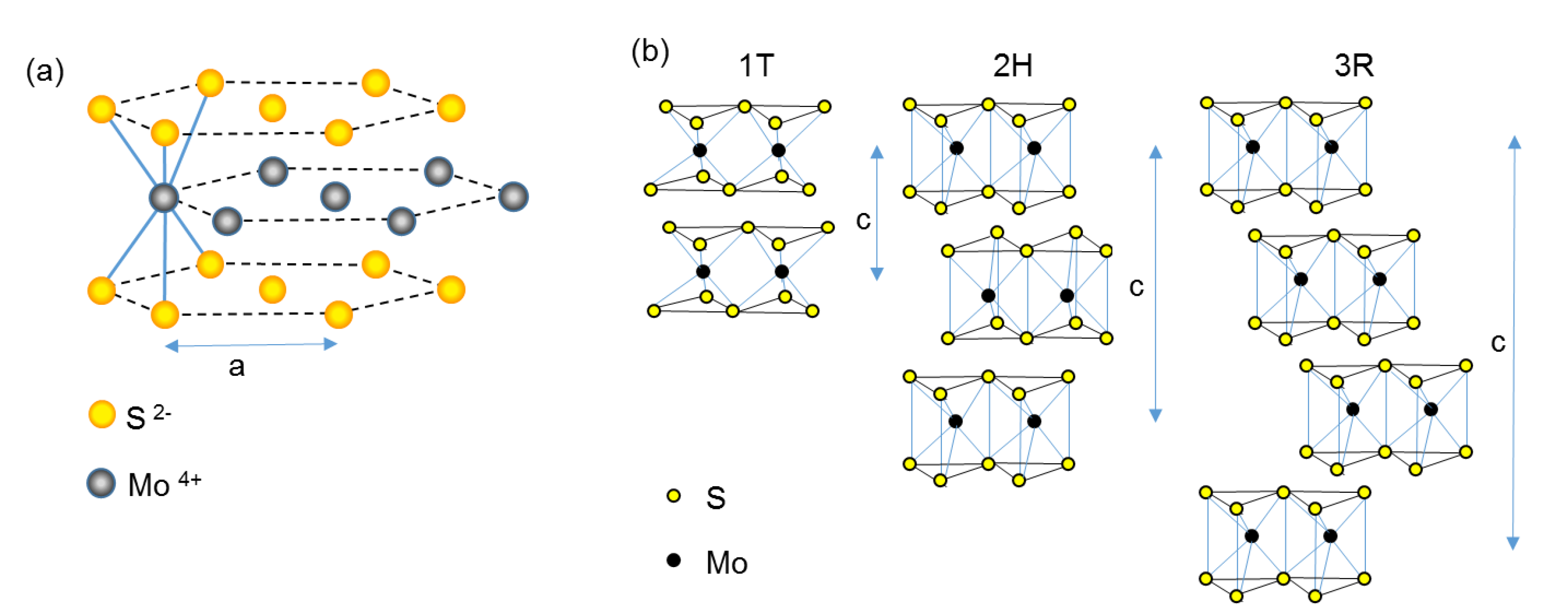
2. Crystal Structure

Molybdenum Disulfide (MoS2) belongs to a class of TMDC materials with a formula MX2, where M is a transition metal element of group IV (Ti, Zr, Hf), group V (V, Nb, Ta), or group VI (Mo, W), and X is a chalcogen (S, Se, Te). These materials form layered structures of the form X–M–X, with the chalcogen atoms in two hexagonal planes separated by a plane of transition metal atoms. For example, MoS2 has a layered structure of covalently bonded S–Mo–S, which is bonded to adjacent layers by weak van der Waals (vdW) interactions between neighboring S–S layers. As shown in Figure 2a, the S and Mo atom layers are hexagonal in structure and each Mo atom is located at the center of a trigonal prism created by six S atoms [19]. Such a tri-layer sandwich structure is considered as a monolayer of MoS2, and is stacked in three possible configurations, with weak vdW S–S bonds as shown in Figure 2b, to form multilayer MoS2.
Figure 2. (a) Hexagonal structure of S and Mo layers; (b) Side view schematic illustration of the 1T/2H/3R type structures of MoS2; (c) indicates the number of layers in a repeat unit.
Photonics 02 00288 g002
These vdW interactions allow MoS2 to form a bulk crystal of different polytypes, which vary by stacking order and atom coordination. As shown in Figure 2b, there are three known common MoS2 structures. The 2H and 3R structures both occur in nature, and have trigonal prismatic coordination [20]. The 3R type has rhombohedra symmetry with three S-Mo-S units. The 2H-MoS2 has hexagonal symmetry with two S–Mo–S units per primitive cell. The 1T type is a metastable structure discovered in the 1990s [21,22]. It has octahedral coordination with tetragonal symmetry. It has only one S–Mo–S as a repeat cell. Both the 1T and 3R types are metastable, and they can change to the 2H-MoS2 structure through heating [23,24]. All of the bulk MoS2 crystals discussed hereafter are of the 2H-MoS2 structure.

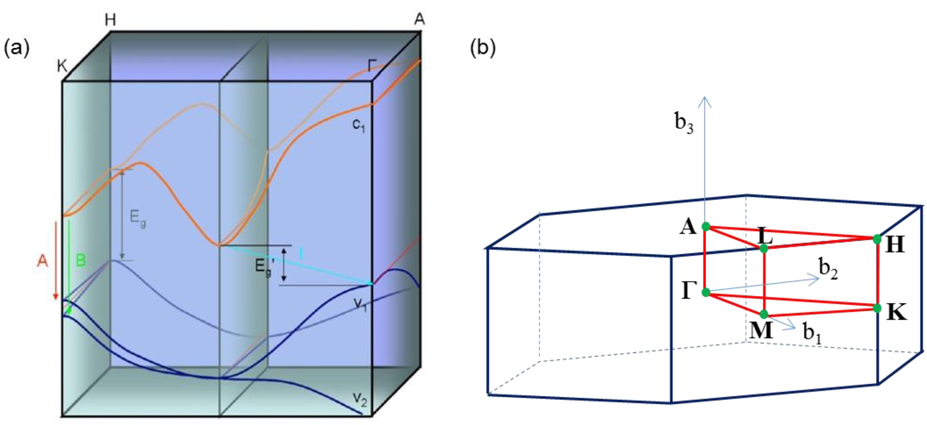
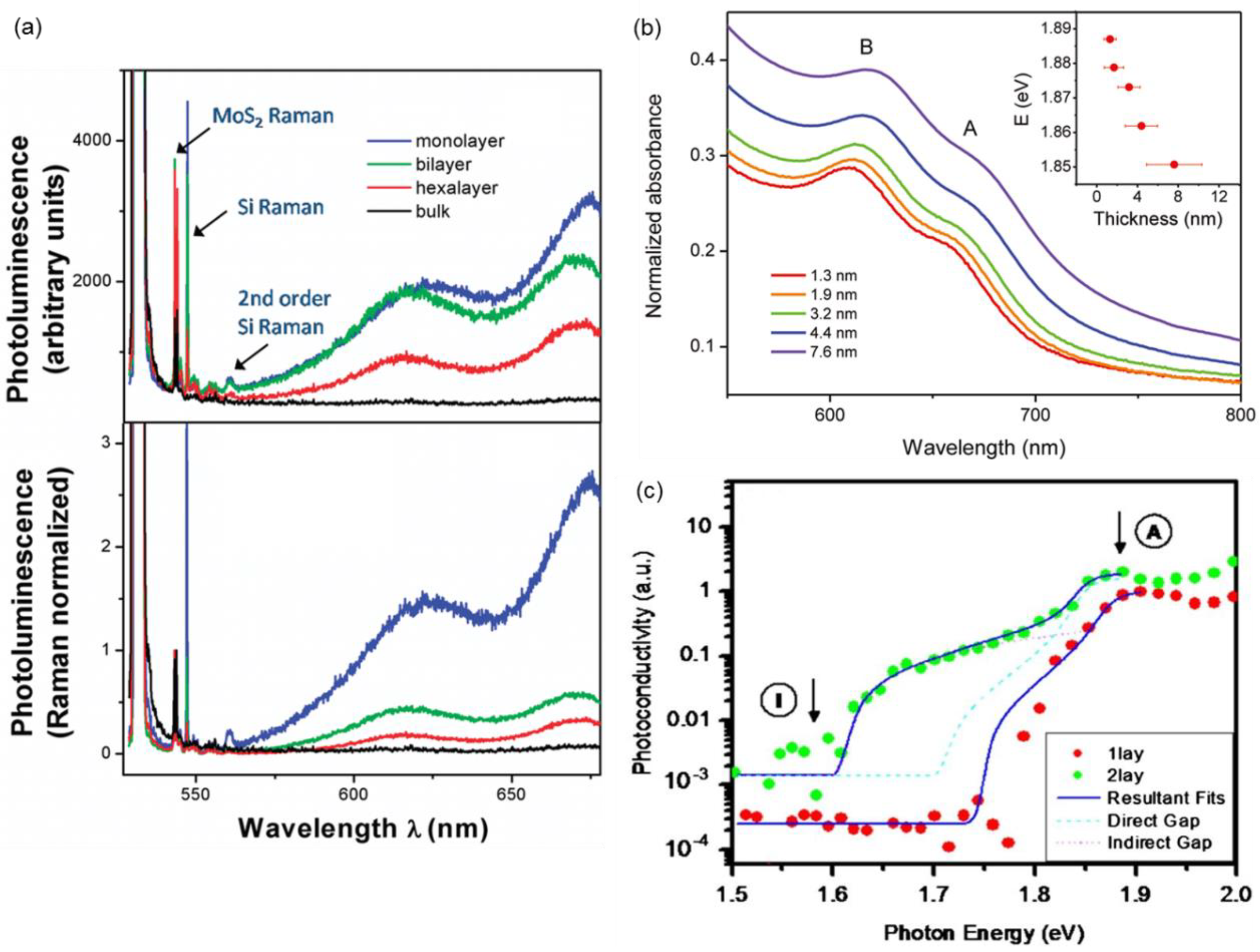
3. Electronic Band Structure: Optical and Optoelectronic Properties
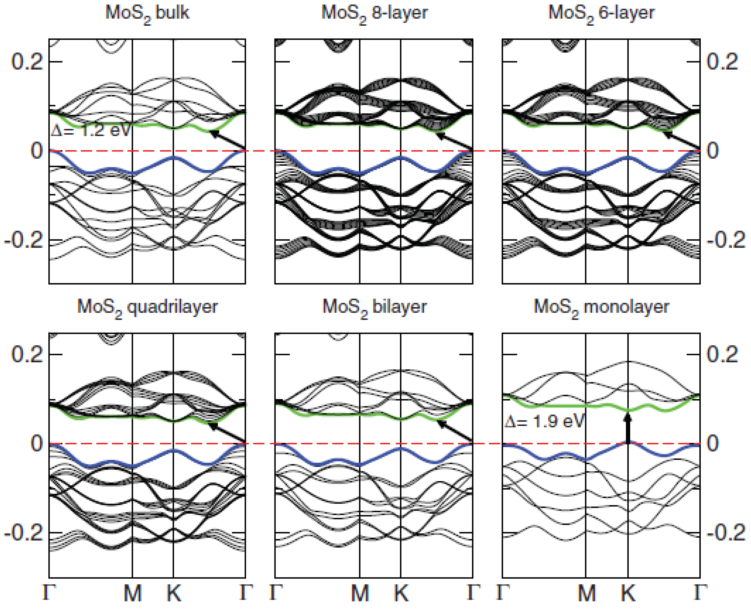
The electronic characteristics of TMDCs range from metal to semiconductor [14,15,25,26,27]. Many TMDCs’ electronic band structures have been theoretically investigated through the use of several modeling techniques. In the 1970s, semi-empirical calculations based on the tight-binding method were made by Bromley, Murray, and Yoffe without taking into account interlayer interaction effects [28,29]. From the 1970s to the present, ab initio and first principles calculations using density functional theory (DFT) with different approximations (e.g., local density approximations (LDA)) were made and widely used [30,31,32,33,34,35,36,37,38,39,40]. These models were guided by a variety of spectroscopic tools [14,18,24,27,41,42,43,44,45,46,47,48,49,50].
Figure 3. Band structure of different layers of MoS2 [36]. Reprinted figure with permission from [Kuc, A.; Zibouche, N.; et al. Influence of quantum confinement on the electronic structure of the transition metal sulfide TS2. Phys. Rev. B 2011, 83, 245213] Copyright (2011) by the American Physical Society.
Photonics 02 00288 g003
Recently, MoS2 has been of particular interest. As shown in Figure 3, bulk MoS2 is an indirect band gap semiconductor with a band gap of 1.2 eV, which originates from the top of the valence band situated at the Γ point to the bottom of the conduction band halfway between the Γ and K points. It should be noted that there is a direct band gap situated at the bulk MoS2 K point. As the number of layers decreases, the fundamental indirect band-gap (from the Γ point to halfway between the Γ point and the K point) increases due to the quantum confinement effect. In the case of monolayer MoS2, it becomes larger than the direct band-gap located at the K-point, which has been changed by less than 0.1 eV as the number of layers was reduced. In the monolayer limit, MoS2 changes from a bulk indirect band-gap semiconductor to a 2D direct band-gap semiconductor. The indirect band-gap of bulk MoS2 (1.2 eV) is supplanted by the direct band-gap (1.9 eV) at the monolayer MoS2 K-point, as shown in Figure 3.
This layer number-dependent band-structure is due to quantum confinement in the c-axis of the crystal. The band-gap change with film thickness was predicted by Sandomirskii in 1963; the band-gap of semiconducting films was shown to change by Δ E g = 2 π 2 2 m a 2 , where a is the film thickness [51,52]. Quantum confinement of carriers was also studied in ultrathin film MoS2 and other TMDCs [53,54,55]. The out-of-plane effective mass for electrons and holes around the K point is far exceeded by the free electron and hole mass (m0). Whereas the hole effective mass around the Γ point is estimated to be 0.4 m0, and the electron effective mass of the conduction band minimum along the Γ-K direction is only 0.6m0 [46]. Therefore, the decrease of thickness to monolayer leads to significant quantum confinement. To explain this result, Mak et al. applied a zone-folding scheme to describe the electronic band structure of ultrathin MoS2 film [46]. As shown in Figure 4a, the allowed electronic state’s wave vector (out-of-plane momentum k) for monolayer MoS2 can directly occur in the A-H direction. By increasing the MoS2 thickness, the out-of-plane momentum k will approach the Γ-K direction (Figure 4b). In this case the top of the conduction band and the bottom of the valence band occur at the Γ point and along the Γ-K direction. The d orbitals’ contribution to the band structure of MoS2 has been of particular research interest [25,28,32,33,42,56]. The 2H-MoS2 with trigonal prismatic coordination has a filled d z 2 valence band that overlaps the filled sp orbitals of the S atoms. The conduction band is derived from the degenerate d x 2 y 2 and d x orbitals that overlap the empty anti-bonding sp orbitals of the S atoms. Based on density of state (DOS) data [34,35,36,37,39], the valence and conduction bands near the Γ point were found to be a linear combination of d orbitals of the Mo atoms and pz orbitals of the S atoms. At the K point, the valence and conduction band states are primarily composed of the d orbitals of the Mo atoms, which are located in the middle of the S–Mo–S unit. Compared to the Mo atoms, the S atoms have strong interlayer coupling; their electron state energy depends on layer thickness, and leads to a direct band-gap structure at the K point when the layer thickness decreases.
Figure 4. (a) Simplified electronic band structure of bulk MoS2 [46]. Reprinted figure with permission from [Mak, K.F.; Lee, C.; James, H.; Jie, S.; Heinz, T.F. Atomically Thin MoS2: A New Direct-Gap Semiconductor. Phys. Rev. Lett. 2010, Phys. Rev. Lett. 105.136805] Copyright (2010) by the American Physical Society. (b) Brillouin zone and special point of the hexagonal lattice system (MoS2) [57].
Photonics 02 00288 g004
This and other layer-dependent band structure variation in TMDCs has recently seen increased research interest, particularly their optical and optoelectronic properties. For instance, as a result of the direct band-gap, photons with energy greater than the band-gap can be easily absorbed. Hence there is an obvious change in the photoluminescence, absorption, and photoconductivity spectra for ultrathin film MoS2, especially for monolayer MoS2 [24,46,47,49], as shown in Figure 5. This phenomenon allows the possibility of using MoS2 for optoelectronic applications [58].
As shown in Figure 5a, the photoluminescence peaks between 600 nm and 700 nm become stronger with the reduction in the number of layer of MoS2. The corresponding absorption peaks can be identified as shown in Figure 5b. Both of them correspond to A and B exciton transitions in the direct band-gap structure [14,18,59]. A clear indirect to direct band structure transition between bilayer and monolayer MoS2 can be best seen from the photocurrent spectra shown in Figure 5c. The direct band-gap energies of EA and EB, as measured by different methods, are summarized in Table 1. Initially, the research was in agreement that the A and B exciton transitions occur at the Γ point [60,61,62]. There was some disagreement from M. R. Khan and G. J. Goldsmith’s work in 1983, which put the A and B exciton transition at the A point of the Brillouin Zone [63]. However, further calculations have shown that the A and B exciton transitions at the K point [30,32,64,65,66]. The A and B exciton energy difference is due to the d–d transitions from the filled dx orbital to the degenerated dxy and dx2-y2 orbitals, which split by spin-orbit coupling [62,67].
Figure 5. (a) Photoluminescence spectra from monolayer to bulk MoS2 [47]. Reprinted figure with permission from [Splendiani, A.; Sun, L.; Zhang, Y.; Li, T.; Kim, J.; Chim, C.-Y.; Galli, G.; Wang, F. Emerging photoluminescence in monolayer MoS2. Nano Lett. 2010, 10, 1271–1275] Copyright (2010) by the American Chemical Society. (b) Absorption spectra of ultrathin film MoS2 from 1.3 nm to 7.6 nm. Inset figure shows the A exciton energy with film thickness [24]. Reprinted figure with permission from [Eda, G.; Yamaguchi, H.; Voiry, D.; Fujita, T.; Chen, M.; Chhowalla, M. Photoluminescence from chemically exfoliated MoS2. Nano Lett. 2011, 11, 5111–5116.] Copyright (2011) by the American Chemical Society. (c) Photoconductivity spectra of monolayer and bilayer MoS2 [46]. Reprinted figure with permission from [Mak, K.F.; Lee, C.; James, H.; Jie, S.; Heinz, T.F. Atomically Thin MoS2: A New Direct-Gap Semiconductor. Phys. Rev. Lett. 2010, Phys. Rev. Lett. 105.136805] Copyright (2010) by the American Physical Society.
Photonics 02 00288 g005
As a 2D material, monolayer MoS2 is expected to have strong excitonic effects, which will affect the optical properties. One of the commonly used calculation methods is the GW plus Bethe–Salpeter equation (GW-BSE), which computes quasiparticle band structure and optical response, including electron–electron/hole interactions. Although the previously reported experimental and theoretical band gap for MoS2 is around 1.9 eV, recent calculations based on the GW method for monolayer MoS2 have shown that the quasiparticle band-gap is larger. However, the calculated results vary widely between 2.2 and 2.8 eV [37,66,68,69,70,71,72]. Currently there is no experimental proof for the larger quasiparticle band-gap in MoS2, although evidence was recently demonstrated for WS2 [73].
Table 1. There is a wide range of published values of direct band-gap energy EA1 and EB1 measured at different temperatures.
Materials / MethodEA1 (eV)EB1 (eV)Temperature (K)
2H-MoS2 /piezo reflectance [74]1.929 ± 0.0052.136 ±.00825
1.845 ± 0.0082.053 ± 0.01300
2H-MoS2 / reflectance [14,75,76]1.882.06300
2H-MoS2 / wavelength modulation reflectance (WMR) [77]1.92552.1374.2
2H-MoS2 / photoconductivity [77]1.922.1244.2
2H-MoS2 / absorption [78]1.94492.13767
2H-MoS2 / absorption [44]1.902.10150
2H-MoS2 / absorption [44]1.912.1175/25
Inorganic Fullerene like 2H-MoS2 / absorption [79]1.821.95Room
2H-MoS2 / Bethe–Slapeter Equation (BSE) Calculation [66]1.781.96-
Monolayer MoS2 / absorption [46]1.882.03Room
Ultrathin-MoS2 / photoluminescence [47]1.851.98Room

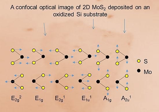
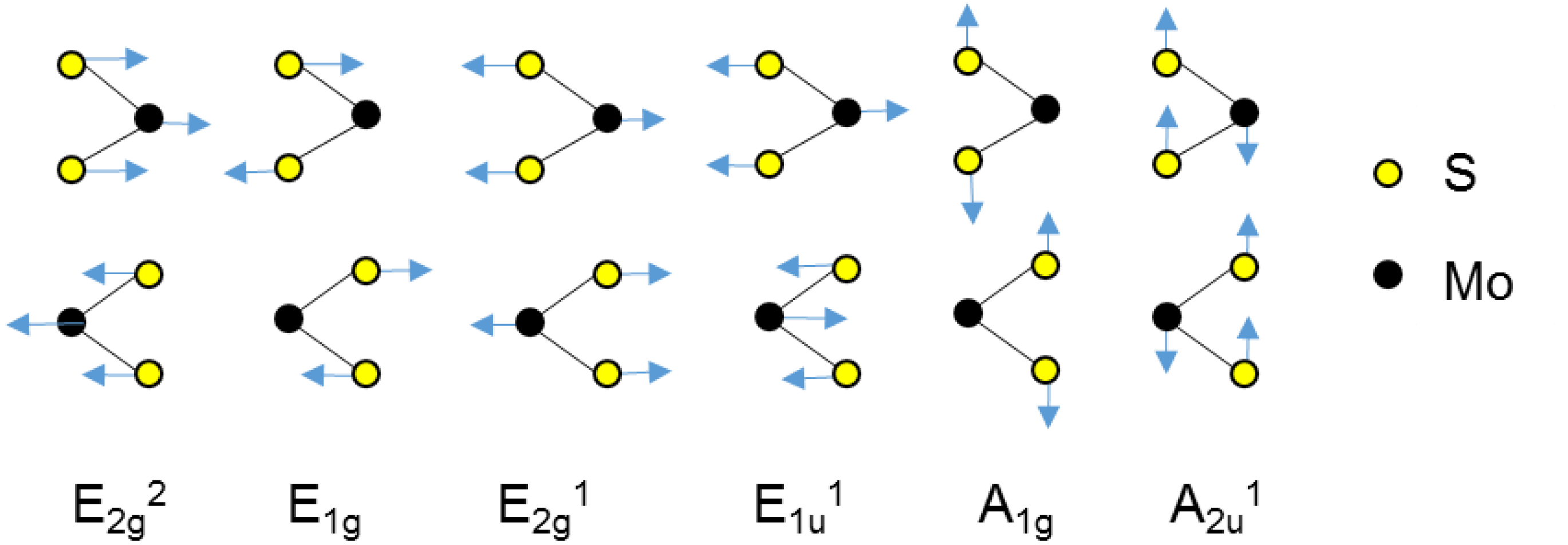
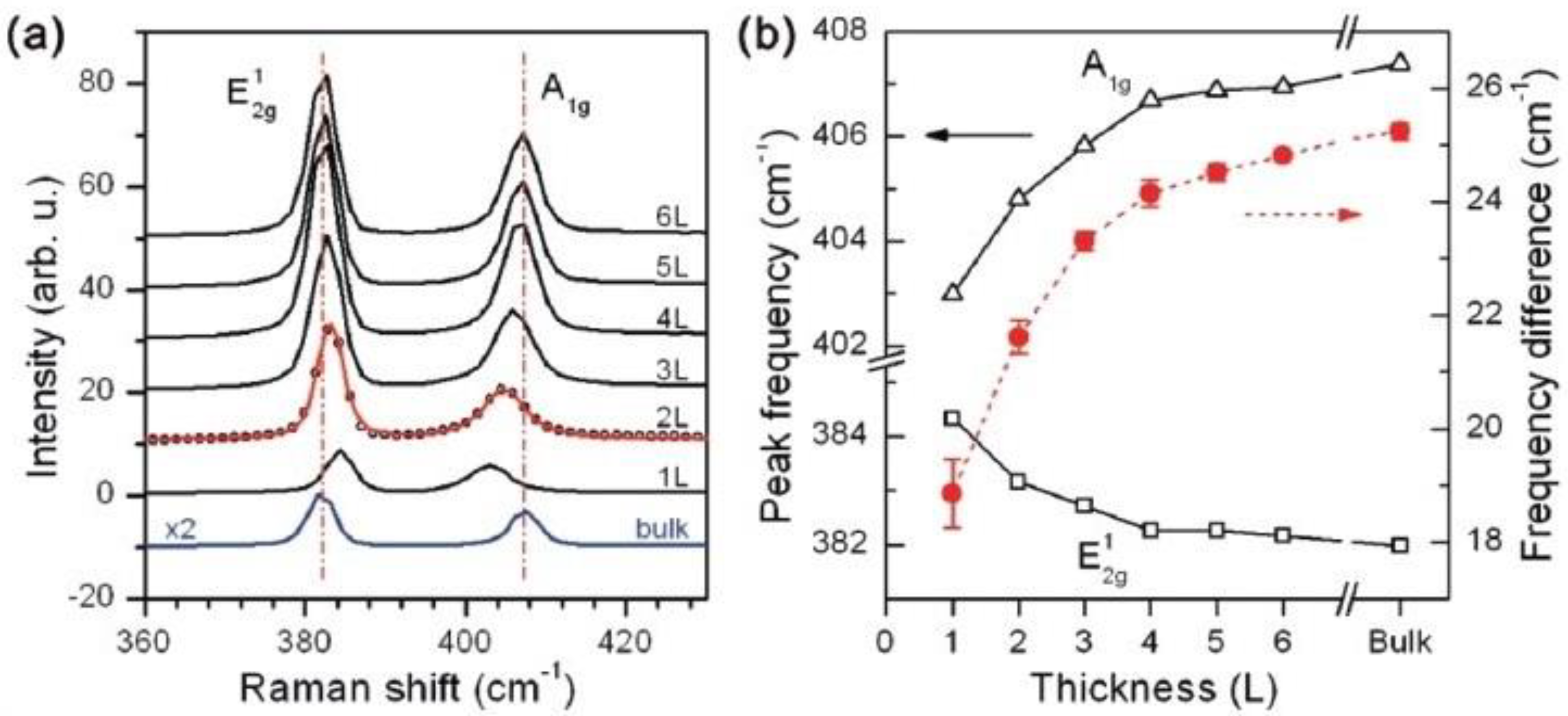
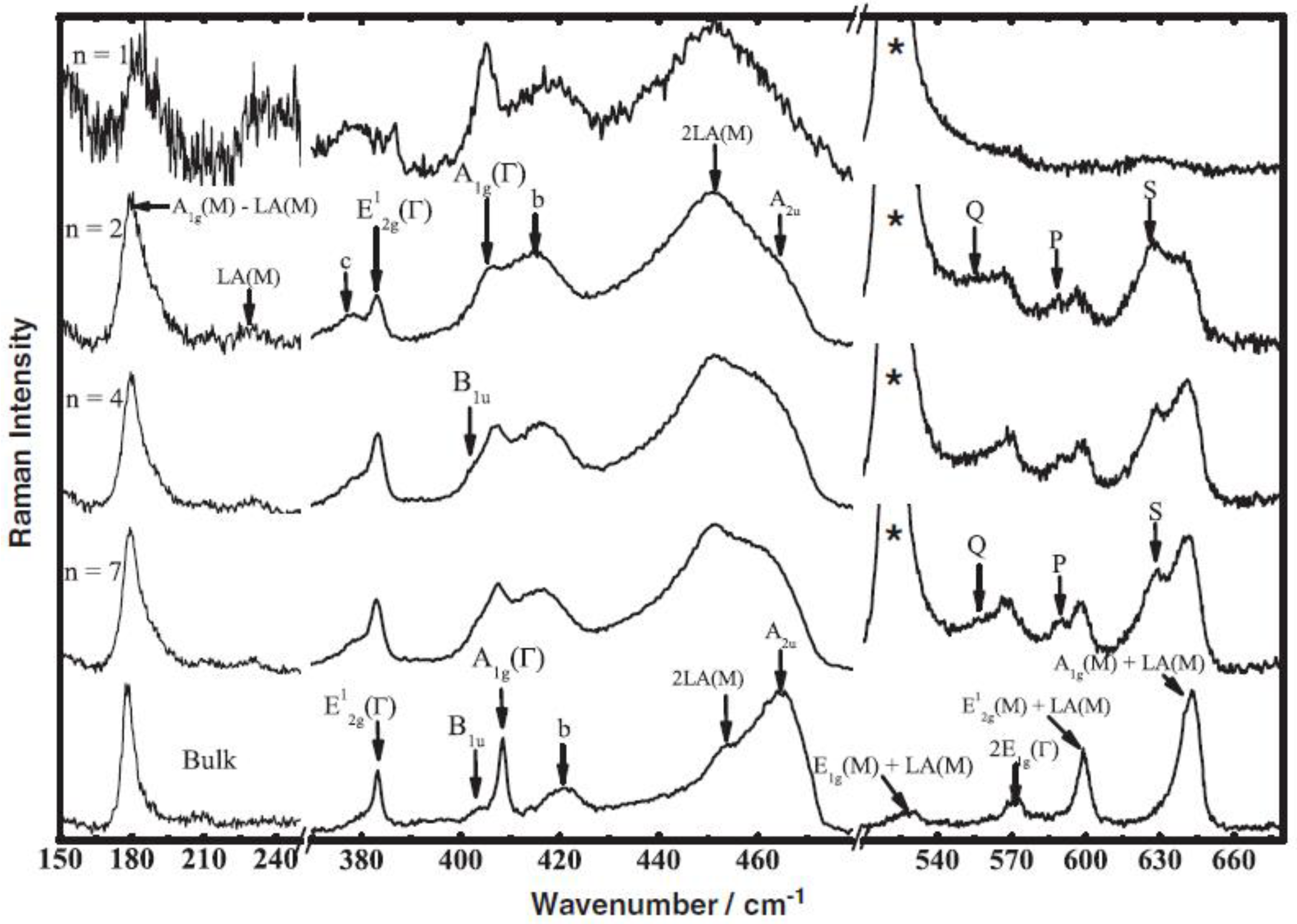
4. Lattice Dynamic: Raman Scattering and IR Absorption

Next we consider the lattice dynamics (Figure 6) in MoS2 that correspond to the phonon modes that contribute to Raman scattering and IR absorption. As was illustrated in Figure 2, MoS2 consists of two hexagonal planes of S atoms and an intercalated hexagonal plane of Mo atoms. The symmetry point group of the S atoms is C3v, while the symmetry of the Mo atoms is point group D3h. Furthermore, the irreducible representations of C3v and D3h are related to factor group D6h [80]. Therefore, MoS2 with even numbers of layers or bulk crystal have a symmetry similar to the D6h point group, and systems with odd numbers of layers (including monolayer crystals) have D3h space group symmetry (without inversion symmetry) [38].
Figure 6. Atomic displacement vector of the four first-order Raman-active E2g2, E1g, E2g1, A1g modes and two IR-active E1u1 and A2u1 modes, as viewed along the [100] direction [81,82,83].
Photonics 02 00288 g006
As shown in Table 2, there are four first-order Raman active modes that are present in most reported MoS2 Raman spectroscopy studies, A1g, E2g1, E2g2, and E1g. As shown in Figure 6, the A1g mode is due to the out-of-plane vibration among the S atoms as viewed along the [100] direction. The other three Raman active modes are due to in-plane vibrations, illustrated in Figure 6. Among the four Raman-active modes the A1g and E2g1 modes near 400 cm−1 are readily observable. The E1g mode and E2g2 mode usually cannot be detected by conventional Raman Scattering measurements.
Table 2. Relevant phonon irreducible symmetry representations of S atoms (C3v), Mo atoms (D3h), and bulk 2H-MoS2 point group D6h. This table is compiled from the work of T. J. Weiting et al. [80], A.M. Sanchez et al. [38], and T. Livneh et al. [84]. Some vibration frequency data were measured by [85,86].
C3v(S)D3h(Mo)D6h(MoS2(Γ))Transformation PropertiesActivityVibration DirectionAtoms InvolvedFrequency(cm−1)
A1A1A1gxx + αyyzz)RamanOutS409
A2B1u-InactiveOutS403
A2A1’’B2g1-InactiveOutMo + S475
B2g2-InactiveOutMo + S56
A2’’A2u1TzIR(E) c OutMo + S470
A2u2TzAcousticOutMo + S-
EE’E2g1xx - αyyzz)RamanInMo + S383
E1u1(Tx,Ty)IR(E) c InMo + S384
E2g2xx - αyyzz)RamanInMo + S34
E1u2(Tx,Ty)AcousticInMo + S-
E’’E1gyzzx)RamanInS286
E2u-InactiveInS297
The weak intensity of the E1g mode is due to the laser polarization chosen and random crystal direction of different MoS2 samples [86]. For example, the E1g mode is forbidden for s-polarized laser light incident on the MoS2 crystal surface (the E field is perpendicular to the c-axis of MoS2) [85]. In 1970, J. L. Verbel and T. J. Wieting studied the E1g mode, and predicted that it would be located around 519 cm−1 [83]. However, after correcting for the polarization effect in 1971 they discovered the very weak line at 287 cm−1 [80]. This was confirmed by J. M. Chen and C. S. Wang using back scattering geometry [87,88], which placed the E1g mode at 286 cm−1. This E1g mode has been shown to be more intense than the other three first-order Raman active modes, which are activated with the use of a p-polarized laser. Conversely, the E1g mode intensity is much weaker with the use of an s-polarized laser [85].
As shown in Figure 6, the E2g2 mode is due to the vibrational interaction of adjacent rigid layers within the MoS2 crystal. For this reason it is difficult to observe the E2g2 peak at low wavenumber, because of the presence of strong Rayleigh scattering. The corresponding Raman scattering peak for the E2g2 mode is located at 33.7( ± 1) cm−1 and was first experimentally observed by J. L. Verbel, T. J. Wieting, and P. R. Reed by use of a triple Raman spectrometer [89].
In addition to the four first-order Raman active modes (A1g, E2g1, E2g2, and E1g) there are four degeneracy lattice modes—E2u, E1u1, B1u, and B2g2—that are Raman inactive. Among these, E1u1 and A2u1 are IR active modes [83].
Figure 7. (a) Raman spectrum for different thicknesses of MoS2. (b) Frequencies of A1g and E2g1 modes against layer thickness [82]. Reprinted figure with permission from [Lee, C.; Yan, H.; Brus, L.E.; Heinz, T.F.; Hone, J.; Ryu, S. Anomalous lattice vibrations of single- and few-layer MoS2. ACS Nano 2010, 4, 2695–2700] Copyright (2010) by the American Chemical Society.
Photonics 02 00288 g007
It should be noted that most Raman spectra show strong signals for both the E2g1 and A1g modes, as shown in Figure 7a. To explain the vibrational modes of E2g1 and A1g, many classical models have been introduced. For example, Bromley used a Born–Von model in the nearest neighbor approximation in an attempt to explain this observation [90]. On the other hand, T. J. Wieting and J. L. Verble found that the classical dielectric oscillator model fits well with the infrared reflectivity and Raman scattering data [80]. This model fits well because the interlayer force is about 100 times smaller than the intralayer force [89], and therefore one only needs to consider the interatomic forces within a single layer. Furthermore, because of the small effective charge, the coulomb force is negligible [80]. However, C. Lee et al. found that these two modes exhibited abnormal film thickness dependence, as shown in Figure 7 [81]. For instance, as shown in Figure 7b, when the film thickness is increased the frequency of the E2g1 mode decreases (red shifts) while the A1g increases (blue shifts). This width-dependent frequency shift means that the E2g1 and A1g frequency are better for identifying ultrathin MoS2 thickness than either peak intensity or width for no more than four layers [91]. This result is consistent with optical microscope, atomic force microscopy (AFM), and photoluminescence measurements [47,81,91]. Based on various published sources, we have summarized in Table 3 the E2g1 and A1g mode frequencies detected from bulk and thin layers of MoS2 by various laser wavelengths.
The dependence of the E2g1 and A1g modes’ frequency on the layer thickness of MoS2 can be explained using the van der Waals force model. As the number of layers is increased, the restoring force between inter-layer S–S bonds will enhance, which fits the observed trend of the out-of-plane A1g mode frequency increasing. However, the E2g1 peak shows a red-shift as the number of layers is increased, which suggests that the classical model for coupled harmonic oscillators is inadequate and there is an additional interlayer interaction. One reason for the inadequacy of the classical model is that it only considers weak interlayer interaction. However, the properties of the MoS2 layers might be different from those on the surface of bulk MoS2. This is consistent with surface phenomenon measurements investigated by P. A. Bertrand, who reported the surface phonon dispersion of MoS2 as measured by high resolution electron-energy-loss spectroscopy (HREELS). It was found that the peak energy of the A1g optical mode for thin layers is 3.1( ± 0.2) meV lower than the related bulk phonon [92].
Table 3. Summary of the E2g1 and A1g mode frequency of MoS2 as excited by different laser sources and varied by the number of layers [91]. The 514.5# nm data is extracted from C. Lee et al. [82]. The 514.5 nm* and 632.8 nm* data only have 1/2/4/7/bulk layers [93].
Laser (nm)E2g1 Mode Frequency (cm−1) A1g Mode Frequency (cm−1)
1 L2 L3 L4 Lbulk1 L2 L3 L4 Lbulk
325384.2382.8382.8382.7382.5 404.9405.5406.3407407.8
488384.7383.3383.2382.9383 402.8405.5406.5407.4408
514.5#384.3383.2382.7382.3382 403404.8405.8406.7407.8
514.5*386.1383.1-383.7383.3 404.7406.8-408408.6
532384.7382.5382.4382.4383 402.7404.9405.7406.7407.8
632.8385383.8383.3382.9381.5 403.8404.8405406406.6
632.8*386.4383.1-383.3382.8 405406.2-407.3408.3
In fact, the red shift of the E2g1 peak with the increase in layer thickness is due to the fact that thinner MoS2 has a shorter intra-layer S–Mo–S distance. In 1977, B. J. Mrstik et al. found surface reconstruction in MoS2 by the use of low-energy electron diffraction (LEED). These LEED measurements showed that the topmost intra-layer space between S–Mo–S atoms of thin MoS2 contracts up to 5% compared to that in bulk planes [94]. These results show that layer stacking effects change the intralayer structure. Moreover, A. M. Sanchez and L. Wertz introduced long-range Coulomb interlayer interactions into models of multilayer MoS2 to explain the E2g1 anomalous red-shift when the thickness is increased [38]. It was previously introduced to explain the vibrational mode of β-GaSe by T. J. Wieting et al. [95]. From these models it is apparent that the interlayer force changes in two ways when moving from monolayer to bulk samples. The short-range term of the force slightly increases because of the enhanced restoring interaction between adjacent layers. The long-range term of the force will decrease, because the layers extend over the effective charge, which leads to Coulombic screening [96]. However, this effect mainly happens between the Mo atoms. From Figure 6 the E2g1 mode involves the in-plane vibration of Mo atoms. Consequently, the considerable decrease in the Coulombic, long-range interaction between the Mo atoms overcompensates for the slight increase of the short-range weak interlayer interaction. On the other hand, the A1g mode is not influenced by the Coulomb potential screening, because the A1g mode only involves out-of-plane vibration of the S atoms.

5. Resonant Raman Scattering

Besides the four first-order Raman modes and their degeneracy modes, J. M. Chen and C. S. Wang have noted that additional second-order modes appear when an Argon 514.5 nm laser source is used [85]. Furthermore, they found that the A1g mode combines with a weak longitudinal acoustic phonon mode at the M point of the Brillouin zone (LA(M)) corroborating inelastic neutron scattering data from Wakabayashi et al. [97].
In 1984, A. M. Stacy and D. T. Hodul presented Raman Spectra of MoS2 using 676.4 nm (1.83 eV), 647.1 nm (1.92 eV), and 530.9 nm (2.34 eV) excitation lasers whose energy is either near or just out of the edge of the MoS2 absorption region [86]. Typically resonance Raman Scattering is excited by use of a He-Ne 632.8 nm (1.96 eV) laser whose energy is between two absorption bands A (~1.9 eV) and B (~2.1 eV), and falls in the region of electronic transition. The resonance Raman spectra show that multiple modes are shifted from the first-order Raman frequencies, which suggests that the electronic transitions are strongly coupled with phonon modes. There are several reports of this resonant Raman scattering phenomenon in MoS2 [78,79,86,91,93,98,99,100]. All of these studies are in general agreement on the attribution of the peaks observed in the resonant Raman scattering spectrum, which suggests coupling between vibrational modes and longitudinal acoustic phonon modes.
Table 4. The phonon frequency of Raman-active and LA modes at different points of the Brillouin zone.
Phonon Frequency (cm−1)
Γ[80,85,86]M[97]M[84]K[84]
A1g409397412408
E2g1383373370345
E1g287294330336
309
E2g234-233(LA)241(LA)
160(ZA)192(ZA)
LA-234235241
The resonant Raman spectra are mainly due to contributions from the second order Raman processes at the high symmetry Γ, M, and K points of the Brillouin zone. Inelastic neutron scattering data have shown that the energy dispersion of the E1g, E2g1, and A1g modes in the Γ-M (from center to the [100] plane (shown in Figure 4b)) direction is relatively small [97]. From the measurement of resonance Raman spectra in Table 4, the line of the A1g (M) mode almost corresponds to the calculated value of A1g (Γ) (409 cm−1) mode. Similarly, the estimated value of the E2g1 (M) mode is a little smaller than the calculated value of the E2g1 (Γ) (383 cm−1) mode, which is consistent with Coulombic force theory [38]. However, as shown in Table 4, the energy of the E2g2 rigid layer mode at the M points increases considerably in the Γ–M direction due to the aforementioned longitudinal acoustic mode LA (M) interaction [97]. The phonon dispersion has three acoustic modes, whose frequencies linearly depend on the wave-vector. They play an important role in the resonance Raman spectrum of MoS2. The longitudinal acoustic (LA), and transverse acoustic (TA) modes are due to in-plane vibration. They both have a linear dispersion and higher energy than the out-of-plane acoustic (ZA) mode [38]. The dispersion of the LA, TA, and ZA modes flatten at the border of the Brillouin zone near the high-symmetry M point. Even though it is hard to observe in bulk MoS2 as shown in Figure 8, this LA (M) mode has been observed in MoS2 nanoparticles [79], MoS2 monolayer [101], few layers [93], and their aqueous suspension [21]. Hence the peak at ~230 cm−1 is related to the structural defect-induced scattering in MoS2 [93]. Lack of this feature may confirm relatively good crystal quality for the natural MoS2 sample [102].
The profile of many of the first- and second-order peaks between 100 cm−1 and 700 cm−1 can be seen in Figure 8. One of the most pronounced peaks is the multi-modeband at 466 cm−1. Generally it is attributed to the 2LA (M) mode at ~450 cm−1 [78,79,86], and the normally IR-active A2u (Γ) phonon mode near 466 cm−1 [97]. In addition, K. Golasa et al. proposed a new phonon mode XA around 180 cm−1 [100]. They suggested that the high energy component of the 466 cm−1 peak is rather due to a combined mode E1g (M) + XA (M), even if the E1g is forbidden by back scattering geometry. Similarly, the E1g + LA (M) mode at 528 cm−1 has been observed in many different samples. Contrary to previous studies [79,86,91,93,101,103], which simply assign the peak at ~645 cm−1 as A1g (M) + LA (M), K. Golasa et al. [100,104] suggest it is composed of two components: the high-wavenumber part is due to the E1g + 2XA (M) modes and the low-wavenumber one, which is marked as “S” in Figure 8, is the real A1g (M) + LA (M) process. In this way, G. L. Frey’s description of the 641 cm−1 peak shift to low-energy in MoS2 nanoparticles can be explained [98].
There are multiple emergent modes around the two first-order Raman active modes E2g1 and A1g in Figure 8. Three additional bands marked “a,” “b,” and “c” are in the vicinity of the E2g1 and A1g peaks [78,93,98,100,104]. The “a” band is at ~395 cm−1, which is not shown in Figure 8 but has been observed by Sekine et al., Livneh et al., and Golasa et al. [78,98,104]. The mode labeled “b” at 420 cm−1 is attributed to a two-phonon Raman scattering process ω b = ω Q A + ω T O . It involves the successive emission of a dispersive longitudinal quasi-acoustic (QA) phonon and a dispersionless transverse optical (TO) phonon. The QA phonon belongs to the Δ2 branch along the c axis (ending in the B2g2 inactive mode at the Γ point). The TO phonon has a finite vector near the Γ point (with E2u1 symmetry) of the Δ6 branch along the c axis [97]. Using this, Livneh explains the ~5 cm−1 difference in the “b” mode between the Stokes and anti-Stokes Raman spectra [98]. Therefore, the band denoted as “c” at ~ 377 cm−1 corresponds to this TO phonon. However, unlike the IR spectrum result [80], the “c” band was directly considered to be the E1u2 mode in Sekine’s measurement [78]. P. N. Ghosh et al.’s calculation based on the vdW interlayer model also obtained E1u2 at 2 cm−1 lower than the E2g1 mode [105], but they suggest the probability of long-range Coulombic interaction. Finally, A. M. Sanchez et al. made ab initio calculations considering long-range Coulombic interaction, which showed that the E1u2 mode is 3 cm−1 higher than E2g1 mode [38]. The IR-active mode E1u2 can be experimentally observed at the high wavenumber side of the E2g1 mode from the resonant Raman scattering in Livneh’s work [98]. Another Raman-inactive mode, B1u, which is the Davydov pair of A1g modes, is also observed at the low-wavenumber side of the A1g band [78,93,98].
Resonance Raman spectra taken on different MoS2 thicknesses from monolayer to bulk are shown in Figure 8. One of the most significant differences is that almost all the resonance peaks are broadened and the relative intensity change as a result of thickness decreases, as was previously reported [91]. The change in the shape and location of the resonance modes at ~ 465 cm−1 and 643 cm−1 have been explained in detail by K. Golasa et al. [100,104]. In addition, the resonance Raman modes higher than 500 cm−1 are hardly observed in the spectrum of monolayer MoS2. There are several possible reasons for this result. The most reasonable possibility is that the long-range acoustic modes in monolayer MoS2 are strongly affected by interactions with the substrate [99,104]. In the bulk case, only a relatively tiny amount of atoms in the whole sample directly interact with the substrate, and the substrate therefore has little impact on the lattice vibrations. Under resonance conditions, the modification of acoustic modes by the substrate causes the suppression of most multi-phonon processes.
Figure 8. Resonant Raman spectra of different thickness MoS2 using 632.8 nm laser in room temperature [93]. Reprinted figure with permission from [Chakraborty, B.; Matte, H.S.S.R.; Sood, A.K.; Rao, C.N.R. Layer-dependent resonant Raman scattering of a few layer MoS2. J. Raman Spectrosc. 2013, 44, 92–96.] Copyright (2013) by John Wiley and Sons.
Photonics 02 00288 g008
Another result of the resonant spectra is that mode “b” at ~420 cm−1 seems to still be present in monolayer MoS2 at room temperature [93,101,104]. However, there is no quasi-acoustical mode present in the monolayer limit, thus the behavior contradicts its assignment to the combined process involving the quasi-acoustic phonons. Therefore, mode “b” should not be present in the monolayer MoS2 spectrum at all. Based on the data from K. Golasa, the peak “b” at ~420 cm−1 clearly disappears from the spectrum in the monolayer MoS2 at 4.2 K. This observation also seems to suggest that a new model is needed to explain the apparent presence of the mode “b” at ~420 cm−1.
Finally, the intensity of resonance Raman modes have an observed temperature dependence in some studies [85,98,99,100,106]. For example, J. M. Chen and C. S. Wang had detected both the dependence of the second-order Raman modes at room temperature (300K) and liquid nitrogen temperature (80K). These resonance modes can be explained based on the following relations:
  • Difference process: I n ( 1 , T ) × [ n ( 2 , T ) + 1 ]
  • Combination process: I [ n ( 1 , T ) + 1 ] × [ n ( 2 , T ) + 1 ] ,
where n ( i , T ) = 1 e i / kT 1 is the phonon number related to temperature T for phonons with frequency ωi [85]. Based on these absorption and excitation processes for phonons, they tentatively identify two low frequency peaks at 150 cm−1 and 188 cm−1 and three high frequency peaks at 567 cm−1, 750 cm−1, and 816 cm−1.

6. Conclusions

The emergence of 2D materials has led to increased attention on correlating the structural, optical, and optoelectronic properties of thin MoS2 layers. Although these properties have been studied for bulk MoS2 since the 1960s, the discovery of graphene has led to more interest in the investigation of these properties for 2D thin films of MoS2. Since the discovery of the relationship between Raman and photoluminescence (PL) spectra with the film thickness of MoS2 in 2010, these optical spectra have become reliable and popular signals for the identification of mono- or few-layered MoS2 structures.

Acknowledgements

Yoke Khin Yap acknowledges the support from the National Science Foundation (Award number DMR-1261910).

Conflicts of Interest

The authors declare no conflict of interest.

References

  1. Novoselov, K.S.; Geim, A.K.; Morozov, S.V.; Jiang, D.; Zhang, Y.; Dubonos, S.V.; Grigorieva1, I.V.; Firsov, A.A. Electric field effect in atomically thin carbon films. Science 2004, 306, 666–669. [Google Scholar] [CrossRef] [PubMed]
  2. Novoselov, K.S.; Jiang, D.; Schedin, F.; Booth, T.J.; Khotkevich, V.V.; Morozov, S.V.; Geim, A.K. Two-dimensional atomic crystals. PNAS 2005, 102, 10451–10453. [Google Scholar] [CrossRef] [PubMed]
  3. Geim, A.K.; Grigorieva, I.V. Van der Waals heterostructures. Nature 2013, 499, 419–425. [Google Scholar] [CrossRef] [PubMed]
  4. Castro Neto, A.H.; Guinea, F.; Peres, N.M.R.; Novoselov, K.S.; Geim, A.K. The electronic properties of graphene. Rev. Mod. Phys. 2009, 81, 109–162. [Google Scholar] [CrossRef]
  5. Elias, D.C.; Gorbachev, R.V.; Mayorov, A.S.; Morozov, S.V.; Zhukov, A.A.; Blake, P.; Ponomarenko, L.A.; Grigorieva, I.V.; Novoselov, K.S.; Guinea, F.; et al. Dirac cones reshaped by interaction effects in suspended graphene. Nat. Phys. 2011, 7, 701–704. [Google Scholar]
  6. Chen, H.; Müller, M.B.; Gilmore, K.J.; Wallace, G.G.; Li, D. Mechanically Strong, Electrically Conductive, and Biocompatible Graphene Paper. Adv. Mater. 2008, 20, 3557–3561. [Google Scholar]
  7. Lin, M.W.; Ling, C.; Zhang, Y.; Yoon, H.J.; Cheng, M.M.-C.; Agapito, L.A.; Kioussis, N.; Widjaja, N.; Zhou, Z. Room-temperature high on/off ratio in suspended graphene nanoribbon field-effect transistors. Nanotechnology 2011, 22, 265201. [Google Scholar] [CrossRef] [PubMed]
  8. Song, L.; Ci, L.J.; Lu, H.; Sorokin, P.B.; Jin, C.; Ni, J.; Kvashnin, A.G.; Kvashnin, D.G.; Lou, J.; Yakobson, B.I.; Ajayan, P.M. Large Scale Growth and Characterization of Atomic Hexagonal Boron Nitride Layers. Nano Lett. 2010, 10, 3209–3215. [Google Scholar] [CrossRef] [PubMed]
  9. Kim, K.K.; Hsu, A.; Jia, X.; Kim, S.M.; Shi, Y.; Hofmann, M.; Nezich, D.; Rodriguez-Nieva, J.F.; Dresselhaus, M.; et al. Synthesis of Monolayer Hexagonal Boron Nitride on Cu Foil Using Chemical Vapor Deposition. Nano Lett. 2012, 12, 161–166. [Google Scholar] [CrossRef] [PubMed]
  10. Lee, C.H.; Qin, S.Y.; Savaikar, M.A.; Wang, J.; Hao, B.; Zhang, D.; Banyai, D.; Jaszczak, J.A.; Clark, K.W.; et al. Room-Temperature Tunneling Behavior of Boron Nitride Nanotubes Functionalized with Gold Quantum Dots. Adv. Mater. 2013, 25, 4544–4548. [Google Scholar] [CrossRef] [PubMed]
  11. Lee, C.H.; Xie, M.; Kayastha, V.; Wang, J.; Yap, Y.K. Patterned Growth of Boron Nitride Nanotubes by Catalytic Chemical Vapor Deposition. Chem. Mater. 2010, 22, 1782–1787. [Google Scholar] [CrossRef]
  12. Wang, J.S.; Lee, C.H.; Yap, Y.K. Recent advancements in boron nitride nanotubes. Nanoscale 2010, 2, 2028–2034. [Google Scholar] [CrossRef] [PubMed]
  13. Wang, J.S.; Kayastha, V.K.; Yap, Y.K.; Fan, Z.; Lu, J.G.; Pan, Z.; Ivanov, I.N.; Puretzky, A.A.; Geohegan, D.B. Low temperature growth of boron nitride nanotubes on substrates. Nano Lett. 2005, 5, 2528–2532. [Google Scholar] [CrossRef] [PubMed]
  14. Wilson, J.A.; Yoffe, A.D. The transition metal dichalcogenides discussion and interpretation of the observed optical, electrical and structural properties. Adv. Phys. 1969, 18, 193–335. [Google Scholar] [CrossRef]
  15. Yoffe, A.D. Layer compounds. Annu. Rev. Mater. Sci. 1973, 3, 147–170. [Google Scholar] [CrossRef]
  16. Radisavljevic, B.; Radenovic, A.; Brivio, J.; Giacometti, V.; Kis, A. Single-layer MoS2 transistors. Nat. Nanotech. 2011, 6, 147–150. [Google Scholar] [CrossRef]
  17. Yoon, Y.; Ganapathi, K.; Salahuddin, S. How good can monolayer MoS2 transistors be? Nano Lett. 2011, 11, 3768–3773. [Google Scholar] [CrossRef] [PubMed]
  18. Frindt, R.F.; Yoffe, A.D. Physical Properties of Layer Structures: Optical Properties and Photoconductivity of Thin Crystals of Molybdenum Disulphide. Proceedings A 1963, 27369–27383. [Google Scholar]
  19. Dickinson, R.G.; Pauling, L. The crystal structure of molybdenite. J. Am. Chem. Soc. 1923, 45, 1466–1471. [Google Scholar]
  20. Jellinek, P.; Brauer, G.; Müller, H. Molybdenum and Niobium Sulphides. Nature 1960, 185, 185376–185377. [Google Scholar] [CrossRef]
  21. Jiménez Sandoval, S.; Yang, D.; Frindt, R.F.; Irwin, J.C. Raman study and lattice dynamics of single molecular layers of MoS2. Phys. Rev. B 1991, 44, 3955–3962. [Google Scholar] [CrossRef]
  22. Wypych, F.; Schollhorn, R. 1T-Mos2, a New Metallic Modification of Molybdenum-Disulfide. J. Chem. Soc. -Chem. Commun. 1992, 19, 1386–1388. [Google Scholar] [CrossRef]
  23. Enyashin, A.N.; Yadgarov, L.; Houben, L.; Popov, I.; Weidenbach, M.; Tenne, R.; Bar-Sadan, M.; Seifert, G. New Route for Stabilization of 1T-WS2 and MoS2 Phases. J. Phys. Chem. C 2011, 115, 24586–24591. [Google Scholar] [CrossRef]
  24. Eda, G.; Yamaguchi, H.; Voiry, D.; Fujita, T.; Chen, M.; Chhowalla, M. Photoluminescence from chemically exfoliated MoS2. Nano Lett. 2011, 11, 5111–5116. [Google Scholar] [CrossRef] [PubMed]
  25. Mattheiss, L.F. Band Structures of Transition-Metal-Dichalcogenide Layer Compounds. Phys. Rev. B 1973, 8, 3719–3740. [Google Scholar] [CrossRef]
  26. Shepherd, F.R.; Williams, P.M. Photoemission studies of the band structures of transition metal dichalcogenides. I. Groups IVA and IVB. J. Phys. C: Solid State Phys. 1974, 4416, 74416–74426. [Google Scholar]
  27. Shepherd, F.R.; Williams, P.M. Photoemission studies of the band structures of transition metal dichalcogenides. II. Groups VA and VIA. J. Phys. C: Solid State Phys. 1974, 4427, 74427–74439. [Google Scholar]
  28. Bromley, R.A.; Murray, R.B.; Yoffe, A.D. The band structures of some transition metal dichalcogenides. III. Group VIA trigonal prism materials. J. Phys. C: Solid State Phys. 1972. [Google Scholar] [CrossRef]
  29. Bromley, R.A. A Semi-Emprical Tight-Banding Calculation of the Band Structure of MoS2. Phys. Lett. 1970, 33, 33242–33243. [Google Scholar] [CrossRef]
  30. Mattheiss, L.F. Energy Bands for 2H-NbSe2 and 2H-MoS2. Phys. Rev. Lett. 1973, 30, 784–787. [Google Scholar] [CrossRef]
  31. Edmondson, D.R. Electronic band structure of the layer-type crystal 2H-MoS2. Solid State Commun. 1972, 10, 101085–101088. [Google Scholar] [CrossRef]
  32. Coehoorn, R.; Haas, C.; de Groot, R.A. Electronic structure of MoSe2, MoS2, and WSe2. II. The nature of the optical band gaps. Phys. Rev. B 1987, 35, 6203–6206. [Google Scholar]
  33. Reshak, A.H.; Auluck, S. Band structure and optical response of 2H-MoX2 compounds (X = S, Se, and Te). Phys. Rev. B 2005. [Google Scholar] [CrossRef]
  34. Li, T.S.; Galli, G.L. Electronic properties of MoS2 nanoparticles. J. Phys. Chem. C 2007, 111, 16192–16196. [Google Scholar] [CrossRef]
  35. Lebègue, S.; Eriksson, O. Electronic structure of two-dimensional crystals from ab initio theory. Phys. Rev. B 2009, 79, 115409. [Google Scholar] [CrossRef]
  36. Kuc, A.; Zibouche, N.; Heine, T. Influence of quantum confinement on the electronic structure of the transition metal sulfide TS2. Phys. Rev. B 2011, 83, 245213. [Google Scholar]
  37. Ding, Y.; Wang, Y.; Ni, J.; Shi, L.; Shi, S.; Tang, W. First principles study of structural, vibrational and electronic properties of graphene-like MX2 (M = Mo, Nb, W, Ta; X = S, Se, Te) monolayers. Phys. B: Condens. Matt. 2011, 406, 2254–2260. [Google Scholar] [CrossRef]
  38. Molina-Sánchez, A.; Wirtz, L. Phonons in single-layer and few-layer MoS2 and WS2. Phys. Rev. B 2011, 84, 155413. [Google Scholar] [CrossRef]
  39. Kadantsev, E.S.; Hawrylak, P. Electronic structure of a single MoS2 monolayer. Solid State Commun. 2012, 152, 909–913. [Google Scholar] [CrossRef]
  40. Yun, W.S.; Han, S.W.; Hong, S.C.; Kim, I.G.; Lee, J.D. Thickness and strain effects on electronic structures of transition metal dichalcogenides: 2H-MX2 semiconductors (M = Mo, W; X = S, Se, Te). Phys. Rev. B 2012. [Google Scholar] [CrossRef]
  41. Kam, K.K.; Parklnclon, B.A. Detailed Photocurrent Spectroscopy of the Semiconducting Grouping VI Transition Metal Dichalcogenides. J. Phys. Chem. 1982, 86, 86463–86467. [Google Scholar] [CrossRef]
  42. Coehoorn, R.; Haas, C.; Dijkstra, J.; Flipse, C.J.; de Groot, R.A.; Wold, A. Electronic structure of MoSe2, MoS2, and WSe2. I. Band-structure calculations and photoelectron spectroscopy. Phys. Rev. B 1987, 35, 6195–6202. [Google Scholar]
  43. Kobayashi, K.; Yamauchi, J. Electronic structure and scanning-tunneling-microscopy image of molybdenum dichalcogenide surfaces. Phys. Rev. B Condens. Matt. 1995, 51, 17085–17095. [Google Scholar] [CrossRef]
  44. Frey, G.L.; Elani, S.; Homyonfer, M.; Feldman, Y.; Tenne, R. Optical-absorption spectra of inorganic fullerenelike MS2 (M = Mo, W). Phys. Rev. B 1998. [Google Scholar] [CrossRef]
  45. Böker, T.; Severin, R.; Müller, A.; Janowitz, C.; Manzke, R.; Voß, D.; Krüger, P.; Mazur, A.; Pollmann, J. Band structure of MoS2, MoSe2, and α-MoTe2: Angle-resolved photoelectron spectroscopy and ab initio calculations. Phys. Rev. B 2001. [Google Scholar] [CrossRef]
  46. Mak, K.F.; Lee, C.; James, H.; Jie, S.; Heinz, T.F. Atomically Thin MoS2: A New Direct-Gap Semiconductor. Phys. Rev. Lett. 2010. [Google Scholar] [CrossRef]
  47. Splendiani, A.; Sun, L.; Zhang, Y.; Li, T.; Kim, J.; Chim, C.-Y.; Galli, G.; Wang, F. Emerging photoluminescence in monolayer MoS2. Nano Lett. 2010, 10, 1271–1275. [Google Scholar] [CrossRef] [PubMed]
  48. Jin, W.; Yeh, P.-C.; Zaki, N.; Zhang, D.; Sadowski, J.T.; Al-Mahboob, A.; van der Zande, A.M.; Chenet, D.A.; Dadap, J.I.; Herman, I.P. Direct Measurement of the Thickness-Dependent Electronic Band Structure of MoS2 Using Angle-Resolved Photoemmision Spectroscopy. Phys. Rev. Lett. 2013, 111, 106801. [Google Scholar]
  49. Sundaram, R.S.; Engel, M.; Lombardo, A.; Krupke, R.; Ferrari, A.C.; Avouris, Ph.; Steiner, M. Electroluminescence in single layer MoS2. Nano Lett. 2013, 13, 1416–1421. [Google Scholar]
  50. Eknapakul, T.; King, P.D.; Lombardo, A.; Krupke, R.; Ferrari, A.C.; Avouris, P.; Steiner, M. Electronic structure of a quasi-freestanding MoS2 monolayer. Nano Lett. 2014, 14, 1312–1316. [Google Scholar] [CrossRef] [PubMed]
  51. Sandormirskii, V.B. Dependence of the forbiffen-band width of semiconducting films on their thickness and temperature. SOVIET PHYS. JETP 1963, 16, 1630–1631. [Google Scholar]
  52. Sandomirskii, V.B. Quantum Size Effect in a Semimetal Film. SOVIET PHYS. JETP 1967, 25, 101–106. [Google Scholar]
  53. Consadori, F.; Frindt, R.F. Crystal Size Effects on the Exciton Absorption Spectrum of WSe2. Phys. Rev. B 1970, 2, 4893–4896. [Google Scholar] [CrossRef]
  54. Evans, B.L.; Young, P.A. Exciton spectra in thin crystals the diamagnetic effect. Proc. Phy. Soc. 1967, 91, 91475–91482. [Google Scholar]
  55. Yoffe, A.D. Low-dimensional systems: Quantum size effects and electronic properties of semiconductor microcrystallites (zero-dimensional systems) and some quasi-two-dimensional systems. Adv. Phys. 1993, 42, 173–262. [Google Scholar] [CrossRef]
  56. Williams, P.M.; Shepherd, F.R. He II photoemission studies of transition metal dichalcogenides. J. Phys. C: Solid State Phys. 1973. [Google Scholar] [CrossRef]
  57. Setyawan, W.; Curtarolo, S. High-throughput electronic band structure calculations: Challenges and tools. Comput. Mater. Sci. 2010, 49, 299–312. [Google Scholar] [CrossRef]
  58. Yin, Z.; Li, H.; Li, H.; Jiang, L.; Shi, Y.; Sun, Y.; Lu, G.; Zhang, Q.; Chen, X.; Zhang, H. Single-layer MoS2 phototransistor. ACS Nano 2012, 6, 674–680. [Google Scholar]
  59. Beal, A.R.; Knights, J.C.; Liang, W.Y. Transmission spectra of some transition metal dichalcogenides. II. Group VIA: Trigonal prismatic coordination. J. Phys. C: Solid State Phys. 1972, 5, 53540–53551. [Google Scholar]
  60. Kasowski, R.V. Band Structure of MoS2 and NbS2. Phys. Rev. Lett. 1973, 30, 1175–1178. [Google Scholar] [CrossRef]
  61. Bullett, D.W. Electronic Band-Structure and Bonding in Transition-Metal Layered Dichalcogenides by Atomic Orbital Methods. J. Phys. C-Solid State Phys. 1978, 11, 4501–4514. [Google Scholar] [CrossRef]
  62. Tanaka, M.; Fukutani, H.; Kuwabara, G. Excitons in VI B Transition Metal Dichalcogenides. J. Phys. Soc. Japan 1978, 45, 1899–1904. [Google Scholar]
  63. Khan, M.R.; Goldsmith, G.J. Optical, Electro-Optical and Transport-Properties of MoS2. II Nuovo Cimento D 1983, 2, 665–686. [Google Scholar] [CrossRef]
  64. Wood, K.; Pendry, J.B. Layer Method for Band-Structure of Layer Compounds. Phys. Rev. Lett. 1973, 31, 1400–1403. [Google Scholar] [CrossRef]
  65. Hind, S.P.; Lee, P.M. KKR calculations of the energy bands in NbSe2, MoS2 and alpha MoTe2. J. Phys. C: Solid State Phys. 1980, 13, 13349–13357. [Google Scholar] [CrossRef]
  66. Ramasubramaniam, A. Large excitonic effects in monolayers of molybdenum and tungsten dichalcogenides. Phys. Rev. B 2012, 86, 115409. [Google Scholar] [CrossRef]
  67. Huisman, R.; De Jonge, R.; Haas, C.; Jellinek, F. Trigonal-Prismatic Coordination in Solid Compounds of Transition Metals. J. Phys. C: Solid State Phys. 1971, 356, 56–66. [Google Scholar]
  68. Jiang, H. Electronic Band Structures of Molybdenum and Tungsten Dichalcogenides by the GW Approach. J. Phys. Chem. C 2012, 116, 7664–7671. [Google Scholar] [CrossRef]
  69. Cheiwchanchamnangij, T.; Lambrecht, W.R.L. Quasiparticle band structure calculation of monolayer, bilayer, and bulk MoS2. Phys. Rev. B 2012, 85, 205302. [Google Scholar] [CrossRef]
  70. Komsa, H.-P.; Krasheninnikov, A.V. Effects of confinement and environment on the electronic structure and exciton binding energy of MoS2 from first principles. Phys. Rev. B 2012, 86, 241201. [Google Scholar] [CrossRef]
  71. Shi, H.; Pan, H.; Zhang, Y.-W.; Yakobson, B.I. Quasiparticle band structures and optical properties of strained monolayer MoS2 and WS2. Phys. Rev. B 2013, 87, 155304. [Google Scholar]
  72. Qiu, D.Y.; da Jornada, F.H.; Louie, S.G. Optical Spectrum of MoS2: Many-Body Effects and Diversity of Exciton States. Phys. Rev. Lett. 2013, 111, 216805. [Google Scholar] [CrossRef] [PubMed]
  73. Ye, Z.; Cao, T.; O’Brien, K.; Zhu, H.; Yin, X.; Wang, Y.; Louie, S.G.; Zhang, X. Probing excitonic dark states in single-layer tungsten disulphide. Nature 2014, 513, 214–218. [Google Scholar] [CrossRef] [PubMed]
  74. Ho, C.H.; Wu, C.S.; Huang, Y.S.; Liao, P.C.; Tiong, K.K. Temperature dependence of energies and broadening parameters of the band-edge excitons of Mo1-xWxS2 single crystals. J. Phys.-Condens. Matt. 1998, 10, 9317–9328. [Google Scholar] [CrossRef]
  75. Acrivos, J.V.; Liang, W.Y.; Wilson, J.; Yoffe, A. Optical studies of metal-semiconductor transmutations produced by intercalation. J. Phys. C: Solid State Phys. 1971, 4, L18–L20. [Google Scholar] [CrossRef]
  76. Beal, A.R.; Hughes, H.P. Kramers-Kronig Analysis of the Reflectivity Spectra of 2h-MoS2, 2h-MoSe2 and 2h-MoTe2. J. Phys. C-Solid State Phys. 1979, 12, 881–890. [Google Scholar] [CrossRef]
  77. Fortin, E.; Raga, F. Excitons in Molybdenum-Disulfide. Phys. Rev. B 1975, 11, 905–912. [Google Scholar] [CrossRef]
  78. Sekine, T.; Uchinokura, K.; Nakashizu, T.; Matsuura, E.; Yoshizaki, R. Dispersive Raman Mode of Layered Compound 2H MoS2 under the resonant condition. J. Phys. Soc. Japan 1984, 53, 811–818. [Google Scholar]
  79. Frey, G.L.; Tenne, R.; Matthews, M.J.; Dresselhaus, M.S.; Dresselhaus, G. Raman and resonance Raman investigation of MoS2 nanoparticles. Phys. Rev. B 1999, 60, 2883–2892. [Google Scholar] [CrossRef]
  80. Verble, J.L.; Wieting, T.J. Lattice Mode Degeneracy in MoS2 and Other Layer Compounds. Phys. Rev. Lett. 1970, 25, 362–365. [Google Scholar] [CrossRef]
  81. Wieting, T.J.; Verble, J.L. Infrared and Raman Studies of Long-Wavelength Optical Phonons in Hexagonal MoS2. Phys. Rev. B 1971, 3, 4286–4292. [Google Scholar] [CrossRef]
  82. Lee, C.; Yan, H.; Brus, L.E.; Heinz, T.F.; Hone, J.; Ryu, S. Anomalous lattice vibrations of single- and few-layer MoS2. ACS Nano 2010, 4, 2695–2700. [Google Scholar] [CrossRef] [PubMed]
  83. Agnihotri, O.P.; Sehgal, H.K.; Garg, A.K. Laser Excited Raman Spectra of Gr. VI Semiconducting Compounds.pdf. Solid state Commun. 1973, 12, 12135–12138. [Google Scholar]
  84. Tsachi, L.; Spanier, J.E. A Comprehensive Spectral Analysis of Multiphonon Resonant Raman Scattering in 2H-MoS2. arXiv 2014. [Google Scholar]
  85. Chen, J.M.; Wang, C.S. Second order Raman spectrum of MoS2. Solid State Commun. 1974, 14, 14857–14860. [Google Scholar] [CrossRef]
  86. Stacy, A.M.; Hodul, D.T. Raman spectra of IVB and VIB transition metal disulfides using laser energies near the absorption. J. Phys. Chem. Solids 1985, 46, 405–409. [Google Scholar] [CrossRef]
  87. Scherer, J.R.; Bailey, G.F.; Kint, S. Simple Optical Geometry for Obtaining Raman Back Scattering. Analy. Chem. 1971, 43, 1917–1918. [Google Scholar] [CrossRef]
  88. Shriver, D.F.; Dunn, J.B.R. The Backscattering Geometry for Raman Spectroscopy of Colored Materials. Appl. Spectrosc. 1974, 28, 319–323. [Google Scholar] [CrossRef]
  89. Verble, J.L.; Wietling, T.J. Rigid-layer lattice vibrations and van der waals bonding in hexagonal MoS2. Solid State Commun. 1972, 11, 11941–11944. [Google Scholar] [CrossRef]
  90. Bromley, R.A. The lattice vibrations of the MoS2 structure. Philosoph. Mag. 1971, 23, 1417–1427. [Google Scholar] [CrossRef]
  91. Li, H.; Zhang, Q.; Yap, C.C.R.; Tay, B.K.; Edwin, T.H.T.; Olivier, A.; Baillargeat, D. From Bulk to Monolayer MoS2: Evolution of Raman Scattering. Adv. Function. Mater. 2012, 22, 1385–1390. [Google Scholar] [CrossRef]
  92. Bertrand, P. Surface-phonon dispersion of MoS2. Phys. Rev. B 1991, 44, 5745–5749. [Google Scholar] [CrossRef]
  93. Chakraborty, B.; Matte, H.S.S.R.; Sood, A.K.; Rao, C.N.R. Layer-dependent resonant Raman scattering of a few layer MoS2. J. Raman Spectrosc. 2013, 44, 92–96. [Google Scholar] [CrossRef]
  94. Mrstik, B.; Kaplan, R.; Reinecke, T.L.; Van Hove, M.; Tong, S.Y. Surface-structure determination of the layered compounds MoS2 and NbSe2 by low-energy electron diffraction. Phys. Rev. B 1977, 15, 897–900. [Google Scholar] [CrossRef]
  95. Wieting, T.J.; Verble, J.L. Interlayer Bonding and the Lattice Vibrations of β-GaSe. Phys. Rev. B 1972, 5, 1473–1479. [Google Scholar] [CrossRef]
  96. Gonze, X.; Lee, C. Dynamical matrices, Born effective charges, dielectric permittivity tensors, and interatomic force constants from density-functional perturbation theory. Phys. Rev. B 1996, 55, 10355. [Google Scholar] [CrossRef]
  97. Wakabayashi, N.; Smith, H.G.; Nicklow, R.M. Lattice dynamics of hexagonal MoS2 studied by neutron scattering. Phys. Rev. B 1975, 12, 659–663. [Google Scholar] [CrossRef]
  98. Livneh, T.; Sterer, E. Resonant Raman scattering at exciton states tuned by pressure and temperature in 2H-MoS2. Phys. Rev. B 2010, 81, 195209. [Google Scholar] [CrossRef]
  99. Fan, J.-H.; Gao, P.; Zhang, A.M.; Zhu, B.-R.; Zeng, H.-L.; Cui, X.-D.; He, R.; Zhang, Q.-M. Resonance Raman scattering in bulk 2H-MX2 (M = Mo, W; X = S, Se) and monolayer MoS2. J. Appl. Phys. 2014, 115, 053527. [Google Scholar] [CrossRef] [Green Version]
  100. Gołasa, K.; Grzeszczyk, M.; Leszczyński, P.; Faugeras, C.; Nicolet, A.A.L.; Wysmołek, A.; Potemski, M.; Babiński, A. Multiphonon resonant Raman scattering in MoS2. Appl. Phys. Lett. 2014, 104, 092106. [Google Scholar] [CrossRef]
  101. Golasa, K.; Grzeszczyk, M.; Korona, K.P.; Bożek, R.; Binder, J.; Szczytko, J.; Wysmołek, A.; Babiński, A. Optical Properties of Molybdenum Disulfide (MoS2). ACTA PHYS. POLONICA A 2013, 124, 849–851. [Google Scholar]
  102. McDevitf, N.T.; Zabinski, J.S.; Donley, M.S.; Bultman, J.E. Disorder-Induced Low-Frequency Raman Band Observed in Deposited MoS2 Films. Appl. Spectrosc. 1994, 48, 733–736. [Google Scholar] [CrossRef]
  103. Windom, B.C.; Sawyer, W.G.; Hahn, D.W. A Raman Spectroscopic Study of MoS2 and MoO3: Applications to Tribological Systems. Tribol. Lett. 2011, 42, 301–310. [Google Scholar] [CrossRef]
  104. Gołasa, K.; Grzeszczyk, M.; Bożek, R.; Leszczyński, P.; Wysmołek, A.; Potemski, M.; Babiński, A. Resonant Raman scattering in MoS2—From bulk to monolayer. Solid State Commun. 2014, 197, 19753–19756. [Google Scholar] [CrossRef]
  105. Ghosh, P.N.; Maiti, C.R. Interlayer Force and Davydov Splitting in 2H-MoS2. Phys. Rev. B 1983, 28, 2237–2239. [Google Scholar] [CrossRef]
  106. Najmaei, S.; Liu, Z.; Ajayan, P.M.; Lou, J. Thermal effects on the characteristic Raman spectrum of molybdenum disulfide (MoS2) of varying thicknesses. Appl. Phys. Lett. 2012, 100, 013106. [Google Scholar] [CrossRef]

