
Sustainable Self-Cooling Framework for Cooling Computer Chip Hotspots Using Thermoelectric Modules


1
Prince Saud Bin Thuniyan Research Center, Mechanical Engineering Department, Jubail University College, Royal Commission for Jubail & Yanbu, P.O. Box 10074, Jubail Industrial City 31961, Saudi Arabia
2
Kuwait Institute for Scientific Research, P.O. Box 24885, Safat 13109, Kuwait
*
Author to whom correspondence should be addressed.
Sustainability 2021, 13(22), 12522; https://doi.org/10.3390/su132212522
Submission received: 23 September 2021
/
Revised: 7 November 2021
/
Accepted: 9 November 2021
/
Published: 12 November 2021
Abstract
:The heat generation from recent advanced computer chips is increasing rapidly. This creates a challenge in cooling the chips while maintaining their temperatures below the threshold values. Another challenge is that the heat generation in the chip is not uniform where some chip components generate more heat than other components. This would create a large temperature gradient across the chip, resulting in inducing thermal stresses inside the chip that may lead to a high probability to damage the chip. The locations in the chip with heat rates that correspond to high heat fluxes are known as hotspots. This research study focuses on using thermoelectric modules (TEMs) for cooling chip hotspots of different heat fluxes. When a TEM is used for cooling a chip hotspot, it is called a thermoelectric cooler (TEC), which requires electrical power. Additionally, when a TEM is used for converting a chip’s wasted heat to electrical power, it is called a thermoelectric generator (TEG). In this study, the TEMs are used for cooling the hotspots of computer chips, and a TEC is attached to the hotspot to reduce its temperature to an acceptable value. On the other hand, the other cold surfaces of the chip are attached to TEGs for harvesting electrical power from the chip’s wasted heat. Thereafter, this harvested electrical power (HEP) is then used to run the TEC attached to the hotspot. Since no external electrical power is needed for cooling the hotspot to an acceptable temperature, this technique is called a sustainable self-cooling framework (SSCF). In this paper, the operation principles of the SSCF to cool the hotspot, subjected to different operating conditions, are discussed. As well, considerations are given to investigate the effect of the TEM geometrical parameters, such as the P-/N-leg height and spacing between the legs in both operations of the TEC mode and TEG mode on the SSCF performance.
1. Introduction
In the last 50 years, the integrated circuit has advanced quickly. An integrated circuit is a tiny chip constructed of the semiconductor material silicon that can contain millions to billions of microstructures, such as transistors, resistors, and capacitors. According to Moore’s law, the number of transistors per integrated circuit will keep growing. As an example, the very large scale integration (VLSI) has shown advanced stages where it started by packing a few tens of electronic components in a single chip to over 100 million transistors in the same chip size [1]. This advancement opens the door for sophisticated applications in various disciplines. The advancement in the VLSI design, however, is not possible without challenges, specifically in terms of thermal management. The greater heat flux comes from more transistors and a smaller device size. For example, the heat flux of sophisticated server processors can approach 1 MW/m2, while phased array radar and other equipment can reach 5–10 MW/m2 [2]. This creates significant challenges to the thermal management solutions in order to keep the activities below acceptable limits.
Nowadays, the thermal power generated from modern computer chips can lead to creating local hotspots at high heat fluxes (e.g., 1000 W/cm2 [3]). Dissipating this thermal power and simultaneously ensuring that the highest temperatures at the hotspot locations are not exceeding the acceptable threshold values is not an easy task. Another challenge is designing cooling systems that can lead to reducing/minimizing the temperature gradient that occurs in the chip. This temperature gradient, however, can be created due to the fact that some chip components generate heat more than others based on the physical structure of these components and the work load being executed by each component [4,5,6]. Additionally, the generated heat in the integrated circuits is mainly due to both the dynamic power and the static power.
The generated heat due to the static power is approximately uniform in the chip components, and its value is based on the chip manufacturers. This represents the cases of cache memory, various buffers, and low activity components. Another type of heat is generated due to the dynamic power of the high activity components. Since the dynamic power occurs during switching activities, the corresponding heat generation is not uniform in the chip components. Essentially, a chip component with a high switching rate consumes more power and thus generates more heat. For example, in the Alpha 21364 core, manufactured by Digital Equipment Corporation later called Compaq Computer Corporation (Houston, TX, USA), the results broadcasting bus (RBB) is one of the main components that requires high power [6]. As well, the reorder buffer is another component in the modern computer chip that plays an important role to accomplish high performance, which consumes the highest power among all the dynamically scheduled processors [6]. Other processor components vary in power consumption [7] and, therefore, in the amount of heat generation. With the continued downsizing and fast increase of the heat flux of electronic devices, cooling or thermal management concerns are becoming crucial. Thus, many researchers have developed adaptable thermal management technologies toward designing high performance cooling systems (e.g., see the most recent review conducted by Zhang et al. [7,8]).
As indicated earlier, the location on the chip surface with high heat flux is called a “hotspot”. The heat flux at a hotspot location can be up to five times the average heat flux on the chip surface [3,5]. As provided in another study [9], the hotspot occurrence creates a large temperature gradient that can induce thermal stresses inside the chip. This may lead to a high probability to damage the chip. Black [10] showed that a rise in temperature will cause electrical equipment to fail more quickly. As a result, dealing with concerns related to the temperature of electronic equipment has grown more crucial in recent years. According to research done by the US Air Force Avionics Integrity Program [11], temperature issues are the cause of around 55% of electronic equipment failures.
The dynamic thermal management (DTM) technique is currently being used in order to ensure that the maximum chip surface temperature is less than a specific threshold value that ranges from 85 to 105 °C depending on the chip manufacturers [12,13,14]. For the same purpose, there is another technique that is currently being used called dynamic frequency-voltage scaling (DFVS) [6,7,12,13]. In the DFVS technique, the frequency and/or voltage are reduced to lower the chip temperature. Nevertheless, the ability to reduce the voltage is limited. Additionally, reducing the frequency is possible, but it greatly reduces the execution speed, which is opposite to what is expected from modern computer chips.
Traditional air cooling can handle the dissipated heat for certain conventional electronic devices by improving the design heat sinks [15]. However, advanced high-performance electronic devices urgently need additional alternative cooling solutions. Active and passive cooling strategies are the most common methods in thermal management approaches [16]. The difference between passive and active cooling is that passive cooling relies on natural convection to dissipate heat, while active cooling relies on additional energy, typically electrical energy, to do so.
Direct contact cooling with fluids (either liquid or two-phase) has received greater attention for contact cooling than traditional air cooling because of its superior heat dispersion. Examples of direct contact cooling include spray cooling, in which liquid droplets cover the whole heating surface of an electronic device [17,18], jet impingement cooling, which is similar to spray cooling but does not need the atomization of droplets [19], and immersion cooling [20,21]. In contrast to direct contact cooling, indirect contact cooling employs external heat sinks (e.g., microchannel heat sinks) that are attached to the electronic device’s surface using various types of thermal interface materials (TIMs). The contact thermal resistance of the TIM, on the other hand, is critical for electronic device thermal management [22]. The influence of microchannel construction factors [23], phase change process [24], and heat pipes [25] on the thermal performance of indirect contact cooling systems has been studied extensively.
At transient operating conditions, the phase change material (PCM) cooling technique is a potential thermal management technology that maintains a steady temperature while storing a large amount of thermal energy [26,27,28]. In this technique, the PCM-based heat sink can absorb heat during pulse operation and release it to the device during low-temperature operation for electronic devices with pulsed heat flux density, allowing the operating temperature of the device to remain reasonably steady. Cooling a computer chip using (PCM), nucleate boiling of dielectric fluids, or a microchannel normally distributes the cooling effect over all of the chip surface. However, this may not resolve the issue of creating a large temperature gradient on the chip surface caused by the hotspots [9,29,30,31]. On the other hand, as a static device with no moving parts, a thermoelectric cooler (TEC) is a potential device that could be used for cooling chips. Furthermore, the TE technology is one of the viable options for the thermal management of electronic devices due to its benefits of being noiseless, pollution-free, and having a long operational life. Many research studies have focused on improving the performance of TE devices by enhancing the TE materials [32,33,34].
Aside from the TEC being reliable and needing little to no maintenance, it is also scalable and can be used in different modular arrangements. The cooling capacity of the TEC depends on the well-known Peltier effect in which DC electrical current is applied to two different materials (P-type and N-type) that are thermally connected in parallel and electrically connected in series. The applied electrical current creates a difference in the temperature between the two sides of the TEC. In this case, the cold-side can be attached to the chip surface, while the hot-side can be attached to a natural convection or forced convection heat transfer device (e.g., finned heat sink). The performance of the TE devices depends on the figure of merit ZT of their materials. By optimizing the atomic disorder in AgSbTe2, Roychowdhury et al. [35] demonstrated a high thermoelectric performance with a figure of merit ZT~1.5 at room temperature and a maximum ZT~2.6 at 573 K. Xu et al. [36] developed conducting polymer-based flexible thermoelectric materials where the ZT at the ambient temperature remains much below that of high-performance thermoelectric Bi2Te3-based alloys. However, due to their inherent flexibility, affordability, and low toxicity, polymer-based flexible thermoelectric materials are particularly attractive [37,38]. Hou et al. [39] investigated thick Bi0.5Sb1.5Te3/epoxy films and used them in a flexible TE module. Their results showed that, when compared to other groups, this TE module could enhance the stable temperature difference by 24% with the same applied current. Making flexible TE films with outstanding electrical transport qualities is still a key challenge for developing high-performance TE cooling devices [39,40].
Unlike TEC, a thermoelectric generator (TEG) produces electrical power when it is subjected to a temperature difference [41]. The TEGs are currently being used in many applications (e.g., waste heat recovery, as will be shown in this paper) to convert thermal power to electrical power. With the depletion of nonrenewable energy sources, substantial research is being conducted on sustainable solutions for harvesting green energy from solar, wind, and wasted heat. The heat conversion to electrical energy using thermoelectric technology occurs at a lower conversion efficiency than, for example, a steam engine. Thus, enhancing the thermoelectric performance has the potential to make TE technology commercially viable [40]. As TEG is a reliable static energy conversion device (i.e., no moving parts) that can be designed with high redundancy, it is quite an attractive technology that is widely being used in advanced radioisotope power systems (ARPSs) for space applications [41,42,43,44,45,46,47,48,49]. Additionally, the electrical power density and conversion efficiency of the TEG (ηTEG) can be significantly increased by using segmented TEG [47,48,49] and cascaded TEG [44,45,46,50,51]. Both TEC and TEG can be fabricated in various sizes from the micro scale to the macro scale for different applications [41,42,43,44,45,46,47,48,49,50,51,52,53]. With TEC, Lee et al. [54] studied a dynamic thermal management method that was regulated adaptively based on live data. The findings revealed that, after using this method on a mobile device, the loss in the processor speed decreased from 19.2 to 1.8%. Li et al. [55] assessed high-power LEDs with and without the TEC. Their results showed that the TEC could lower the LEDs’ junction temperature by 17 °C.
The hotspot issue is crucial in the thermal management of electronic devices. Saber et al. [50] used a sustainable self-cooling framework in which TEGs are installed on the cold area of the integrated circuit and the TEC is installed on the hotspot region to achieve the effective cooling. The results showed that the electrical power collected by the TEGs is enough for the TEC and can ensure the maximum temperature of the surface hotspot would not exceed the threshold value. Lin et al. [56] proposed combined TEC–TEG systems where two single-stage TEGs are employed to separately power the hot stage and cold stage of the TEC. The results of a TEG–TEC system with 30 couples showed that the cooling capacity was enhanced by 75.0% and the maximum temperature drop was raised by 76.8% in relation to the single-stage TEC–TEG system. The integration of thermoelectric cooling on dynamic random-access memory (DRAMs) by Mathew et al. [57] allowed for temperature control below 85 °C. To achieve maximum energy efficiency, Cai et al. [58] suggested formulating a cooperative operating strategy that combines thermoelectric active cooling (TAC) with thermoelectric self-cooling (TSC). Zhang [59] provided a method for optimizing and assessing the TE cooling system that can be used to investigate the link between junction temperature and electrical current.
To increase the thermal management performance, the TE module can be integrated with different types of heat sinks, such as pin-fin, heat pipe, vapor chamber, and microchannel. For example, a TE module combined with a liquid cooling system was suggested by Siddique et al. [60]. The findings revealed that this system can decrease the temperature of the hot region by 4 °C. For cooling electronic equipment, Sun et al. [61] combined a TE module with a gravity-assisted heat pipe. Their test results showed that this system improved the cooling performance by 64.8% in relation to the traditional air-cooling. Lin et al. [62] combined a TE module with a microchannel heat sink filled with TiO2 nanofluid that was successful in cooling an LED substrate below 53.1 °C when it was subjected to an ambient temperature of 65 °C. Belarbi et al. [63] reported that combining air-jet impingement cooling with TE cooling improved the CPU cooling performance by 15%. Based on a thin-film TE module, Kattan et al. [64] suggested a form of on-demand cooling solution for the mobile chip. They stated that, by using this approach, the average temperature could be reduced by 10 °C, and the energy gathered by the TE module could cover 89% percent of the cooling costs.
In summary, the TE cooling system is recognized as a potential thermal management solution for electronic equipment as one of the effective cooling technologies. The thermal management performance can be enhanced by integrating the TE modules with other cooling systems. However, the key problem now is to improve the performance of TE materials, such as discovering a new kind of material that is both affordable and has a higher ZT, which is worth investigating using various types of electronic equipment.
In this study, the TEC of a micro scale is used for cooling a small area, such as a chip hotspot. Moreover, in this study, TEGs are used to harvest/produce electrical power from wasted chip heat. This harvested electrical power (HEP) is then used to run a TEC located on the surface of a hotspot. When no external power is needed to run a TEC in order to cool a hotspot at a specified threshold temperature, this framework is called a “sustainable self-cooling framework (SSCF)”.
A multi-phase project is currently being conducted that uses TE technology for cooling hotspots of high-speed computer chips. These phases include: (a) conducting experimental tests to investigate the suitability of using TEMs to cool computer chips [65], (b) assessing the effect of various shapes of the pulsed current on the TEC performance for cooling microprocessors at different conditions [66], (c) developing a general 3-D TE model for optimizing the performance of cascaded and non-cascaded TEGs and TECs [50,51,65,66,67,68], and (d) using the 3-D model to explore the potential abilities of using cascaded and non-cascaded TEMs (operating in TEC mode and TEG mode) for cooling chip hotspots of high heat fluxes at no or minimal external electrical power requirements. It is important to emphasize that all the major parameters that affect the performance of such a system will be considered in the project. These parameters are the heat generated by the hotspots, the heat generated by the background area of the microprocessor, the P-/N-leg height, and the spacing between these legs. The work in this project is in progress, and its final goal is to develop a user-friendly tool to be used for designing an SSCF for cooling hotspots of different computer chips subjected to various operating conditions.
2. Objectives
For a computer chip of a 15 × 15 mm size, the main objective of this research study is to investigate the thermal performance and electrical performance of an SSCF for cooling the hotspots of high heat fluxes when attached to a TEC. As indicated earlier, the other cold chip areas of low heat fluxes are attached to a number of TEGs to generate electrical power from the wasted chip heat and then use it to run the TEC. In this study, the specifications (types of materials, dimensions, etc.) of the TEM are taken to be the same for operation in TEC mode and TEG mode (see Figure 1).
Additionally, considerations are given to: (a) investigating the effects of the P-/N-leg height (hTE) and the cross-section areas of these legs on the performance of the SSCF, and (b) for different heat rates of the cold chip areas, identifying the values of the hotspot heat rates at which the hotspot temperature (THS) can be reduced by the TEC below different values of the specified threshold temperatures. A brief description of the numerical model that is used in this study is provided next.
3. Model Descriptions and Validations
The previously developed 3-D thermoelectric model [50] is used in this paper to investigate the potential use of TEC and TEG modules for cooling a hotspot at no or minimal external electrical power requirements as a result of using the sustainable self-cooling framework (SSCF). The model solves the 3-D TE equations at both steady-state and transient conditions for different configurations of cascaded and non-cascaded TEMs operating in TEC and TEG modes when they are subjected to different operating conditions. For all the materials of the TEC and TEG modules, the model handles the thermal properties (specific heat capacity and thermal conductivity) and electrical properties (electrical conductivity, Seebeck coefficient, and Thomson coefficient) as functions of temperature. In the previous study [50], sensitivity analyses were conducted in order to determine the mesh size that resulted in a mesh independent solution. The obtained numbers of numerical elements that are used in this study in x-, y-, and z-directions (see Figure 1) per thermoelectric unicouple (TEU) for both TEC and TEG were 12 × 12 × 12 in each P-leg and N-leg, 40 × 12 × 12 in the electrical conductor at the bottom, 32 × 12 × 12 in the electrical conductor at the top, and 48 × 28 × 8 in each ceramic-plate [50].
To gain confidence in the model, it was benchmarked by comparing its predictions with experimental results of TEC and experimental results of TEG. For the case of TEC in transient condition, the model was benchmarked against test data by Cheng et al. [69] for TEC (40 mm length × 40 mm width) comprised of 127 TEUs and the P-/N-leg having a dimension of 1.5 mm length × 1.5 mm width × 2.325 mm height. The heat was dissipated to the ambient from the TEC module through a finned-plate heat sink that was attached to the top surface of the TEC. Full details of experimental setup are available in [69]. As shown in Figure 2, the model predictions for the hot-side temperature and cold-side temperature at electrical current of 0.5 A were in good agreement with the experimental data. As well, as provided in [50], the predictions of the model were also in good agreement with the test results at various values of the current (within ±4%).
For the case of TEG, the model was also benchmarked by comparing its predictions with the experimental results by Massaguer et al. [70] for 29 × 29 mm TEG comprised of 98 TEUs and the P-/N-leg having a dimension of 1.517 mm length × 1.517 width mm × 2.54 mm height. Figure 3 shows the details of the experimental setup, TEG module, and test conditions.
For the case of heater heat rate of 53 W at the bottom surface of the TEG, convective condition with heat transfer coefficient of 23,781 W/(m2 K), and fluid temperature of 18.2 °C at the top surface of the TEG (see Figure 3), the model predictions for the electrical power and load voltage for a wide range of the electrical current are compared with test results in Figure 4a,b.
In addition, Figure 4c shows a comparison of the model predictions for the load voltage with the test results for a wide range of the load resistance. As shown in Figure 4, the predictions of the model are in good agreement with test results at various values of the load current and load resistance. Furthermore, the model predictions for different test conditions of the heater heat rates were also in good agreement with the test data to within ±3% (see [50] for more details).
In closing, the predictions of the model were in good agreement with the test data of TEMs operating in both TEC mode and TEG mode. Thus, it was used in this study to investigate the thermal and electrical performance of SSCF for cooling chip hotspots of different heat fluxes, as provided next.
4. Problem Descriptions and Simulation Parameters
As indicated earlier, this study focuses on assessing the thermal and electrical performance of the SSCF to cool a computer chip hotspot at various conditions. The SSCF is a combination of TEGs and TECs that use superlattice-based thin-film thermoelectric (TE) in which the effects of the electrical and thermal contact resistances on the SSCF thermal and electrical performance are accounted for in this study. Chowdhury et al. [30] measured the electrical and thermal contact resistances for the superlattice-based thin-film TE. At the interfaces of the superlattice-metallic layers, the measured values of the electrical and thermal contact resistances were, respectively, 10−11 Ω·m2 and 10−6 m2 K/W. Figure 1 shows a 3 × 3 mm thermoelectric module (TEM) that is used in this research study. As shown in this figure, the TEM consists of 14 × 7 TEUs (98 in total). This TEM was used in both TEC mode and TEG mode. A thermal contact resistance of 10−6 m2 K/W [30] was used at the interfaces between: (a) the top copper layers and the top ceramic-plate, (b) the bottom copper layers and the bottom ceramic-plate, (c) the P-/N-legs and the top copper layers, and (d) the P-/N-legs and the bottom copper layers. Additionally, an electrical contact resistance of 10−11 Ω·m2 [30] was used at the interfaces between: (a) the P-/N-legs and the top copper layers, and (b) the P-/N-legs and the bottom copper layers (see Figure 1).
The principal idea of the SSCF is to use near-zero external electrical power for the TEC attached to the hotspot. Therefore, this study focuses on finding the maximum heat rate of the hotspots that can be removed as a result of using the harvested electrical power by the TEGs to run the TEC. There are many factors that affect the performance of the TEC and TEG. The height of the P-/N-legs and spacing between them are two main factors. The effects of these two factors on the thermal and electrical performance of the SSCF are provided in this paper. In this study, the dissipated heat by the microprocessor is mimicked by simply assigning values of the heat rate. These heat values depend on the microprocessor’s design and operating conditions. However, the details related to how the dissipated heat is generated are beyond the scope of this research. To mimic the microprocessor generated heat and then design a TE cooling system, a layout of the TEGs and TEC is considered, as shown in Figure 5.
The design starts by attaching one TEC to a hotspot and attaching 24 TEGs to the background areas of the mimicked microprocessor (i.e., areas that do not have hotspots).
For the SSCF investigated in this study, Figure 5 shows that a 3 × 3 mm TEC, similar to the TEM shown in Figure 1, is attached to a hotspot of different heat rates, which is located in the top-middle of the simulated computer chip of a size of 15 × 15 mm. Additionally, 24 TEGs (3 × 3 mm each) are attached to the other chip areas of low heat rates in relation to the hotspot. In this research study, the top surfaces of the TEMs in TEC mode and TEG mode are attached to chip surfaces of different heat fluxes, whereas the bottom surfaces of the TEMs are attached to a heat sink at a temperature of 40 °C. To show the effect of the P-/N-leg height (hTE) on the SSCF performance, two values for hTE were considered in this study (24 and 48 μm) for both TEGs and TECs.
The TE materials of N-Bi2Te3 and P-Bi2Te3 are used for N-leg and P-leg. Except for the polarity of the Seebeck coefficient, the electrical and thermal properties of the thermoelectric materials for P- and N-legs are the same (Seebeck coefficient, |α| = 301 μV/K, electrical conductivity, σ = 9.259 × 10⁴ S/m, thermal conductivity, k = 1.2 W/m·K [50]). Because the values of the thermal and electrical properties are the same for both P-leg and N-leg, there is no need to conduct numerical optimizations for determining the optimum area ratio (AR = AP/AN) of the cross-section areas of P-leg (AP) and N-leg (AN) for maximizing the performance in both TEC mode and TEG mode. The optimum value of AR should be 1.0 in this case (see [44,48,49] for more details). The thickness of the electrical conductor, made of copper, is 46 μm (σ = 5.988 × 10⁷ S/m, k = 400 W/m·K). Moreover, the thickness of the electrical insulator, made of ceramic, is 12.5 μm (k = 1.75 W/m·K).
As shown in Figure 1, the spacing in x-direction (i.e., x-pitch) and spacing in y-direction (i.e., y-pitch) are, respectively, the distances between the closest P-leg and N-leg in x- and y-directions. For a given TEM, as the value of x-pitch is taken the same as that for y-pitch, both x-pitch and y-pitch are called “pitch” throughout this paper unless otherwise specified. To show the effect of the pitch (P) on the SSCF performance, three values of P are considered. These values are 15, 30, and 45 μm. For a 3 × 3 mm TEM having 98 TEUs, using different values for the pitch results in different values for the cross-section area of the P- and N-legs. For instance, for a value of the pitch of 30 μm, the cross-section area of P-leg and N-leg is 182.14 × 182.14 mm. Note that, for a given TEM size (3 × 3 mm), the effect of the pitch on the SSCF performance can simply be seen as the effect of the cross-section areas of the P-leg and N-leg on the SSCF performance.
In this study, the performance of the SSCF is investigated for a 15 × 15 mm computer chip for cooling a 3 × 3 mm hotspot, attached to the TEC, with a range of heat rate of 20 W–55 W, which corresponds to a range of heat flux of 222–611 W/cm2. As shown in Figure 5, each 3 × 3 mm area of the remaining chip areas (24 in total) is attached to the TEG with a heat rate of either 5 W (56 W/cm2) or 10 W (111 W/cm2). The benchmarked numerical model described earlier is extensively used to conduct numerical simulations in order to evaluate the maximum HEP from the wasted chip heat by the 24 TEGs that are connected in series. As indicated earlier, this harvested power is then used to run the TEC attached to the hotspot to reduce its temperature. The results of the numerical simulations for the SSCF are presented next.
5. Results
With the simulation parameters provided earlier, this section discusses the numerical results that were obtained for cooling a 3 × 3 mm hotspot of different heat fluxes in a 15 × 15 mm computer chip. The hotspot was cooled with TEMs that used superlattice-based thin-film TE (Figure 5). For each simulation case conducted in this study, the types of materials and dimensions of the 3 × 3 mm TEM shown in Figure 1 for both the TEC and TEG are identical. Next, the operation principles of the sustainable self-cooling frameworks (SSCFs) are discussed.
5.1. Operation Principles of SSCF
To avoid chip damage, its maximum surface temperature should not exceed a threshold value. Depending on the chip manufacturer, the range of the temperature threshold values is 85–105 °C (e.g., see [12,13,14,71,72] for more details). The results presented in this sub-section were obtained for the case of the TEC and TEG having P-/N-leg height (hTE) of 24 μm. For the hotspot of a heat rate of 30 W (333 W/cm2) and attached to the TEM when the heat rate of each of the other chip areas (24 in total) is 10 W (111 W/cm2) and attached to the TEG, Figure 6 shows the dependence of the average hotspot temperature (THS) on the electrical current of the TEM attached to the hotspot for the case of P = 15 μm. For the case of P = 45 μm, the corresponding results are shown in Figure 7. As shown in Figure 6 and Figure 7, for a wide range of the electrical current of the TEM attached to the hotspot (given in the x-axis), the average hotspot temperatures are given in the left y-axis, whereas the corresponding electrical powers of the TEM attached to the hotspot are given in the right y-axis.
Additionally, the maximum values of the HEP from the 24 TEGs are also provided in these figures. For the wide range of the electrical current of the TEM attached to the hotspot (0–3.0 A, see Figure 6 and Figure 7) for the cases of P = 15 μm and P = 45 μm, respectively, the predicted ranges of the maximum HEP from the 24 TEGs are 3.167–3.287 W (3.217 W on average), and 4.468–4.583 W (4.510 W on average). For the purpose of simplicity in describing the operation principles of the SSCF, the average values of the maximum HEP from the 24 TEGs are used in the discussions.
When the maximum value of the HEP from the TEGs is equal to or greater than the amount of electrical power that is used to run the TEM attached to the hotspot (i.e., the TEM operation in either the TEC mode or the TEG mode), in order to maintain the hotspot temperature to be equal to or below a threshold value, the framework for cooling the hotspot is the SSCF. For the SSCF, Figure 6 and Figure 7 show that, for the case of a chip manufacturer with a temperature threshold value of 105 °C, the ranges of the electrical current for the TEM of P = 15 μm and P = 45 μm, attached to the hotspot, are 0.569 A–1.547 A and 0.963 A–1.542 A, respectively. Similarly, for the case of a chip manufacturer with a temperature threshold value of 85 °C, the corresponding ranges of the electrical current for the TEM attached to the hotspot are 1.077 A–1.547 A and 1.396 A–1.542 A, respectively. Furthermore, when the maximum HEPs from the TEGs of 3.217 W for the case of P = 15 μm and 4.510 W for the case of P = 45 μm are used to run the TEM attached to the hotspot, the obtained values for the hotspot temperatures are 70.39 °C and 79.41 °C, respectively, which are below the temperature threshold values (85–105 °C).
On the other hand, when the maximum value of the HEP from the TEGs is less than the value of the electrical power that is needed to run the TEM attached to the hotspot (i.e., TEM in TEC mode only), in order to maintain the temperature of the hotspot to be equal to or below a threshold value, the framework for cooling the hotspot is called “non-sustainable self-cooling framework, N-SSCF”, in which an additional external power is needed so as to maintain the hotspot temperature at a specified value. For example, with the maximum HEP from the TEGs of 3.217 W for the case of P = 15 μm, achieving a hotspot temperature of a specified value of 65 °C requires an electrical power of 4.698 W to run the TEM attached to the hotspot, which could be 3.217 W from the HEP by the TEGs plus an additional external electrical power of 1.481 W. However, to achieve the same hotspot temperature (i.e., 65 °C) for the case of P = 45 μm, the TEM attached to the hotspot needs an electrical power of 9.873 W, which could be 4.510 W from the HEP by the TEGs plus an additional external electrical power of 5.363 W. Despite the temperature of 65 °C being small in relation to the current threshold values, it was used here as an example just for the purpose of explaining the concept of the N-SSCF.
Note that the thermal performance of the TEM at the open circuit condition (OCC) is provided and discussed in this paper, although the SSCF will not be used at this condition. This is because it is very important for the chip designers and manufactures to know the status of the chip and the corresponding consequences in case there is any issue (e.g., TEM failure, problem in electrical and thermal connections, etc.) that leads the TEM to be at the OCC. Figure 6 shows that, at the OCC for the TEM attached to the hotspot, the predicted average hotspot temperature is 132.85 °C for the case of P = 15 μm, which is lower than that for the case of P = 45 μm (171.77 °C, see Figure 7). For the case of P = 15 μm and the case of P = 45 μm, respectively, the TEM attached to the hotspot works in TEG mode when its electrical current is less than 0.982 and 0.97 A, and in the TEC mode when its electrical current is greater than these values. In addition to the OCC, the other condition at which there is zero HEP from the TEM attached to the hotspot is called “short circuit condition, SCC”. At the SCC condition, the corresponding values of the electrical current for the TEM attached to the hotspot are 0.982 and 0.970 A for the cases of P = 15 μm and P = 45 μm, respectively. As shown in Figure 6 for the case of P = 15 μm, a reduction in the hotspot temperature by 44.51°C occurs as a result of changing the status of the TEM attached to the hotspot from the OCC (THS = 132.85 °C) to SCC (THS = 88.34 °C). Similarly, for the case of P = 45 μm, changing the status of the TEM attached to the hotspot from the OCC (THS = 171.77 °C) to SCC (THS = 104.59 °C) has resulted in a temperature reduction in the hotspot by 73.18 °C (Figure 7).
For the case of P = 15 μm, Figure 6 shows that the maximum HEP from the TEM attached to the hotspot is 0.954 W and occurred at an electrical current of 0.493 A at which the hotspot temperature is 108.20 °C. Additionally, for the case of P = 45 μm, the maximum HEP from the TEM attached to the hotspot is 1.350 W and occurred at an electrical current of 0.480 A (Figure 7). As well, the predicted conversion efficiencies at the condition of the maximum HEP from the TEM attached to the hotspot are 3.2 and 4.5% for the cases of P = 15 μm and P = 45 μm, respectively. Thus, the maximum HEP from the TEM attached to the hotspot for the case of P = 45 μm is 42% higher than that for the case of P = 15 μm. On the other hand, at the condition of the maximum HEP from the TEM attached to the hotspot, the hotspot temperature for the case of P = 45 μm (133.84 °C) is 25.64 °C higher than that for the case of P = 15 μm. As such, the pitch of the TEM attached to the hotspot plays important roles not only in the amount of HEP and the corresponding ηTEG but also in the value of the hotspot temperature.
Close examinations for the results provided in Figure 6 and Figure 7 for the case of achieving a hotspot temperature equal to the chip manufacturer threshold value of 105 °C revealed that:
- Using a TEM attached to the hotspot with P = 15 μm has resulted in simultaneously achieving the hotspot temperature to be the same as the threshold value (105 °C) and harvesting electrical power of 0.895 W. At this operating condition, the total value of the HEP from the TEM attached to the hotspot (0.895 W) and that from the 24 TEGs (3.217 W) is 4.112 W (Figure 6). This represents the case of using TE technology for cooling the hotspot at a threshold value of 105 °C and harvesting power (from the wasted heat of both the hotspot and the cold areas of the chip) for other use.
- Using a TEM attached to the hotspot with P = 45 μm has resulted in achieving the hotspot temperature to be the same as the threshold value and harvesting a little amount of electrical power (only 0.036 W). At this operating condition, the total value of the HEP from the TEM attached to the hotspot (0.036 W) and that from the 24 TEGs (4.510 W) is 4.546 W, which is greater than that for the case of P = 15 μm (Figure 7). Although the HEP from the TEM attached to the hotspot with P = 45 μm (0.036 W) is much less than that from the TEM with P = 15 μm (0.895 W), the total HEP for other use from SSCF with the former TEM (4.546 W) is 10% higher than that from SSCF with the latter TEM (4.112 W).
Additionally, for the case of achieving a hotspot temperature equal to the chip manufacturer with a threshold value of 85 °C, the results in Figure 6 and Figure 7 revealed that:
- Using a TEM attached to the hotspot with P = 15 μm requires an electrical power of 0.426 W for achieving the hotspot temperature to be the same as the threshold value (85 °C). The needed electrical power for the TEM attached to the hotspot (i.e., in TEC mode) represents only 13.2% of the maximum HEP from the TEGs (3.217 W, Figure 6). At this operating condition, the net value of the HEP is 2.791 W (i.e., 86.8% of the maximum HEP from the TEGs). This represents the case of SSCF for cooling the hotspot at a lower threshold value of 85 °C and as well harvesting some power (from the wasted heat on the chip cold areas) for other use.
- Using a TEM attached to the hotspot with P = 45 μm requires more electrical power (3.118 W) than that for the case of P = 15 μm (0.426 W) to achieve the hotspot temperature to be the same as the threshold value (85 °C), which represents 69.1% of the maximum HEP from the TEGs (4.510 W, Figure 7). At this operating condition, the net value of the HEP (1.392 W) represents 30.9% of the maximum HEP from the TEGs. This represents the case of SSCF for cooling the hotspot at a lower threshold value of 85 °C but with less net amount of HEP from the wasted heat of the chip cold areas in relation to the case of TEM with P = 15 μm.
In summary, the SSCF can be used simultaneously for cooling a hotspot and for harvesting electrical power from the wasted chip heat for other use. This value of the HEP depends on the specified value of the hotspot temperature to be achieved, as well as the operating conditions and geometrical parameters of the TEM (e.g., P and hTE, see the next sub-sections for more details).
5.2. Effect of Pitch on the TEM Performance
As indicated above, the value of the pitch of the TEM plays an important role on the thermal performance and electrical performance of the SSCF. For the same size and number of TEUs in the TEM (3 × 3 mm, and 98 TEUs, respectively, in this study), increasing the value of the pitch leads to reductions in the P-/N-leg cross-section areas. Consequently, increasing the value of the pitch results in two competing effects, namely:
- Increasing the overall thermal resistance of the TEM (RT,tot): for a given cold-side temperature, this effect causes an increase in the overall temperature difference between the hot-side and cold-side of the TEM (ΔT). In other words, the side of the TEM attached to the chip would have a higher temperature for the case of a larger pitch than that for the case of smaller pitch, as shown in Figure 8a. For example, for the TEM attached to the hotspot at an electrical current of 0.6 A (TEM in TEG mode) and 1.4 A (TEM in TEC mode), respectively, Figure 8a shows that the hotspot temperatures for the case of a large pitch of 45 μm (125.97 and 85.02 °C) are higher by 22.41 °C and 10.65 °C than for the case of a small pitch of 15 μm (103.56 and 74.37 °C). Thus, this is a negative effect from the TEM thermal performance point of view as a result of increasing the TEM pitch.
- In addition to increasing the ΔT, as described above, increasing the overall electrical resistance of the TEM (RE,tot) is a possibility as well. It is important to point out that the larger ΔT value for a TEG leads to more HEP and greater ηTEG (e.g., see [41,42,43,44]). When the TEM attached to the hotspot is operating in the TEG mode, the net effect of increasing both the ΔT and RE,tot due to increasing the pitch has resulted in harvesting more electrical power (see Figure 8b). This is a positive effect from the TEG electrical performance point of view. For example, for the TEM attached to the hotspot at an electrical current of 0.5 A, the HEP for the case of a large pitch of 45 μm (1.344 W) is 41.6% higher than that for the case of a small pitch of 15 μm (0.949 W). Conversely, when the TEM attached to the hotspot is operating in the TEC mode, the net effect of increasing both the ΔT and RE,tot due to increasing the pitch has resulted in more electrical power required to run the TEC (Figure 8b). For example, for the TEM attached to the hotspot at an electrical current of 1.2 A, the electrical power requirement to run the TEC for the case of a large pitch of 45 μm (1.447 W at which THS = 93.46 °C) is 47.8% higher than that for the case of a small pitch of 15 μm (0.979 W at which THS = 80.79 °C). At this condition, not only the TEC of a larger pitch requires more electrical power (Figure 8b) but also the hotspot attached to it runs at a higher temperature (Figure 8a), and this is a negative effect in terms of the TEC thermal and electrical performance points of view.
In closing, when the TEM is used in the TEC mode, it requires more electrical power for the case of larger pitch. Additionally, when the same TEM is used in the TEG mode, the value of the HEP and the corresponding ηTEG would be greater for the case of larger pitch. For both TEM operations in the TEG mode and the TEC mode, the part of the chip area attached to the TEM runs at a higher temperature for the case of larger pitch than that for the case of smaller pitch.
5.3. Effect of P-/N-Leg Height on the TEM Performance
As indicated earlier, the TEM considered in this study for both operations in TEC mode and TEG mode uses superlattice-based thin-film thermoelectric (TE). Similar to the previous sub-section, this sub-section investigates the effect of hTE on the thermal performance and electrical performance of the TEM. To quantify the effect of changing the hTE on the TEM performance, numerical simulations were conducted for the 15 × 15 mm chip shown in Figure 5 for the case of the hotspot attached to the TEM with a heat rate of 40 W (444 W/cm2) and the heat rate of each of the other chip areas attached to the TEGs (24 in total) of 10 W (111 W/cm2). For a wide range of the electrical current for the TEM attached to the hotspot, these simulations were conducted for the TEM pitch of 15 μm and two values of hTE of 24 and 48 μm. The obtained results are shown in Figure 9.
This figure also shows the condition when the maximum HEP from the TEGs (3.230 W and 6.292 W for hTE of 24 μm and 48 μm, respectively) are used to run the TEC attached to the hotspot. For the same size, number of TEUs, and pitch of the TEM, decreasing the value of hTE leads to:
- Reducing the overall thermal resistance of the TEM (RT,tot), and, thus, decreasing the overall temperature difference between the TEM hot-side attached to the chip and the TEM cold-side attached to the heat sink (ΔT), and this would result in achieving a lower hotspot temperature. As shown in Figure 9a for all the values of the electrical current of the TEM attached to the hotspot, its temperature for the case of a short hTE (24 μm) is lower than that for the case of long hTE (48 μm). At the OCC of the TEM, the hotspot temperature for the case of a short hTE of 24 μm (162.48 °C) is 78.94 °C lower than that for the case of a long hTE of 48 μm (241.42 °C). Figure 9a shows that the difference between the hotspot temperatures for the cases of hTE of 24 μm and 48 μm decreases with increasing the electrical current of the TEM attached to the hotspot. For example, at the TEM electrical current of 2.0 A, the difference in the hotspot temperatures for the case of hTE of 24 μm (THS = 80.70 °C) and the case of hTE of 48 μm (THS = 92.94 °C) is 12.24 °C, which is much smaller than that at the TEM OCC (78.94 °C).
- In terms of reducing both the ΔT across the TEM and its overall electrical resistance (RE,tot), for the case of the TEM attached to the hotspot operating in the TEG mode, the net effect of reducing both the ΔT and RE,tot due to decreasing hTE has resulted in a harvesting maximum electrical power of 1.603 W (corresponding ηTEG of 4.0% at which THS = 129.62°C) for the case of a short hTE of 24 μm and harvesting maximum electrical power of 2.822 W (corresponding ηTEG of 7.1% at which THS = 177.12 °C) for the case of long hTE of 48 μm. The maximum HEP for the case of a short hTE of 24 μm is 56.8% of that for the case of long hTE of 48 μm. On the other hand, when the TEM attached to the hotspot operates in the TEC mode, the net effect of reducing both the ΔT and RE,tot due to decreasing hTE has resulted in less electrical power requirement for the case of short hTE compared to that for the case of long hTE (see Figure 9b). For example, at an electrical current of 1.6 A, the TEC requires electrical power of 1.968 W (at which THS = 92.10 °C) for the case of a short hTE of 24 μm compared to 3.746 W (at which THS = 109.95 °C) for the case of long hTE of 48 μm. At this condition, however, not only the TEC for the case of short hTE requires 52.5% electrical power of that for the case of long hTE but the hotspot of the case of short hTE also runs cooler by 17.85 °C than that for the case of long hTE.
Lastly, for the condition at which the maximum HEP from the 24 TEGs (3230 W for the case of hTE = 24 μm and 6292 W for the case of hTE = 48 μm) are used to run the TEC attached to the hotspot, the hotspot for the case of the short hTE runs cooler by 14.08 °C for the case of short hTE (THS = 87.20 °C) than that for the case of long hTE (THS = 101.28 °C). Next, the effect of both P and hTE on the performance of SSCF for a wide range of hotspot heat rates at different heat rates for each chip area attached to TEG are discussed.
5.4. Effect of Both Pitch and P-/N-Leg Height of the TEM on SSCF Performance
To investigate the effect of both P and hTE for a 3 × 3 mm TEM having 98 TEUs in both TEC mode and TEG mode, numerical simulations were conducted for a 15 × 15 mm computer chip when a TEC is attached to a hotspot of a wide heat rate (QHS) of 20–55 W (222–611 W/cm2) and 24 TEGs are attached to the other chip areas as shown in Figure 5. The simulations were conducted when each chip area attached to the TEG has a heat rate (QTEG) of 5 W (56 W/cm2) and 10 W (111 W/cm2). Moreover, the simulations were conducted for three values of the TEM pitch (P = 15, 30, and 45 μm) and two values for hTE (24 and 48 μm).
For a wide range of the hotspot heat rate when the maximum HEP from all the TEGs was fully used to run the TEC attached to the hotspot, Figure 10a (hTE = 24 μm) and Figure 10b (hTE = 48 μm) show the effect of the pitch on the hotspot temperature for the case of QTEG of 5 W (56 W/cm2).
Additionally, the corresponding results for the case of QTEG of 10 W (111 W/cm2) are shown in Figure 11a,b.
For given values of P, hTE, and QTEG, these figures show that increasing QHS has resulted in increasing the hotspot temperature. For example, increasing QHS from 20 W to 40 W for the case of hTE = 24 μm and QTEG = 10 W, Figure 11a shows that the hotspot temperature increases from 52.08 to 87.20°C for P = 15 μm, from 53.49 to 93.88°C for P = 30 μm, and from 55.80 to 102.60 °C for P = 45 μm. These represent an increase in THS by 35.12 °C (P = 15 μm), 40.39 °C (P = 30 μm), and 46.80 °C (P = 45 μm) as a result of increasing QHS from 20 W to 40 W. By doubling the height of P-/N-leg (hTE = 48 μm) for the same value of QTEG (10 W), the corresponding values for the increase in the hotspot temperatures as a result of increasing the hotspot heat rate from 20 W to 40 W are 51.05 °C (from 50.23 to 101.28 °C for P = 15 μm), 59.65 °C (from 51.21 to 110.89 °C for P = 30 μm), and 68.43 °C (from 55.28 to 123.71 °C for P = 45 μm), which are greater than that for the case of short hTE (24 μm).
For given values of P, hTE, and QHS, reducing the heat rate of the chip areas attached to the TEGs has resulted in harvesting less value of the maximum electrical power from the 24 TEGs. As such, using this HEP (i.e., for the case of small QTEG, see Figure 10) to run the TEC attached to the hotspot leads to getting a higher hotspot temperature in relation to that for the case of a large QTEG (Figure 11). As well, for the same values of P and hTE, Figure 10 and Figure 11 show that increasing QHS results in increasing the hotspot temperature by approximately the same value for both cases of QTEG of 5 W and 10 W. For example, for the case of a short hTE of 24 μm, increasing QHS from 20 W to 40 W at QTEG of 5 W, the hotspot temperature increases by: (a) 34.26 °C (from 63.97 to 98.23 °C) for P = 15 μm compared to 35.12 °C (from 52.08 to 87.20 °C) at QTEG of 10 W, (b) 39.24°C (from 67.17 to 106.41°C) for P = 30 μm compared to 40.39 °C (from 53.49 to 93.88 °C) at QTEG of 10 W, and (c) 46.18 °C (from 71.95 to 118.13 °C) for P = 45 μm compared to 46.80 °C (from 55.80 to 102.60 °C) at QTEG of 10 W. Similarly, for the case of a long hTE of 48 μm, increasing QHS from 20 W to 40 W at QTEG of 5 W, the hotspot temperature increases by: (a) 48.11°C (from 70.74 to 118.85°C) for P = 15 μm compared to 51.05 °C (from 50.23 °C to 101.28 °C) at QTEG of 10 W, (b) 56.27°C (from 75.95 to 132.22 °C) for P = 30 μm compared to 59.68°C (from 51.21 to 110.89 °C) at QTEG of 10 W, and (c) 65.81°C (from 81.75 to 147.56 °C) for P = 45 μm compared to 68.43°C (from 55.28 to 123.71 °C) at QTEG of 10 W.
Finally, when the maximum HEP from the 24 TEGs is used to run the TEC attached to the hotspot, the values of the maximum heat rate of the hotspot (QHS,max) and the corresponding maximum heat flux (QHS,max) at different values of P, hTE, and QTEG are summarized in Table 1 for two cases: (a) chip manufacturers with a temperature threshold value of 85 °C, and (b) manufacturers with a temperature threshold value 105 °C. Table 1 shows that the value of QHS,max is greatly dependent on P, hTE, and QTEG. As shown in this table, the highest value of QHS,max is obtained for the case of P = 15 μm, hTE = 24 μm, and QTEG = 10 W, while the lowest value of QHS,max is obtained for the case of P = 45 μm, hTE = 48 μm, and QTEG = 5 W.
6. Discussion
6.1. Temperature Distribution on Chip Surface Using an SSCF
For the case of a 3 × 3 mm TEM having a P of 15 μm and hTE of 48 μm, Figure 12 shows the temperature distribution on the chip surface using an SSCF for a 15 × 15 mm computer chip, shown in Figure 5, for cooling a hotspot attached to a TEC with a heat rate of 30 W (333 W/cm2) and each of the other chip areas (24 in total) attached to a TEG with a QTEG of 10 W (111 W/cm2).
The case in which the maximum HEP from the 24 TEGs of 6.243 W is fully used to run the TEC attached to the hotspot represents the case of the electrical power utilization factor (ξ) of 100% (ξ = Pele,TEC/Pele,TEGs). Furthermore, the average hotspot temperature at different values of ξ is shown in Figure 12d. At the OCC for both the TEGs and TEC, Figure 12a shows the temperature distribution on the surface of the chip. Additionally, the temperature distribution on the surface of the chip for the case of ξ of 100% is shown in Figure 12b in which the contour scale is the same as that for the case of the OCC (Figure 12a).
At the OCC for the TEC and TEGs, Figure 12a shows that the maximum and minimum chip surface temperatures are 217.0 °C and 100.0 °C, respectively, resulting in the highest difference in the temperature on the chip surface of 117.0 °C. Moreover, at the OCC, the average hotspot temperature is 197.4 °C, whereas the average temperature over the entire chip surface is 105.7 °C. As such, the OCC for the TEGs and TEC would eventually lead to damage of the computer chip not only due to exceeding the temperature threshold values (85–105 °C) but also due to the large temperature gradient that may induce high thermal stresses inside the chip.
At a 100% value of ξ, with the total input thermal power of 240 W (10 W × 24 TEGs) and the maximum HEP of 6.243 W, the obtained ηTEG of the TEGs is 2.6%, whereas the corresponding Carnot efficiency is 11.9%. This results in ηTEG being 0.22 of that for the corresponding Carnot cycle. Furthermore, at an ξ of 100%, the average hotspot temperature is 77.0°C at which the coefficient of performance (COP) of the TEC attached to the hotspot is 4.8. At this condition, however, the corresponding COP of the reversed Carnot cycle is 9.5. Consequently, the COP of the TEC attached to the hotspot is about 0.51 that of the corresponding reversed Carnot cycle. At the condition of ξ = 100%, the average temperature of the chip surfaces attached to the 24 TEGs is 82.3 °C (Figure 12b) compared to 100.8°C for the case of the OCC for the TEC and TEGs (Figure 12a). As such, using these TEGs has resulted in simultaneously harvesting power from the wasted chip heat and reducing the temperatures of the chip surfaces attached to the TEGs while maintaining these temperatures below the range of the threshold values (85–105 °C). Moreover, the maximum and minimum temperatures on the chip surface are 83.9 °C and 75.5 °C, respectively. Thus, the highest difference in the temperature on the chip surface is only 8.4 °C, which is much smaller than that for the case of the OCC of the TEC and TEGs (117.0 °C).
For the SSCF shown in Figure 12b,c, the obtained value for the average hotspot temperature of 77.0 °C suggests that the whole value of the maximum HEP from the TEGs (6243 W) is not fully needed for ensuring the hotspot temperature at the threshold values (85–105 °C). As such, numerical simulations were conducted to investigate the effect of the electrical power utilization factor (ξ) on the hotspot temperature. The obtained results are provided in Figure 12d. This figure shows that the hotspot temperature at a threshold value of 85°C was achieved at an ξ of 64.1%. Last, minimizing the thermal stresses (or stress free) due to the temperature gradient requires an approximately uniform temperature on the chip surfaces attached to both the TEC and TEGs. As shown in Figure 12d, this condition was achieved at an ξ of 76.7% at which the TEC requires only 4788 W from the maximum HEP from the TEGs (6243 W).
In closing, the innovative SSCF technique that is developed in this research study is that harvested electrical power from the wasted chip heat is obtained using thermoelectric generators. Then, this harvested electrical power is used to run a thermoelectric cooler attached to a chip hotspot at a various heat rate. With this technique, the results showed that it is possible to cool computer chip hotspots of various heat fluxes at acceptable temperatures with no need for additional power requirements. In some cases, the results of the SSCF technique showed that the harvested electrical power from the wasted chip heat can be greater than that needed to cool the hotspot at acceptable temperatures (e.g., see Figure 12d). As well, in order to minimize the thermal stresses in the chip, the SSCF technique shows that it is possible to obtain an approximately uniform temperature distribution over the entire chip surface. Last but not least, the SSCF technique proposed in this paper can be used in other thermal managements, specifically for the applications that require cooling hotspots of high fluxes. It is important to point out that the cooling of chip hotspots presented in this research study is just an example of the SSCF applications.
6.2. Research in Progress
For the SSCF presented in this study, the material types and geometrical parameters of both the TEC and TEG are identical, whereas the calculated highest hotspot heat flux to maintain its temperatures at the threshold values of 85 and 105 °C are 430 W/cm2 and 565 W/cm2, respectively (see Table 1). On the other hand, modern computer chips can lead to creating local hotspots of heat fluxes up to 1000 W/cm2 [3]. Thus, the study presented in this paper is currently extended in order to cool computer chip hotspots of higher fluxes than those considered in this study. In a study in progress, the geometrical parameters of the TEM attached to the hotspot in the TEC mode are optimized so as to minimize the hotspot temperature. Additionally, the geometrical parameters of the TEMs attached to cold chip areas in the TEG mode are optimized for maximizing the HEP to run the TEC. Because the optimized geometrical parameters of the TEC and TEG are not the same, the combination of the TEC and TEG is called a “hybrid sustainable self-cooling framework, HSSCF” for cooling hotspots of high fluxes. The obtained results of that study will be published later.
7. Summary and Conclusions
It is important to ensure that the highest temperature in computer chips is below the specified threshold values and to minimize the thermal stresses due to the temperature gradient in the chips. Thus, this paper investigated the suitability of using thermoelectric modules (TEMs) for: (a) cooling the hotspots of computer chips to achieve the desired temperatures at no or minimal external power requirements, and (b) minimizing the temperature gradient across the chip. The technique that was used in this study is the thermoelectric cooler (TEC) was attached to the chip hotspot. Additionally, the chip’s cold surfaces were attached to thermoelectric generators (TEGs) to harvest electrical power from the wasted chip heat. Subsequently, this harvested electrical power (HEP) was used to run the TEC attached to the hotspot to reduce its temperature to acceptable values. Since no external electrical power was used for cooling the chip hotspot, this technique is called a “sustainable self-cooling framework, SSCF”.
The previously developed 3-D model was used in this research study in order to assess the performance of the SSCF at various conditions. This model was benchmarked by comparing its predictions with the test results of the TEM operating in the TEC mode as well as test results of another TEM operating in the TEG mode. The predictions of the model were in good agreement with the test results of both the TEC and TEG modes. In this study, the details of the operation principles of the SSCF to cool chip hotspots were described for various operating conditions. As well, this paper investigated the effect of the TEM geometrical parameters of the spacing between the legs, called pitch (P), and the P-/N-leg height (hTE) on the thermal performance and electrical performance of the SSCF at different operating conditions. Furthermore, numerical simulations were conducted in order to determine the highest hotspot heat rate at which the hotspot can be cooled at different specified temperatures with the SSCF incorporating TEMs of different values for P and hTE.
In this study, the SSCF performance was assessed when the material types and geometrical parameters of both the TEC and TEG were identical. The obtained results showed that the SSCF can be used simultaneously for cooling a hotspot and for harvesting electrical power from the wasted chip heat for another use. This value of the HEP depends on the specified value of the hotspot temperature to be achieved, as well as the operating conditions and specifications (P and hTE) of the TEM operating in TEC mode and TEG mode. Moreover, the results showed that, when the TEM attached to the hotspot was used in the TEC mode, it required more electrical power to achieve a specified hotspot temperature for the cases of (a) larger P and (b) longer hTE. Conversely, when the same TEM was used in the TEG mode, the value of the HEP was greater for the cases of: (a) larger P and (b) longer hTE.
Finally, a demonstration case was provided in this paper in order to show the capability of using the SSCF for minimizing the temperature difference over the entire chip surface while maintaining its temperature at an acceptable value. In that case, the results showed that using 100% of the maximum HEP from the TEGs to run the TEC attached to the hotspot resulted in achieving a hotspot temperature not only less than the specified threshold value (85 °C) but also less than the other chip areas attached to the TEGs. However, using 64.1% of the maximum HEP to run the TEC resulted in achieving a hotspot temperature the same as the threshold value. Furthermore, using 76.7% of the maximum HEP to run the TEC resulted in an approximately uniform temperature on the entire chip surface while maintaining the chip surface temperature below the threshold value.
Author Contributions
Conceptualization, H.H.S.; methodology, H.H.S.; formal analysis, H.H.S., S.A.A. and A.E.H.; investigation, H.H.S., S.A.A. and A.E.H.; software, H.H.S.; validation, H.H.S.; resources, H.H.S., A.E.H. and S.A.A.; data curation, H.H.S., S.A.A. and A.E.H.; writing—original draft preparation, H.H.S.; writing—review and editing, H.H.S., A.E.H. and S.A.A.; visualization, H.H.S., A.E.H. and S.A.A.; supervision, H.H.S.; project administration, H.H.S. All authors have read and agreed to the published version of the manuscript.
Funding
This research received no external funding.
Institutional Review Board Statement
Not applicable.
Informed Consent Statement
Not applicable.
Data Availability Statement
Not applicable.
Conflicts of Interest
The authors declare no conflict of interest.
References
- Carlson, T.; Heirman, T.; Eeckhout, L. Sniper: Exploring the level of abstraction for scalable and accurate parallel multi-core simulation. In Proceedings of the International Conference on High Performance Computing Networking, Storage and Analysis (Supercomputing-SC), Seattle, WA, USA, 12–18 November 2011. [Google Scholar] [CrossRef]
- Kandlikar, S.G.; Bapat, A.V. Evaluation of jet impingement, spray and microchannel chip cooling options for high heat flux removal. Heat Transf. Eng. 2007, 28, 911–923. [Google Scholar] [CrossRef]
- Redmond, M.; Manickaraj, K.; Sullivan, O.; Kumar, S. Hotspot Cooling in Stacked Chips Using Thermoelectric Coolers. IEEE Trans. Compon. Packag. Manuf. Technol. 2013, 3, 759–767. [Google Scholar] [CrossRef]
- Snyder, G.J.; Soto, M.; Alley, R.; Koester, D.; Conner, B. Hot Spot Cooling using Embedded Thermoelectric Coolers. In Proceedings of the Twenty-Second Annual IEEE Semiconductor Thermal Measurement and Management Symposium, Dallas, TX, USA, 14–16 March 2006. [Google Scholar] [CrossRef]
- Lee, S.; Pandiyan, D.; Seo, J.S.; Wu, C.J. Thermoelectric-based sustainable self-cooling for fine-grained processor hot spots. In Proceedings of the 15th IEEE Intersociety Conference on Thermal and Thermomechanical Phenomena in Electronic Systems, Las Vegas, NV, USA, 31 May–3 June 2016. [Google Scholar] [CrossRef]
- Choi, M.; Park, J.H.; Jeong, Y.S. Revisiting reorder buffer architecture for next generation high performance computing. J. Supercomput. 2013, 65, 484–495. [Google Scholar] [CrossRef]
- Acar, H.; Alptekin, G.; Gelas, J.; Ghodous, P. Beyond CPU: Considering memory power consumption of software. In Proceedings of the 2016 5th International Conference on Smart Cities and Green ICT Systems (SMARTGREENS), Rome, Italy, 23–25 April 2016. [Google Scholar]
- Zhang, Z.; Wang, X.; Yan, Y. A review of the state-of-the-art in electronic cooling. e-Prime 2021, 100009. [Google Scholar] [CrossRef]
- El-Genk, M.S.; Saber, H.H. Composite Spreader for Cooling Computer Chip with Non-Uniform Heat Dissipation. IEEE Trans. Compon. Packag. Technol. 2008, 31, 165–172. [Google Scholar] [CrossRef]
- Black, J.R. Electromigration—A brief survey and some recent results. IEEE Trans. Electron Devices 1969, 16, 338–347. [Google Scholar] [CrossRef] [Green Version]
- Tong, H.-M.; Lai, Y.-S.; Wong, C. Advanced Flip Chip Packaging; Springer: Berlin/Heidelberg, Germany, 2013. [Google Scholar]
- Jejurikar, R.; Pereira, C.; Gupta, R. Leakage Aware Dynamic Voltage Scaling for Real-Time Embedded Systems. In Proceedings of the 41st Annual Design Automation Conference, San Diego, CA, USA, 7–11 June 2004. [Google Scholar] [CrossRef]
- Jayakumar, S.; Reda, S. Making Sense of Thermoelectrics for Processor Thermal Management and Energy Harvesting. In Proceedings of the 2015 IEEE/ACM International Symposium on Low Power Electronics and Design, Rome, Italy, 22–24 July 2015. [Google Scholar] [CrossRef]
- Castilhos, G.; Mandelli, M.; Ost, L.; Moraes, F. Hierarchical energy monitoring for task mapping in many-core systems. J. Syst. Archit. 2016, 63, 80–92. [Google Scholar] [CrossRef] [Green Version]
- Wang, C.-C. A quick overview of compact air-cooled heat sinks applicable for electronic cooling—Recent progress. Inventions 2017, 2, 5. [Google Scholar] [CrossRef] [Green Version]
- Murshed, S.M.S. Electronics Cooling; IntechOpen: London, UK, 2016. [Google Scholar]
- Liang, G.; Mudawar, I. Review of spray cooling–Part 1: Single-phase and nucleate boiling regimes, and critical heat flux. Int. J. Heat Mass Transf. 2017, 115, 1174–1205. [Google Scholar] [CrossRef]
- Liang, G.; Mudawar, I. Review of spray cooling–Part 2: High temperature boiling regimes and quenching applications. Int. J. Heat Mass Transf. 2017, 115, 1206–1222. [Google Scholar] [CrossRef]
- Arshad, A.; Jabbal, M.; Yan, Y. Synthetic jet actuators for heat transfer enhancement–A critical review. Int. J. Heat Mass Transf. 2020, 146, 118815. [Google Scholar] [CrossRef]
- Kuncoro, I.; Pambudi, N.; Biddinika, M.; Widiastuti, I.; Hijriawan, M.; Wibowo, K. Immersion cooling as the next technology for data center cooling: A review. In Journal of Physics: Conference Series 1402 044057; IOP Publishing: Bristol, UK, 2019. [Google Scholar]
- Wei, J. Liquid Cooling, opportunity & challenges toward effective and efficient scalabilities. In Proceedings of the 2019 IEEE CPMT Symposium Japan (ICSJ), Kyoto, Japan, 18–20 November 2019; pp. 83–84. [Google Scholar]
- Zhang, Y.; Ma, J.; Wei, N.; Yang, J.; Pei, Q.-X. Recent progress in the development of thermal interface materials: A review. Phys. Chem. Chem. Phys. 2021, 23, 753–776. [Google Scholar] [CrossRef] [PubMed]
- Alihosseini, Y.; Targhi, M.Z.; Heyhat, M.M.; Ghorbani, N. Effect of a micro heat sink geometric design on thermo-hydraulic performance: A review. Appl. Therm. Eng. 2020, 170, 114974. [Google Scholar] [CrossRef]
- O’Neill, L.E.; Mudawar, I. Review of two-phase flow instabilities in macro-and micro-channel systems. Int. J. Heat Mass Transf. 2020, 157, 119738. [Google Scholar] [CrossRef]
- Liu, T.; Asheghi, M.; Goodson, K.E. Performance and Manufacturing of Silicon-Based Vapor Chambers. Appl. Mech. Rev. 2021, 73, 010802. [Google Scholar] [CrossRef]
- Arshad, A.; Jabbal, M.; Sardari, P.T.; Bashir, M.A.; Faraji, H.; Yan, Y. Transient simulation of finned heat sinks embedded with PCM for electronics cooling. Therm. Sci. Eng. Prog. 2020, 18, 100520. [Google Scholar] [CrossRef]
- Arshad, A.; Jabbal, M.; Yan, Y.; Darkwa, J. The micro-/nano-PCMs for thermal energy storage systems: A state of art review. Int. J. Energy Res. 2019, 43, 5572–5620. [Google Scholar] [CrossRef]
- Huang, K.; Yan, Y.; Wang, G.; Li, B. Improving transient performance of thermoelectric generator by integrating phase change material. Energy 2021, 219, 119648. [Google Scholar] [CrossRef]
- Garimella, S.V.; Singhal, V.; Liu, D. On-chip thermal management with microchannel heat sinks and integrated micropumps. Proc. IEEE 2006, 94, 1534–1548. [Google Scholar] [CrossRef]
- Chowdhury, I.; Prasher, R.; Lofgreen, K.; Chrysler, G.; Narasimhan, S.; Mahajan, R.; Koester, D.; Alley, R.; Venkatasubramanian, R. On-chip cooling by superlattice-based thin-film thermoelectrics. Nature Nanotechnol. 2009, 4, 235–238. [Google Scholar] [CrossRef]
- Bar-Cohen, A.; Wang, P. On-chip hot spot remediation with miniaturized thermoelectric coolers. Micrograv. Sci. Technol. 2009, 21, 351–359. [Google Scholar] [CrossRef]
- Shi, X.-L.; Zou, J.; Chen, Z.-G. Advanced thermoelectric design: From materials and structures to devices. Chem Rev. 2020, 120, 7399–7515. [Google Scholar] [CrossRef] [PubMed]
- Cai, Y.; Wang, Y.; Liu, D.; Zhao, F.-Y. Thermoelectric cooling technology applied in the field of electronic devices: Updated review on the parametric investigations and model developments. Appl. Therm. Eng. 2019, 148, 238–255. [Google Scholar] [CrossRef]
- Twaha, S.; Zhu, J.; Yan, Y.; Li, B. A comprehensive review of thermoelectric technology: Materials, applications, modelling and performance improvement. Renew. Sustain. Energy Rev. 2016, 65, 698–726. [Google Scholar] [CrossRef]
- Roychowdhury, S.; Ghosh, T.; Arora, R.; Samanta, M.; Xie, L.; Singh, N.K.; Soni, A.; He, J.; Waghmare, U.V.; Biswas, K. Enhanced atomic ordering leads to high thermoelectric performance in AgSbTe2. Science 2021, 371, 722–727. [Google Scholar] [CrossRef]
- Xu, S.; Shi, X.L.; Dargusch, M.; Di, C.; Zou, J.; Chen, Z.G. Conducting polymer-based flexible thermoelectric materials and devices: From mechanisms to applications. Prog. Mater. Sci. 2021, 121, 100840. [Google Scholar] [CrossRef]
- Wang, Y.; Yang, L.; Shi, X.; Shi, X.; Chen, L.; Dargusch, M.S.; Zou, J.; Chen, Z.-G. Flexible thermoelectric materials and generators: Challenges and innovations. Adv. Mater. 2019, 31, 1807916. [Google Scholar] [CrossRef] [PubMed]
- Cao, T.; Shi, X.-L.; Zou, J.; Chen, Z.-G. Advances in conducting polymer-based thermoelectric materials and devices. Microstructures 2021, 1, 2021007. [Google Scholar] [CrossRef]
- Hou, W.; Nie, X.; Zhao, W.; Zhou, H.; Mu, X.; Zhu, W.; Zhang, Q. Fabrication and excellent performances of Bi0. 5Sb1. 5Te3/epoxy flexible thermoelectric cooling devices. Nano Energy 2018, 50, 766–776. [Google Scholar] [CrossRef]
- Xiao, Y.; Zhao, L.D. Seeking new, highly effective thermoelectrics. Science 2020, 367, 1196–1197. [Google Scholar] [CrossRef] [PubMed]
- Saber, H.H.; El-Genk, M.S.; Caillat, T. Tests Results of Skutterudite Based Thermoelectric Unicouples. J. Energy Convers. Manag. 2007, 48, 555–567. [Google Scholar] [CrossRef]
- El-Genk, M.S.; Saber, H.H. Thermal and Performance Analyses of Efficient Radioisotope Power Systems. J. Energy Convers. Manag. 2006, 47, 2290–2307. [Google Scholar] [CrossRef]
- El-Genk, M.S.; Saber, H.H.; Caillat, T.; Sakamoto, J. Tests Results and Performance Comparisons of Coated and Un-coated Skutterudite Based Segmented Unicouples. J. Energy Convers. Manag. 2006, 47, 174–200. [Google Scholar] [CrossRef]
- El-Genk, M.S.; Saber, H.H. Performance Analysis of Cascaded Thermoelectric Converters for Advanced Radioisotope Power Systems. J. Energy Convers. Manag. 2005, 46, 1083–1105. [Google Scholar] [CrossRef]
- El-Genk, M.S.; Saber, H.H. Parametric and Optimization Analyses of Cascaded Thermoelectric-Advanced Radioisotope Power Systems with 4-GPH Bricks. In Thermoelectrics Handbook: Macro to Nano; Rowe, D.M., Ed.; CRC Press: Boca Raton, FL, USA; Taylor & Francis Group: Abingdon, UK, 2006; Chapter 55; pp. 55-1–55-13. ISBN 0-8493-2264-2. [Google Scholar]
- El-Genk, M.S.; Saber, H.H. Performance and Mass Estimates of Cascaded Thermoelectric Modules–Advanced Radioisotope Power Systems (CTM-ARPSs) with 4-GPHS Bricks. In Thermoelectrics Handbook: Macro to Nano; Rowe, D.M., Ed.; CRC Press: Boca Raton, FL, USA; Taylor & Francis Group: Abingdon, UK, 2006; Chapter 54; pp. 54-1–54-14. ISBN 0-8493-2264-2. [Google Scholar]
- El-Genk, M.S.; Saber, H.H. Modeling and Optimization of Segmented Thermoelectric Generators for Terrestrial and Space Applications. In Thermoelectrics Handbook: Macro to Nano; Rowe, D.M., Ed.; CRC Press: Boca Raton, FL, USA; Taylor & Francis Group: Abingdon, UK, 2006; Chapter 43; pp. 43-1–43-13. ISBN 0-8493-2264-2. [Google Scholar]
- El-Genk, M.S.; Saber, H.H.; Caillat, T. Efficient Segmented Thermoelectric for Space Power Applications. J. Energy Convers. Manag. 2003, 44, 1755–1772. [Google Scholar] [CrossRef]
- El-Genk, M.S.; Saber, H.H. High Efficiency Segmented Thermoelectric for Operation Between 973 K and 300 K. J. Energy Convers. Manag. 2003, 44, 1069–2003. [Google Scholar] [CrossRef]
- Saber, H.H.; Alshehri, S.A.; Maref, W. Performance optimization of cascaded and non-cascaded thermoelectric devices for cooling computer chips. Energy Convers. Manag. 2019, 191, 174–192. [Google Scholar] [CrossRef]
- Alshehri, S.A. Cooling Computer Chips with Cascaded and Non-cascaded Thermoelectric Devices. Arab. J. Sci. Eng. 2019, 44, 9105–9126. [Google Scholar] [CrossRef]
- Gupta, M.P.; Sayer, M.S.; Mukhopadhyay, S.; Kumar, S. Ultrathin Thermoelectric Devices for On-chip Peltier Cooling. IEEE Trans. Compon. Packag. Manuf. Technol. 2011, 1, 1395–1405. [Google Scholar] [CrossRef]
- Sullivan, O.; Gupta, M.P.; Mukhhyopadhyay, S.; Kumar, S. Array of Thermoelectric Coolers for On-Chip Thermal Management. J. Electron. Packag. 2012, 134, 1–8. [Google Scholar] [CrossRef] [Green Version]
- Lee, Y.; Kim, E.; Shin, K.G. Efficient thermoelectric cooling for mobile devices. In Proceedings of the 2017 IEEE/ACM International Symposium on Low Power Electronics and Design (ISLPED), Taipei, Taiwan, 24–26 July 2017; pp. 1–6. [Google Scholar]
- Li, J.; Ma, B.; Wang, R.; Han, L. Study on a cooling system based on thermoelectric cooler for thermal management of high-power LEDs. Microelectron. Reliab. 2011, 51, 2210–2215. [Google Scholar] [CrossRef]
- Lin, L.; Zhang, Y.-F.; Liu, H.-B.; Meng, J.-H.; Chen, W.-H.; Wang, X.-D. A new configuration design of thermoelectric cooler driven by thermoelectric generator. Appl. Therm. Eng. 2019, 160, 114087. [Google Scholar] [CrossRef]
- Mathew, D.M.; Kattan, H.; Weis, C.; Henkel, J.; Wehn, N.; Amrouch, H. Thermoelectric Cooling to Survive Commodity DRAMs in Harsh Environment Automotive Electronics. IEEE Access 2021, 9, 83950–83962. [Google Scholar] [CrossRef]
- Cai, Y.; Wang, W.-W.; Ding, W.-T.; Yang, G.-B.; Liu, D.; Zhao, F.-Y. Entropy generation minimization of thermoelectric systems applied for electronic cooling: Parametric investigations and operation optimization. Energy Convers. Manag. 2019, 186, 401–414. [Google Scholar] [CrossRef]
- Zhang, H. A general approach in evaluating and optimizing thermoelectric coolers. Int. J. Refrig. 2010, 33, 1187–1196. [Google Scholar] [CrossRef]
- Siddique, A.R.M.; Muresan, H.; Majid, S.H.; Mahmud, S. An adjustable closed-loop liquid-based thermoelectric electronic cooling system for variable load thermal management. Therm. Sci. Eng. Prog. 2019, 10, 245–252. [Google Scholar] [CrossRef]
- Sun, X.; Zhang, L.; Liao, S. Performance of a thermoelectric cooling system integrated with a gravity-assisted heat pipe for cooling electronics. Appl. Therm. Eng. 2017, 116, 433–444. [Google Scholar] [CrossRef]
- Lin, X.; Mo, S.; Mo, B.; Jia, L.; Chen, Y.; Cheng, Z. Thermal management of high-power LED based on thermoelectric cooler and nanofluid-cooled microchannel heat sink. Appl. Therm. Eng. 2020, 172, 115165. [Google Scholar] [CrossRef]
- Belarbi, A.A.; Beriache, M.H.; Sidik, N.A.C.; Mamat, R. Experimental investigation on controlled cooling by coupling of thermoelectric and an air impinging jet for CPU. Heat Transf. 2021, 50, 2242–2258. [Google Scholar] [CrossRef]
- Kattan, H.; Chung, S.W.; Henkel, J.; Amrouch, H. On-demand Mobile CPU Cooling with Thin-Film Thermoelectric Array. IEEE Micro 2021, 41, 67–73. [Google Scholar] [CrossRef]
- Alshehri, S.; Saber, H.H. Experimental Investigation of Using Thermoelectric Cooling for Computer Chips. J. King Saud Univ.-Eng. Sci. 2020, 32, 321–329. [Google Scholar] [CrossRef]
- Alshehri, S.A. Cooling Microprocessors with Commercial Thermoelectric Module Powered by Pulsed Current. Int. J. Adv. Trends Comput. Sci. Eng. 2020, 9, 5455–5462. [Google Scholar] [CrossRef]
- Alshehri, S.A. Optimizing the Performance of Thermoelectric for Cooling Computer Chips Using Different Types of Electrical Pulses. World Acad. Sci. Eng. Technol. Int. J. Comput. Inf. Eng. 2020, 14, 282–286. [Google Scholar]
- Alshehri, S.A. Optimizing the performance of thermoelectric for cooling computer chips in steady-state and transient mode with different types of electrical pulses. In Proceedings of the International Conference on Computer, Electrical and Electronics Engineering, London, UK, 24–25 September 2020. [Google Scholar]
- Cheng, C.-H.; Huang, S.-Y.; Cheng, T.-C. A three-dimensional theoretical model for predicting transient thermal behavior of thermoelectric coolers. Int. J. Heat Mass Transf. 2010, 53, 2001–2011. [Google Scholar] [CrossRef]
- Massaguer, E.; Massaguer, A.; Montoro, L.; Gonzalez, J. Development and validation of a new TRNSYS type for the simulation of thermoelectric generators. Appl. Energy 2014, 134, 65–74. [Google Scholar] [CrossRef]
- El-Genk, M.S.; Saber, H.H.; Parker, J.L. Efficient spreaders for cooling high power computer chips. J. Appl. Therm. Eng. 2007, 27, 1072–1088. [Google Scholar] [CrossRef]
- Texas Instruments. AN-336 Understanding Integrated Circuit Package Power Capabilities, Application Report SNVA509A–May 2004. Available online: http://www.ti.com/lit/an/snva509a/snva509a.pdf (accessed on 14 December 2020).
Figure 1.
Thermoelectric module (TEM) having 7 × 14 thermoelectric unicouples (TEUs).

Figure 2.
Comparison of the present model predictions with TEC test data in transient condition [69] for the hot-side temperature (red line and red squares) and cold-side temperature (blue line and blue squares) at electrical current of 0.5 A.
Figure 2.
Comparison of the present model predictions with TEC test data in transient condition [69] for the hot-side temperature (red line and red squares) and cold-side temperature (blue line and blue squares) at electrical current of 0.5 A.

Figure 3.
A schematic showing the layers of the different components and their dimensions and thermal properties, and the boundary conditions [70].
Figure 3.
A schematic showing the layers of the different components and their dimensions and thermal properties, and the boundary conditions [70].

Figure 4.
Comparisons of the present model predictions for: (a) load voltage at various load current, (b) electric power at various load current, and (c) load voltage at various load resistance with TEG with test results [70].
Figure 4.
Comparisons of the present model predictions for: (a) load voltage at various load current, (b) electric power at various load current, and (c) load voltage at various load resistance with TEG with test results [70].

Figure 5.
A schematic of 5 × 5 TEM attached to 15 × 15 mm computer chip.


Figure 6.
Operation principles of SSCF for cooling hotspot of heat rate of 30 W (P = 15 μm and hTE = 24 μm).
Figure 6.
Operation principles of SSCF for cooling hotspot of heat rate of 30 W (P = 15 μm and hTE = 24 μm).

Figure 7.
Operation principles of SSCF for cooling hotspot of heat rate of 30 W (P = 45 μm and hTE = 24 μm).
Figure 7.
Operation principles of SSCF for cooling hotspot of heat rate of 30 W (P = 45 μm and hTE = 24 μm).

Figure 8.
Effect of the pitch (P) on the TEM thermal and electrical performance for a wide range of electrical current of TEM attached to hotspot: (a) average hotspot temperature, and (b) electrical power of TEM attached to hotspot.
Figure 8.
Effect of the pitch (P) on the TEM thermal and electrical performance for a wide range of electrical current of TEM attached to hotspot: (a) average hotspot temperature, and (b) electrical power of TEM attached to hotspot.

Figure 9.
Effect of the P-/N-leg height on the TEM thermal and electrical performance for a wide range of electrical current of TEM attached to hotspot: (a) average hotspot temperature, and (b) electrical power of TEM attached to hotspot.
Figure 9.
Effect of the P-/N-leg height on the TEM thermal and electrical performance for a wide range of electrical current of TEM attached to hotspot: (a) average hotspot temperature, and (b) electrical power of TEM attached to hotspot.

Figure 10.
Effect of both the pitch (P) and P-/N-leg height (hTE) on the hotspot temperature of SSCF of wide range of hotspot heat rate (QHS) for the case of QTEG = 5 W (56 W/cm2): (a) hTE = 24 μm, and (b) hTE = 48 μm.
Figure 10.
Effect of both the pitch (P) and P-/N-leg height (hTE) on the hotspot temperature of SSCF of wide range of hotspot heat rate (QHS) for the case of QTEG = 5 W (56 W/cm2): (a) hTE = 24 μm, and (b) hTE = 48 μm.

Figure 11.
Effect of both the pitch (P) and P-/N-leg height (hTE) on the hotspot temperature of SSCF of wide range of hotspot heat rate (QHS) for the case of QTEG = 10 W (111 W/cm2): (a) hTE = 24 μm, and (b) hTE = 48 μm.
Figure 11.
Effect of both the pitch (P) and P-/N-leg height (hTE) on the hotspot temperature of SSCF of wide range of hotspot heat rate (QHS) for the case of QTEG = 10 W (111 W/cm2): (a) hTE = 24 μm, and (b) hTE = 48 μm.

Figure 12.
SSCF for 15 × 15 mm computer chip shown in Figure 5 for cooling hotspot attached to TEC with heat rate of 30 W (333 W/cm2) and each of the other chip areas (24 in total) attached to TEG with heat rate of 10 W (111 W/cm2) for the case of pitch of 15 μm and P-/N-leg height of 48 μm: (a) temperature contours of chip surface at OCC, (b) temperature contours of chip surface at the condition of ξ = 100% with contour scale same as in (a,c) same as (b) but with auto contour scale, and (d) dependence of hotspot temperature on the electrical power utilization factor (ξ).


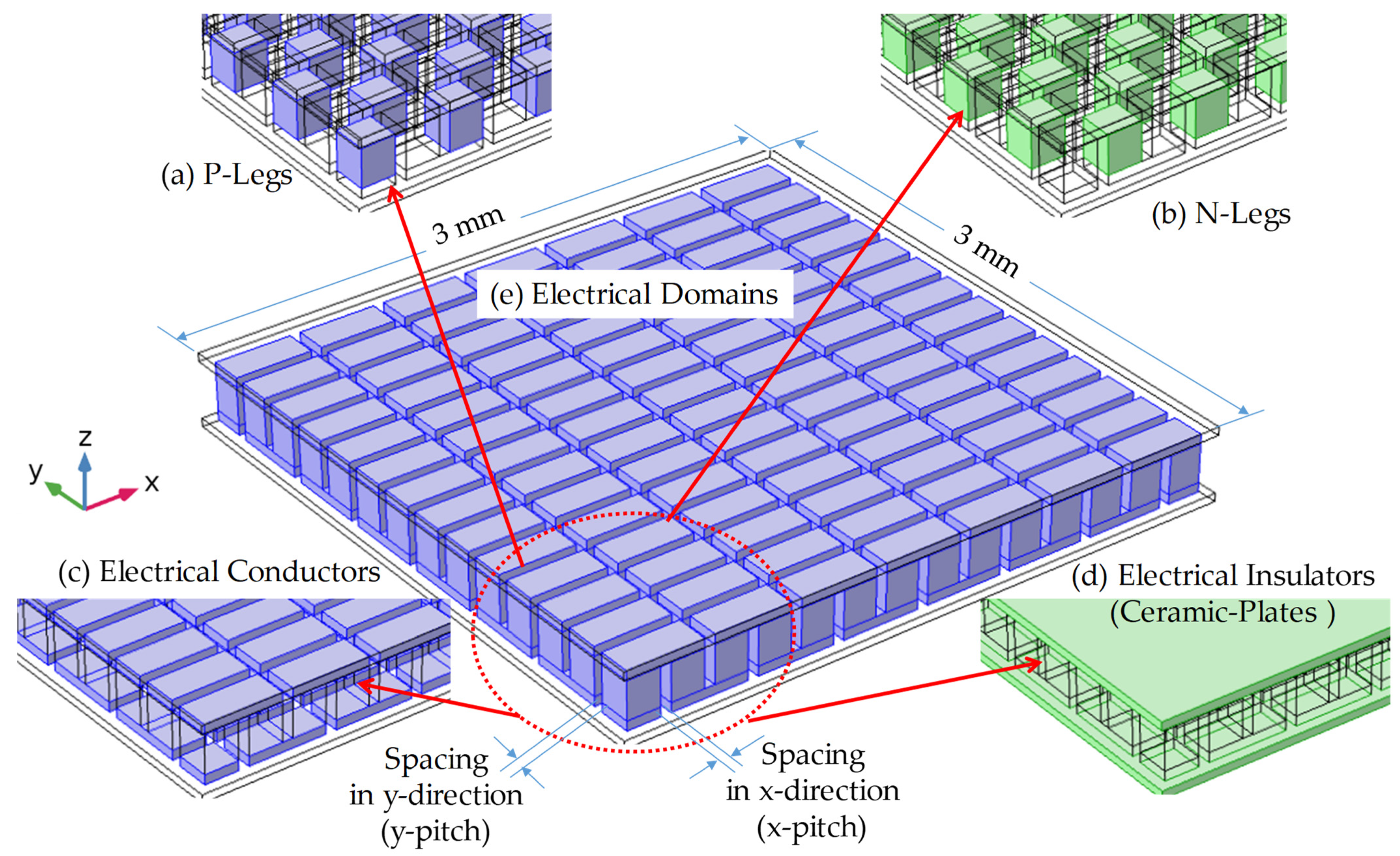
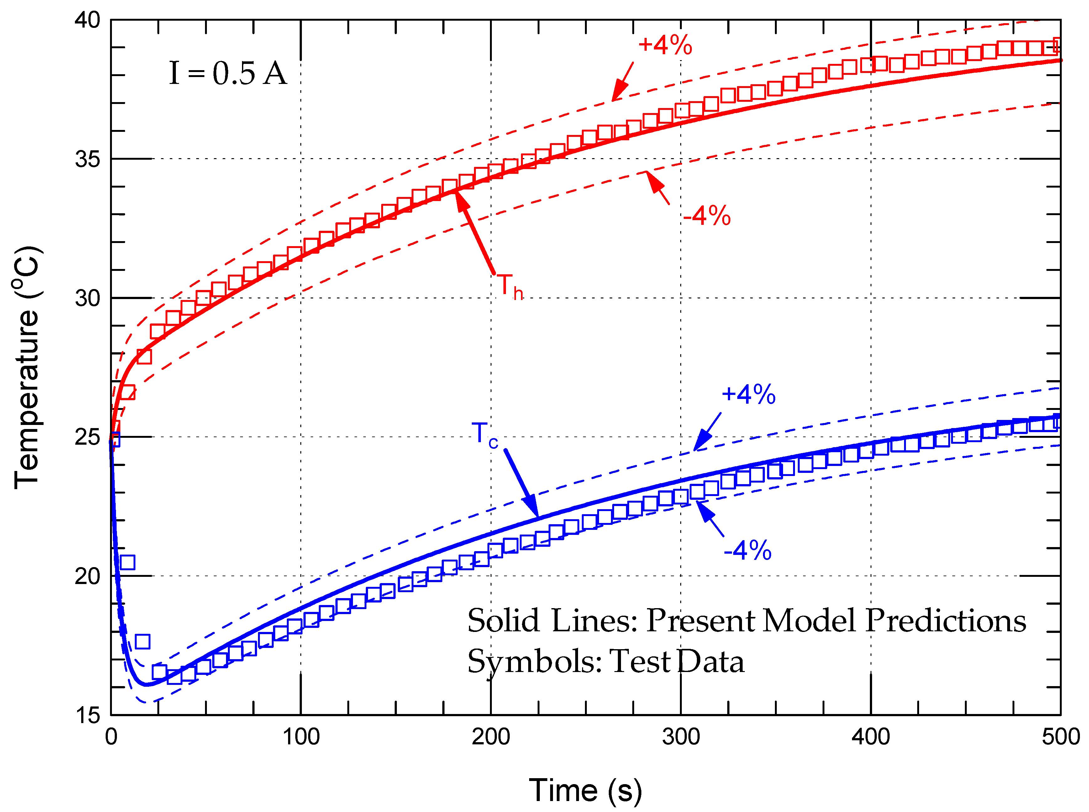
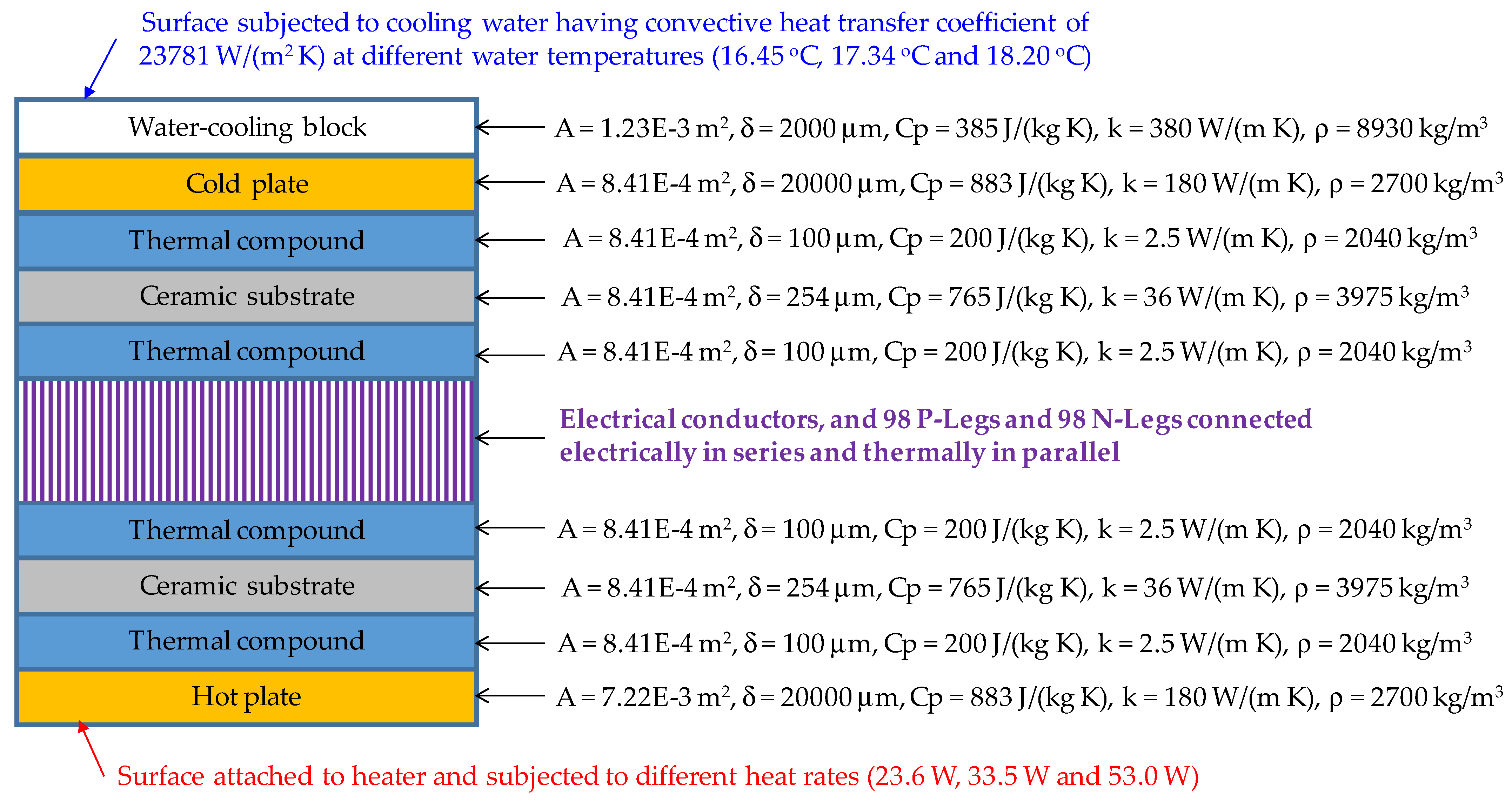
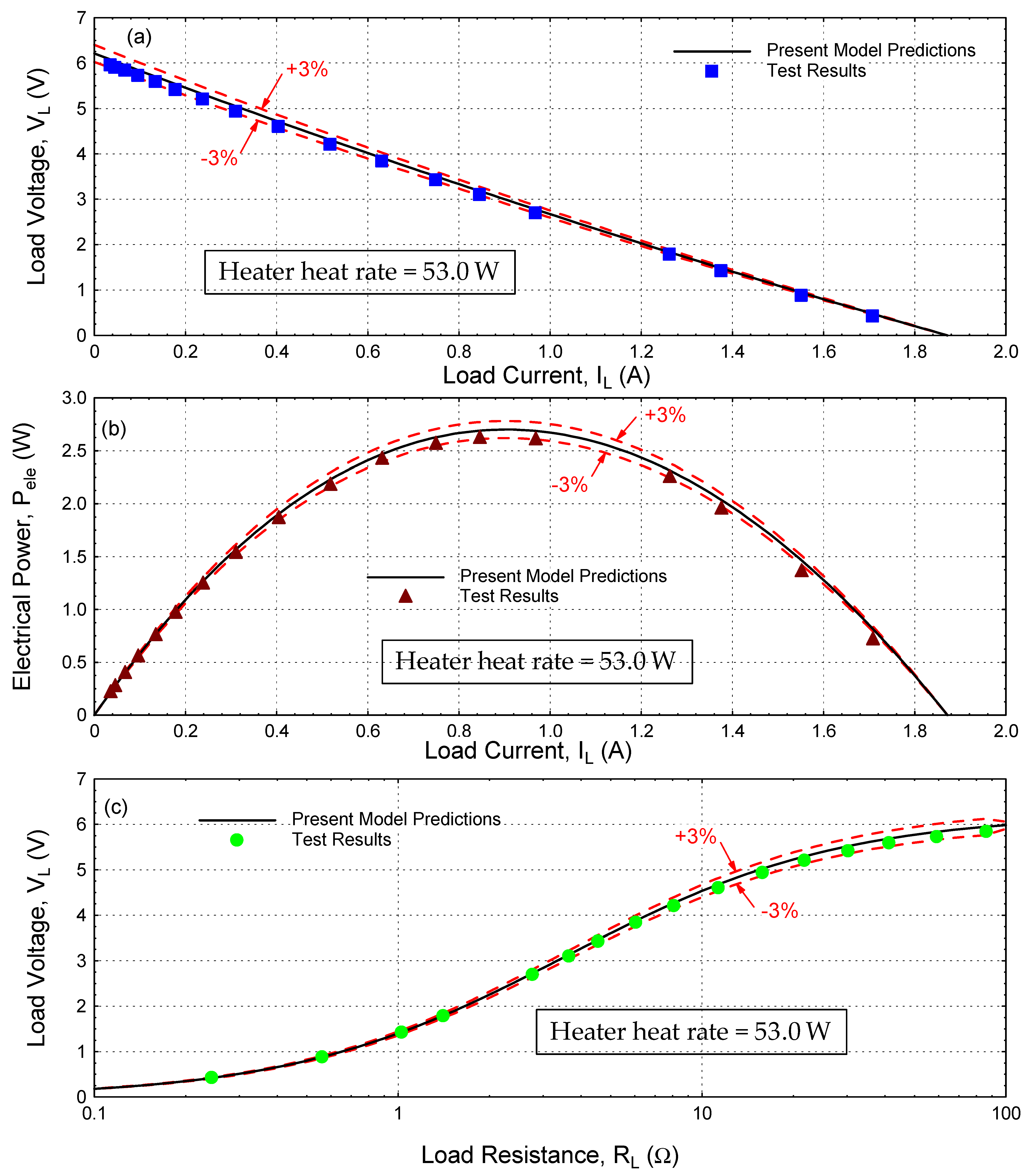
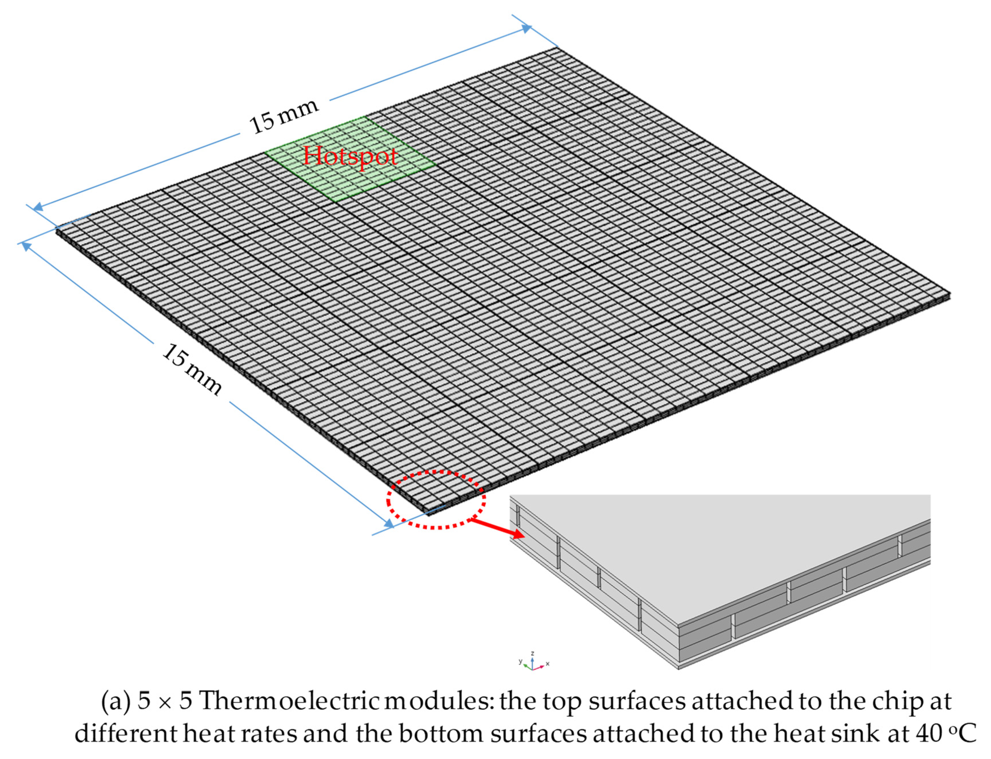
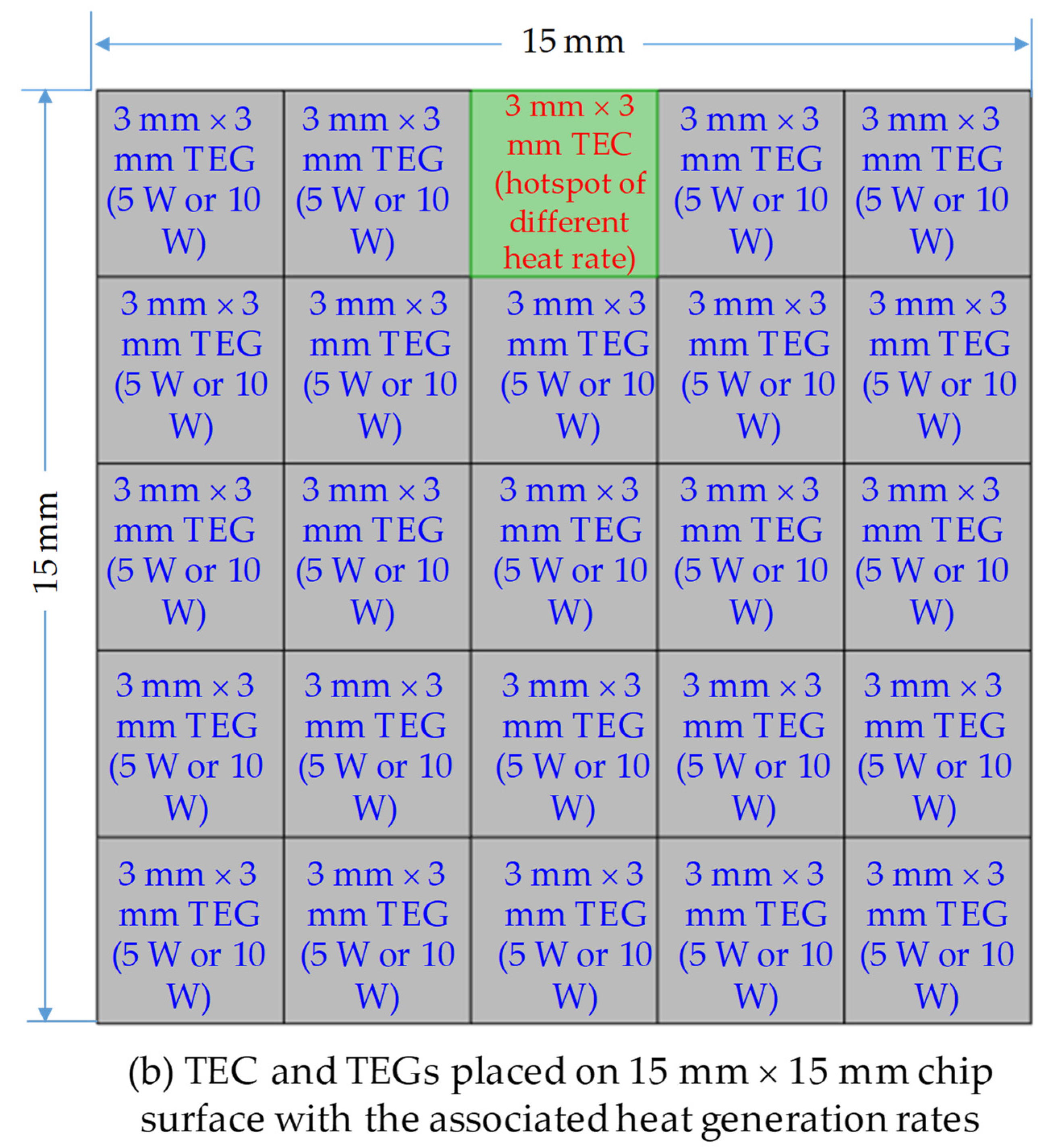
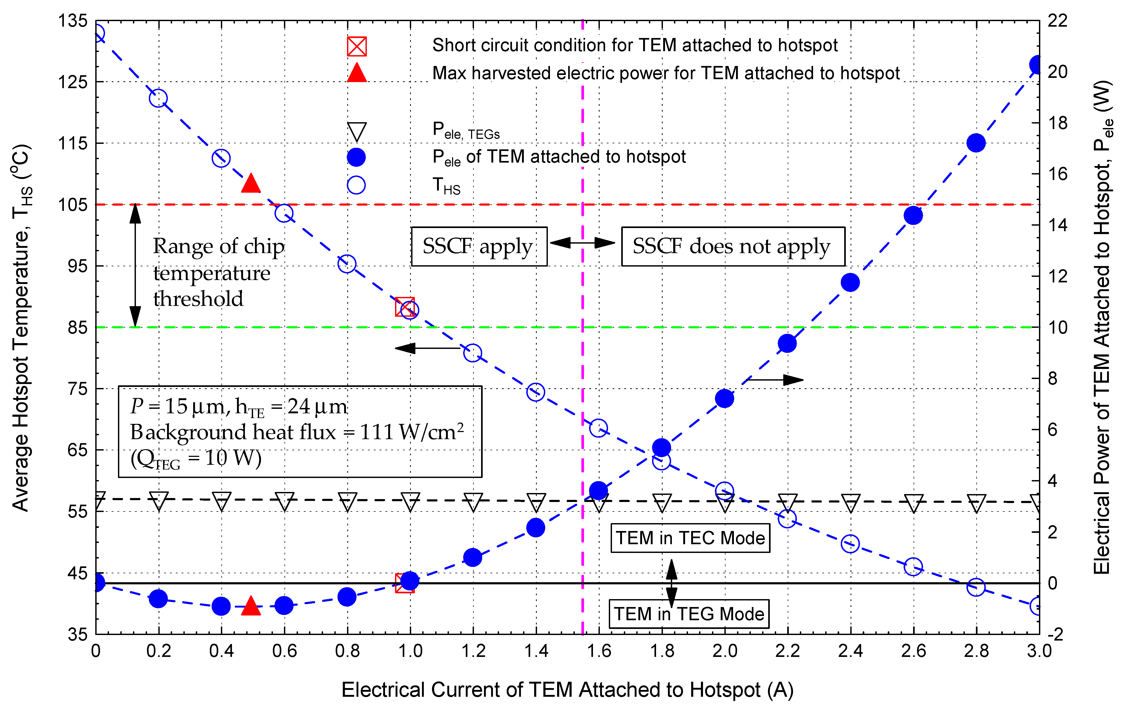
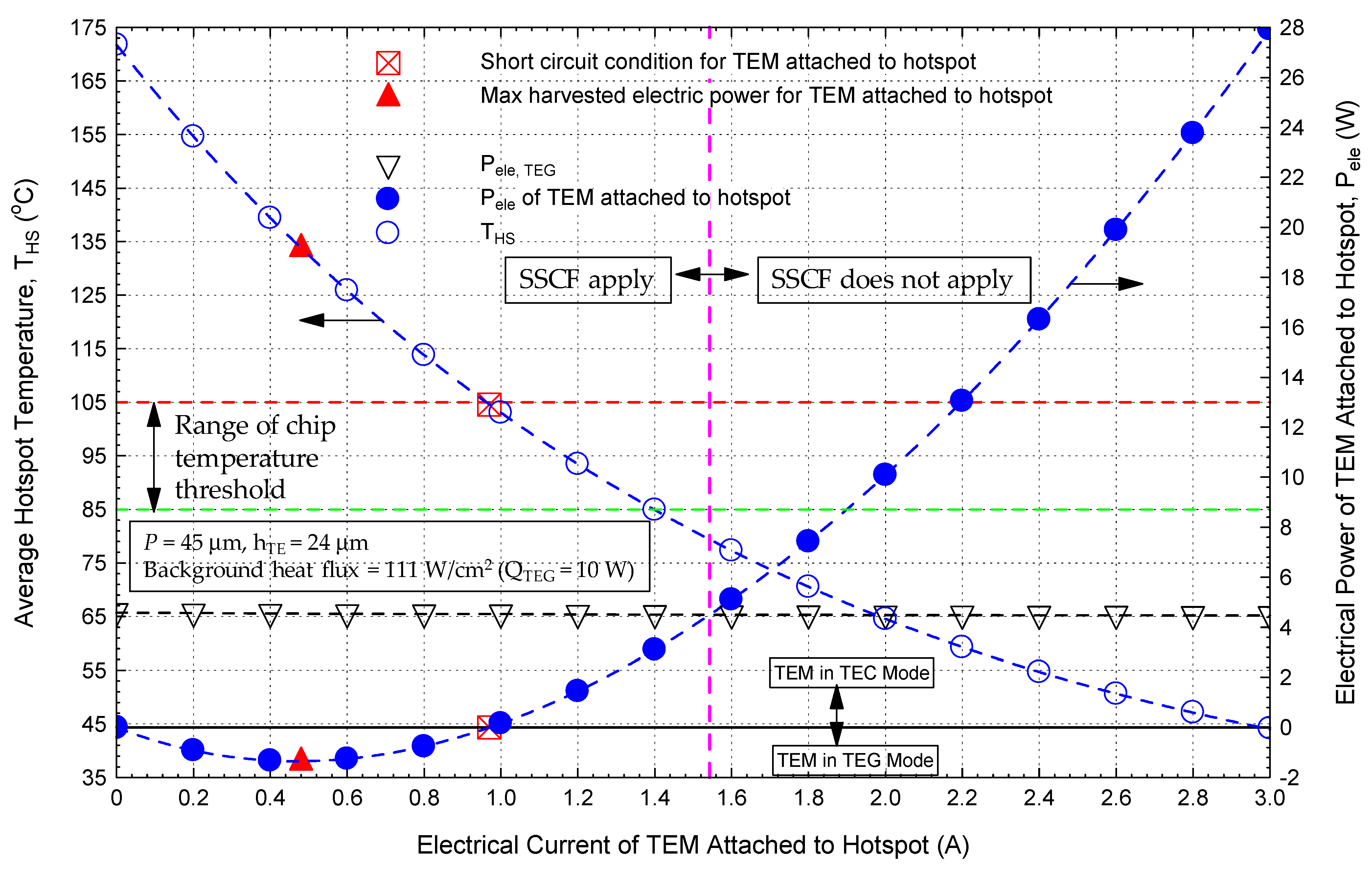
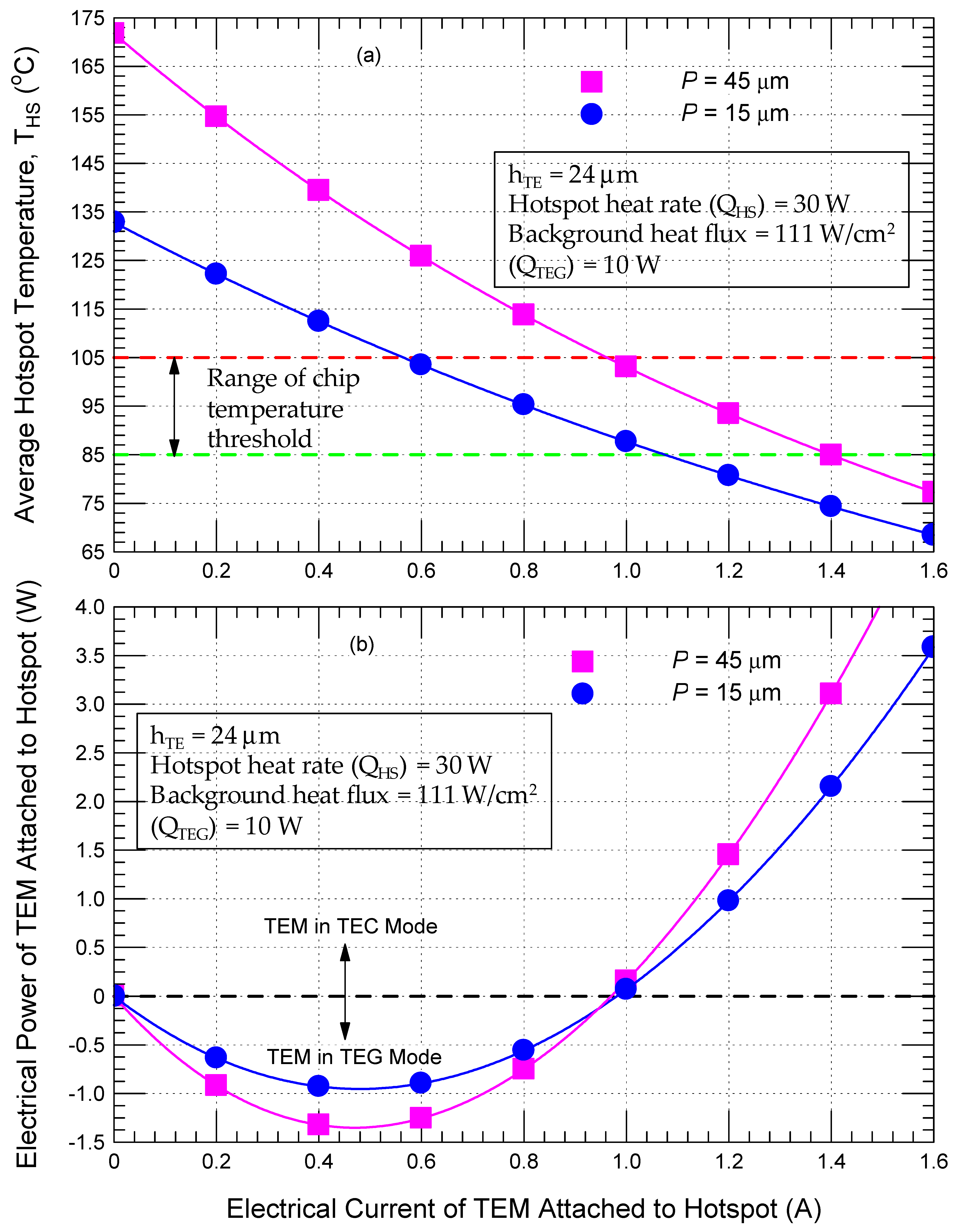
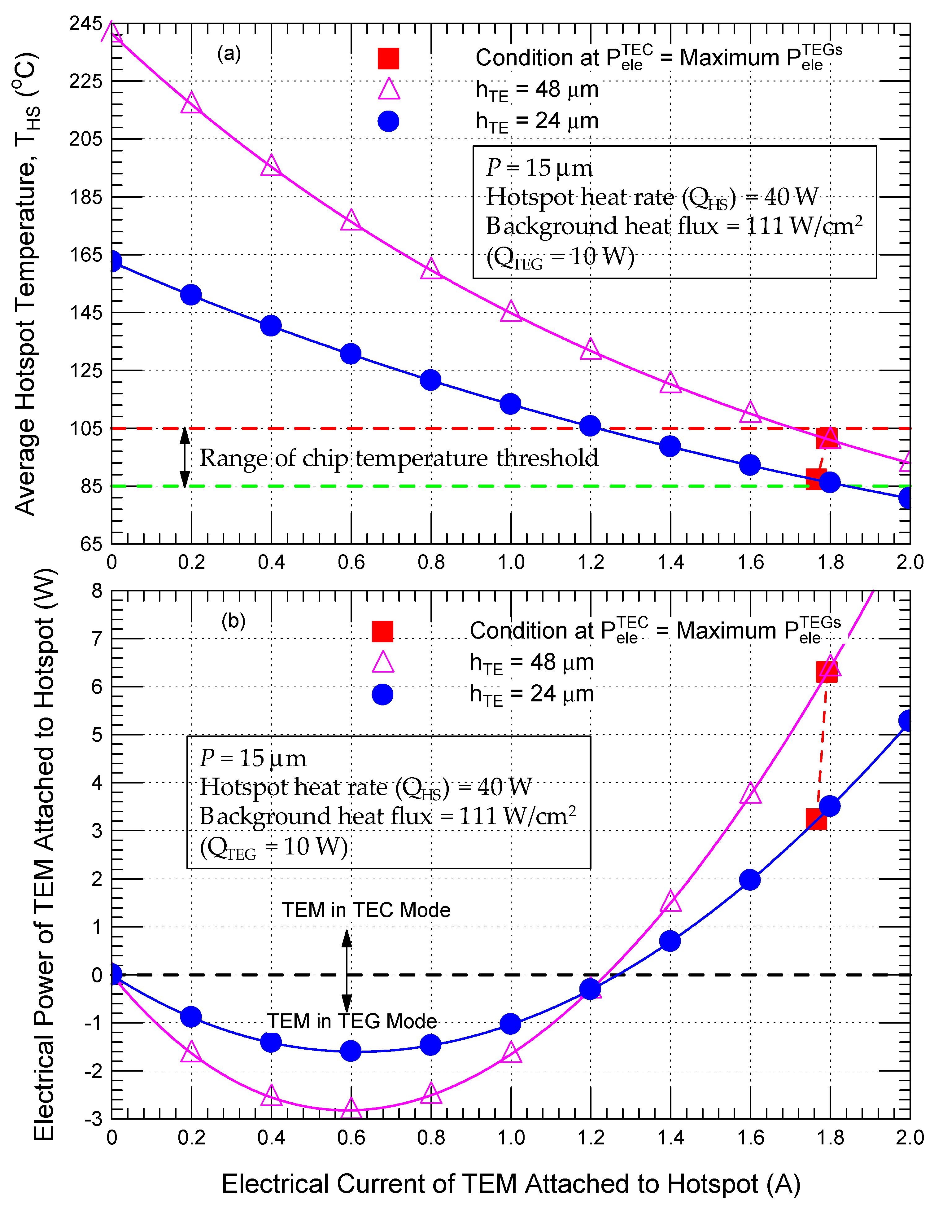
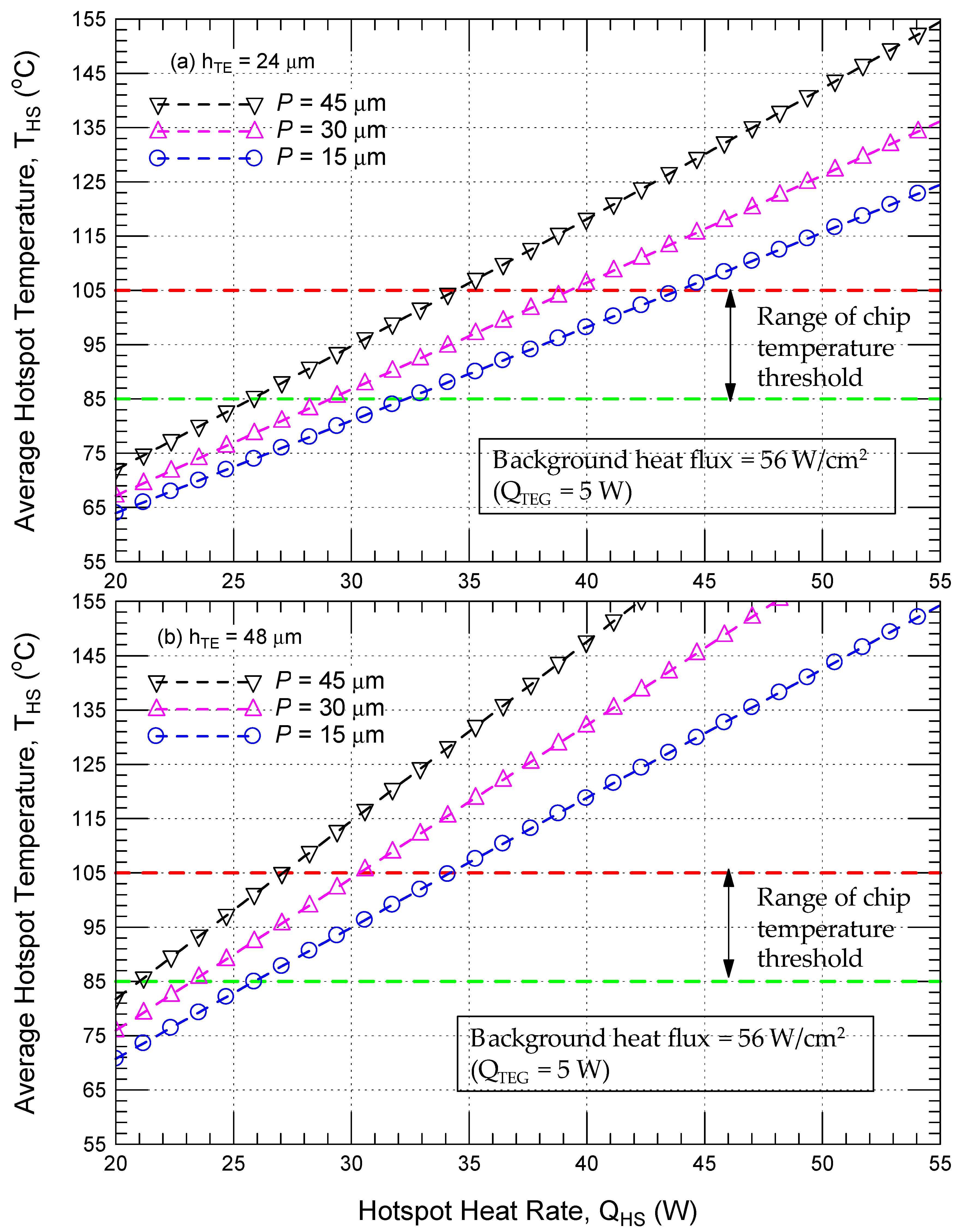
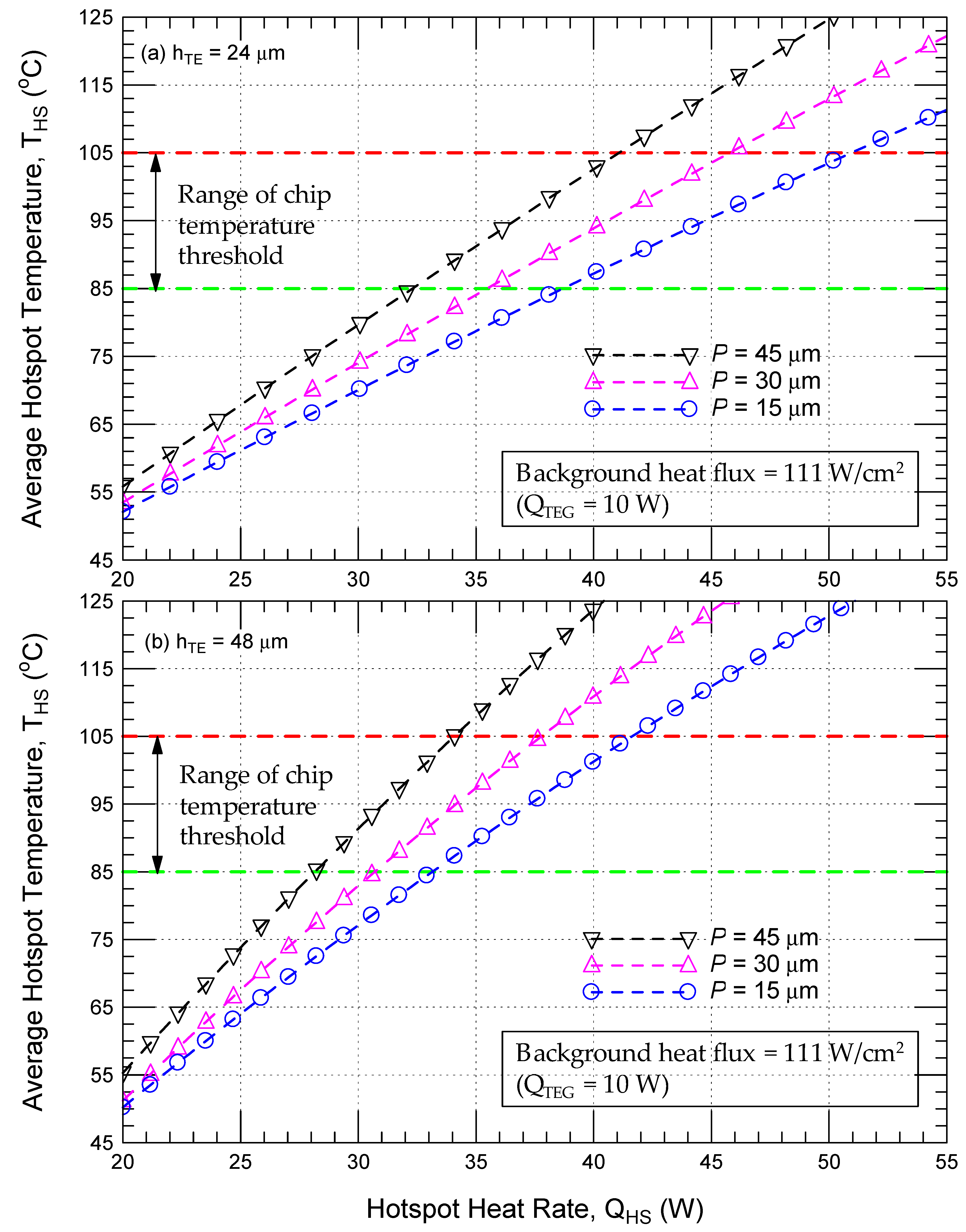
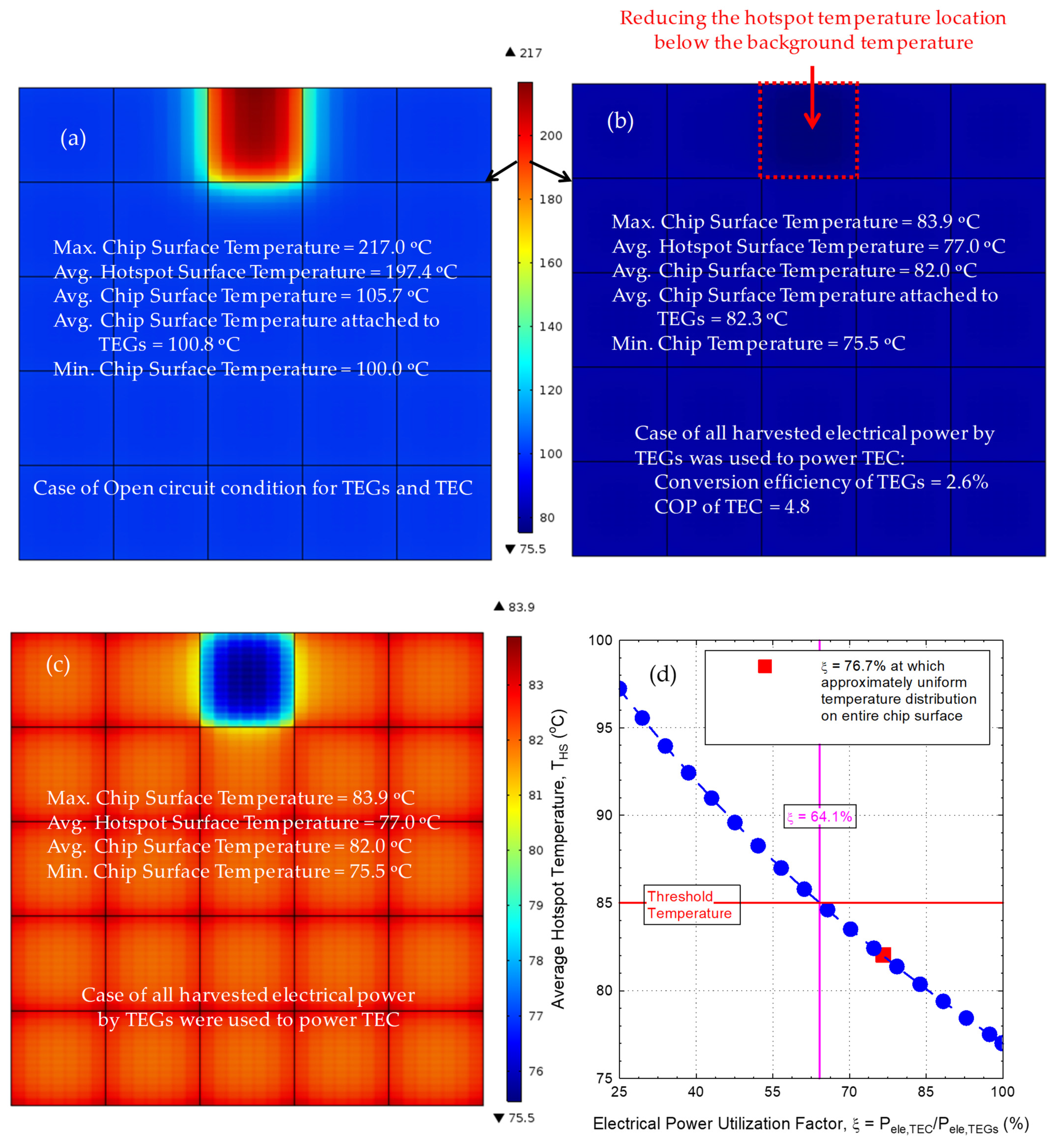
Table 1.
List of maximum hotspot heat rate of SSCF at different values of pitch (P), P-/N-leg height (hTE), and heat rate of each chip area attached to TEG (QTEG).
Table 1.
List of maximum hotspot heat rate of SSCF at different values of pitch (P), P-/N-leg height (hTE), and heat rate of each chip area attached to TEG (QTEG).
| Chip Condition | P (μm) | hTE (μm) | QTEG (W) | QHS,max (W) | qHS,max (W/cm2) |
|---|---|---|---|---|---|
| Chip manufacturer with temperature threshold value of 85 °C | 15 | 24 | 10 | 38.71 | 430 |
| 5 | 32.34 | 359 | |||
| 48 | 10 | 33.05 | 367 | ||
| 5 | 25.89 | 288 | |||
| 30 | 24 | 10 | 35.41 | 393 | |
| 5 | 29.16 | 324 | |||
| 48 | 10 | 30.62 | 340 | ||
| 5 | 23.21 | 258 | |||
| 45 | 24 | 10 | 32.24 | 358 | |
| 5 | 25.76 | 286 | |||
| 48 | 10 | 28.13 | 313 | ||
| 5 | 20.97 | 233 | |||
| Chip manufacturer with temperature threshold value of 105 °C | 15 | 24 | 10 | 50.86 | 565 |
| 5 | 43.77 | 486 | |||
| 48 | 10 | 41.66 | 463 | ||
| 5 | 34.12 | 379 | |||
| 30 | 24 | 10 | 45.8 | 509 | |
| 5 | 39.2 | 436 | |||
| 48 | 10 | 37.74 | 419 | ||
| 5 | 30.52 | 339 | |||
| 45 | 24 | 10 | 41.14 | 457 | |
| 5 | 34.38 | 382 | |||
| 48 | 10 | 34.05 | 378 | ||
| 5 | 27.12 | 301 |
Publisher’s Note: MDPI stays neutral with regard to jurisdictional claims in published maps and institutional affiliations. |
© 2021 by the authors. Licensee MDPI, Basel, Switzerland. This article is an open access article distributed under the terms and conditions of the Creative Commons Attribution (CC BY) license (https://creativecommons.org/licenses/by/4.0/).
Share and Cite
MDPI and ACS Style
Saber, H.H.; Hajiah, A.E.; Alshehri, S.A. Sustainable Self-Cooling Framework for Cooling Computer Chip Hotspots Using Thermoelectric Modules. Sustainability 2021, 13, 12522. https://doi.org/10.3390/su132212522
AMA Style
Saber HH, Hajiah AE, Alshehri SA. Sustainable Self-Cooling Framework for Cooling Computer Chip Hotspots Using Thermoelectric Modules. Sustainability. 2021; 13(22):12522. https://doi.org/10.3390/su132212522
Chicago/Turabian StyleSaber, Hamed H., Ali E. Hajiah, and Saleh A. Alshehri. 2021. "Sustainable Self-Cooling Framework for Cooling Computer Chip Hotspots Using Thermoelectric Modules" Sustainability 13, no. 22: 12522. https://doi.org/10.3390/su132212522
Note that from the first issue of 2016, this journal uses article numbers instead of page numbers. See further details here.