Flexible Sensors—From Materials to Applications
by
 , ,
, ,
Júlio C. Costa
1,* ,
,
Filippo Spina
1,
Pasindu Lugoda
1,
Leonardo Garcia-Garcia
1,2,
Daniel Roggen
2 and
Niko Münzenrieder
1,*
1
Flexible Electronics Laboratory, Sensor Technology Research Centre, University of Sussex Falmer, Brighton BN1 9QT, UK
2
Wearable Technologies, Sensor Technology Research Centre, University of Sussex Falmer, Brighton BN1 9QT, UK
*
Authors to whom correspondence should be addressed.
Technologies 2019, 7(2), 35; https://doi.org/10.3390/technologies7020035
Submission received: 28 February 2019
/
Revised: 20 March 2019
/
Accepted: 1 April 2019
/
Published: 9 April 2019
(This article belongs to the Special Issue Reviews and Advances in Internet of Things Technologies)
Abstract
:Flexible sensors have the potential to be seamlessly applied to soft and irregularly shaped surfaces such as the human skin or textile fabrics. This benefits conformability dependant applications including smart tattoos, artificial skins and soft robotics. Consequently, materials and structures for innovative flexible sensors, as well as their integration into systems, continue to be in the spotlight of research. This review outlines the current state of flexible sensor technologies and the impact of material developments on this field. Special attention is given to strain, temperature, chemical, light and electropotential sensors, as well as their respective applications.
1. Introduction
Flexible technologies can be used to fabricate devices on large substrates and to create thin and ultra-flexible perceptive systems that can be rolled or folded without altering their functionality [1,2]. Recently, this led to the development of Samsung’s and Huawei’s foldable phones [1,3,4,5]. As a whole, the market of printed and flexible sensors is expected to grow from $3.6 Billion to $7.6 Billion by 2027 [6]. This progress has been made possible by advances in materials science and device architecture which made large-scale manufacturing of flexible devices an economically viable option. Materials such as graphene, black phosphorus, or transition metal dichalcogenides have been researched for applications in gas and strain sensors. Similarly, perovskites emerged as an option to fabricate ultra-sensitive light sensors. At the same time, combinations of materials and device architectures enable the enhancement of both conductivity and deformability of flexible structures. Moreover, recent developments on semiconductors such as metal oxides, silicon nanomembranes, or organic materials has led to the fabrication of high performance circuits capable of providing on-site sensor conditioning.
Here, a review of ongoing research on flexible sensors is presented and divided in five sections. Section 2 discusses the main materials and fabrication methods currently employed for the development of sensors on flexible substrates. Section 3 shows how novel materials and structures have influenced the development of strain, pressure, temperature, humidity, magnetic, chemical, electrochemical, light and electropotential sensors. Section 4 shows the most recent techniques for modelling the behaviour of flexible sensors. Section 5 describes the advantages of flexible electronics used for on-site sensor conditioning. Finally, Section 6 investigates how these developments contribute to new applications in the fields of robotics, health monitoring and smart textiles.
2. Materials and Methods
In this section, an overview of flexible and stretchable materials employed in the fabrication of various types of sensors is presented (Figure 1). Special emphasis is placed on their most relevant properties for the development of flexible sensors, such as stability under bending, stretchability and fabrication options. The materials are divided into conductors, semiconductors, insulators and substrates, depending on the most common role each individual material has been found to perform in flexible sensors. Conductivity and transparency are highlighted for the conductive materials, whereas field effect mobility and stability under bending are the most discussed parameters for semiconductors. The dielectrics are compared based on their dielectric constant and breakdown voltage. Finally, different substrates are presented and discussed based on thermal stability, stretchability, surface quality and transparency.
2.1. Conductors
Conductive materials play important roles spanning from their application as bending sensitive layers in pressure and strain sensors to contacts on organic thin film transistors such as the ones employed on gas and bio sensors. In this section, a summary of the main conductive materials used in flexible sensors is presented.
2.1.1. Metals
Metals are some of the most commonly employed materials as conductors in both flexible and stretchable sensors. Copper (Cu) [7,8], gold (Au) [9,10,11,12,13], molybdenum (Mo) [14,15], silver (Ag) [16,17,18,19,20], platinum (Pt) [21,22], chromium (Cr) [23,24], aluminium (Al) [25,26,27,28], nickel (Ni) [11,29] and magnesium (Mg) [30,31] have all been widely used due to their intrinsic electrical conductivity and high mechanical stability under bending stress down to micrometer scale [32]. Au has been extensively used in the form of thin-film metallic contacts due to its resistance to oxidation. When using this material, underlayers of titanium (Ti) or Cr are typically used to increase the adhesion to the substrate [33,34,35,36]. Also, Mg has recently been employed as a contact due to its biocompatibility (Figure 2a). In addition, metal thin films can be easily deposited on flexible substrates through conventional techniques such as electroplating [37,38,39], sputtering [15,23], thermal/e-beam evaporation [9,22,40], and solution methods [19,41,42]. Nevertheless, although these materials are adequate for flexible applications, they are not easily employable in stretchable scenarios in the form of thin films, unless delicate substrate modifications are applied [32,43,44]. In addition, they are not transparent even in the form of nanometer thick films. This is an important property in applications that benefit or depend on transparency in the visible spectrum such as photodetectors.
The application of metals in different geometries, such as metal nanowires, nanoparticles and metallic liquid conductors, has been carried out to fulfill requirements like flexibility, stretchability and transparency. These open the possibility for highly stretchable conductive films and are more adequate for printed electronics. In this context, copper nanowires (CuNWs) [45], gold nanowires (AuNWs) [46,47], silver nanowires (AgNWs) [17,48] and liquid metals [49,50,51,52] show the most promising properties for highly stretchable electrodes. Metal nanowires can be fabricated by either solution processes (bottom-up approach) or by template/patterning methods (top-down approach) [53]. The top-down approach relies on the patterning or template assisted growth of mesh-like metal structures and allows the fabrication of perfectly aligned NWs [54]. The drawbacks from these techniques arise from their complexity and, in the case of template assisted methods, from the presence of undesired materials on the NW structure. Conversely, solution processes can fabricate large numbers of NWs with controlled dimensions. In addition, solution processes are more compatible with large area fabrication [55,56].
CuNWs have been widely explored as stretchable conductors, nevertheless, the tendency of Cu to easily oxidise in contact with air hinders its direct application in flexible sensors [45]. AuNWs also present high conductivity and transparency values. Gong et al. [46] demonstrated a Au nanomesh formed by the self-assembly of solution processed AuNWs which presented a sheet resistance of /square (/☐) and a transparency around 92%. Although with a lower transparency (60%), Lee et al. [47] achieved a sheet resistance of 3 /□ for a Au metal grid with a line width of 3 . However, due to the high price of Au and the easy oxidation of Cu, Ag is more widely used. One of the main issues with the conductivity of NWs resides on the elevated junction resistance. To solve this issue, welding of AgNWs using light sources has been investigated, as illustrated in Figure 2b [48]. Based on a similar approach, using a purpose-built, ultra-fast and laser-induced plasmonic welding system (LPW) improved the junctions of roll-to-roll printed AgNWs on PET [17]. The sheet resistance decreased from 450 /□ for unwelded AgNWs films to 5 /□ when these were exposed for a period of . At the same time, the transparency did not drop below 90% in the visible range. The films processed by LPW also showed outstanding bending stability with minimal to none change in resistance when curved from 0 to / [17]. Recently, Oh et al. [57] used Ag flakes sintered on a stretchable silicone elastomer substrate (Ecoflex™) using a custom-made intense pulsed light system (Figure 2c). This sintering process works based on the photothermal effect, where the Ag flakes are welded together in a short amount of time, thus avoiding any damage to the substrate. Using this approach the devices could withstand a 500% strain while maintaining a resistance below 200 . In an alternative approach, the combination of AgNWs with other conductive materials, such as carbon nanotubes (CNTs), has also resulted in highly conductive (27 /□), conformable (500% strain) and transparent layers (>90%) without the need for complex sintering processes [58].
Liquid metals present the highest conformability factor of all the conductive materials. Among them, the most widely used are eutectic gallium-indium (EGaIn) and mercury (Hg) [59,60]. Due to its toxicity, Hg is not preferable for flexible sensors. On the other hand, EGaIn is biocompatible and has been extensively employed in the fabrication of flexible electronic components [49]. This material presents a conductivity of / [50]. In addition, EGaIn’s unique rheological and self-healing properties are provided by an elastic thin skin made of gallium oxides, which prevents the liquid from withdrawing from microchannels. Moreover, the material’s low viscosity ( · ) promotes the filling of microcavities in the channels [51,52]. These properties make liquid metals suitable for fabricating highly stretchable and self-healing conductive contacts and electrodes [61].
2.1.2. Amorphous Oxide Conductors
Indium-tin-oxide (ITO), aluminium-zinc-oxide (AZO) and indium-zinc-oxide (IZO) are a class of materials commonly known as transparent conductive oxides (TCOs). These materials were initially used as infrared (IR) reflective layers on windows, as their plasma frequency sits on the IR part of the electromagnetic spectrum. Later, with the introduction of ternary compounds showing higher electrical conductivity, these materials started to be widely applied as transparent conductors in the development of flat panel displays [62,63]. This transition in applications was made possible by the development of ITO. ITO is an n-doped tin (Sn) form of In2O3. This doping process results in excellent metal-oxide orbital overlaps and, subsequently, on a low electron effective mass. This overlap results in larger electron mobility, which, together with the wide band-gap and low plasma frequency of this material, result in high conductivity and transparency [63,64]. ITO combines high transparency in the visible range (>80%) with a low electric resistivity ( ) [64]. In addition, ITO can be deposited by DC [65,66,67,68], and RF sputtering at low temperatures [69], making it compatible with polymeric substrates. For these reasons, ITO has been widely used as a transparent electrode in flexible sensors [20,70,71,72,73,74,75,76,77]. Nevertheless, resistivity values below are not easily obtained for fabrication processes at room temperature [67]. Additionally, ITO is not highly bendable, and 20 thick ITO layers present critical bending radii around [78]. Furthermore, films of ITO on polyethylene naphthalate (PEN) or polyethylene terephthalate (PET) can suffer significant damage when bending around a 10 radius [78]. To replace ITO, IZO has also been recently used for the development of flexible sensors as a contact material [79,80]. Due to the cost and scarcity of In, there is interest in substituting In in TCOs. For this end, materials with interesting properties for flexible electronics, such as AZO, have been developed. Zhou et al. [81] demonstrated that an AZO/Au/AZO layer on mica exhibiting a sheet resistance of 5 /□ and a transparency close to 90% for a total layer thickness of 126 where the Au layer corresponded to 10 . This device withstood a 7 bending radius, but its sheet resistance increased to 9 /□ while bent to a smaller radius of 5 .
2.1.3. Carbon Conductors
In 2004 the introduction of exfoliated few-layer graphene (FLG) by Novoselov et al. [82] led to a dramatic increase in the interest on carbon-based materials. The combination of its high carrier mobility (as high as 20,000 cmVS for electrons on a graphene field effect transistor (FET) [83]), with the ability to sustainably conduct high currents ( A/), made this material very attractive for the development of thin film transistors [84,85], battery electrodes [86], and sensors [87]. In the field of flexible electronics, carbon-based materials have found most of their applications as electrical conductors and can be found in various formats including CNTs [88,89], CNT fibres [90,91,92], graphene [93,94,95,96], reduced graphene oxide (rGO) [97,98,99], carbon black (CB) [100,101] and graphite [102,103,104,105]. Graphene is a 2D material that presents both the properties of a conductor and a semiconductor [106]. High quality graphene can be obtained by methods such as chemical vapour deposition (CVD) and both mechanical and chemical exfoliation [93]. Mechanical exfoliation, i.e., the scotch-tape method [82], is capable of producing high quality graphene but the dimensions and the manipulation of the individual layers are difficult to control. Chemical exfoliation is a widely used method for the development of flexible sensors. This method relies on the oxidation of graphite into graphene oxide (GO), followed by the reduction of this compound to form rGO. This step is usually incomplete leaving leftover functional groups across the graphene layers which reduce their conductivity, but also increase the sensitivity of rGO to various chemicals. This allows the fabrication of chemical sensors [107,108,109,110]. CVD graphene is also very interesting for the development of flexible sensors due to its large area fabrication potential. Figure 3 shows the growth relation between the temperature and the quantity of carbon precursor present at the surface of the metal catalyst [111]. As can be seen, by controlling these parameters, both thin and thick films of FLG and single-layer graphene (SLG) can be obtained. Typical metals used as a catalyst for CVD graphene are Ni and Cu. In addition, the grown graphene can be transferred to any substrate by the deposition of poly(methyl methacrylate) (PMMA), followed by the etching of the metal layer. The floating graphene/PMMA surface is then deposited on the desired substrate.
CNT fibres have also attracted considerable attention in the field of flexible sensors and devices. CNT fibres consist of large numbers of aligned CNTs. CNTs are 1D conductors composed of either a single “rolled” graphene layer, resulting in single-wall CNTs (SWCNTs), or of multiple nanotubes which share the same core to form multi-wall CNTs (MWCNTs) [106]. To date, electrical resistivities as low as for iodine doped CNT fibres have been obtained [112]. Furthermore, tensile strengths in excess of 9 have also been reported [113]. These properties, combined with their strain resistance (up to 285% strain at failure for coiled fibres [114]), make these structures ideal for flexible and stretchable applications [90,115,116]. CNT fibres can be easily fabricated from a CNT solution and deposited by wet-spinning or through dry-spinning from a nanotube forest floating catalytic chemical-vapor-deposition (FCCVD) reaction zone [117].
2.1.4. Organic Conductors
Organic conductors are polymers with intrinsically conductive properties, also known as electrically conductive polymers (ECP), intrinsic conductive polymers (ICP), or simply as conductive polymers (CP), and are functional materials with the electrical, magnetic, and optical properties of metals, but with the conventional mechanical properties of a polymer [118,119]. The electrical conductivity of CPs can be tuned, ranging from / to / [120]. CPs are formed either through chemical oxidation or electrochemical oxidation of monomers, being the most widely used polypyrrole, polyaniline (PANI), and derivatives of polythiophene, such as PEDOT [121,122]. CPs are preferred to metals in the fabrication of flexible electronics as they possess a higher malleability, flexibility, and biocompatibility [123].
The primary oxidation of aniline is polyaniline (PANI), also called black aniline [124]. PANI is an ICP with good stability over time and has a tunable electrical conductivity. The variation of the conductivity relies on the degree of doping, oxidation state, particle morphology, crystallinity, interior intra-chain interactions, or molecular weight [118,123,124,125,126]. PANI can become more conductive after proton doping or can decrease its charge carrier if gas molecules are absorbed. Its ability to change the conductivity is of interest for the fabrication of chemical and biological sensors [127,128,129,130,131]. PANI’s base conductivity for an undoped sample was reported to be /, and the highest conductivity observed was / for a sample doped with HNO4 [132]. PANI’s conductivity can also be increased with the use of carbon materials such as graphene [125,129], rGO [130], graphite [126,128,129], graphene nano platelets (GNP) [129], or MWCNTs [133]. Despite its good electrical properties, PANI is used in composites due to its lack of stiffness (modulus = ) [134]. This material also possesses a high infusibility, poor solubility and melting processability, and good adhesion, making PANI a material highly used as a coating on flexible surfaces [126]. The main methods for the preparation of composites are impregnation by wetting [118,123,127], spraying [133], electrodeposition [126,128,129,131], electronic polymerisation [125], and oxidative polymerisation [135]. Park et al. [136] reported the fabrication of PANI nanofibres by potentiodynamic growth (Figure 4a) with a sheet resistance of 420 /□. Materials such as sponges [127,130], cotton and polypropylene woven fabrics [133], cotton and polyester knit fabrics [128], or nano cellulose fibrils with high tensile modulus have been impregnated with PANI to sense humidity and gases [118]. This material can be either doped with hydrochloric acid (HCl) and phosphoric acid (H3PO4) to improve the protonation [128], or functionalised with MWCNTs to obtain a resistance of 2280 and a bendability up to 240 [133]. Impregnation of cellulose nanofibrils with PANI reported an improvement on their properties (conductivity / and high thermal stability at 500 with a modulus of ) [118]. The implementation of PSS to replace highly acid solutions that reduce PANI’s conductivity, such as hydrogen chloride (HCl), was carried out to increase the conductivity to /, with a further enhancement in the conductivity ( /) by using PSS-coated graphene sheets with a PSS-doped PANI solution (Figure 4b) [125].
Thiophene-based organic conductors such as polythiophenes (Tn), tetraethylene-glycol polythiophene (TEGPT) [137], or p-poly(3,4-ethylenedioxythiophene) (PEDOT) [138,139,140,141], have also been adopted for the fabrication of flexible sensors for bio-recognition. TEGPT functionalised with biotin (b-TEGPT) films were reported to be inkjet-printed on paper substrate by Ihalainen et al. [137], obtaining a conductivity in the range of 10 × 10−7 / to 10 × 10−6 /. However, PEDOT is one of the most prominent polythiophenes with high conductivity and good filming properties that made it broadly used in electric and electronic applications (antistatic coating, electrically conductive coatings, thermoelectric materials, field effect transistors, and active material for electrochemical devices), and is also widely used for flexible sensor applications [138,139,140,141]. PEDOT is usually polymerised in the presence of polystyrene sulfonate (PSS), forming an aqueous dispersion of high relevance for the fine film formation of PEDOT:PSS [140]. PSS acts as a container for the charge balancing counter ions, being closely associated through the electrostatic attractions with PEDOT, and contributes to the stability of the colloid by keeping the PEDOT segments dispersed in the aqueous solution [122,138]. PEDOT:PSS also possesses a better aqueous stability and biocompatibility than PPy and PANI, and it is considered a promising polymer for continuous sensing and even for in vivo implantations [142]. PEDOT:PSS films have a stable conductivity ( /) that can be tuned by chemical modification dependent on the nature and degree of doping, achieving a conductivity of 30 / with a baseline resistance 38 / [139,143]. Flexible sensors can be fabricated using PEDOT:PSS by electrodeposition [143,144], aqueous dispersion [139], mixing [139], inkjet printing (Figure 4c) [145], spraying [146], chemical oxidation [147], vapor deposition polymerisation (VDP) [147,148], and can be patterned via photo lithography [149]. PEDOT:PSS exhibits excellent electric transport properties for large surface areas and promotes a higher electrocatalytic activity making this material ideal for the fabrication of solar cells [144,150,151]. The addition of carbon materials, such as MWCNT, graphene powder or graphene oxide, increases the efficiency, enhances the electrocatalytic performance, sensing stability and reduces the charge transfer resistance [139,141,144,150,151,152,153,154]. The heterojunction of silver nanoparticles (AgNP) and PEDOT:PSS has been observed to increase the thermoelectric coefficient [145]. This material has been used on SWCNT-stretchable and transparent electrochemical sensors, where PEDOT:PSS was used as conductive coating and binder (Figure 4d), enhancing the electrochemical performance and reducing the sheet resistance of the SWCNTs (145 /□ to 73 /□) [154]. PEDOT:PSS can also be used with bilayer enzyme electrodes, obtaining highly reliable and resolved amperometric signals in response to glucose concentrations [142], or to create biodegradable electrodes with a conductivity of 12 (19% concentration of PEDOT:PSS), and a charge storage of 74 / [149]. Wang et al. [139] prepared a composite of MWCNTs on carboxylic group functionalised graphene (GR-COOH) into aqueous dispersion of PEDOT:PSS with a conductivity of / and enhanced to / when immerse in double distilled water for 24 . Similarly, Kumar et al. [140] demonstrated that the conductivity of a paper made of nanocomposites formed by PEDOT:PSS and carbon nanotubes (CNTs) can be increased from / to / (caused by the removal of PSS molecules), when treated with formic acid. When graphene powder is dispersed in PEDOT:PSS the conductivity was increased up to /, and the response improved from 9.6% to 15.8% under a bending test at 70 [141]. Similarly, graphene/PEDOT:PSS composites showed a better sensitivity in terms of relative resistance variation (0.0236) than graphene Ag colloids (0.0321) [153]. Further enhancements on the carrier transport can be achieved by an increase on the surface area with the fabrication of nanostructures, such as nanotubes (conductivity of 61 /) or nanocables (conductivity of 71 /) [147]. Mixtures of graphene and PEDOT:PSS have also been sprayed on PET yarns, achieving a surface resistance of 300 Ohms and a capacitance of 541 reaching up to 375 / [146]. Non-conventional geometries were employed to build a wrinkled energy harvester and sensor [122], which was achieved by depositing PEDOT:PSS on a stretched polydimethysiloxane (PDMS) substrate (distance of ≈ 5 , thickness of ≈ ). The PEDOT:PSS layer presented a sheet resistance of 1.4 /□ to 4.63 /□ which increased to /□ when stretched at 100% [122]. Besides, surface modification of PEDOT:PSS nanotubes with nanorods or nanonodules, as observed in Figure 4e, have been implemented to increase the surface area, thus improving sensitivity, bendability and durability [148]. Furthermore, PEDOT:PSS has also been reported to be used in heat flux sensors on PEN flexible substrates to improve the thermopower up to 161 / with no degradation after encapsulation, and testings for bending and torsion [155].
Polypyrrole (PPy) is also an environmentally stable and biocompatible ECP, with a high electrical conductivity in the range 40 / to 50 / [156,157], and with a mechanical flexibility and solubility that makes it easy to apply on fibre surfaces through bathing [158,159,160,161], electrodeposition [161], or in-situ polymerisation [70,157,162,163,164]. PPy has been used as conductive coating on carbon fibres and PDMS-carbon fibre bundles via electropolymerisation to create a fibre-based e-skin capable of self charge through triboelectrification effect [164]. PPy has also been used for the fabrication of porous structures using PDMS, BaTiO3 nanoparticles and PMMA to prevent structural failure when fabricating a stretchable device (310%) with a conductivity of / [161]. Devices have been manufactured using PPy on cellulose sponge through oxidative chemical deposition and anthraquinone-2-sulfonic acid (AQS), which induced the formation of PPy nanoparticles and nanowires on the sponge fibres surfaces, obtaining a maximum sheet resistance of 120 /□. PPy was used to coat a polyurethane (PU) porous structure to fabricate a highly stretchable device (420%), with a maximum resistance of /, where also net-like microcracks were formed, making possible the reversible electric resistance under stretching [158]. Structure of polymers such as PVA nanowires (PVANW) and PDMS fibres elastic membranes have been used as structural elements for PPy. PVANW was electrospun on PET/ITO to form a stable structure, where synthesised PPy film was deposited on PVANW-PET/ITO to fabricate a piezoresitive wrinkled sensor. Similarly, PPy was deposited on an elastic membrane made of PDMS fibres, obtaining a flexible strain sensor with a specific volume resistance of 448 [162]. A more complex structure was achieved by Park et al. [157] where a pressure/temperature/strain sensor and a flexible capacitor was fabricated in a single device. They used a PDMS coated microporous polypyrrole/graphene foam composite (PDMS/PPy/GF). The substrate used was made of a mixture of PDMS and Ecoflex™, patterned with GaInSn. The porous structure was formed using graphene CVD on Ni foam, where the PPy was electrochemically deposited and the Ni removed. This structure was coated with PDMS to provide structural support. PPy/GF provides a high conductivity /, a large surface area, and a Seebeck coefficient of /. Furthermore, PPy synthesised with methyl orange (MO) was found to increase its conductivity, being the maximum of /, although MO at higher concentrations can reduce the conductivity [163,165].
In summary, metal thin films continue to represent the easiest and most common approach for the fabrication of contacts on flexible sensors. However, metal nanowires and CNT nanofibres are better suited for stretchable applications and facilitate transparency. More specifically, sintered AgNWs present optimal properties and have the potential to replace ITO as transparent conductors on flexible applications.
2.2. Semiconductors
Typical crystalline semiconductors such as silicon (Si) and germanium (Ge) rely on covalent bonds for the transport of charge carriers. Due to the high structural order of these semiconductors, their mobility is high ( 2−1−1) and is mostly limited by phonons (lattice vibrations), impurities and other carriers [166,167]. Nevertheless, these materials are rigid and, as such, cannot be applied for truly flexible and conformable electronics. Semiconductors play crucial roles in sensors and are mainly used as either the channel of the thin film transistors (TFTs) used for the development of on-site signal conditioning circuits or as sensitive layers. This section presents the current status of the semiconductor materials currently employed in flexible sensors.
2.2.1. Metal Oxide Semiconductors
Among metal oxide semiconductors, the most widely used material in flexible sensors as a TFT channel is amorphous indium-gallium-zinc-oxide (a-IGZO) [14,15,23,24,32,33], while ZnO is widely used for electromagnetic radiation sensors [21,73,74,168,169,170,171,172]. Other metal oxides which have also been used in flexible sensors as semiconductors are indium-zinc-oxide (IZO) [173,174], and tin-oxide (SnO) [175,176,177]. In metal oxide semiconductors, the carrier transport relies on the overlap of spatially spread ns orbitals belonging to the metal cations [178]. For this reason, metal oxide semiconductors have mostly been confined to n-type [179].
The wide adoption of n-type a-IGZO for flexible circuits and sensors arises from its mechanical stability when bent down to micrometre range radius [180], and low temperature processing options such as DC sputtering [14,181], RF sputtering [15,23,33,36], and solution methods [182,183], resulting in large area and polymer processing compatibility. In addition, electron mobilities in excess of 70 2−1−1 [184], and Ion/Ioff above 1010 have been reported [185]. Yao et al. [186] recently presented a method to deposit a-IGZO on polyimide (PI) substrates through pulse DC magnetron sputtering. Excluding a 1 150 photoresist bake, the whole process was conducted at 22 . Flexible a-IGZO TFTs fabricated using this technique showed saturation mobility up to 2−1−1, Ion/Ioff above 107 and subthreshold swing of 320 / [186]. In addition to a-IGZO, flexible ZnO has also been widely used in flexible sensors, where it finds most of its applications as the sensitive layer of UV sensors due to its bandgap ( ) [187], large exciton binding energy (60 ) [187], and high mobility above 50 2−1−1 [188]. Boruah et al. [187] showed that the light-harvesting efficiency (LHE) of ZnO improved for self-assembled microstructures when compared to conventional thin films. More specifically, the LHE for ZnO films increased from 30% to 84% for ZnO nanorods, and furthermore to 98% for vanadium (V) doped ZnO nanoflakes. Due to the advantages offered by the properties exhibited by metal oxide semiconductors, they have been widely employed in flexible sensors.
2.2.2. Organic Semiconductors
Organic semiconductors (OSC) can be small molecules or polymers, such as pentacene, poly(3-hexylthiophene) (P3HT), poly(diketopyrrolopyrrole-terthiophene) (PDPP3T), 5,5-bis-(7-dodecyl-9H-fluoren-2-yl)-2,2-bithiophene (DDFTTF) or polyisoindigobithiophene-siloxane (PiI2T-Si). They are flexible and their fabrication is simple, low-cost and can be performed at low temperature when compared to non-organic semiconductors. OSCs can modulate their conductivity, are highly responsive to chemical agents and are widely used in flexible chemical sensors based on organic field-effect transistors (OTFTs) [189,190,191,192]. PiI2T-Si has a mobility of 2−1−1, and has been used to fabricate flexible sensors on PDMS substrates with durable operation in aqueous environment [193]. PiI2T-Si has been spin coated on Au electrodes deposited on PI, to obtain an average charge mobility of 2−1−1 and Ion/Ioff ratio equal to 130. On the other hand, P3HT presents a lower charge carrier mobility ( 2−1−1) and can be expensive for large-scale production. A mixture of P3HT (1.6 wt%) and polystyrene (PS) was used to fabricate organic FETs (OFETs) for flexible sensors by spin-casting the solution on a PMMA dielectric layer, obtaining a better field effect mobility of 2−1−1 and a Ion/Ioff ratio of than a solution of 8 wt% of pure P3HT which exhibited a field-effect mobility of 2−1−1 and a current on/off ratio [191]. The conductive and bio compatible properties of P3HT have been of advantage in bio-organic interfaces. This material has been used for the fabrication of active polymers using regio-regular P3HT with phenyl-C62-butyric-acid-methyl ester (rr-P3HT:PCBM) [194]. On the other hand, PDPP3T is an easily processable solution with a higher hole mobility of 2−1−1 compared with P3HT. PDPP3T also has a highest occupied molecular orbit (HOMO) of [195]. PDPP3T has been used in a solution with Phenyl-C61-butyric acid methyl ester (PC61BM) (PDPP3T:PC61BM) to generate photactive layers stacked and connected by layers of PEDOT:PSS/PEIE [196]. DDFTTF provides stable performance in aqueous solutions and is hydrophobic. DDFTTF OTFTs endured on/off cycles without degradation. DDFTTF has been used to detect chemical agents and biogenic substances in early diagnoses and can be incorporated into flexible, transparent, disposable chemical and biological sensors [189,190]. Roberts et al. [189] fabricated an OTFT sensor using thermodeposited DDFTTF on poly(4vynylphenol) (PVP) dielectric and patterned with UV-ozone. This device obtained a charge mobility of 2−1−1 using Au electrodes and a mobility of 2−1−1 with PEDOT:PSS electrodes. DDFTTF can be also deposited by thermal evaporation on ITO, obtaining a charge mobility of 2−1−1 with an Ion/Ioff current of , and can be functionalised using cucurbit[6]uril (CB[6]) derivative, perallyloxyCB[6] ((allyloxy)12CB[6], AOCB[6]), to achieve a charge mobility of 2−1−1, with an Ion/Ioff current of . DDFTTF used with CB[7] derivatives has been used as a selective sensing layer for amphetamines in aqueous phase, obtaining a mobility of 2−1−1 with an Ion/Ioff current of [192]. Another organic semiconductor is pentacene, which accounts for a high carrier mobility due to the well-organised molecular arrangement of the polycrystalline film micro structure, and is used in flexible applications. Pentacene can be deposited by methods such as drop casting [197,198], blade coating [199], spray deposition [200], thermal evaporation [201], conventional lithography [201,202] and solution shearing [200,203]. A solution of 6,13-bis(triisopropyl-silylethynyl) (TIPS)-pentacene was sprayed onto a layer of PMMA (capacitance = /) to fabricate a sensor with a charge mobility of 2−1−1 and a current Ion/Ioff ratio [200]. Pentacene has also been mixed with TIPS and PVP (TIPS-pentacene:PVP) and spin coated on a flexible substrate, achieving a carrier mobility of 2−1−1 and a Ion/Ioff ratio , while TIPS-pentacene:PS achieved a maximum carrier transport of 2−1−1 and a Ion/Ioff ratio [203]. Pentacene on flexible glass substrate (LCD) showed a mobility of 2−1−1 and Ion/Ioff ratio , and a mobility of 2−1−1 with a Ion/Ioff ratio on a OTFT photo paper, while a mobility of 2−1−1 was achieved with a thick layer of pentacene 100 deposited via thermal evaporation on PDMS substrates [201].
2.2.3. Flexible Silicon
Si has been implemented in flexible sensors in the form of amorphous-Silicon (a-Si) [26,204,205,206], polycrystalline silicon [27,28,207,208,209,210,211,212,213], Si nanowires (SiNWs) [214,215,216], and crystalline silicon nanomembranes (SiNMs) [30,31,72,217,218,219,220,221,222,223]. Amorphous silicon was largely employed as the active material on LCD matrices, and later transitioned for flexible sensors as a strain sensitive layer [206], semiconductor on on-site signal processing circuits [205], or as part of X-ray photodetectors [26,204]. This material is deposited on polymeric substrates by plasma enhanced chemical vapour deposition (PECVD) and presents an electron mobility up to 1 2−1−1 [205,224]. Regarding strain, a-Si TFTs have been shown to fail due to crack formation when bent under a tensile strain of 0.5% [225,226]. The low mobility of a-Si compared to the values presented by other alternatives for large area fabrication on flexible substrates such as a-IGZO (>10 2−1−1) motivated the development of low temperature polycrystalline silicon (LTPS). LTPS can be deposited on plastic substrates by PECVD [27], hot wire chemical vapour deposition (HW) [207,227], solution processes [28], aluminium induced crystallisation (AIC) [212,228], or by excimer laser annealing (ELA) of PECVD a-Si [208,209,210]. Trifunovic et al. [28] deposited LTPS on paper at a maximum temperature of 150 by direct ELA of silicon cyclopentasilane (CPS) ink [28,229]. PMOS and NMOS TFTs fabricated through this approach presented a maximum mobility of 2−1−1 and 2−1−1, a minimum subthreshold swing of 1017 / and 1968 /, and a Ion/Ioff ratio of 102 and 103, respectively. The reduction of the temperature required for the fabrication of LTPS is interesting as it enables the development of LTPS on substrates with lower thermal budgets than plastics, such as paper. Nevertheless, the mobility and Ion/Ioff ratio of these devices were still below the values obtained by ELA of PECVD a-Si processed at 300 to 350 on plastic substrates [213,230], which can be as high as 50 2−1−1 and 106. In comparison to a-Si, LTPS can be deposited as both a n and p-type semiconductor, while a-Si is confined to n-type [231]. While LTPS has been used for flexible sensors, the fabrication of this material through ELA is costly and complex. In comparison, although SiNMs are also complex to fabricate, they show superior properties compared to both a-Si and LTPS, such as mobility up to 800 2−1−1, Ion/Ioff ratio of 107 and lower subthreshold swing of 210 / [217,222]. SiNMs are monocrystalline nanometer thick structures that are typically patterned and obtained from standard silicon on insulator (SOI) wafers. These are then removed and transferred using a PDMS holder, as illustrated in Figure 5, or by etching of the underlying silicon wafer [217,232,233]. Devices based on SiNMs were shown to withstand bending radii down to 5 for a strain of 0.025% [217].
2.2.4. Transition Metal Dichalcogenides (TMDs)
Similarly to graphene, transition metal dichalcogenides (TMDs), namely [234,235,236,237,238,239,240,241,242], [243,244,245,246], and [247,248,249], were employed in the fabrication of flexible sensors due to their mechanical and electrical properties when scaled down to a single or few 2D crystalline layers. Among these materials, is the most widely used due to its widespread availability [250]. This material has a large direct bandgap of in the form of a single layer (compared to in bulk), and has been used for the fabrication of rigid TFTs presenting an electron mobility of 200 2−1−1 and Ion/Ioff ratio of 108 using atomic layer deposited (ALD) [251,252]. has a Young’s modulus of 270 in single layer form, while graphene presents 1000 , and can withstand 23% strain until fracture [253]. Based on the methods developed for the deposition of graphene, has been implemented in flexible substrates using mechanical [239], and chemical exfoliation [234,241,254,255]. In addition, other methods such as CVD on followed by transfer of the nanoflakes [235,236,237], PECVD [256], sulfurisation of Mo film [257], and more recently the direct hydrothermal growth of MoS2 on aluminium foil were researched [238]. In flexible sensors, TMDs are mostly used as sensitive layers in gas sensors, and multiple reviews can be found on the subject [250,258,259].
2.2.5. Black Phosphorus
Black phosphorus (BP) is a semiconductor material with an analogous structure to graphite. In this material, stacked layers of phosphorene, the term used to describe a single layer of BP, are kept together by weak Van der Waals forces in the same way that graphene layers come together to form graphite [260,261]. The structure of BP consists of stacked layers of phosphorene, where each phosphorus atom is covalently bonded and shares 3 neighbours. Nevertheless, unlike graphene, phosphorene is not planar. This material has a puckered structure, as shown in Figure 6a. Also, whereas graphene’s bandgap is 0 , the bandgap of BP increases from for bulk BP to for single layer phosphorene [262]. This direct bandgap is essential for the development of transistors with high Ion/Ioff ratios. It comes as no surprise then that the capacity to modulate the current on a BP channel decreases when the thickness is increased. Li et al. [263] firstly showed a FET based on mechanically exfoliated BP with thicknesses ranging from 5 to 50 . For these devices, the Ion/Ioff ratio decreased from to 10. On the other hand, the mobility, which was only 2−1−1 for 5 BP, peaked at 2−1−1 with an Ion/Ioff ratio of . Since then, BP has been used in flexible electronics for the development of high speed FETs ( ) [264]—an example is shown in Figure 6b—as well as circuits [265], and ion sensors [266]. Nevertheless, although BP presents very appealing characteristics for the development of high-performance electronic devices, its fabrication for sensors has been mostly confined to mechanical exfoliation due to the impurities left by chemical exfoliation and the inability to fabricate few layer BP through CVD [267,268,269]. Recent simulations on the formation of phosphorene on catalyst surfaces by Qiu et al. [270] show that phosphorene becomes unstable on the surface of most transition metals, which complicates CVD growth through the same techniques as the ones used for graphene. In addition, although stable BP can be grown on a Sn surface, the need to etch the metal surface in order to free the BP layers is still complicated due to the instability of phosphorene on the acids required for this end [270]. Furthermore, thin BP films suffer from oxidation and layer by layer etching issues when exposed to ambient environment, which requires the addition of passivation layers [266,268].
2.2.6. Perovskites
Perovskites can be divided into organic-inorganic halide perovskites following the structure ABX3 (Figure 7a), where A is an organic cation, B is a metal cation and X is an halide anion, or inorganic only halides [272,273]. In flexible sensors, these materials have been mostly employed as active materials in photodetectors, prevalently in the form of organic-inorganic methilammonium lead bromide/iodide/chloride (CH3NH3PbX or MAPbX) [18,29,272,274,275,276,277,278,279,280,281], and inorganic caesium lead bromide (CsPbBr3) [282,283,284,285], or as piezoelectric materials such as PbZrxTi1−xO3 (PZT) on ultrasound sensors [286]. The application and development of these materials for flexible optoelectronic applications has been widely researched due to their optical and electrical properties. Figure 7b shows an example of a flexible photodetector based on CH3NH3PbI3. Perovskites are processed and deposited by solution methods at low temperatures, making them compatible with low thermal budget materials. Additionally, these materials present a small exciton binding energy of 2 , which leads to an easy separation of the electron-hole pair generated by the incident light, have a broad light absorption and show high carrier mobilities and lifetimes [272]. In addition, by integrating PEDOT:PSS together with perovskites, the responsivity of CH3NH3PbI3−xClx based photodetectors increased due to a photogating effect created by the separation of the excitons at the perovskite/organic semiconductor interface [281]. Furthermore, the response speed of a CsPbBr3 photodetector increased when combined with CNTs [283]. In this case, the improvement was attributed to the bridging of the broken conductive paths commonly present in solution processed perovskite films. CH3NH3PbI3−xClx has also been implemented in flexible photodetector arrays by the patterned growth on confined hydrophylic areas (Figure 7c) [279]. Regarding bending tests, solar cells fabricated using CH3NH3Pb3−xClx on PEN substrates were shown to withstand 1000 cycles of bending around a 10 radius [287], and a CsPbBr3/CNT photodetector on PET was bent 10,000 times with no significant impact in its properties [283]. These characteristics make perovskite materials highly attractive for the development of next generation flexible optoelectronic devices.
In conclusion, semiconductors for flexible applications are typically compared in terms of mobility, large area fabrication compatibility and processing temperature. SiNMs offer high mobilities and overall excellent properties, but the fabrication steps are very complex when compared to organic and metal oxide semiconductors. A-IGZO on the other hand presents relatively low mobilities, but can be directly deposited over large areas on polymeric substrates. In this work, graphene was described as a conductor due to the complications associated with tuning its bandgap. The graphene’s intrinsic bandgap of 0 results in devices with very low Ion/Ioff ratios. Conversely, black phosphorus presents high mobilities and a bandgap that increases with decreasing thickness, reaching for single layer phosphorene. Nevertheless, this material is very sensitive and requires passivation layers to prevent degradation in standard atmospheric conditions. TMDs have also been widely researched and present properties that stand between those of graphene and BP. Perovskites show impressive light interaction effects and are mostly solution processed, making them highly compatible with flexible substrates.
2.3. Dielectrics
Dielectric materials are typically employed in flexible sensors as part of field-effect transistors used to detect or process the desired signals, as well as part of capacitive sensors. Dielectrics compatible with flexible substrates are either inorganic, such as Al2O3 [23,33,34,217,237], SiO2 [14,15,28,30,31,34,217,218,222], HfO2 [289,290], TiO2 [13], or organic materials e.g., polyvinylphenol (PVP) [29,239], polyvinylpyrrolidone [170], poly(perfluorobutenylvinylether) CYTOP [10,291], PDMS [25], polylactide (PLA) [292,293], poly(vinylidene fluoride) PVDF [294,295,296], PVDF-Trifluoroethylene (PVDF-TrFE) [11,297,298,299,300,301,302], or GO [303]. Al2O3 is widely used in flexible sensors due to the possibility to deposit this material using atomic layer deposition (ALD) at room temperature (33 ) and obtain dense ( /) films with a dielectric constant of 7.5, a breakdown voltage of / and leakage currents below / (5 bias) [304]. Films of Al2O3 presenting a higher dielectric constant of 9.7 were obtained using spin-coating followed by an annealing step, but the high temperatures used (350 ) limit the implementation of this method on flexible substrates [305]. In comparison, sol-gel, spin-coated TiO2 films exhibited a dielectric constant of 27 and a leakage current of roughly / (2 bias) when annealed at 250 [13]. SiO2 has been extensively used in flexible sensors [14,15,28,30,31,34,217,218,222] due to its well established properties and fabrication methods, but it presents a dielectric constant of 3.9 which is lower than other inorganic dielectrics [306]. Regarding organic dielectrics, this class of materials typically presents lower dielectric constants e.g., PVP (3.6) [307], CYTOP (2.1–2.2) [308], and PVDF-TrFE (10.4) [309]. Nevertheless, PVDF-TrFE still presents a higher dielectric constant when processed at 140 by spin-coating than Al2O3 [309]. Organic dielectric materials also tend to present better mechanical properties, and materials such as PDMS can be easily implemented as stretchable dielectrics [310]. Finally, although PVDF has been described as a dielectric, this material possesses piezoelectric properties, making it very useful for strain and pressure sensors [11,294,296]. Interestingly, on its own, PVDF will not grow in the piezoelectric favourable β-phase unless precise mechanical stretching or electrical poling is applied [297]. Its crystallisation in this phase is achieved using crystallisation centres such as ZnO [296], or AgNPs/graphene [295], or by adding a co-polymer. PVDF-TrFE tends to crystallise directly on the β-phase, explaining its widespread adoption over standalone PVDF [298].
2.4. Substrates
Flexible sensors require mechanically compliant substrates capable of conforming to soft and irregularly shaped surfaces. In addition, process compatible melting/glass transition temperatures and outgassing rates, low surface roughness, chemical stability and large area compatibility are all desirable properties for flexible substrates. Common materials used for this end are PI [13,14,15,23,24,25,34,36], PET [17,18,40,70,73,109,169], PEN [9,20,26,204,311] and PDMS [16,21,22,89,168,312,313,314,315]. However, there are several other examples of flexible substrates suitable for sensor applications reported in literature, including PU [96,316,317], PLA [293], polysulfone (PSU) [318], polyetheretherketone (PEEK) [319], polycarbonate (PC) [79], parylene [47], polyvinyl alcohol (PVA) [12], polyarylate (PAR) [239], Ecoflex™ [320,321], Dragon Skin™ [101,321,322,323], Al foil [238], common paper [28,105,229,282,285,324,325], nano cellulose [274,326], ultrathin silicon [246], flexible glass [327], cotton [95,98,241,328], cotton/polypropylene fabrics [133], cotton/polyester fabrics [128], hydrogels [116,180,329], and both multilayer [330], and composite substrates [331,332]. Of these materials, PI and PET are the most used for flexible applications, whereas PDMS dominates in the field of stretchable sensors. PI has a glass transition temperature of 360 , small coefficient of thermal expansion ( ppm/), a surface roughness in the nanometer range and good chemical stability [333,334]. For this reason, PI finds its application in sensors that require higher annealing temperatures. However, the amber colour of PI prevents its implementation in devices that require transparency, which opens the path for PET [17,110,169]. This is because although PET has a lower glass transition temperature (70–80 ), it presents a transmittance in the visible range in excess of 95% [17,335]. Transient [30,218], and self-healing substrates [16,116,326], are equally interesting for flexible sensors.
2.5. Fabrication Methods
The previous sections presented the most widely used materials in the fabrication of flexible sensors. Most of the presented materials were observed to be deposited through conventional vacuum technologies such as thermal/e-beam evaporation [9], DC/RF sputtering [14,23], ALD [23], CVD [235], PECVD [27], and Organic Vapor Phase Deposition (OPVD) [336]. These thin films were then patterned using well established microfabrication techniques. These methods are overwhelmingly used for the deposition of high performance flexible semiconductor and dielectric materials, namely a-IGZO, LTPS, graphene and Al2O3. Nevertheless, these techniques require specialised equipment and are not easily scaled up to large area fabrication. Solution based processes such as spin coating [193], spray coating [337], electrospinning [147], roll-to-roll printing [338], inkjet printing [137,339,340], dispenser printing [341], and screen printing [337,342], offer an easier approach for the deposition of films on large area flexible substrates. In addition, these techniques are mostly applied at low temperatures, making them compatible with substrates that require a low thermal budget. Inkjet printing even excludes the need for patterning, as the desired features are directly printed on any surface with resolutions as high as 80 [339]. On the other hand, these processes are only easily compatible with materials that can be processed by solution methods, such as organic materials, perovskites or metal NP/NW solutions. Additionally, due to the low temperatures employed and the presence of solvents, the structures produced by these techniques tend to show worse performance when compared to similar structures processed by vacuum techniques. To solve this issue, photonic curing approaches that reduce the thermal stress on the substrates have also been proposed [17,343]. Regarding materials that cannot be directly grown or deposited on flexible substrates, such as SiNMs, polymer assisted transfer processes were also demonstrated [219].
Another approach which is expanding in the field of flexible sensors is the usage of metal wires and functionalised threads/yarns for the fabrication of smart textiles [344,345,346,347,348,349,350,351]. Textile-based flexible sensors require special fabrication techniques due to the structure and characteristics of the textiles. These sensors are preferred for some application due to the ability of textile materials to undergo bending, sheer and drape. Textiles conform to the body shape and this helps to increase the level of comfort of the wearer. In general, textile based sensors were fabricated using conductive wires/threads incorporated onto textiles using conventional textile manufacturing methods such as embroidery [344,345,346,347,348], knitting [349], weaving [350], or sewing [351]. The main metal wires used for the fabrication of smart textiles were Cu or Ni wires [344,345,346,349]. Functionalised threads were generally synthesised by coating textile fibres, e.g., polyester fibres, with conductive inks such as Ag/AgCl ink or carbon ink [347,348]. More innovative approaches used for sensor fabrication include specialised knit structures such as spacer structures fabricated on computerised flat bed knitting machines [352]. Researchers have used screen printing of conductive inks like Ag/AgCl and CNT on textile substrates to fabricate flexible sensors [353,354]. Some other work has looked at coating textile substrates with PEDOT:PSS [355,356], or graphene [357,358,359], to fabricate sensor electrodes. Electroplating Ag/Cl on a textile substrate was another technique that was used for the creation of sensor electrodes [360]. A more exotic approach was reported where thin-film sensors were patterned directly onto surfaces of textile fibres using a shadow mask [361].
3. Sensors
This section discusses on various typologies of sensors such as strain, pressure, temperature, humidity, magnetic, chemical, electromagnetic radiation, multi-modal and electropotential sensors, and their correlation with the previously discussed materials.
3.1. Strain Sensors
A strain sensor converts a mechanical deformation into an electrical signal. The performance of a strain sensor is generally characterised by its stretchability, gauge factor (sensitivity), hysteresis, and response time [362,363]. There are several types of strain sensors which include resistive [59,60,90,94,100,101,116,315,329,364,365,366,367,368,369,370,371,372,373,374,375,376,377,378,379,380,381,382,383,384,385,386,387,388,389,390,391,392,393,394], capacitive [101,322,323,395,396], piezoelectric [397,398,399,400], fibre Bragg grating [401,402,403], and triboelectric [404].
3.1.1. Resistive Strain Sensors
Conventional resistive strain sensors are generally manufactured using piezoresistive materials, most commonly metals. In these conventional structures, the resistance of the metallic film is known to vary with the change of geometry induced by the strain [405]. Micrometre thick sensors ( ) based on metal thin films could function when wrapped around a hair [366]. However, metal thin film-based devices tend to have limited stretchability (10%) [44,365,366,367,368,369], therefore they are not well suited for wearable and body motion monitoring applications [362,363,406]. Highly stretchable resistive type strain sensors have been developed using mechanisms such as crack propagation in thin films or the disconnection/tunnelling effect between conductive fillers [362,363]. Materials such as liquid metals [59,60,370,371,372], metal nanowires/nanostructures [315,373,374,375], carbon black [100,101], CNT [90,377,378,379,380,381], graphene [94,382,383,384], ionic liquids [385,386,387,388] and hydrogels [116,329,389,390,391] have been used to fabricate resistive strain sensors.
In the past, mercury was used to build strain sensors [59,60]. More recently, non toxic liquid metals and metal alloys such as EGaIn have been used for this purpose [370,371,372]. Park et al. [371] constructed a device that was able to detect strain in any individual direction with a gauge factor of 3.6 while displaying a very low resistance between and . The strain sensor was fabricated by joining three independent PDMS layers containing microchannels filled with EGaIn. The sensor also demonstrated negligible effects due to hysteresis however, a continuous cyclic test was not performed. A major drawback of using EGaIn as a strain sensor is its loss of stretchability at temperatures below its melting point (15 ), and it also demonstrates poor long-term stability in micro/nanopatterns due to the formation of a surface oxide layer [406]. However, Kim et al. [370] developed a stable and stretchable (700%) EGaIn strain sensor which exhibited a non linear sensitivity and a maximum gauge factor <8. The sensor was fabricated by printing liquid metal on a platinum catalysed silicone elastomer (Ecoflex™ 00-30).
Metal nanowires and nanoparticles have also been used to create strain sensors with improved response time [315,373,374]. Sensors based on AgNW clusters percolated in a PDMS substrate achieved gauge factors ranging from 2 to 14 with 70% stretchability [373]. Gong et al. [374] built a sensor that had a response time of only , durability of >5000 cycles, a GF of 9.9 and a stretchability of >350%. The sensor was constructed by depositing AuNWs on a latex rubber. Another sensor that had a response time of 38 was synthesised by adding ZnO NWs onto PU fibres [375]. This device demonstrated a stretchability of 150% and a gauge factor between 4 and 15.2.
Sensors based on CB powder filled thermoplastics achieved a gauge factor of 2 [100]. Shintake et al. [101] created capacitive and resistive CB strain sensors. The resistive type demonstrated a hysteresis of 35.9% under 500% strain cycles and a higher gauge factor ranging from 1.62 to 3.37. This strain gauge was prepared by mixing CB with a liquid silicone elastomer (Ecoflex™ 00–30). Graphene is one of the most promising active materials for developing flexible strain sensors and was used to achieve gauge factors >500 [407,408]. Graphene by itself has limited stretchability (7%) [409,410], therefore most stretchable graphene-based strain sensors are fabricated by combining graphene and elastomers [94,382,383,384]. A gauge factor of 35 was demonstrated by infusing graphene into rubber [383]. The same group was able to obtain a gauge factor >500 by adding graphene to a lightly cross linked polysilicone (Silly Putty) [94,384]. The G-putty was produced using two key steps, where at first a pristine home made putty was synthesised and then it was infused with graphene. A gauge factor of > (at 50% strain) was achieved by embedding a fragmented single walled carbon nanotubes (SWCNTs) paper in a PDMS substrate [379]. The high gauge factor was attributed to the cracking mechanism in the SWCNTs paper. However, this sensor demonstrated a non linear sensitivity. To prepare these devices, the PDMS was stretched (50% strain) to initiate the fragmentation of the SWCNT paper. Once the SWCNTs paper was fragmented the electrical connectivity was maintained due to the bridging SWCNTs, however at larger strains the connectivity was almost negligible and this seized the functionality of the sensor. Strain sensing fibres based on SWCNTs exhibited a gauge factor of 425 at 100% strain and an excellent durability (over 3250 cycles) [380].
Highly stretchable strain sensors with a low hysteresis were created by using ionic liquids [385,386,387,388]. A strain sensor constituted of ethylene glycol (EG)/sodium chloride () encapsulated within a wavy channel demonstrated a hysteresis of only 0.15% at 250% strain [385]. The sensor had a durability of 3000 cycles at 300% strain, however the gauge factor was below 4.
Hydrogel strain sensors made of ionic conductors gained a huge interest in the recent past due to their excellent transparency, biocompatibility and self healing properties [116,329,389,390,391]. A self healing hydrogel-based strain sensor able to withstand strains up to 1000% with a gauge factor of 1.51 is displayed in Figure 8a [116]. Tian et al. [329] built a sensor with a linear response up to 40% strain and a gauge factor of only 0.84 by 3D printing PDMS and a poly(acrylamide) (PAAm) hydrogel. The hydrogel was prepared together with a precursor consisting of a hygroscopic salt (Lithium chloride) which was selected due to its ionic conductivity and vapour pressure.
The most recent publications on strain sensors look into creating high performing multifunctional devices by combining different conductive fillers in elastomeric substrates. Some of these hybrid strain sensors were fabricated using ionic liquids (glycerol and potassium chloride)/graphene in Ecoflex™ [392], conductive networks of silver nanoparticles/graphene in thermoplastic PU [376], nanowires/microfluidic (PEDOT:PSS solution in microchannels) in Ecoflex™ [393], and Carbon Black/Silver Nanoparticles in thermoplastic PU [394]. A thermoplastic polyurethane based on Graphene/Silver Nanoparticles strain sensor had a gauge factor ranging from 7 to 476, a stretchability of 1000% and a high working stability (>1000 cycles at 50% strain) [376].
3.1.2. Capacitive Strain Sensors
Capacitive type strain sensors are mostly assembled by sandwiching elastomer dielectric layers in between elastomer electrodes that are filled with conducting particles. Capacitive-type strain sensors in general exhibit a better hysteresis performance when compared to the resistive types [101,362,411]. Capacitive strain sensors were generally manufactured using carbon black [101], AgNWs [395], CNTs [322,396], and ionic liquids [323].
Shintake et al. [101] created capacitive strain sensors (gauge factor 0.83–0.98) with a hysteresis of 4.2% at 500% strain cycles. In comparison, a resistive strain sensor (gauge factor 1.62–3.37) presented in the same work showed a hysteresis of 35.9% at 500% strain cycles. The sensors were fabricated using carbon black filled elastomers and are shown in Figure 8b. CNTs were used to construct a durable (10,000 cycles at 100% strain) capacitive strain sensor with a response time of and a maximum strain of 300% [322]. The device was fabricated by adhering CNTs films onto PDMS and Dragon Skin™ substrates.
A AgNWs transparent interdigitated capacitive strain sensor displayed no hysteresis for strains <15% [395]. The sensor had a gauge factor of 2 and was developed using AgNW networks in a PDMS substrate. The sensor was fabricated using capillary force lithography. Frutiger et al. [323] created a capacitive soft sensor that exhibited a stretchability of 700% and provided hysteresis-free measurements. However, it had a gauge factor of only 0.348. The sensor was built using a multicore-shell fibre consisting of four concentric alternative layers of conductor and dielectric. Modified Dragon Skin™ was used as the dielectric and an ionically conductive ink composed of glycerol, NaCl and polyethylene glycol was used as the conductor.
3.1.3. Piezoelectric and Other Strain Sensors
The piezoelectric effect was used to fabricate strain sensors using materials such as ZnO NWs [397,399], [398], and [400]. Piezoelectric strain sensors based on ZnO NWs and NWs demonstrated a high sensitivity (GF of 1250 and 3740 respectively) and low power consumption [397,398]. In-doped nanobelts showed a gauge factor of 4036 for compression [399]. A strain sensor made from thin-film alloys achieved a gauge factor of 712 [400]. The thin-film was epitaxially grown on a sapphire substrate and AlN was inserted as a buffer layer. However, all these piezoelectric sensors had limited stretchability.
Fiber optics were used to manufacture strain sensors [401,402,403,412]. Optical fibres that were able to withstand an axial strain of 700% were fabricated [412]. The sensing region of the sensor showed a linear slope coefficient of 6.23 db/ over a range up to = 1.2. These devices were fabricated by using optically-optimised, alginate-polyacrylamide hydrogel materials in a core/clad step-index structure.
In conclusion, resistive sensors with gauge factors as high as were fabricated. However, these sensors had limited strain range and a non linear response [379]. Most of the resistive sensors that were based on ionic liquids and hydrogels showed linear response to strain, nevertheless they had gauge factors below 4 [385,386,387,388]. The hybrid, resistive-type strain sensors demonstrated high gauge factors along with a high stretchability [376,392,393,394]. The capacitive strain sensors showed lower hysteresis when compared to the resistive sensors, however they demonstrated smaller gauge factors. The piezoelectric strain sensors had high gauge factors of 3740 but had limited stretchability. A short summary of best strain sensors covered in this section is shown in Table 1.
3.2. Pressure Sensors
The various approaches in fabricating pressure sensors include resistive types [7,21,39,70,95,104,127,136,208,296,413,414,415,416,417,418,419,420,421,422,423], capacitive types [25,71,146,303,310,321,352,424,425,426,427], field-effect transistors [9,10,11,193,428], and the piezocapacitive and piezoelectric properties of materials [214,429,430,431]. Pressure sensors’ most important parameters are sensitivity, detection range and response time.
3.2.1. Resistive Pressure Sensors
Recent developments in fabricating resistive pressure sensors have included the use of CNTs [417,419,420], AgNWs [95], ZnO [422], graphene [8,95,417,418] and conductive polymers [8,70,136].
A microengineered resistive pressure sensor made of fluorinated copolymer nanofibres with added CNTs and graphene particles exhibited improved sensitivity with respect to unstructured samples [417]. This sensor yielded sensitivities of 1,212,116 × 10%/kPa for pressure values below , and %/ for pressure values above . Additionally, a 2 thick sample exhibited bending insensitive properties with respect to thicker substrates. A laser patterned pressure sensor developed by He Tian et al. [418] (Figure 9c) showed a sensitivity of 960%/ in a pressure range up to 50 with a response time as low as . In a different sensor, a PDMS layer was engineered by artificially placing microstructures which were covered with CNTs [419]. Straining these microstructures improved the response time from 170 to 10 . Overall, this sensor offered low and high detection limits of and 50 , an average response time of 10 , and was tested after 5000 bending cycles. Additionally, a MWCNT-LD-PDMS composite (multi-walled carbon nanotubes, liquid crystal, PDMS) based sensor provided a sensitivity of 535%/, a upper detection limit of 80 and remained operational after 5000 cycles [420].
Additional methods to improve sensor performance include varying the surface contacts or adding spacers in the resistive materials. A sensor based on PANI nanofibres on a PET film and PDMS micropillars operated by varying the contact resistance between the electrodes [136]. The resulting sensor exhibited a sensitivity of 200%/ for applied pressures between 0.015 to 0.22 , and a response time of 50 . A sensor with a low detection limit of was fabricated by Cheng Luo et al. [70] and exhibited a sensitivity between 10,990%/kPa to 22,850%/kPa by varying the conductivity between the PPy and the PET/ITO film using contact spacers and PVA NWs. A CB-based piezoresistive sensor built on a PI substrate with interdigitated electrodes exploits the active material’s change of resistance when subject to pressure, and exhibits a sensitivity of %/ and a linear region for applied pressures below 35 [413]. More advanced methods to obtain highly sensitive resistive sensors include self-assembled microstructures to endow the materials with structure-induced piezoresistive properties. Bing Yin et al. [422] (Figure 9a) mimicked tactile hairs in insects that translate mechanical stimuli into pressing force by taking advantage of the resistive and piezoresistive properties of urchin-shaped particles. The resulting sensor exhibited a low detection limit of , a pressure sensitivity between 7500%/kPa to 12,100%/kPa for pressure values below , and a sensitivity %/ in the pressure range of 0.2 to 10 with a time response as low as 7 . A sensor with a low detection limit of was fabricated using rGO nanosheet wrapped P(VDF-TrFe) nanofibres (NFs) and yielded a sensitivity of 1560%/ for pressure values above 20 . Overall this device offered a fast response of 5 and was tested with 100,000 loading cycles. Additionally, a sensor combining rGo with highly conductive welded AgNWs presented a sensitivity of 580%/, a low detection limit of and stability with >10,000 loading cycles by bridging the high resistance grain boundaries and rGO contacts [95].
Although the current trend shows interest into materials microengineering, a traditional strain-gauge based resistive pressure sensor made of Ni-Cr on a PI substrate exhibited a broad detection range in between 6.25 × 10⁻³ to 930 , a sensitivity of %/ for pressure values above 380 , and a response time of 20 [7]. A more exotic example of flexible electronics comes from the fabrication on-paper of complex electronic circuits in which its components are fabricated on a paper substrate using various pencils and inks, and an FSR consists of two stacked graphite contacts separated by a ring-shaped paper spacer [102]. Overall the sensor showed a low detection limit of and a high detection limit of . The device’s sensitivity was 51 /. It was possible to apply a 5 bending radius.
To enable distributed pressure sensing, array structures have been developed [432,433,434,435]. A piezoresistive tactile sensor array of sensors was produced on a stacked PDMS substrate [434]. Each individual cell was made of piezoresistive polyacrylamide (PAM):PEDOT/PSS gel, interconnected with conductive silicone and toluene to form an electrode network on both layers. The device’s total thickness was 800 . This sensor array exhibited detection limits between and . A low theoretical response time of was reported. The device offered a sensitivity of 172%/, a gauge factor of 13.3 measured at 5% strain and hysteresis of . An array that could be used to cover 3D surfaces is shown in Figure 9e. This arrays could detect high pressures with a multi-layer, piezoresistive pressure sensor matrix. Although this device provided an almost linear response with a detection limit of 180 , it exhibited a relatively low sensitivity of %/ [432]. A active-matrix array with resistive pressure sensors was fabricated on an ultra-thin 1 PEN substrate. This device showed mechanical durability during repeated compression and re-stretching up to 100% and 200 repeated cycles [433]. A resistive active array made of pixels was controlled using CNT-based TFTs and resistive sensors made of rubber mixed with carbon nanoparticles. The sensor matrix was connected to an OLED array which displayed the local applied pressure intensity [435].
3.2.2. Capacitive Pressure Sensors
Recent design approaches in fabricating capacitive pressure sensors encompass various strategies including microfeaturing dielectric and active layers, but also taking advantage of the shape-changing characteristics of liquid metals.
EGaIn capacitive sensors measured elastic pressure and shear deformation using two pads separated by a low-modulus elastomer further divided in four separate plates [424]. When subjected to a shear or a pressure deformation, the differential change of capacitance between the top and bottom plates was unique. With shear displacements of 3 the sensor’s capacitance changed up to 25%. In a different work, the liquid metal sensor’s maximum capacitance varied up to 11.82% when pressures were applied from to [425].
Cheng et al. [321] reported a sensor capable of detecting both pressure and multidirectional strain by combining the resistive and capacitive behaviours of microengineered fibres coated with AgNWs in an elastomer PDMS, Dragon Skin™ and Ecoflex™ matrix. The overall thickness of this device was 1315 . The sensor had a low detection limit of , a high detection limit of 50 and a sensitivity of %/. In a different approach AgNWs patterned into pyramid-type microstructures on a PDMS substrate provided an improved sensitivity of 831%/ with respect to %/ for unpatterned samples. Additionally, these structures maintained a low detection limit of and a response time [426]. An approach in building pressure sensors combines the capacitive sensing capabilities with the signal amplification properties of TFTs [25,427]. Chen Xin et al. [25] compared the performance of a TFT configuration comprised of a microstructured PDMS capacitor to an unstructured test sample. Overall, the microstructured sample was ≈6 times more sensitive than the unstructured sample. The sensor’s top electrode was made of an Al foil, while the bottom electrode was wired to the gate electrode of an a-IGZO. The device offered a sensitivity of 10%/ with a detection range between 1 and 12 , a response time of 190 and a repeatability of 500 loading cycles. Another sensor was built on PI with two a-IGZO TFTs to convert the input voltage associated with an applied pressure to an output current [427].
In addition to dielectric microstructuring, the impact of porous dielectrics was studied by Lee et al. [71] by dispersing micro-pores in a PDMS elastomer film in between two ITO electrodes on a PET substrate. The sensor offered a sensitivity of 118%/ for low pressures , and an overall response time of 150 . A thin GO foam was adopted as the dielectric layer, sandwiched between PET sheets patterned with GO electrodes [303]. The sensor exhibited a sensitivity of 80%/ with a low detection of and a response time of .
3.2.3. FET Pressure Sensors
Materials science has been recently involved in the research of better performing flexible dielectric and semiconductor materials in order to provide field effect transistor-based flexible pressure sensors with improved performance.
Organic semiconductors such as PIDT-BT, PIDT-BT:TCNQ and P3HT were employed in the construction of TFT pressure sensors [9]. In these structures, PAA:PEG was chosen as the gate dielectric due to the observed improvement of the TFTs’ performance generated by the dielectric’s electric double layer (EDL) properties. These OTFT-based sensors were built on a flexible PEN substrate. Flexible OTFTs with 30% PAA:PEG dielectric exhibited the best performance. Multiple sensors were fabricated with wide gaps between the source/drain layer and exhibited a sensitivity of 45,270%/kP for pressures up to 7 at the cost of a low detection limit of . On the other hand the sample with a narrow gap showed a lower detection limit of , but exhibited lower sensitivity of 23,530%/kP for pressures up to 7 . In both cases the response time was 57 . Figure 9d shows an OFET-based pressure sensor fabricated on a PI substrate that uses pentacene as semiconductor and P(VDF-TrFE) for the dielectric [11]. This sensor exhibited a linear sensitivity of 102%/ with a detection range in between and 80 . The overall performance did not decrease significantly within 1000 bending cycles and 5 bending radius. Schwartz et al. [193] relied on high-mobility semiconducting properties of polyisoindigobithiophene-siloxane (PiI2T-Si), and PDMS for the dielectric layer, to produce an OFET pressure sensor with a low response time and a sensitivity of 840%/ for applied pressures below 8 .
Overall, OFETs using rubber materials as gate dielectrics show better sensitivity for applied pressures [310,428]. An OFET that used a microstructured PDMS dielectric exhibited a sensitivity of 10%/ compared to a sample which showed 2%/ without using microstructures for pressure values . An alternative approach in improving the performance of flexible OFETs is the application of an air dielectric layer to overcome the elastic limitation of rubber dielectrics. Zang et al. [10] (Figure 9b) produced a flexible suspended gate organic thin-film-transistor (SGOTFT) which yielded an improved sensitivity of 19,200%/ with a low detection limit and a short response time which was caused by the avoidance of viscoelastic behaviour of rubber dielectrics.
3.2.4. Piezocapacitive and Piezoelectric Pressure Sensors
The piezoelectric and piezocapacitive pressure sensors take advantage of the changing electrical properties of materials when subjected to applied pressures.
Silicon nanowires (SiNWs) were employed for their piezocapacitive properties to build a pressure sensor on a PET substrate with Al/ITO electrodes [214]. This sensor achieved better sensitivity values at low-pressure regions with 821%/ for an applied pressure of , and 412%/ for an applied pressure of 1 . This sensor was tested under 8000 bending cycles with an average 3 response time and very low maximum hysteresis of 2.26%. The bending-stable behaviour of this sensor is due to the SiNWs elastic deformation without any plastic or viscoelastic deformation which guarantees repeatability. Similarly, He et al. [429] explored the change in performance of various graphene piezocapacitive pressure sensors using variable meshed-structured nylon dielectrics. A 300 mesh sample exhibited a sensitivity of 33%/ for applied pressures below 1 compared to the 100 mesh sample with a sensitivity of 12%/, proving the correlation between the morphology of dielectrics and the increase in performance for low pressure values.
The piezoelectricity of functionalised organic materials has been explored through a AgNW functionalised P(VDF-TrFE) piezocapacitor built on top of an a-IGZO TFT on a PI substrate [430]. The doping of P(VDF-TrFE) with AgNWs improved the material’s piezoelectric performance. The TFT worked as a signal amplifier. The final device is a 4 × 4 active sensor matrix which was tested with two 50 and 100 applied weights and exhibited a piezoelectric sensitivity of 1100 /. In a similar approach, Dagdeviren et al. [431] developed a active matrix of piezocapacitors on a silicone substrate, built using the piezoelectric lead zirconate titanate (, PZT). These structures were capacitively coupled to a SiNM n-MOSFET for signal amplification. This highly conformal device could detect pressures as low as with a response time of . Another sample using a 200 channel width n-MOSFET exhibited a performance of / and a high detection limit of 10 .
As a summary, the microengineering and, in particular, the microstructuring of materials showed significant improvements to sensors’ overall sensitivity and detection limits. Various approaches into fabricating better performing pressure sensors include the doping of materials with CNTs and graphene particles [417], the use of piezoresistive materials to improve the low detection limits [70,95], and the microengineering of nanoparticles to achieve better piezoresistive properties [422]. Moreover, it was possible to improve the TFTs’ dielectric layers which resulted in improved sensitivities and low detection limits [9,10]. A short summary of best pressure sensors covered in this section is shown in Table 2.
3.3. Temperature Sensors
Temperature sensors can be divided into two major groups: contact temperature sensors and non-contact temperature sensors [436]. Non-contact temperature sensors are based on measuring radiation of thermal energy from heated bodies [436], and are not generally made on flexible substrates. Contact temperature sensors can be further divided into two categories: electrical and non-electrical. The non-electrical contact sensors use the change in the physical properties of solids, liquids and gases to indicate the temperature [436]. Electrical contact sensors change their electrical properties with respect to temperature. Most of the flexible temperature sensors fall into the electrical contact sensors category and they are either resistive [103,337,339,341,342,344,345,349,437,438,439,440,441,442,443,444,445,446,447,448,449,450,451], pyroelectric [296,375,452,453,454,455,456,457], capacitive [145,458,459,460], thermoelectric [145,458,459], transistors [11,460], or diodes [441]. The performance of a temperature sensor is generally assessed by investigating its temperature sensitivity, temperature range, hysteresis and response time. Additionally, properties like bendability, stretchability and transparency are also discussed.
3.3.1. Resistance Temperature Detectors
A resistance temperature detector (RTD) operates based on the change in electrical resistance of a metal with temperature. The resistance is then used to estimate the temperature of the metal. The sensitivity is often described using the sensors temperature coefficient of the resistance (TCR) [337]. RTDs were generally made using metals such as Au [437,438,439,441], Ag [339,440], Ni [7,342,344,349], Cu [345], Cr [344] and Mg [442]. Resistive thin film temperature sensors were developed by integrating gold RTD’s on flexible PI substrates [437,438,439]. Mattana et al. [339] suggested an inexpensive method of producing temperature sensors using an inkjet printer and a silver nanoparticle-based ink. The device demonstrated non-linearity of 0.11%, a TCR of / and a linear sensitivity of /. In comparison, Cr/Au sensors fabricated using standard photolithography on PI exhibited a percentage of non-linearity of 0.13%, TCR of / and a linear sensitivity of /. A different flexible temperature sensor that also used an inkjet printed layer of Ag on PI presented a sensitivity of / [440]. In a more recent work, a temperature sensor that was able to function over a wide temperature range of to 180 was fabricated [342]. The sensor was constructed by screen printing a Ni ink on a flexible PI substrate. Ni was preferred over other metals due to its stability and higher TCR. The manufactured RTD had a TCR of %/. A temperature sensor that withstood a maximum bending radius of 1 was fabricated by patterning Ni-Cr on a PI substrate [7]. The device was able to detect temperature variations from 22 to 85 with a sensitivity of %/.
A textile-based temperature sensor was created by embroidering a Ni-Cr austenitic stainless steel wire, which had a temperature coefficient of resistance (TCR) of / [344]. Husain et al. [349] developed a temperature sensor that showed a linear trend in the temperature-resistance curves and the coefficient of determination was in the range of 0.99–0.999. The sensor was built by using an inlaid metal wire in the middle of a rib knitted structure. Another linear temperature sensor that had a coefficient of determination of 0.9999, and a sensitivity of %/ was fabricated by using a polyurethane coated copper yarn [345].
Webb et al. [441] have developed a temperature sensor that can also act as a micro heater. The sensor demonstrated no hysteresis. The device was fabricated by patterning thin gold electrodes (50 ) according to serpentine features. A biodegradable temperature sensor has been fabricated by Salvatore et al. [442]. The device had a linear response to temperature, a sensitivity of %/ and a response time of 10 . The structure was comprised of a Mg film (250 )(active layer) sandwiched between two dielectric layers of and (total thickness of ), thereafter Ecoflex™ was used as the substrate and an encapsulation layer on the top of the device.
3.3.2. Thermistor
A thermistor is a temperature-dependent resistor made of semiconductor materials. Thermistors are divided into two main categories: negative temperature coefficient (NTC) and positive temperature coefficient (PTC) thermistors. In a NTC thermistor the resistance decreases with the increase in temperature, and the opposite occurs in the case of a PTC thermistor [461]. Thermistors were manufactured using graphene [337,448], CNTs [337,447], graphite [103,341], PEDOT:PSS [462], polyaniline nanofibre [451], polycarbonate/ [449], and hydrogels [450].
A flexible temperature sensing network was created by incorporating rigid surface mount NTC thermistors (dimensions of ) within textile substrates [443,444,445,446,463]. The thermistors were embedded within the fibres of textile yarns to create a flexible temperature sensing yarn. The accuracy of the temperature sensing yarn was within for 63% of the measurements. A thermistor fibre that demonstrated a temperature coefficient of %/ was developed [447]. This fibre was made by depositing thermo-resistive PVDF monofilament as the sensor substrate, and a thermo-sensitive paste made of MWCNTs polymer as the active area of the sensor. A temperature sensor that had a sensitivity of %/ was fabricated by printing a polyaniline nanofibres on a PET film [451]. The PET film was then locally implanted on an Ecoflex™substrate to create a flexible and stretchable array of temperature sensors. The high Young’s modulus of the PET film (compared to the Ecoflex™) ensured that the temperature sensor was not affected by strain. The sensor had a response time of and was able to function over a temperature range of 15 to 45 . A temperature sensor that had a linear response to temperature and a TCR of %/ over a temperature range of 30 to 45 was fabricated using PEDOT:PSS (shown in Figure 10a) [462].
A temperature sensor exhibiting an accuracy of over a temperature range of 25 to 42 was built by sandwiching a sensing element comprised of graphite-filled polyethylene oxide (PEO) and PVDF composites in between PDMS and a silicone rubber [103]. The temperature sensor array shown in Figure 10b was fabricated by dispensing a graphite-PDMS composite on flexible PI films [341]. A wearable temperature sensor that had a TCR of %/ was built using graphene nanowalls (GNW) and PDMS [448]. Plasma enhanced chemical vapor deposition (PECVD) technique and polymer-assisted transfer method were employed for the fabrication. The temperature sensor had a response and recovery time of and , respectively.
Liu et al. [337] used screen printing and spray coating to build a temperature sensor that presented a sensitivity of %/ over a temperature range of 30 –100 . In addition, this sensor exhibited a response time of . The sensor is displayed in Figure 10c. The device is made of four layers: a sensitive layer (rGO), insulating layer (high-temperature transparent tape), conductive silver wires and a PET substrate. Two other sensors were also fabricated in the same work using different carbon materials (SWCNTs and MWCNTs) for the sensitive layers. The temperature sensor made of rGO exhibited the most stable performance under different levels of deformation.
A thermistor with a sensitivity of %/ was produced by integrating a bi-layered thermistor of polycarbonate/ into a polyester textile [449]. A transparent and stretchable (330%) thermistor was created using a PAM/carrageenan double network hydrogel [450]. The sensor had a sensitivity of %/ and could be tuned by controlling the strain of the sensor. In addition, the sensor had a response time of 13 and a recovery time of 120 .
3.3.3. Pyroelectric Temperature Sensors
Self powered flexible temperature sensors were built exploiting pyroelectric properties of various materials. This phenomena is the conversion of temperature fluctuations into electrical energy and it occurs in single crystals, ceramics or polymers which have a polar point symmetry [464]. In a pyroelectric device, a change in temperature creates a variation in remnant polarisation [465]. Pyroelectric nanogenerators (PyNG) are used as temperature sensors and they are generally manufactured using materials such as lead zirconate titanate (PZT) [452,453], ZnO [296,375,454], PVDF [455,456], and [457]. Yang et al. [457] created a composite structure consisting of and PDMS. The PyNG generated a voltage of and a current of for a change in temperature of 40 .
A pyroelectric temperature sensor that generated a voltage of 60 for a temperature variation of 37 was fabricated using a PZT micro/nanowire placed on a thin glass substrate and packaged with a thin PDMS layer [452]. The sensor demonstrated a linear response, and was able to detect a temperature change of while exhibiting a response time of . Researchers used a commercially available P-876.A11 DuraAct Patch Transducer to achieved an open-circuit voltage for a temperature variation of 30 [453]. The device exhibited a response time of and an operational temperature range of to 150 . The transducer used the piezoceramic PIC255 (PZT material) plate as the pyroelectric temperature sensor. The sensors produced an open-circuit voltage of for a temperature variation from to .
A stretchable temperature sensor built using ZnO nanowires and polyurethane fibres was able to withstand strains up to 150% [375]. However the temperature sensitivity of the sensor decreased with the increase in the applied strain (%/ at 0% strain and %/ at 100% strain). Thin-film PVDF temperature sensors were used to capture the fluctuation in human breathing at an ambient temperature of 5 [455]. The PyNG generated an open circuit voltage of 42 and a short circuit current of for a temperature variation from to . Researchers combined PVDF and ZnO to create a nanostructure temperature sensor with a thickness of only 80 [296]. The sensor developed was able to detect temperatures in the range of 20 to 120 .
3.3.4. Other Temperature Sensors
Flexible thermoelectric sensors were fabricated and used for temperature measurements [145,458,459]. Thin-film, k-type thermocouples with a sensitivity of / were made using conventional microfabrication methods; the sensing elements, which consisted of alumel (Ni/Al/Si/Mn) and chromel (Ni/Cr), were patterned on a PI substrate [458]. Flexible thermocouples with a Seebeck coefficient in the range of 193 / to 227 / were created using bismuth tellurium ()-antimony tellurium () [459]. A flexible thermocouple printed on a paper achieved a Seebeck coefficient of / [145]. This sensor was fabricated using an ink-jet printer and two conductive inks (PEDOT:PSS and AgNP). The thermocouple was passivated using a PDMS layer which ensured that the sensor’s initial characteristics were retained after bending (tested for more than 1000 bending cycles). The sensor was able to measure temperatures up to 150 .
A diode based temperature sensor had a sensitivity of / with a current of 10 . The sensor constituted of a PIN diode formed by patterned doping of SiNMs with dimensions of ≈ [441]. A stretchable transistor-based temperature sensor demonstrated a resolution of with an absolute inaccuracy within for strains up to 60% [460]. The sensor had a sensitivity of / in a temperature range from 15 up to 55 . The transistor was formed of SWCNTs on a styrene-ethylene-butadiene-styrene (SEBS) substrate. An OFET-based flexible temperature sensor was fabricated on a PI substrate, with a bending radius of 1 and was able to detect temperatures up to 40 [11].
Optical fibres were used to build flexible temperature sensors [466,467,468,469]. An optical fibre Bragg grating (FBG)-based sensor achieved a sensitivity of 150 [467]. The sensor was fabricated by positioning the FBG sensor in between two polymers, which were manufactured through copolymerisation of unsaturated polyester resin mixtures containing methyl ethyl ketone peroxide (MEKP) and cobalt naphthenate. Similarly, another polymer optical fibre-based sensor presented a sensitivity of / and an operating temperature range of up to 85 [468,469]. The sensor was made of a PMMA core, a fluorinated polymer cladding, and a polyethylene coating.
In summary, a flexible and stretchable (330%) resistive temperature sensor with a sensitivity of %/ was fabricated [450]. The sensitivity of the sensor was observed to be dependent on the strain. Some of the temperature sensors reported were able to measure the temperature over a wide range −60 to 180 [342], while others had a response time of only 10 [442]. Furthermore, the pyroelectric temperature sensors were able to scavenge energy from wasted heat. A short summary of best temperature sensors covered in this section is shown in Table 3.
3.4. Humidity Sensors
There are several types of humidity sensors that include resistive [244,470,471,472,473,474,475,476,477,478,479,480,481,482], capacitive [339,483,484,485], piezoelectric [486,487], TFT [36], and fibre optic [468,488]. Relative Humidity (RH) is the percentage amount of water vapour in air with regard to the amount needed for saturation at a given temperature and gas pressure, and is the most commonly used term to indicate humidity level in air. RH is a relative measurement since it depends on the temperature [489]. The key parameters used to assess humidity sensors are sensitivity to relative humidity, humidity range, response time and hysteresis. Furthermore, most studies on flexible humidity sensors investigate the bendability, stretchability and transparency of these sensors.
3.4.1. Resistive Humidity Sensors
Resistive humidity sensors are the most commonly fabricated humidity sensors and are generally fabricated using CB [471], CNTs [472,473,474,475,476], graphene [477,478,479,480], PMMA/poly-[3-(methacrylamino)propyl] trimethyl ammonium cloride (PMAPTAC) [470], /PANI [481], and organohydrogel [482]. A resistive humidity sensor showing a sensitivity of logZ/%RH over a relative humidity range of 10–90% RH was demonstrated [470]. This sensor showed a response time of 45 , a low hysteresis within %RH at 25 , and was built using a PMMA/PMAPTAC copolymer material with interdigitated gold electrodes on a PET substrate.
Kinkeldei et al. [471] compared the performance in detecting humidity of a CB/polymer composite sensing material on a variety of substrates (PI, PEN, PPS and PEI). The PEI sample showed a sensitivity of %/%RH, corresponding to an improvement of 0.67% with respect to the other samples. A stretchable (<60%) graphene-based humidity sensor exhibited a linear sensitivity of %/%RH [479]. This sensor had a response and recovery time of and 7 , respectively, over a humidity range of 10%RH to 70%RH. The sensor performance was assessed when the sensor was stretched to 60% and shown not to be significantly affected. The sensor comprised of a sensing layer (R-GO/PU nanocomposite) and electrodes (PEDOT:PSS/PUD composite) on a PDMS substrate. Resistive type, 420 thick humidity sensors that used PEDOT:PSS were fabricated with different concentrations of CNTs on a fluoroplastic substrate [472]. Three sensors were tested: one with pure PEDOT:PSS, another with 5% CNTs, and the last with 10% CNTs, which were mixed into the PEDOT:PSS solution. The 5% CNTs sample offered better performance with a 61% improvement on its sensing ability with respect to the other samples. This sensor’s total detection range was within 10% and 100%, with a sensitivity of %/%RH on an interval between 80% and 100% of humidity, and exhibited a response time of 90 . A different humidity sensor showed a resolution of %RH and was fabricated using carbon nanocoils (CNCs) based on a flexible liquid crystal polymer (LCP) substrate [473]. This device performed with a sensitivity of %/%RH, a range of 4%RH to 95%RH, a response time of and a recovery time of . However, a small hysteresis of 7% was observed at 40%RH.
In a different approach, /PANI was used to fabricate a humidity sensor with a linear response up to 70%RH [481]. This sensor had a sensing range of 5%RH to 95%RH, a response and recovery time of 26 and 30 , respectively. Another humidity sensor exhibited a nonlinear sensitivity of /%RH for 90% humidity, it was synthesised by transferring a thin film onto a 200 prestretched PDMS substrate, and graphene was used as interdigitated electrodes [244]. This sensor had a response and recovery time of 5 and 6 , respectively.
More recently anti drying, self-healing and transparent organohydrogel humidity sensors were fabricated by Wu et al. [482]. Two samples were synthesised by adding hygroscopic ethylene glycol and glycerol on PAM double networks hydrogels (EG-DN, and Gly-DN). The EG-DN and Gly-DN sensors had sensitivities of %/%RH and 10%/%RH, respectively. The sensors were able to withstand a strain of 1225%, with a detection range of 4% up to 90%, and showed a response and recovery times of and , respectively.
3.4.2. Capacitive Humidity Sensors
Capacitive humidity sensors were commonly fabricated using graphene [483,484], hydrophilic polytetrafluoroethylene (H-PTFE) [485], Cr/Au [339], and AgNP [339]. Mattana et al. [339] developed humidity sensors using two different fabrication methods where in one photolithography was used to pattern a PI substrate using a double metal layer of Cr/Au, while in the other an inkjet printer was used to print a AgNP-based ink on a PI substrate. The photolithography-patterned sensor and the inkjet-printed sensor had sensitivities of /%RH and /%RH, respectively, over a humidity range of 25% up to 85%. Both exhibited extremely slow response times of 16 min and 17 min.
A capacitive humidity sensor showed a non linear sensitivity of /%RH over a humidity range of 11%RH to 97%RH with a response time of 102 [483]. This sensor was fabricated using a hybrid nanocomposite on a PI substrate using standard microfabrication techniques. Park et al. [485] fabricated a capacitive humidity sensor with negligible hysteresis and a linear sensitivity of /%RH. The sensor had a detection range between 45%RH and 90%RH with a response time between 3 and 4 . This device used H-PTFE as the dielectric, with a 70 PET film laminated beneath (Figure 11a). The sample withstood a 10 bending radius. Further improvement of the hydrophilicity of H-PTFE increased the sensitivity of the sensor.
3.4.3. Other Humidity Sensors
Humidity was also detected using piezoelectric sensors [486,487,491], TFTs [36], quartz crystal microbalance (QCM) [490], and fibre optics [468,488]. A piezoelectric sensor that used thin Schottky junctions demonstrated a non linear sensitivity of %/%RH over a relative humidity range of 5%RH to 63%RH when the sensor was under a 0.61% tensile strain [486]. This device was created using two back to back junctions on a PET substrate. In a similar approach, a humidity sensor based on a composite had a response of ≈4000 times at 85%RH [491]. This device also had a response and recovery time of and , respectively. The sensor used the resistance change of the sensing layer and also the junction which behaved as a Schottky junction to sense humidity.
An a-IGZO-based TFT fabricated on PI foil was used as a humidity sensor and presented a linear sensitivity of %/%RH over a humidity range of 0%RH to 50%RH [36]. A QCM humidity sensor had a low limit of detection of 0.006%RH and a sensitivity of /%RH [490]. The device was made using thin films of GO, the sensitivity of the sensor increased with the increase in purity of the graphite used to prepare the GO and the sensor is shown in Figure 11b. A FBG humidity sensor that functions at temperatures as high as 100 was produced using a PC microstructured optical fibre [488]. The sensor had a sensitivity of pm/%RH over a humidity range 10–90%RH. PMMA polymer optic fibres that used the induced stress-optic effect were used to sense humidity and the device functioned over a humidity range of 5–97%RH [468]. The sensors also had a root mean squared error of 1.36% and a response time of 2 .
In conclusion, a high performing resistive humidity sensor that had a sensitivity of 10%/%RH, response time of and a stretchability of 1225% was fabricated using an organohydrogel [482]. Some sensors had a large sensing range of 5–97% [468] whereas others were able to withstand high temperatures 100 [488]. A low limit of detection of 0.006%RH was achieved using flexible a QCM humidity sensor [490].
3.5. Magnetic Sensors
Magnetic sensors were generally fabricated using stacked thin films deposited on a flexible substrate. Flexible magnetic sensors based on giant magnetoresistance (GMR) [492,493,494,495], anisotropic magnetoresistance (AMR) [496,497], hall sensors [319,498,499], spin valve [368,500], tunnelling magnetoresistance (TMR) [501,502], and magnetoimpedance (MI) were developed [503]. The most important parameters for flexible magnetic field sensors are sensitivity, magnetic field direction and bendability.
GMR is exhibited by magnetic multi layers of alternating ferromagnetic and non-magnetic materials, where a large change in resistance is induced on the layers when exposed to a magnetic field [504]. Melzer et al. [493] fabricated a stretchable (≤1%) GMR sensor that demonstrated a GMR effect of more than 50% by preparing Co/Cu multilayers on a PDMS membrane. Karnaushenko et al. [492] used a printable magneto-sensitive ink to fabricate a magnetic sensor that demonstrated GMR up to 8%. Magneto sensitive ink comprised of GMR flakes, which could be used to print on any material (paper, polymer and ceramics). The sensor consisted of GMR stacks comprised of 50 bilayers of Co( )/Cu( ) for a total thickness of . The same author fabricated a better performing printable GMR sensor on flexible PCB substrate which demonstrated a 37% GMR effect [494]. The sensor presented a sensitivity of / at 130 . A GMR magnetic field sensor system on PI that withstood a bending radius of 5 was also developed [23]. This sensor showed a GMR effect of 25% and the field responsiveness of the GMR bridge was 84 / Oe.
AMR sensors were used to sense weak magnetic fields. These sensors were based on the anisotropic scattering of conductive electrons with uncompensated spins. In the case of a positive AMR coefficient, the maximum occurs when the magnetisation and current density are parallel with each other, whereas the minimum occurs when they are perpendicular [505]. An AMR sensor with a sensitivity of 42/, an AMR ratio of 0.96%, a sensitivity limit of at 3 and a bending radii of 5 was developed [505]. The sensor was created by patterning a photoresist buffered PET substrate using permalloy (). An AMR sensor that demonstrated an AMR ratio of 1.2% was fabricated by sequentially depositing permalloy, Au, Pt layers on a PI substrate [497]. Bermúdez et al. [496] fabricated an AMR sensor that was able to detect geomagnetic fields (40–60 ). The sensor had a sensitivity of %/, an angular sensitivity of / and when used as a compass it presented a resolution of . This device also endured a bending radius of 150 . The device was fabricated on a 6 thick Mylar foil and it had a sensing layer comprised of 50 thick ferromagnetic stripes of permalloy capped by Au contacts (100 ).
Flexible hall effect sensors were also used to detect the magnetic field strength [319,498,499]. Bismuth (Bi) films were deposited onto PI (100 ) and PEEK (25 ) substrates [319]. The sensitivity of the Bi film on the PEEK substrate was recorded as /AT whereas, when the Bi film was deposited on PI a sensitivity of /AT was obtained. The sensor could also be bent with a radius of 6 , and no degradation was observed over 50 bending cycles. A CMOS vertical Hall sensor (area of ) mounted on a PI flexible printed circuit board 150 demonstrated a sensitivity of /AT [499]. The performance of the sensor changed by up to 2.5% when the substrate was bent from 10 to 25 . A graphene-based Hall sensor on a PI foil 50 achieved a sensitivity of 79 /AT [498]. The sensor could be bent to a minimum radius of 4 and the sensor showed no degradation after 1000 bending cycles at a radius of 5 .
Spin valve sensors were fabricated on elastomeric subtrates. Spin valves consist of two or more conducting magnetic materials, whose resistance changes depending on the relative alignment of the magnetisation in the layers [368,500]. Melzer et al. [500] developed a stretchable spin valve on a PDMS substrate. The spin valve achieved a sensitivity of %/Oe, however, the sensitivity decreased to %/Oe when stretched. The sensor also demonstrated a GMR ratio of 7% up to tensile strains of 29%. The sensor was comprised of a stacked layer of Ta (2 )/IrMn (5 )/[Py (4 )/CoFe (1 )]/Cu ( )/[CoFe (1 )/Py (4 )]. A dual spin valve sensor had a GMR ratio of 9.9%, a magnetic field sensitivity of %/Oe, and the zero field resistance of the sensor remained almost unchanged at ≈25% strain [368]. The sensor was fabricated using a multilayer structure constituted of IrMn (10 )/FeCo (4 )/Cu (3 )/FeCo (1 )/FeNi (6 )/FeCo (1 )/Cu (3 )/FeCo (4 )/IrMn (10 ) and Ta buffer/capping layers on a pre-strained PDMS substrate.
Tunnelling magnetoresistance (TMR) sensors were developed on flexible substrates, TMR is a magnetoresistive effect that occurs in a magnetic tunnel junction [501,502]. A MgO barrier magnetic tunnel junction sensor had a TMR ratio of and withstood a bending radius of [501]. The device had a substrate comprised of a Si wafer (150 ) and (300 ). The MgO barrier magnetic tunnel junction had a layer sequence of Ta (5 )/Ru (30 )/Ta (5 )/ (NiFe) (5 )/ (IrMn) (10 )/ ( )/Ru ( )/ (CoFeB) (3 )/MgO ( )/CoFeB (3 )/Ta (5 )/Ru (5 ).
Magnetoimpedance (MI) sensors were fabricated using a NiFe/Cu/NiFe tri-layer on a PI substrate, the sensitivity of the sensor increased with the increase in the bending radius [503]. The highest MI ratio demonstrated by the sensor was 90% and a magnetic sensitivity of up to %/Oe at was shown when the sensor was bent at a radius of .
In conclusion, a GMR sensor that had a GMR effect of 50% was demonstrated [493]. In most GMR sensors a permanent magnet had to be used in order to apply a bias magnetic field for weak magnetic field detection. Therefore, devices that used the AMR effect to sense weak magnetic fields were fabricated and one of them was able to measure geomagnetic fields (40–60 ) [496].
3.6. Chemical Sensors
The chemical sensors development has taken multiple approaches, from the fabrication of resistive types of sensors until the more recent development of chemical-reactive semiconductors involved in the construction of thin film transistors. The performance of chemical sensors is generally assessed with regard to their sensitivity, concentration of the chemical, detection range and response time. Figure 12 various examples of chemical sensors.
3.6.1. Resistive Chemical Sensors
The resistive sensing approach uses the variation of a material’s resistivity when exposed to a specific chemical [131]. Furthermore, an active material may exhibit a varying time response depending on the chemical used.
Kim et al. [508] designed a complex resistive gas sensor made of sensors grown to form a flower shape network structure to improve sensitivity. These structures are originated from coated polystyrene microparticles (MPs) aligned on a PI substrate, from which first shells and then nanoflowers are grown. This sensor was capable of sensing multiple gasses, including , and CO. However, it exhibited its best performance in detecting with a sensitivity of %/ppm with a response time of 28 , followed by ammonia and carbon monoxide detection when exposed to gas concentrations between 50 ppm and 100 ppm.
Conductive polymers have been broadly employed in the construction of gas sensors. In this context, a sensor made using a PEDOT:PSS covered cotton thread was capable to detect acetone with the resistive approach [509]. This sensor provided accurate results for acetone concentrations below 30%. This device takes advantage of its high base resistance on the order of . As regards to bending behaviour, this sensor’s resistance changed by 135% when a 200 bending angle was applied. Kinkeldei et al. [471,510] studied the performance of CB/composite polymer gas sensors on various flexible substrates (PI, PEN, PPS and PEI), as well as the effect of bending. The substrate material did not affect the performance in detecting acetone [471], however, the impact of strain was more significant on samples with less CB concentration. Additionally, the sensitivity increased when decreasing the bending radii [510]. When under 2 bending radius, a 15% CB sample showed improved sensitivity by 0.06% when bent, while a 19% CB sample exhibited a 0.03% improvement. Based on these results Kinkeldei et al. [511,512] extended this work and the sensors were woven into textiles.
Functionalisation of active materials enables the selective detection of analytes and gases. A resistive chemical sensor was made of a PDMS/CNTs nanocomposite paste fabric laid on a PI surface [513]. The nanocomposite pad was functionalised with the amino functional silane coupling agent and further treated using chlorobutyric acid to selectively detect methylparaben (MePRB). The sensor offered the best sensitivity and performance when MePRB was diluted into an ethanol solution and showed sensitivities of %/M, %/M, 10%/M for concentrations of 100 M, 10 M and 1 M, respectively. There are a few reports on the functionalisation of conductive polymers to improve their sensing performance. Polyaniline (PANI) was functionalised to selectively detect various gases [514,515]. Functionalisation of PANI was applied to flexible sensors with the introduction of doped PANI [515], which improved the sensitivity 180% and the time response by 600 to detect 30 ppm of . The improved resistive performance of doped conductive polymers has been reported with the introduction of AgNW doped PEDOT:PSS [516]. The resulting sensor showed a 40% improvement of the maximum sensitivity with respect to pristine PEDOT:PSS in detecting . The sensor’s detection ranged between 500 ppb up to 25 ppm with a linear calibration characteristic curve, a sensitivity of %/ppm, and a response time of 200 . Another example of polymer functionalisation comes from a SWCNTs resistive gas sensor functionalised with polyethyleneimine (PEI) [517]. After exposing the sample to a concentration of ppm for 5 , the sensor showed a response of 21.6% and reached 167.7% with an increased concentration of 5 ppm. Conductive polymers were adopted to functionalise other materials such as SLG. 32 of PPY was grown through electrical polymerisation on SLG deposited on a 15 PET substrate [518]. The resistive sensor selectively detected and . When was detected, the conductivity increased, on the other hand resistivity increased when exposed to . This sensor had a very low detection limit of ppb up to 1000 ppb with sensitivities between 116% and 108% and response times of 2 and 3 for and respectively. The sensor’s sensitivity before and after 50 90 bending cycles bending decreased to 83.3% and 82% of the initial values recorded for and respectively.
Hybridation of active materials is one approach that leads to performance enhancement. Graphene hybridation was adopted to build resistive gas sensors. The sensitivity of a /rGO composite (1:2.5) thin film was four times higher than a pure rGO thin film gas sensor analysed in the same publication [519]. A /rGO composite film was first patterned using a soft lithographic patterning process (on a 300 Si substrate). This approach improved the sensitivity to gases by 300% compared to pure rGO thin film gas sensors fabricated in the same work. Metal-oxide gas sensors offer comparable performance with the resistive sensors described so far [507,520]. A gas sensor exhibited a sensitivity of 59,000% with gas concentration between 200 ppm and 10,000 ppm, a low detection limit of 3 ppm, but showed response time of several hours [520]. The authors attribute a 250% improvement in sensitivity after 1000 bendings with a maximum 10 bending radius, to the enlargement of the inter-grain spaces in the film. Another metal oxide resistive CO gas sensor (Figure 12c) exhibited a much lower response time of and was fabricated by producing a ink solution and printed on PI [507]. This last sensor exhibited good performance in detecting CO concentrations between 20 ppm and 40 ppm with a sensitivity of 11.5%.
3.6.2. Electrochemical Sensors
Electrochemical sensors react with chemicals or other external phenomena to produce an electrochemically-induced current. Functionalisation of with has shown sensing properties under visible light illumination due to the induced transfer of photo-generated electrons. A developed electrochemical sensor was based on -functionalised and operated with oxygen and visible light [235]. When exposed, oxygen molecules were absorbed by the active material resulting in the formation of a depletion layer, and electron-hole pairs are generated in . The resulting sensor exhibited a sensitivity of 700% and a time response of 300 when exposed to 8 ppm of gas, corresponding to an increase in sensitivity of 27 times in comparison with pristine sensors. Another approach involved the construction of an electrochemical sensor on a PET substrate based on stacked Al, IGZO and functionalised graphene with magnetic beads, LDH-NAD+ (lactate dehydrogenase and nicotinamide adenine dinucleotide) and hydrogen ions [521]. This device was capable to detect lactate. NAD+ reacts with lactate and LDH as a catalyst, the product of this reaction includes the production of hydrogen ions and electrons resulting in a response voltage. The total device thickness was . The device performed with a sensitivity of 67,339 /M between M and M.
3.6.3. FET Chemical Sensors
Field effect transistor-based chemical sensors exploit the field effect generated from the reaction of semiconductor materials with chemicals and gate voltages.
DDFTTF has gained interest because of its versatility and possibility to be functionalised to selectively detect the presence of chemicals [192,522]. An acetylcholine OTFT sensor was fabricated on a flexible PEN substrate using for the gate dielectric layer and AOCB[6] functionalised DDFTTF for the active semiconductor layer [192]. The device sensitivity was 3500% when exposed to a solution with M acetylcholine, and showed a detection range in between M and 1 M and a current to baseline current ratio of 20,000. A similar OTFT chemical sensor on a PEN substrate was capable to detect amphetamine-type stimulants (ATS). This device was made of CB[7] functionalised DDFTTF and for the semiconductor and dielectric layers, respectively [522]. This OTFT exhibited a low detection limit of M, but the high detection limit was limited to M compared to the previous sensor. The overall sensitivity was 1500% for an analyte concentration of M. Kim et al. [320] fabricated an OFET sensor using glucose oxidase (GOD) functionalised graphene, apt to specifically target the glucose presence into a physiological solution. The whole device was built on a flexible Ecoflex™ substrate and its sensitivity ranged from 125% for an analyte concentration of M to 104% for M. Knobelspies et al. [36] (Figure 12a) built a TFT sensor on a 50 PI substrate, based on the gas sensing properties of a-IGZO n-type semiconductor reacting with and . At room temperature, with 20% background oxygen, this sensor delivered a linear sensitivity of %/ppm for the detection of in a range between 2 ppm and 5 ppm, as well as time constant . Figure 12b shows organic carbon nanotubes field effect transistors (CNTFET) developed on a PI substrate for the detection of organophosphate pesticides, in which CNTs networks were sprayed to form the active channel [506]. The device showed a sensitivity of /Log[M] and its performance did not change when flexed to 90 with a radius of and 400 iterations.
3.6.4. Optical
Optoelectronic devices use photodetectors to perform readouts of radiated surfaces for applications such as chemical sensing or blood oxygenation monitoring [439,523,524,525]. Kim et al. [524] developed a wireless epidermal optoelectronic system on a low-modulus () silicone elastomer using 950 IR and red LED emitters, a silicon photodetector, and an NFC reader. The total stretchability of this system was larger than 30%. Simultaneous time-multiplexed measurements of wavelengths and frequency response were detected by the photodetector and wirelessly transmitted. In a similar approach, photodiodes and two 760 and 870 LEDs were mounted on flexible plastic strips, and pulse waves were measured in a fingertip to calculate oxygen changes in hemoglobin with a SNR dB [439]. Yokota et al. [525] built highly conformable polymer light-emitting diodes (PLEDs) and organic photodetectors (OPDs) to optoelectronically measure the oxygen concentration of blood. By using the principle of reflective pulse oximeter, the three PLEDs irradiated the skin surface and the reflected signal was analysed.
The fabrication of chemical sensors covers various approaches from the microfabrication of shaped particles to improve sensitivity [508], to the functionalisation of materials to selectively detect specific analytes [192,266,522]. Furthermore, the employment of metal oxides and hybrids has been explored to improve sensitivity [235,520]. Additional approaches include the use of optoelectronics [439,525].
3.7. Electromagnetic Radiation Sensors
These sensors use the materials’ photo induced-altered electrical properties to detect electromagnetic radiation. The key parameters used to assess electromagnetic radiation sensors are sensitivity and electromagnetic response.
The research on light sensors is predominantly composed of photo-reactive semiconductors [33,35,279,526,527]. In particular, 1-D Zinc Stannate () nanowires proved to be good photosensitive semiconductors when decorated with ZnO quantum dots [35]. This functionalisation method enabled efficient separation of electron-hole pairs at the interface between ZnO quantum dots and the . The device’s maximum response was in the UV light spectrum between 280 and 360 , with a response time of 47 and a sensitivity of /. This sensor was bent up to 2000 times with a maximum bending angle of 150 without significant loss of performance. Another photo semiconductor thin film was fabricated by electrodepositing on a Ni-Cu-Ni layered PET fabric (NCPF) to provide faster photoelectron pathway and more reaction sites in order to produce photocurrent [527].
A-Si and a-IGZO semiconductors have been adopted for their photoresponsive properties to fabricate electromagnetic sensors. A PN photodiode was built using hydrogenated amorphous silicon (a-Si:H) on a PI substrate [526]. Two samples were produced, one with the top terminal made of SLG and the other with BLG. These photodiodes exhibited a maximum spectral response of / and / for the SLG and BLG, respectively. When exposed to UV light the BLG sensor performed better than the SLG with spectral response of / and a detection range between 320 and 800 . Another thin film transistor was fabricated on PI using photo-responsive a-IGZO on a bottom gate configuration and encapsulated with PDMS [33]. The device’s maximum spectral response was gauged between 280 and 400 , making it predominantly a UV light photoresponsive sensor with a linear sensitivity of 2/ when exposed to a UV-intensity between /2 and /2, and exhibited a Ion/Ioff ratio in the order of 10−7. The device was still functioning after 2000 bending cycles, a bending a radius of 6 , and an applied strain of 25.8%. A-Si and a-IGZO have been employed for the construction of X-ray sensing pixel arrays on flexible substrates [528,529,530,531]. A-Si was also adopted for the fabrication of a flexible X-ray sensing PIN diode with an output current of when illuminated [26]. An a-IGZO TFT-based X-ray imaging sensor array on a PI substrate, with each pixel size of 5 , yielded a performance of 59 / [531]. In another approach, an a-IGZO radiofrequency X-ray detector used a stacked dielectric layer made of tantalum oxide and silicon oxide exhibited low leakage current and low interfacial trap states resulting in improved drain current difference from to , while operating at low power with 8 [530].
Organic semiconductive materials have also been employed for the fabrication of X-ray sensors. Basirico et al. [532] fabricated a TIPS-pentacene OTFT X-ray sensor which operated at low voltage of with the highest reported sensitivity of 180 /.
Perovskites have recently attracted attention thanks to their optoelectric properties (see Section 2.2.6). Daus et al. [533] developed a vertically stacked metal-halide perovskite photodetector ( stack) which takes advantage of the giant dielectric constant >1000 of . The sensor was tested using a red LED with a wavelength of 623 and showed a linear responsivity of / with an applied voltage of 10 , and therefore operating at low power with resulting current densities in between /2 and /2. In an alternative approach, a flexible photodetector array was fabricated using perovskite and exhibited a detectivity of Jones and a large Ion/Ioff ratio up to 1.2 × 10³. This device exhibited consistent electrical stability under bending angles as high as 150 and 500 bending cycles and responded at various intensities and wavelenghts from 405 up to 808 [279]. The light-absorbing properties of perovskites have been further explored for the construction of ultra-thin 3 flexible solar cells capable of generating 23 / which continued functioning under a repeated compression of 25% up to 100 cycles [534].
Antennas have been employed in the construction of sensors which enable RF detection and transmission. Karnaushenko et al. [535] produced a helical-shape, transmitting and receiving antenna operating at and , respectively. Another antenna was embroidered onto a textile and operated at frequencies in the range of 100 to 10 , and was limited by the linked a-IGZO TFT receiving circuit [346]. The effect of bending was tested with radii between 14 and and resulted in a shift of the resonance frequency up to 110% of the original values.
3.8. Multi Modal Sensors
Multi modal sensors enable the sensing of independent phenomena with an individual active component. One example comes from a sensor that uses PVDF with attached tetrapod (T-ZnO) nanostructures on a PET substrate [536]. This device was motion-powered due to the piezoelectric properties of PVDF and T-ZnO and for this reason it could be used to detect bending. At the same time, this sensor was suitable for gas sensing () and humidity detection with sensitivities of 2.2% and %/%RH. Overall the sensor’s response time was 130 . A BP sensor was capable to detect both strain due to the BP piezoelectric properties, and multiple analytes dissolved in water such as Hg+, Cd+, Pb+ and Na+ [266]. This sensor proved to be sensitive to different analytes with responses of 130%, 140%, 127%, 118% to 1 / of HG+, CD+, PD+, and NA+, respectively, in a 4 response time. Due to the BP piezoelectricity, the device was tested under different strains ranging from −0.16% and 0.33% with a maximum gauge factor of 262.
3.9. Electropotential Sensors
Electropotential sensors are commonly used for measuring electric potentials and fields. In general, they are comprised of an electrode and signal acquisition electronics. Traditionally, electropotential sensors were based on wet Ag/AgCl electrodes which had to be attached to the system under test using conductive gels. However, in particular in the context of biomonitoring, these electrodes are inconvenient and exhibit poor long term stability [537,538]. Consequently, resistive and capacitive dry electrodes are currently investigated as a viable alternative. In contrast to conventional sensor conditioning circuits, the signal acquisition electronics of electropotential sensors is an integral element of the sensor itself. This is particularly important for capacitive electrodes, but because high impedance electric potentials have to be measured, it is also relevant for resistive contacts. The signal acquisition electronics typically contains a voltage follower with high input impedance, which buffers the signal and allows its transmission, amplification, and multiplexing in subsequent stages. Furthermore, external electronic noise e.g. caused by the AC power distribution grid has to be considered and potentially filtered. The performance of Electropotential sensors is evaluated by comparing their performance to standard Ag/AgCl electrode-based systems. Figure 13 shows various electropotential sensors and their applications.
3.9.1. Resistively Coupled Electrodes
Resistive coupling occurs when electropotential sensors are in direct conductive contact with the skin. It is stated that to capture good quality electropotential signals, the skin contact impedance should be low ( ) [538]. Therefore one of the most important parameters for electropotential sensors is contact resistance. Flexible resistive coupled electrodes were fabricated using Ag/AgCl conductive inks [542,543], Au [539,544,545], graphene [357], CNTs [540,546], AgNPs [546], and PEDOT:PSS [340,355,356,547]. Dry electrodes based on PDMS had a contact impedance of and remained stable for 5 [548]. A composite electrode was created by loading a PDMS substrate with CNTs and AgNPs [546]. It was shown that the contact impedance of the sensor decreased with the increase in the CNT content therefore, the signal quality increased. The contact impedance was in the mega-Ohm range for frequencies in the range of to 100 . When compared with Ag/AgCl electrodes, the composite electrodes recorded lower average electropotential measurements.
Conductive fabrics were used as dry electropotential electrodes. The textiles were either electroplated with Ag/Cl [360] or coated with PEDOT:PSS [355,356] or graphene [357,358,359]. Graphene textile electrodes showed a SNR value that was higher than the SNR of standard Ag/AgCl electrodes [357]. The graphene textile electrodes demonstrated a better flexibility and assembly characteristics when compared to graphene/PET and graphene/paper electrodes evaluated in the same study. The impedance of the graphene textile electrode varied from 116 (at 10 ) to (at 1 ) and this was comparable to standard Ag/AgCl electrodes. Washable textile electrodes were manufactured by coating different textile substrates with PEDOT:PSS, as shown in Figure 13a [355]. The textile electrode made using a cotton substrate demonstrated the best electrical properties and the lowest surface resistance of , when compared to devices fabricated on PI or polyester substrates.
Electropotential electrodes were prepared using low cost fabrication techniques where ink-jet printers were used to print PEDOT:PSS on flexible substrates [340,547]. A multielectrode array with a similar frequency response to standard Ag/AgCl electrodes was fabricated by printing PEDOT:PSS on a PI substrate. The device had an electrochemical impedance of /2 at a frequency of 300 [340]. Another electropotential electrode fabricated by printing PEDOT:PSS on paper showed no deterioration over a 3 month period [547]. The contact impedance of the electrode reduced with the number of electrode layers and reached a minimum of at 1 for three printed layers.
An electropotential electrode with impedance values ranging from 10 to 30 was fabricated on a PI substrate using gold plated ends, copper traces, and conductive polymer film ink comprised of Ag/AgCl [544]. The sensor had an average accuracy of 70.63%. A dry electrode presenting an accuracy of 93.2% was fabricated by coating thermoplastic PU with Ag and Ag/Cl conductive inks [542]. The impedance of the dry electrodes was at 10 and, when positioned on the scalp, it recorded a value of at 10 .
A 120 electropotential electrode achieved an impedance of at 1 . The sensor was fabricated by depositing stretchable gold interconnects on a silicone substrate [545]. A different electrode suffered lower effects due to motion artifacts [539]. This device used a Au/Cr/PET serpentine ribbon as shown in Figure 13b. The sensor had an impedance in the range of . The signals captured using the electrodes were identical to the measurements taken using the standard Ag/AgCl electrodes, however they had a lower amplitude.
Some researchers have looked into positioning rigid electronics components on flexible PI substrates to create signal acquisition electronics [313,549,550]. The signal acquisition electronics were realised by positioning a rigid electropotential monitoring chip on a stretchable PDMS patch () [313]. The measurements obtained from the sensor were within the chip’s specification and the system endured a 5 bending radius. The patch was comprised of gallistan interconnects and two soft carbon composite electrodes. The circuit combined the bendability of liquid metal contacts in an elastomer, with the signal amplification and monitoring offered by the rigid packaged die.
Flexible thin film electronics were used to manufacture signal acquisition electronics to minimize motion induced artifacts and reduce the number of cables required to transmit sensitive signals to external readout electronics [205,540]. Figure 13c shows organic transistor-based waterproof amplifiers that could bend up to a radius of and were used to achieve amplification factors of ≈200 [540]. The SNR of the amplified signal was recorded at 64. The amplifier was fabricated on a PEN film and integrated with gel electrodes (comprised of CNT and an aqueous hydrogel). Another signal acquisition electronic apparatus included a flexible amplifier and a multiplexing circuit built using a-Si TFTs [205]. The circuit consisted of TFT-based chopper-stabilised amplifiers and a compressive-sensing acquisition TFT circuit.
3.9.2. Capacitively Coupled Electrodes
Capacitive coupling occurs when the electropotential sensors are not in direct conductive contact with the skin. In general, capacitively coupled electrodes have a dielectric such as textile [551,552,553], PDMS [554], or [217] in between the skin and the electrode. A capacitively coupled electrode was fabricated using copper electrodes on a PI substrate and a textile was used as the dielectric [553]. It was reported that reducing the thickness of the textiles and using a larger electrode area improved the SNR. Capacitively coupled electrodes with reduced effects of motion artifacts were fabricated using a conductive foam and are shown in Figure 13d [541]. The foam was made of a polyolefin covered by PU coated with Ni/Cu. The electrode was attached to test subjects who were walking. The measurements obtained had an accuracy of 91.32% when compared to the standing subjects. Biocompatible capacitively coupled electrodes which were able to provide measurements over the course of four weeks were fabricated by encapsulating PI and Au/Ti layers with PDMS [554]. The capacitive reactance of the electrodes decreased from to at 100 over the course of four weeks.
Flexible substrates were used to build signal acquisition electronics for capacitively coupled electrodes which were realised by placing rigid electronics on PI substrates [553,555]. A washable device was developed and was able to detect human activities in real time with an accuracy of 96.36% [555]. The circuit was fabricated by attaching three PDMS encapsulated textile electrodes to a flexible PCB substrate which contained rigid components. As far as the authors know there are no completely flexible signal acquisition electronics for capacitively coupled electrodes. Fang et al. [217] demonstrated a partially flexible sensor system that withstood a bending radius of 5 and had a SNR of 42 dB. The device was fabricated on a PI substrate and comprised a stacked layer which had a biocompatible dielectric layer positioned over an array of SiNMs transistors.
In conclusion, most of the polymer and conductive ink-based electrodes have a higher contact impedance when compared to standard Ag/AgCl electrodes. Researchers have built resistively coupled electrodes that had an accuracy of 93.2% and an impedance of at 10 [542]. Flexible signal acquisition electronics for resistively coupled electrodes were able to provide amplification factors of ≈200 for electropotential signals [540]. Most of the capacitively coupled electrodes were affected by motion artifacts [556].
3.10. Orientation Sensors
Orientation sensors provide information about an object’s tilt angles in the three-dimensional space. Resolution and hysteresis are generally regarded as the most significant parameters for orientation sensors. Büthe et al. [557,558] built a digital tilt sensor based on conductive microspheres acting as a pendulum. Depending on the orientation of the sensor structure, the conductive microspheres create an electrical connection between the ground pads and the respective contact pads. The sensor was built on a 50 thick PI foil. With a resolution of 45 it was possible to map from 0 to 360 tilt angles. Another sensor used an EGaIn droplet encased in a sealed cavity to detect tilt angles [559]. The change in capacitance between two electrodes is modulated by the droplet, and tilt angles up to 70 were mapped with an output capacitance between and 6 , but with a maximum hysteresis of 35 and a maximum response time of 1230 .
3.11. Ultrasonic Sensors
Ultrasonic transducers/sensors use high frequency sound waves which are vastly employed to perform non-destructive imaging of 3D objects in the free space by detecting reflected pulse-echo ultrasound signals. Air gaps formations and the extensive use of couplants at the subject interface contribute to the large acoustic distortions, energy reflections and transmission loss of the rigid probes [286]. In this sense, flexible electronics contributed to the realisation of stretchable transducers which solidly adhered to irregular and non-planar surfaces without requiring coupling agents, and resulting in an improvement of reliability of test results. The key parameter used to assess the performance of an ultrasound sensor is the resonant frequency.
A piezoelectric, stretchable ultrasonic array of anisotropic PZT elements provided a high SNR ratio of dB, an average resonant frequency of , a coupling coefficient of ≈0.60 and an axial resolution of [286], and was tested on concave, convex and planar specimens. This device was fabricated on a 15 thick silicone elastomer substrate hybrid with a 2 thick PI substrate. The piezoelectric islands were connected using serpentine-patterned layers of Cu, and surrounded by epoxy fillers to suppress transversive vibrations. A similarly constructed device provided an axial resolution of 400 and a resonant frequency of [560].
Flexible capacitive micromachined ultrasonic transducer technologies (cMUTs) have been realised recently [561,562,563]. CMUTs principle of operation uses electrostatic transduction mechanisms with capacitor cells with fixed back electrodes as back plates, and vibrating and flexible electrodes which produce ultrasounds by modulating the electrostatic force [564]. These devices offer advantages with respect conventional 2-D piezoelectric arrays in terms of fabrication complexity, output acoustic power and receiver sensitivity [564]. A flexible cMUT has have been realised using PZT dices encased into holes on a pre-etched PI substrate. This device exhibited a resonant frequency above 2 , a bandwidth of 21%, and a coupling coefficient of ≈0.22 [565].
Further methods include optoacoustic methods for generating and detecting ultrasounds [566,567]. In one approach, the CNTs functionalised fibre optics are used to generate ultrasounds through laser pulsing this coating material [567]. This device offered an axial resolution of 64 and a bandwidth of 20 while being an advantageous example of flexible sensor for its simple fabrication method.
4. Simulation
The fabrication of flexible sensors requires the incorporation of conductive materials and flexible or stretchable matrices. This combination contributes to their ability to bend, twist, compress, or stretch. Despite of this, intense loadings might induce high deformations that can result in unpredictable mechanical and electrical performance. Simulations based studies on flexible sensors have been used to better estimate their mechanical and electrical performance under arbitrary loading conditions, providing valuable understanding of their working principles, thus facilitating the development and optimisation of such systems. Finite Element Analysis (FEA) has been the most common numerical method used for simulations, specially using commercial software such as Abaqus [136,451,568,569,570] or Comsol [571,572,573,574]. These tools have been used to better understand the mechanical behaviour of the sensors prior to the fabrication [568], perform parametric analysis of geometries under adverse mechanical loadings [22,136,569,570,571], understand electrical behaviour of the components [569,573,574,575], and to analyze the electrical response under a deformed state [569,573]. Besides, numerical simulations have been proved to be a practical tool in the analysis of changes in capacitance with the effect of strain [576] and for the analysis of electrical performance and mechanical stability of flexible circuits with different configurations under bending loads [572]. Figure 14 shows examples of FE analyses, which have been used to study the mechanical properties of flexible materials with high elasticity (>1% of deformation) such as PDMS, PI, PET, PANI, parylene-C, silicon, thermal plastic polyurethanes (PTU), Ecoflex™, etc. These materials have a non-linear elasticity and their simulation have reached a complexity by using hyperelastic models such as the Neo-Hookean [136,451,569] or the Mooney-Rivlin [570] models. However, it has been observed that simplified models can achieve an accurate prediction of the stress-strain distribution with linear elastic material properties [568,571,574]. Parametric FE analysis was conducted to identify the best geometry of the pillars of a PDMS pressure sensor under bi-axial stress and to analyse the performance of the sensor’s final configuration under bending and twisting at 180 (Figure 14a) [22].
Simulations have also been applied to study the distribution of magnetic fields and current densities (Figure 14b) to optimize the design of an Eddy current sensor array used to identify fatigue cracks in aircrafts’ elements, proving consistency with tests [574]. Simulations were also used in a parametric analysis aid in the fabrication of a curled sensor to identify the most rigid structure arrangement [571]. This was carried out by analysing the changes in a ringed structure as a function of the rig and gap lengths. The study also showed the advantage of elastomer matrices to enhance the level of conformability [571]. To analyse the response of an electrical sensor as a function of deformation, Overvelde et al. [569] used FEA to characterise the mechanical and electrical responses of a sensor made of soft-liquid embedded in a flexible matrix that can undergo large deformations. For the mechanical analysis, a Neo-Hookean model was implemented with an initial shear modulus and an incompressible fluid (bulk modulus k = 100 ) under axial tension and local compression. The resistivity of the EGaIn ( ) was used in a isothermal steady-state linear electrical analysis to determine the electrical resistance under the mechanical deformation of the sensor. These results matched the behaviour of a real sensor built using silicone rubber () with channels filled with EGaIn, showing an increase in resistance with the reduction of the cross sectional area. This preliminary model corroborated the feasibility in the application of simulations for electromechanical analysis, and FEA was further used to demonstrate the changes in resistance under four loading cases (twist, roll, axial compression, and shear), which allowed to understand the sensor’s behaviour and to determine the maximum strain the sensor could withstand, while observing no alterations on its electrical resistance.
Numerical simulations have proved to be an useful tool in the prediction of the responses and performance of flexible systems. These tools have been used to obtain accurate results under arbitrary loading conditions. Therefore, they can be implemented as a highly practical method to gain insight on the behaviour of flexible devices and to aid in their design and optimisation.
5. Circuits
Besides the sensing elements themselves, signal conditioning and processing is an integral part of all sensor systems which heavily influences the quality of the acquired signals. An ideal flexible sensor system can be broadly divided into four parts: The sensor, on-site signal conditioning, power supply and signal transmission. In this context, most flexible sensors presented in literature rely on external rigid electronics for signal conditioning and readout [9,11,313,315]. While these devices present outstanding performance, their dependence on rigid circuits prevents true conformability.
Front-end signal amplification increases the SNR and enables the detection of small electric signals. For this purpose, voltage [44,205,540,577,578,579,580,581,582], transimpedance [583], differential [23], and buffer amplifiers on flexible substrates have been reported [217,222]. Figure 15a shows an on-site conditioned flexible magnetic sensor consisting of a differential GMR in a Wheatstone configuration, a fully flexible a-IGZO differential amplifier with a common mode rejection ratio (CMRR) of 44 dB and SNR of 56 dB. Together with a TFT acting as output stage, a total gain of 46 dB and a noise floor of dB/ was demonstrated [23]. Fang et al. [217] and Li et al. [222] presented buffered capacitive and conductively coupled electrophysiological sensor matrices with 64 and 396 channels, respectively. In these devices, each pixel contained two SiNM TFTs, one acting as buffer amplifier (for average gains of 0.99), and another for the addressing of the individual sensors. The capacitively coupled device presented a SNR of 42 dB, whereas the conductively coupled system showed a value of 29 dB for the same parameter. Moy et al. [205] showed a chopper stabilised amplifier based on a-Si technology. Chopper stabilisation reduces the influence of 1/f noise by up-modulating the signal before amplification, followed by the down-modulation of the signal back to its initial frequency. This device presented a noise level of and a CMRR above 40 dB. In addition, an a-Si compressive acquisition system was capable to measure a 7 channel EEG sensor with errors below 8% at 64x compression [205]. Using a similar approach, Zulqarnain et al. [581] demonstrated a chopper amplifier and reset integrator based on a-IGZO for the on-site processing of a flexible heart rate sensor’s signal. Although this device presented a slightly higher noise level of , its power consumption was only , whereas the a-Si device had a power consumption of 11 [205,581].
Regarding addressing of individual sensors in matrices, most approaches rely on individual connections to the external rigid circuits, resulting in large numbers of wires [11,21,25,35,279,292,315,584]. On-site multiplexing of the signal helps reduce the number of connections required to interface the sensor and enables less intrusive applications [24,585,586]. Pierre et al. [24] demonstrated a monolithically integrated biosensor with an a-IGZO 4:1 multiplexer for the addressing of the different sensor nodes (Figure 15b). A humidity sensor demonstrated by Fuketa et al. [586] included an RC oscillator, a low-pass filter, full wave rectifier and a 4 channel multiplexer. The circuits in this device were based on an organic semiconductor (DNTT) implemented using a pseudo-CMOS configuration (p-type only). In addition, this system also included an antenna for power and data transmission.
Flexible sensors typically require a power source in order to operate, and external rigid power units have been widely used for this end. However, self-charging [278,536,587,588,589,590], and wireless powering options have also been contemplated [44,586,591]. Figure 15c shows the schematic for an inductively coupled coil operating at a frequency of 125 and capable to transmit 450 of power [44]. This system also included four pn diodes in a bridge configuration used to rectify the AC signal. The rectifier can be seen in Figure 15c (center). These diodes consisted of n-type a-IGZO and p-type NiO.
Signal transmission between flexible sensors and any external data processing units is commonly performed using wires. Although this method allows for a precise characterisation of the sensors in a lab setting, it is not an ideal solution for real applications. Conversely, wireless transmission of data represents a more interesting approach [218,586,591,592]. Such communication links can be devised using approaches such as RC oscillators [586], passive tags complying with NFC standards [593,594], or with active devices capable of receiving [595,596,597,598], or modulating signals [599]. An exotic approach towards a conditioning system was demonstrated using living neurons as readout for organic photodetectors [194].
Although there are various examples of flexible sensors with active circuitry directly fabricated on the same substrate, no solution integrating amplification, multiplexing, analog to digital conversion, power independence and data transmission on a single flexible substrate has yet been demonstrated.
6. Applications
The variety of flexible sensors described so far enables multiple applications from soft robotics, motion tracking and wearable technologies to health monitoring and safety.
6.1. Robotics and Motion Tracking Applications
Flexible sensors are foreseen as potential drivers for advances in robotics and artificial intelligence. These devices were either directly integrated during the construction of the robot [600], or were glued [601,602], wrapped [603], screen printed [604], or laminated onto a robot’s surface [605]. Several methods such as perovskite solar cells [534], pyroelectric nanogenerators [606], triboelectric nanogenerators [607], piezoelectric nanogenerators were investigated for powering the flexible sensors in robotics [606,608].
Providing robots with multiple sensory perceptions is a technological ambitious goal which aims to endow autonomous agents with the ability to better interact and cooperate within the dynamic human environment [609,610,611]. In Figure 16c,e artificial skins are foreseen as a potential opportunity to provide robots with sensory perceptions and biomimetic properties [612,613]. In this regard, various e-skins were produced which performed individual sensing such as skins capable of temperature sensing [441], motion tracking [372], and multi-modal skins capable of performing simultaneously pressure sensing and motion tracking [371]. An additional example includes biomimetic skins which mimic the ability of organisms to orientate themselves with the Earth’s magnetic field [496]. Additionally, detecting rotation and tilt angles can endow robots with the ability to correctly self-detect moving parts’ position information [557,558,559]. Soft and deformable robots safely interact with humans [614,615], and, at the same time, flexible and stretchable sensors perfectly fit with the demanding requirements of biologically inspired soft robots in terms of conformability to the bending structures in which large strains are involved [90,616,617]. Monolithic fabrication of sensors into soft robots is another approach that aims to facilitate the fabrication of soft actuators with unobtrusively integrated flexible sensors [600]. To conclude, recent advances in flexible sensors are endowing robots with multi-modal sensing capabilities which allows them to better interact with structured and unstructured environments.
6.2. Health Monitoring
Flexible sensors can be easily integrated into living tissues to provide various health-related real time metrics. Body sensors were generally attached onto skin using tapes [383,385,395,544], adhesives [313,441], and lamination [576,620]. Some researchers have also looked into adhering sensors onto skin through transfer tattoos (Figure 16b) [539,591]. Researchers have developed e-skins by integrating different types of biomedical sensors. Figure 16a,d show examples of e-skin sensors organised into stacked layers of array structures which mimic a human skin [495,621]. Biomedical sensors have also been directly implanted within the body [180,554]. Communication with implants and tattoos was achieved using radio communication [591], bluetooth [592], and near-field-communication (NFC) [218]. The connectivities of these flexible biomedical sensors were generally maintained using serpentine interconnects [441,539], liquid metals [313,372,451], nanowire/nanoparticle networks [321,622], wavy structures [44], stiff-island structures [431], or net-shape structures [536]. The power for these sensors was obtained using lithium ion batteries [458], perovskite solar cells [287], pyroelectric nanogenerators [452,453,587], triboelectric nanogenerators [587,588], plasmonic nanogenerator [295], and piezoelectric nanogenerators [536,587].
Biomedical applications support clinical medicine by offering smart tools for diagnosis (Figure 17c). A thin catheter was designed to perform measurements of spatial distribution of mechanical pressure [623]. Bio-monitoring applications of flexible electronics enable precise detection of heartbeat and muscle movement and cartography [8,340], as well as more complex muscular human activities such as breathing, swallowing coughing and eating [588]. A highly stretchable and low-cost patch was used to monitor signals from tiny skin stretching (radial artery, blood pulses) to large scale muscle movements associated with human body motions [374]. These devices could be used to perform pressure, skin temperature [228], heartbeat [11], and blood pressure measurements [431]. Wearable textiles were studied as a potential monitoring solution of a patient’s temperature [443]. Micro devices with size of 100 were investigated to detect pressures in medical applications [207]. Flexible UV-Exposure optical devices that can be wrapped around a finger were used to monitor skin health [33].
Medical applications require the sensing equipment to support additional features to guarantee safety. A sensing device was endowed with self-cleaning properties in which the organic-pollutants/bacteria could be degraded/sterilised on its surface [536]. Long-term, intimate coupling of flexible electronics into biological systems is another crucial aspect of biological research and clinical medicine such as electrical interfaces to the brain or other organs [218,222,624], along with leakage-free, encapsulated capabilities of flexible sensors that can be implanted to perform monitoring tasks such as cardiac electrophysiology [217]. Smart biomimetic electronics are a category of smart implants that can gently attach to biological tissue and mimic the structural and actuating properties of a biological tissue to support, for example, the regeneration of nervous tissues (Figure 17a) [180]. Transient/biodegradable implants offer a different approach in fabricating implantable flexible sensors in the manner which these devices can disintegrate programately and be absorbed by the living tissue. A biodegradable dopamine detector could be implanted in a brain and then absorbed [31]. An electrophysiological sensor could be applied on skin before dissolving [30]. Very small antennas ( in diameter) have been studied to fabricate smart dental implants capable of transmitting and receiving signals [535]. Such a small size enables these devices to be implantable using medical syringes making it possible to remotely monitor the implants. Strain surface measurements on live bones can help the diagnosis of structural effects of osteoporosis [367].
ECG is a biomedical application that requires wearable sensors, such as wrist bands [7], to monitor humans under various conditions. Currently, ECG monitoring has required the hybridisation of flexible substrates with rigid components [313]. This combines the bendability of flexible electronics with the superior ECG signal amplification and monitoring offered by the rigid components. Ambulatorial facilitations in applying electrodes include the study of electrodes which do not require wet surfaces [537], the investigation of flexible sensor arrays that can be strapped on a limb with ease [340], elastomeric patches with wireless communicating capabilities and tattoos [313,539], and wearable solutions such as electrodes that can be integrated into textiles such as shirts (Figure 17b) [357,546]. Furthermore, ultrasonic flexible probes have been proposed for the realisation of stretchable, high-frequency and on-skin patches capable of detecting blood pressure and ECG simultaneously [560].
EEG acquisition systems have been produced using flexible electronics by combining flexible, thin-film electronics with external readout electronics [205]. Flexible electronics attempt to address practical issues such as conformability of EEG electrodes to hairy and irregular skin surfaces [548], and unobtrusive and wearable ambulatory approaches have been explored such as wearable EEG sensors (Figure 17e) [542,544].
Non-destructive medical imaging applications require probes to adapt and conform to internal irregular surfaces of the human body. Although ultrasound imaging is vastly employed in diagnostic medicine, the reliability of results if affected by interface effects with the subjects, energy distortions, and the coupling agents used by rigid probes [286]. In this regard, flexible surface-coupling ultrasound transducers have been realised without resorting to couplants [286,560,565]. Additionally, endoscopic, intravascular ultrasound probes and catheters adapt to inner cavities and provide high resolution images [561,566,567].
Flexible substrates have been involved in the realisation of artificial retina implants thanks to their conformability to biological tissues [194,196]. Thin film transistors were proposed in the past for the fabrication of wirelessly powered epiretinal implants which benefit from high adhesion of stimulus electrodes to the neural cells [625,626]. Recently, subretinal implants have been fabricated using tandem-stacking of organic photodiodes (OPD) that sense near-infrared electromagnetic radiation, but are still limited by the geometry of TiN-based electrodes [196]. Ghezzi et al. [194] laid the groundwork for the realisation of electrodes-free retinal implants through biocompatible and bioorganic interfaces with seeded hippocampal neural cells [194].
Biomedical applications of flexible sensor also include the detection of biological analytes present in organs. An optoelectronic smart textile [439], and an optoelectronic skin [525] were fabricated to perform bio-monitoring blood oxygenation. Kim et al. [524] developed a wireless epidermal system that was capable of monitoring tissue oxygenation, heart rate, temporal dynamics of arterial blood flow using a patch that contained a sensing group connected to a NFC reader transmitting to an external signal processing hardware through a built-in RF antenna. Rai et al. [627] developed a sensing device capable to diagnose liver malfunction by detecting ammonia gas. Another flexible device was capable to selectively detect the uric acid levels in human urine [238]. A different device detected lactate [521]. Figure 17d shows two smart contact lenses which were fabricated to detect glucose in human tears to support therapy in patients affected by diabetes [320]. Similarly, contact lenses were also developed to detect glaucoma by continuously monitoring the intraocular pressure [628]. Similarly, an electrochemical sensor was embroidered into textiles to detect glucose and lactate [348].
Human body motion detection is a biomedical application that requires flexible sensors to be capable of sensing in multiple directions (multiaxial strain detection) with a certain degree of accuracy [90,372]. The detection of the bending of human joints was achieved with conformal stretchable elastic patches using PDMS [322], TPU [394], Ecoflex [385], and natural rubber [383]. Multiple flexible PVDF patches have been constructed to detect the individual bending of fingers in a hand [629]. Diaphragm breathing and joint motion were detected in different directions by using nanoporous Al on a commercially available elastomer [404]. Small scale detection of human skin deformation was also achieved using graphene woven fabrics [409]. A different approach uses a functionalised sponge to perform finger, elbow movement and knee squatting-arising sensing [130]. A smart wearable ring made of functionalised cotton fibres was capable of detecting human body position and motion such as the standing, walking and running states, as well as the bending of muscles in a hand [95].
Other biomedical applications of flexible technology include drowsiness detection through a plethysmograph (PPG) sensor [79], a polyester-based strain sensor film for infant respiration [59], and a silicone-based strain sensing tube was used for detecting genital arousal [60].
In conclusion, flexible sensors have shown their great potential for the development of medical applications for the assistance of ambulatory patients with wearable and easy-to-use diagnostic tools, and for the fabrication of smart implants and prosthetics with advanced health monitoring capabilities.
6.3. Smart Textile Applications
The stretchable and bendable properties of flexible sensors and circuits make them desirable for the integration with textiles. Textile structures conform to body shapes due to the textile’s ability to drape and sheer. However, most of these flexible sensors do not exhibit these properties. This must be taken into account when integrating sensors with textiles since otherwise this leads to detachment of the sensor from the textile structure. Sensors were generally incorporated into textile structures either by using glue [100], or by using the textile manufacturing techniques discussed in Section 2.5 such as knitting [443,444,446], weaving [388,630], or sewing [631]. In most cases the flexible sensors were directly attached onto the surface of the textile [100,323,404,455]. A more integrative approach looked into incorporating functional sensor strips as yarns in textile structures [388,437,438,439,447]. Furthermore, Dias and coworkers [443,444,446,630,632,633] have pioneered a different method where surface mount sensor chips were seamlessly integrated within the core of a textile yarn and this yarn was used to fabricate textile garments. In general, the connections between the sensors and external circuits were made using conductive wires/threads [323,443,444,446,630,632,633], Bluetooth [555,634], NFC [635]. The smart textile sensors were powered using lithium ion batteries [175], solar cells [175,187], flexible perovskite solar cells [636], triboelectric nanogenerators [404,637,638], pyroelectric nanogenerators [455], piezoelectric nanogenerators [637].
The fabrication of functional threads such as cotton enable the manufacturing of garments capable to detect chemicals [509]. Not only the functionalisation of cotton fabric was explored for the creation of smart textiles [98,354], but a broad range of commercially available fabrics (100% Polyester, 65% Polyester and 35% cotton, 100% cotton) were treated to become pressure sensing textiles (Figure 18e) [354]. Additionally, fibres such as CNTs were investigated to produce yarns due to their mechanical and electrical properties [117]. Moisture and temperature sensing textiles were achieved by both adding woven sensors in the textile [339,437,438], or by embroidering the sensing elements into the textile endowing it with essential properties such as launderability, non toxicity, comfort and ease in fabrication [344].
In the field of health care and fitness, body posture recognition was achieved by coating the yarns with a functional material [241]. Temperature sensing yarns could indicate the presence of pathologies in patients (Figure 18a,c) [443,444], or could be used to create temperature self-regulating textiles which are capable to simultaneously sense temperature and heat [345]. Health care and fitness applications include textiles capable of performing analysis of physiological liquids and able of operating under difficult mechanical tensions [348,353]. Embedding optoelectronics into yarns (Figure 18d) enables biomedical devices of detecting heart rate, blood oxygen and skin temperature real-time monitoring, and such devices should survive under multiple machine wash and drying cycles without undergoing performance degradation [630]. Figure 18b shows a sensor integrated in a textile with photodiodes and light emitting diodes (LEDs) to perform near-infrared spectroscopy (NIRS) in order to monitor arterial oxygen saturation in a human body [439]. With a similar approach Figure 17f shows a developed electronic nose (e-nose) that was capable of simultaneously detecting hazardous gases such as isopropyl alcohol, methanol, toluene and acetone [512], which was added to a textile [511]. Additionally, colorimetric approaches were explored [234]. Electronic noses by definition should be capable to detect multiple gases or analytes present in an environment. With the same principle of e-noses, a multi-flavour detection device was built by assembling multiple resistive sensors made of different active materials capable of sensing the presence of , sugar and vinegar [131]. Through this electronic tongue it was possible to accurately predict the concentration of each analyte by mapping the data points collected from each sensor. In the field of wireless communications, a flexible textile loop compact antenna was made out of an embodied stranded copper wire using nylon thread [346]. Food safety inspection and monitoring allows to detect toxicants from food surfaces which have an impact on human health such as pesticides [216], or to detect the freshness of meat [516].
In conclusion the seamless integration of flexible electronics within textile substrates can provide continuous unobtrusive measurements while providing no discomfort to the wearer. Smart textiles push the boundaries of ubiquitous computing by introducing wearable devices with multiple applications, such as health monitoring and prevention, with great benefits to industries like health care, military and sports.
7. Conclusions
Flexible sensors have the potential to benefit emerging ubiquitous and wearable technologies. For this purpose, continuous improvement of flexible sensing systems is required in order to compete with traditional rigid approaches. In this work we reviewed the current status of flexible sensor technologies. In summary we identified the following major trends:
- Nanostructured and nano-engineered materials. This has been boosted by the creation of nanostructures such as metal nanowires, nanotubes, nanoflakes, micro and nano particles, as well as urchin-shaped particles. These configurations have been widely researched as a result of the high surface to volume ratio of these structures, which makes them attractive for gas sensors, and their ability to form highly conductive networks.
- Novel materials. Transition metal dichalcogenides, along with black phosphorus, have been effective on the fabrication of high-performance light and gas sensors. Also relatively recent to the field of flexible sensors is the usage of perovskites as part of electromagnetic sensors and solar cells. The latter can be used for the development of self powered flexible sensor systems.
- Composite materials. Combinations of different materials have been explored to overcome the limitations of their individual components. For example, by embedding metal nanostructures and carbon nanotubes in highly conformable substrates such as PDMS, highly stretchable and conductive structures have been developed. In addition, highly sensitive strain sensors have been fabricated using hybrid structures based on ionic liquids, graphene and metal nanostructures.
- On-site signal conditioning circuits. Recent development in flexible TFT technologies enabled the implementation of active circuitry for the front end of flexible sensor systems. This allowed the development of more complex and sophisticated sensor systems with higher SNR due to the incorporation of signal acquisition, amplification, multiplexing and transmission on a single substrate. Furthermore, this has also made possible the development of high impedance capacitively coupled electropotential sensors.
In addition, some of the challenges that currently limit the implementation of flexible sensors in real-world commercial applications were also identified:
- Repeatability. Most of the fabrication techniques for flexible sensors do not offer reliable results in terms of device repeatability. This is especially challenging for the transition of these approaches to commercial applications.
- Flexible/Rigid readout Interface. The connection between flexible substrates and rigid data acquisition systems is a challenge. The difference in the mechanical properties between rigid and flexible materials induces stress concentrations on the connection points, leading to prompt failures on the less rigid component.
- Large Area vs Performance. The majority of the available fabrication methods compatible with large area processing, such as screen printing and spin coating, typically result in devices with non-homogeneous performance. In addition, these devices tend to exhibit worse performance when compared to similar devices fabricated using more complex and spatially constrained techniques.
- Hysteresis. Most flexible sensors are affected by hysteresis and therefore are not ideal for measurements over a prolonged period of time. This effect is more widely observed on stretchable sensors.
- Power options. Most of the batteries are not flexible and the development of flexible energy harvesters capable of reliably generating power for the sensors is not yet easily performed.
- Device modularity. Flexible sensors are typically monolithic structures. Although this can reduce noise and lead to more stable systems, rigid systems benefit from modular replaceable parts that can be easily integrated together or repaired.
- Feature size. The minimum feature size for flexible structures is limited by the surface roughness and structural instability of flexible substrates.
- Long Term Stability. Flexible devices suffer from deterioration in the long term caused mostly by chemical and mechanical stress. This is particularly observed for organic materials.
- Encapsulation. Flexible sensors need to be encapsulated e.g. to be embedded in smart textiles. This is of paramount importance to improve parameters such as biocompatibility, long term stability or washability.
Finally, new applications in the field of robotics, healthcare and safety highlight the paramount importance of flexible sensors. In particular, bioabsorbable sensors can be embedded in the human body and play a major role in bio-monitoring applications. Similarly, flexible sensors can be integrated into yarns and highly conformable substrates to create smart textiles and artificial electronic skins.
Author Contributions
Authors J.C.C., F.S., P.L. and L.G.-G. contributed equally to this work. Materials and methods, J.C.C. and L.G.-G.; Sensors, F.S. and P.L.; Circuits, J.C.C., Applications, F.S. and P.L.; Simulation, L.G.-G.; Supervision, D.R. and N.M. All authors reviewed and edited the manuscript.
Funding
This work was partially funded by EPSRC, GCRF, and NIHR, under the contact number: EP/R013837/1 (SmartSensOtics).
Conflicts of Interest
The authors declare no conflict of interest.
References
- Weiser, M. The computer for the 21st century. ACM SIGMOBILE Mob. Comput. Commun. Rev. 1999, 3, 3–11. [Google Scholar] [CrossRef]
- Bauer, S.; Bauer-Gogonea, S.; Graz, I.; Kaltenbrunner, M.; Keplinger, C.; Schwödiauer, R. 25th Anniversary Article: A Soft Future: From Robots and Sensor Skin to Energy Harvesters. Adv. Mater. 2013, 26, 149–162. [Google Scholar] [CrossRef]
- Myny, K. The development of flexible integrated circuits based on thin-film transistors. Nat. Electron. 2018, 1, 30–39. [Google Scholar] [CrossRef]
- Nathan, A.; Ahnood, A.; Cole, M.T.; Lee, S.; Suzuki, Y.; Hiralal, P.; Bonaccorso, F.; Hasan, T.; Garcia-Gancedo, L.; Dyadyusha, A.; et al. Flexible Electronics: The Next Ubiquitous Platform. Proc. IEEE 2012, 100, 1486–1517. [Google Scholar] [CrossRef]
- Featherstone, D.J.; Werner, R.J.; Camarce, C.A.; Cullen, S.E. Flexible Display Patent Landscape and Implications From the America Invents Act; Technical Report; Sterne, Kessler, Goldstein & Fox P.L.L.C.: Washington, DC, USA, 2014. [Google Scholar]
- Das, R.; Ghaffarzadeh, K.; He, X. Flexible, Printed and Organic Electronics 2019–2029: Forecasts, Players & Opportunities; IDTechEx: Cambrige, UK, 2018. [Google Scholar]
- Kwak, Y.H.; Kim, W.; Park, K.B.; Kim, K.; Seo, S. Flexible heartbeat sensor for wearable device. Biosens. Bioelectron. 2017, 94, 250–255. [Google Scholar] [CrossRef] [PubMed]
- Lou, Z.; Chen, S.; Wang, L.; Jiang, K.; Shen, G. An ultra-sensitive and rapid response speed graphene pressure sensors for electronic skin and health monitoring. Nano Energy 2016, 23, 7–14. [Google Scholar] [CrossRef]
- Liu, Z.; Yin, Z.; Wang, J.; Zheng, Q. Polyelectrolyte Dielectrics for Flexible Low-Voltage Organic Thin-Film Transistors in Highly Sensitive Pressure Sensing. Adv. Funct. Mater. 2018, 29, 1806092. [Google Scholar] [CrossRef]
- Zang, Y.; Zhang, F.; Huang, D.; Gao, X.; Di, C.; Zhu, D. Flexible suspended gate organic thin-film transistors for ultra-sensitive pressure detection. Nat. Commun. 2015, 6. [Google Scholar] [CrossRef] [PubMed]
- Kim, D.I.; Trung, T.Q.; Hwang, B.U.; Kim, J.S.; Jeon, S.; Bae, J.; Park, J.J.; Lee, N.E. A Sensor Array Using Multi-functional Field-effect Transistors with Ultrahigh Sensitivity and Precision for Bio-monitoring. Sci. Rep. 2015, 5. [Google Scholar] [CrossRef]
- Sun, X.; Azad, F.; Wang, S.; Zhao, L.; Su, S. Low-Cost Flexible ZnO Microwires Array Ultraviolet Photodetector Embedded in PAVL Substrate. Nanoscale Res. Lett. 2018, 13. [Google Scholar] [CrossRef] [PubMed]
- Sung, S.; Park, S.; Lee, W.J.; Son, J.; Kim, C.H.; Kim, Y.; Noh, D.Y.; Yoon, M.H. Low-Voltage Flexible Organic Electronics Based on High-Performance Sol–Gel Titanium Dioxide Dielectric. ACS Appl. Mater. Interfaces 2015, 7, 7456–7461. [Google Scholar] [CrossRef]
- Roose, F.D.; Myny, K.; Steudel, S.; Willigems, M.; Smout, S.; Piessens, T.; Genoe, J.; Dehaene, W. 16.5 A flexible thin-film pixel array with a charge-to-current gain of 59 mA/pC and 0.33% nonlinearity and a cost effective readout circuit for large-area X-ray imaging. In Proceedings of the 2016 IEEE International Solid-State Circuits Conference (ISSCC), San Francisco, CA, USA, 31 January–4 February 2016. [Google Scholar] [CrossRef]
- Gyu Kim, Y.; Tak, Y.J.; Kim, H.J.; Kim, W.G.; Yoo, H.; Kim, H.J. Facile fabrication of wire-type indium gallium zinc oxide thin-film transistors applicable to ultrasensitive flexible sensors. Sci. Rep. 2018, 8. [Google Scholar] [CrossRef]
- Liu, S.; Lin, Y.; Wei, Y.; Chen, S.; Zhu, J.; Liu, L. A high performance self-healing strain sensor with synergetic networks of poly(ε-caprolactone) microspheres, graphene and silver nanowires. Compos. Sci. Technol. 2017, 146, 110–118. [Google Scholar] [CrossRef]
- Nian, Q.; Saei, M.; Xu, Y.; Sabyasachi, G.; Deng, B.; Chen, Y.P.; Cheng, G.J. Crystalline Nanojoining Silver Nanowire Percolated Networks on Flexible Substrate. ACS Nano 2015, 9, 10018–10031. [Google Scholar] [CrossRef]
- Zhu, P.; Gu, S.; Shen, X.; Xu, N.; Tan, Y.; Zhuang, S.; Deng, Y.; Lu, Z.; Wang, Z.; Zhu, J. Direct Conversion of Perovskite Thin Films into Nanowires with Kinetic Control for Flexible Optoelectronic Devices. Nano Lett. 2016, 16, 871–876. [Google Scholar] [CrossRef]
- Yang, T.; Yu, Y.; Zhu, L.; Wu, X.; Wang, X.; Zhang, J. Fabrication of silver interdigitated electrodes on polyimide films via surface modification and ion-exchange technique and its flexible humidity sensor application. Sens. Actuators B Chem. 2015, 208, 327–333. [Google Scholar] [CrossRef]
- Pawlak, R.; Lebioda, M.; Rymaszewski, J.; Szymanski, W.; Kolodziejczyk, L.; Kula, P. A Fully Transparent Flexible Sensor for Cryogenic Temperatures Based on High Strength Metallurgical Graphene. Sensors 2016, 17, 51. [Google Scholar] [CrossRef]
- Suen, M.S.; Lin, Y.C.; Chen, R. A flexible multifunctional tactile sensor using interlocked zinc oxide nanorod arrays for artificial electronic skin. Sensors Actuators A Phys. 2018, 269, 574–584. [Google Scholar] [CrossRef]
- Cantarella, G.; Costanza, V.; Ferrero, A.; Hopf, R.; Vogt, C.; Varga, M.; Petti, L.; Münzenrieder, N.; Büthe, L.; Salvatore, G.; et al. Design of Engineered Elastomeric Substrate for Stretchable Active Devices and Sensors. Adv. Funct. Mater. 2018, 28, 1705132. [Google Scholar] [CrossRef]
- Münzenrieder, N.; Karnaushenko, D.; Petti, L.; Cantarella, G.; Vogt, C.; Büthe, L.; Karnaushenko, D.D.; Schmidt, O.G.; Makarov, D.; Tröster, G. Entirely Flexible On-Site Conditioned Magnetic Sensorics. Adv. Electron. Mater. 2016, 2, 1600188. [Google Scholar] [CrossRef]
- Pierre, A.; Doris, S.E.; Lujan, R.; Street, R.A. Monolithic Integration of Ion-Selective Organic Electrochemical Transistors with Thin Film Transistors on Flexible Substrates. Adv. Mater. Technol. 2018, 1800577. [Google Scholar] [CrossRef]
- Xin, C.; Chen, L.; Li, T.; Zhang, Z.; Zhao, T.; Li, X.; Zhang, J. Highly Sensitive Flexible Pressure Sensor by the Integration of Microstructured PDMS Film With a-IGZO TFTs. IEEE Electron Device Lett. 2018, 39, 1073–1076. [Google Scholar] [CrossRef]
- Marrs, M.; Bawolek, E.; Smith, J.T.; Raupp, G.B.; Morton, D. Flexible Amorphous Silicon PIN Diode X-ray Detectors; Flexible Electronics; Allee, D.R., Forsythe, E.W., Eds.; SPIE: Washington, DC, USA, 2013. [Google Scholar] [CrossRef]
- Kervran, Y.; Sagazan, O.D.; Crand, S.; Coulon, N.; Mohammed-Brahim, T.; Brel, O. Microcrystalline silicon: Strain gauge and sensor arrays on flexible substrate for the measurement of high deformations. Sensors Actuators A Phys. 2015, 236, 273–280. [Google Scholar] [CrossRef]
- Trifunovic, M.; Shimoda, T.; Ishihara, R. Solution-processed polycrystalline silicon on paper. Appl. Phys. Lett. 2015, 106, 163502. [Google Scholar] [CrossRef]
- Dang, V.Q.; Han, G.S.; Trung, T.Q.; Duy, L.T.; Jin, Y.U.; Hwang, B.U.; Jung, H.S.; Lee, N.E. Methylammonium lead iodide perovskite-graphene hybrid channels in flexible broadband phototransistors. Carbon 2016, 105, 353–361. [Google Scholar] [CrossRef]
- Hwang, S.W.; Lee, C.H.; Cheng, H.; Jeong, J.W.; Kang, S.K.; Kim, J.H.; Shin, J.; Yang, J.; Liu, Z.; Ameer, G.A.; et al. Biodegradable Elastomers and Silicon Nanomembranes/Nanoribbons for Stretchable, Transient Electronics, and Biosensors. Nano Lett. 2015, 15, 2801–2808. [Google Scholar] [CrossRef]
- Kim, H.S.; Yang, S.M.; Jang, T.M.; Oh, N.; Kim, H.S.; Hwang, S.W. Bioresorbable Silicon Nanomembranes and Iron Catalyst Nanoparticles for Flexible, Transient Electrochemical Dopamine Monitors. Adv. Healthc. Mater. 2018, 7, 1801071. [Google Scholar] [CrossRef]
- Cantarella, G.; Vogt, C.; Hopf, R.; Münzenrieder, N.; Andrianakis, P.; Petti, L.; Daus, A.; Knobelspies, S.; Büthe, L.; Tröster, G.; Salvatore, G.A. Buckled Thin-Film Transistors and Circuits on Soft Elastomers for Stretchable Electronics. ACS Appl. Mater. Interfaces 2017, 9, 28750–28757. [Google Scholar] [CrossRef]
- Knobelspies, S.; Daus, A.; Cantarella, G.; Petti, L.; Münzenrieder, N.; Tröster, G.; Salvatore, G.A. Flexible a-IGZO Phototransistor for Instantaneous and Cumulative UV-Exposure Monitoring for Skin Health. Adv. Electron. Mater. 2016, 2, 1600273. [Google Scholar] [CrossRef]
- Xu, H.; Liu, J.; Zhang, J.; Zhou, G.; Luo, N.; Zhao, N. Flexible Organic/Inorganic Hybrid Near-Infrared Photoplethysmogram Sensor for Cardiovascular Monitoring. Adv. Mater. 2017, 29, 1700975. [Google Scholar] [CrossRef]
- Li, L.; Gu, L.; Lou, Z.; Fan, Z.; Shen, G. ZnO Quantum Dot Decorated Zn2SnO4 Nanowire Heterojunction Photodetectors with Drastic Performance Enhancement and Flexible Ultraviolet Image Sensors. ACS Nano 2017, 11, 4067–4076. [Google Scholar] [CrossRef]
- Knobelspies, S.; Bierer, B.; Daus, A.; Takabayashi, A.; Salvatore, G.; Cantarella, G.; Perez, A.O.; Wöllenstein, J.; Palzer, S.; Tröster, G. Photo-Induced Room-Temperature Gas Sensing with a-IGZO Based Thin-Film Transistors Fabricated on Flexible Plastic Foil. Sensors 2018, 18, 358. [Google Scholar] [CrossRef]
- An, S.; Jo, H.S.; Kim, D.Y.; Lee, H.J.; Ju, B.K.; Al-Deyab, S.S.; Ahn, J.H.; Qin, Y.; Swihart, M.T.; Yarin, A.L.; et al. Self-Junctioned Copper Nanofiber Transparent Flexible Conducting Film via Electrospinning and Electroplating. Adv. Mater. 2016, 28, 7149–7154. [Google Scholar] [CrossRef]
- Huh, J.W.; Jeon, H.J.; Ahn, C.W. Flexible transparent electrodes made of core-shell-structured carbon/metal hybrid nanofiber mesh films fabricated via electrospinning and electroplating. Curr. Appl. Phys. 2017, 17, 1401–1408. [Google Scholar] [CrossRef]
- Shi, J.; Li, H.; Sun, B.; Zhao, X.; Ding, G.; Yang, Z. A Flexible Pressure Sensor Based on Low-Cost Electroplated-Ni Film Induced Cracking for Wearable Devices Application. In Proceedings of the 2018 IEEE 13th Annual International Conference on Nano/Micro Engineered and Molecular Systems (NEMS), Singapore, 22–26 April 2018. [Google Scholar] [CrossRef]
- Wang, G.; Huang, K.; Liu, Z.; Du, Y.; Wang, X.; Lu, H.; Zhang, G.; Qiu, L. Flexible, Low-Voltage, and n-Type Infrared Organic Phototransistors with Enhanced Photosensitivity via Interface Trapping Effect. ACS Appl. Mater. Interfaces 2018, 10, 36177–36186. [Google Scholar] [CrossRef]
- Wu, Y.; Li, Y.; Ong, B.S.; Liu, P.; Gardner, S.; Chiang, B. High-Performance Organic Thin-Film Transistors with Solution-Printed Gold Contacts. Adv. Mater. 2005, 17, 184–187. [Google Scholar] [CrossRef]
- Chang, Y.; Yang, C.; Zheng, X.Y.; Wang, D.Y.; Yang, Z.G. Fabrication of Copper Patterns on Flexible Substrate by Patterning–Adsorption–Plating Process. ACS Appl. Mater. Interfaces 2014, 6, 768–772. [Google Scholar] [CrossRef]
- Khang, D.Y. A Stretchable Form of Single-Crystal Silicon for High-Performance Electronics on Rubber Substrates. Science 2006, 311, 208–212. [Google Scholar] [CrossRef]
- Münzenrieder, N.; Cantarella, G.; Vogt, C.; Petti, L.; Büthe, L.; Salvatore, G.A.; Fang, Y.; Andri, R.; Lam, Y.; Libanori, R.; et al. Stretchable and Conformable Oxide Thin-Film Electronics. Adv. Electron. Mater. 2015, 1, 1400038. [Google Scholar] [CrossRef]
- Im, H.G.; Jung, S.H.; Jin, J.; Lee, D.; Lee, J.; Lee, D.; Lee, J.Y.; Kim, I.D.; Bae, B.S. Flexible Transparent Conducting Hybrid Film Using a Surface-Embedded Copper Nanowire Network: A Highly Oxidation-Resistant Copper Nanowire Electrode for Flexible Optoelectronics. ACS Nano 2014, 8, 10973–10979. [Google Scholar] [CrossRef]
- Gong, S.; Zhao, Y.; Yap, L.W.; Shi, Q.; Wang, Y.; Bay, J.A.P.B.; Lai, D.T.H.; Uddin, H.; Cheng, W. Fabrication of Highly Transparent and Flexible NanoMesh Electrode via Self-assembly of Ultrathin Gold Nanowires. Adv. Electron. Mater. 2016, 2, 1600121. [Google Scholar] [CrossRef]
- Lee, W.; Kim, D.; Matsuhisa, N.; Nagase, M.; Sekino, M.; Malliaras, G.G.; Yokota, T.; Someya, T. Transparent, conformable, active multielectrode array using organic electrochemical transistors. Proc. Natl. Acad. Sci. USA 2017, 114, 10554–10559. [Google Scholar] [CrossRef]
- Chung, W.H.; Kim, S.H.; Kim, H.S. Welding of silver nanowire networks via flash white light and UV-C irradiation for highly conductive and reliable transparent electrodes. Sci. Rep. 2016, 6. [Google Scholar] [CrossRef]
- Dickey, M.D.; Chiechi, R.C.; Larsen, R.J.; Weiss, E.A.; Weitz, D.A.; Whitesides, G.M. Eutectic Gallium-Indium (EGaIn): A Liquid Metal Alloy for the Formation of Stable Structures in Microchannels at Room Temperature. Adv. Funct. Mater. 2008, 18, 1097–1104. [Google Scholar] [CrossRef]
- Wang, X.; Liu, J. Recent Advancements in Liquid Metal Flexible Printed Electronics: Properties, Technologies, and Applications. Micromachines 2016, 7, 206. [Google Scholar] [CrossRef]
- Khan, M.R.; Eaker, C.B.; Bowden, E.F.; Dickey, M.D. Giant and switchable surface activity of liquid metal via surface oxidation. Proc. Natl. Acad. Sci. USA 2014, 111, 14047–14051. [Google Scholar] [CrossRef]
- Gough, R.C.; Dang, J.H.; Moorefield, M.R.; Zhang, G.B.; Hihara, L.H.; Shiroma, W.A.; Ohta, A.T. Self-Actuation of Liquid Metal via Redox Reaction. ACS Appl. Mater. Interfaces 2015, 8, 6–10. [Google Scholar] [CrossRef]
- Guo, C.F.; Ren, Z. Flexible transparent conductors based on metal nanowire networks. Mater. Today 2015, 18, 143–154. [Google Scholar] [CrossRef]
- Maurer, J.H.M.; González-García, L.; Reiser, B.; Kanelidis, I.; Kraus, T. Templated Self-Assembly of Ultrathin Gold Nanowires by Nanoimprinting for Transparent Flexible Electronics. Nano Lett. 2016, 16, 2921–2925. [Google Scholar] [CrossRef]
- Chen, Y.; Ouyang, Z.; Gu, M.; Cheng, W. Mechanically Strong, Optically Transparent, Giant Metal Superlattice Nanomembranes From Ultrathin Gold Nanowires. Adv. Mater. 2012, 25, 80–85. [Google Scholar] [CrossRef]
- Zhang, P.; Wyman, I.; Hu, J.; Lin, S.; Zhong, Z.; Tu, Y.; Huang, Z.; Wei, Y. Silver nanowires: Synthesis technologies, growth mechanism and multifunctional applications. Mater. Sci. Eng. B 2017, 223, 1–23. [Google Scholar] [CrossRef]
- Oh, Y.; Yoon, I.S.; Lee, C.; Kim, S.H.; Ju, B.K.; Hong, J.M. Selective photonic sintering of Ag flakes embedded in silicone elastomers to fabricate stretchable conductors. J. Mater. Chem. C 2017, 5, 11733–11740. [Google Scholar] [CrossRef]
- Lee, P.; Ham, J.; Lee, J.; Hong, S.; Han, S.; Suh, Y.D.; Lee, S.E.; Yeo, J.; Lee, S.S.; Lee, D.; et al. Highly Stretchable or Transparent Conductor Fabrication by a Hierarchical Multiscale Hybrid Nanocomposite. Adv. Funct. Mater. 2014, 24, 5671–5678. [Google Scholar] [CrossRef]
- McIntyre, T.; Neuman, M. Thin film sensor for infant respiration. Images of the Twenty-First Century. In Proceedings of the Annual International Engineering in Medicine and Biology Society, Seattle, WA, USA, 9–12 November 1989. [Google Scholar] [CrossRef]
- Jovanovic, U.J. The recording of physiological evidence of genital arousal in human males and females. Arch. Sex. Behav. 1971, 1, 309–320. [Google Scholar] [CrossRef]
- Khan, M.R.; Trlica, C.; Dickey, M.D. Recapillarity: Electrochemically Controlled Capillary Withdrawal of a Liquid Metal Alloy from Microchannels. Adv. Funct. Mater. 2014, 25, 671–678. [Google Scholar] [CrossRef]
- Ginley, D.S.; Perkins, J.D. Transparent Conductors. In Handbook of Transparent Conductors; Springer: New York, NY, USA, 2010; pp. 1–25. [Google Scholar] [CrossRef]
- Dixon, S.C.; Scanlon, D.O.; Carmalt, C.J.; Parkin, I.P. n-Type doped transparent conducting binary oxides: An overview. J. Mater. Chem. C 2016, 4, 6946–6961. [Google Scholar] [CrossRef]
- Mryasov, O.; Freeman, A. Electronic band structure of indium tin oxide and criteria for transparent conducting behavior. Phys. Rev. B 2001, 64. [Google Scholar] [CrossRef]
- Munzenrieder, N.; Voser, P.; Petti, L.; Zysset, C.; Buthe, L.; Vogt, C.; Salvatore, G.A.; Troster, G. Flexible Self-Aligned Double-Gate IGZO TFT. IEEE Electron Device Lett. 2014, 35, 69–71. [Google Scholar] [CrossRef]
- Choi, K.H.; Jeong, J.A.; Kang, J.W.; Kim, D.G.; Kim, J.K.; Na, S.I.; Kim, D.Y.; Kim, S.S.; Kim, H.K. Characteristics of flexible indium tin oxide electrode grown by continuous roll-to-roll sputtering process for flexible organic solar cells. Sol. Energy Mater. Sol. Cells 2009, 93, 1248–1255. [Google Scholar] [CrossRef]
- David, C.; Tinkham, B.; Prunici, P.; Panckow, A. Highly conductive and transparent ITO films deposited at low temperatures by pulsed DC magnetron sputtering from ceramic and metallic rotary targets. Surf. Coat. Technol. 2017, 314, 113–117. [Google Scholar] [CrossRef]
- Boehme, M.; Charton, C. Properties of ITO on PET film in dependence on the coating conditions and thermal processing. Surf. Coat. Technol. 2005, 200, 932–935. [Google Scholar] [CrossRef]
- Kudryashov, D.; Gudovskikh, A.; Zelentsov, K. Low temperature growth of ITO transparent conductive oxide layers in oxygen-free environment by RF magnetron sputtering. J. Phys. Conf. Ser. 2013, 461, 012021. [Google Scholar] [CrossRef]
- Luo, C.; Liu, N.; Zhang, H.; Liu, W.; Yue, Y.; Wang, S.; Rao, J.; Yang, C.; Su, J.; Jiang, X.; et al. A new approach for ultrahigh-performance piezoresistive sensor based on wrinkled PPy film with electrospun PVA nanowires as spacer. Nano Energy 2017, 41, 527–534. [Google Scholar] [CrossRef]
- Lee, B.Y.; Kim, J.; Kim, H.; Kim, C.; Lee, S.D. Low-cost flexible pressure sensor based on dielectric elastomer film with micro-pores. Sensors Actuators A Phys. 2016, 240, 103–109. [Google Scholar] [CrossRef]
- Song, J.K.; Son, D.; Kim, J.; Yoo, Y.J.; Lee, G.J.; Wang, L.; Choi, M.K.; Yang, J.; Lee, M.; Do, K.; et al. Wearable Force Touch Sensor Array Using a Flexible and Transparent Electrode. Adv. Funct. Mater. 2016, 27, 1605286. [Google Scholar] [CrossRef]
- Fathima, N.; Pradeep, N.; Balakrishnan, J. Enhanced optical and electrical properties of antimony doped ZnO nanostructures based MSM UV photodetector fabricated on a flexible substrate. Mater. Sci. Semicond. Process. 2019, 90, 26–31. [Google Scholar] [CrossRef]
- Zheng, Z.Q.; Yao, J.D.; Wang, B.; Yang, G.W. Light-controlling, flexible and transparent ethanol gas sensor based on ZnO nanoparticles for wearable devices. Sci. Rep. 2015, 5. [Google Scholar] [CrossRef]
- Ng, A.M.; Kenry; Lim, C.T.; Low, H.Y.; Loh, K.P. Highly sensitive reduced graphene oxide microelectrode array sensor. Biosens. Bioelectron. 2015, 65, 265–273. [Google Scholar] [CrossRef]
- Ledochowitsch, P.; Olivero, E.; Blanche, T.; Maharbiz, M.M. A transparent µ-ECoG array for simultaneous recording and optogenetic stimulation. In Proceedings of the 2011 Annual International Conference of the IEEE Engineering in Medicine and Biology Society, Boston, MA, USA, 30 August–3 September 2011. [Google Scholar] [CrossRef]
- Smith, J.T.; Shah, S.S.; Goryll, M.; Stowell, J.R.; Allee, D.R. Flexible ISFET Biosensor Using IGZO Metal Oxide TFTs and an ITO Sensing Layer. IEEE Sensors J. 2014, 14, 937–938. [Google Scholar] [CrossRef]
- Tran, D.P.; Lu, H.I.; Lin, C.K. Conductive Characteristics of Indium Tin Oxide Thin Film on Polymeric Substrate under Long-Term Static Deformation. Coatings 2018, 8, 212. [Google Scholar] [CrossRef]
- Ryu, G.S.; You, J.; Kostianovskii, V.; Lee, E.B.; Kim, Y.; Park, C.; Noh, Y.Y. Flexible and Printed PPG Sensors for Estimation of Drowsiness. IEEE Trans. Electron Devices 2018, 65, 2997–3004. [Google Scholar] [CrossRef]
- Park, J.; Seo, J.H.; Yeom, S.W.; Yao, C.; Yang, V.W.; Cai, Z.; Jhon, Y.M.; Ju, B.K. Flexible and Transparent Organic Phototransistors on Biodegradable Cellulose Nanofibrillated Fiber Substrates. Adv. Opt. Mater. 2018, 6, 1701140. [Google Scholar] [CrossRef]
- Zhou, H.; Xie, J.; Mai, M.; Wang, J.; Shen, X.; Wang, S.; Zhang, L.; Kisslinger, K.; Wang, H.Q.; Zhang, J.; et al. High-Quality AZO/Au/AZO Sandwich Film with Ultralow Optical Loss and Resistivity for Transparent Flexible Electrodes. ACS Appl. Mater. Interfaces 2018, 10, 16160–16168. [Google Scholar] [CrossRef]
- Novoselov, K.S. Electric Field Effect in Atomically Thin Carbon Films. Science 2004, 306, 666–669. [Google Scholar] [CrossRef]
- Liang, Y.; Liang, X.; Zhang, Z.; Li, W.; Huo, X.; Peng, L. High mobility flexible graphene field-effect transistors and ambipolar radio-frequency circuits. Nanoscale 2015, 7, 10954–10962. [Google Scholar] [CrossRef]
- Park, S.; Shin, S.H.; Yogeesh, M.N.; Lee, A.L.; Rahimi, S.; Akinwande, D. Extremely High-Frequency Flexible Graphene Thin-Film Transistors. IEEE Electron Device Lett. 2016, 37, 512–515. [Google Scholar] [CrossRef]
- Chien, C.S.C.; Chang, H.M.; Lee, W.T.; Tang, M.R.; Wu, C.H.; Lee, S.C. High performance MoS2 TFT using graphene contact first process. AIP Adv. 2017, 7, 085018. [Google Scholar] [CrossRef]
- Kucinskis, G.; Bajars, G.; Kleperis, J. Graphene in lithium ion battery cathode materials: A review. J. Power Sources 2013, 240, 66–79. [Google Scholar] [CrossRef]
- Bollella, P.; Fusco, G.; Tortolini, C.; Sanzò, G.; Favero, G.; Gorton, L.; Antiochia, R. Beyond graphene: Electrochemical sensors and biosensors for biomarkers detection. Biosens. Bioelectron. 2017, 89, 152–166. [Google Scholar] [CrossRef]
- Chen, K.; Gao, W.; Emaminejad, S.; Kiriya, D.; Ota, H.; Nyein, H.Y.Y.; Takei, K.; Javey, A. Printed Carbon Nanotube Electronics and Sensor Systems. Adv. Mater. 2016, 28, 4397–4414. [Google Scholar] [CrossRef]
- Shi, J.; Li, X.; Cheng, H.; Liu, Z.; Zhao, L.; Yang, T.; Dai, Z.; Cheng, Z.; Shi, E.; Yang, L.; et al. Graphene Reinforced Carbon Nanotube Networks for Wearable Strain Sensors. Adv. Funct. Mater. 2016, 26, 2078–2084. [Google Scholar] [CrossRef]
- Ryu, S.; Lee, P.; Chou, J.B.; Xu, R.; Zhao, R.; Hart, A.J.; Kim, S.G. Extremely Elastic Wearable Carbon Nanotube Fiber Strain Sensor for Monitoring of Human Motion. ACS Nano 2015, 9, 5929–5936. [Google Scholar] [CrossRef]
- Wang, X.; Li, Y.; Pionteck, J.; Zhou, Z.; Weng, W.; Luo, X.; Qin, Z.; Voit, B.; Zhu, M. Flexible poly(styrene-butadiene-styrene)/carbon nanotube fiber based vapor sensors with high sensitivity, wide detection range, and fast response. Sens. Actuators B Chem. 2018, 256, 896–904. [Google Scholar] [CrossRef]
- Bautista-Quijano, J.R.; Pötschke, P.; Brünig, H.; Heinrich, G. Strain sensing, electrical and mechanical properties of polycarbonate/multiwall carbon nanotube monofilament fibers fabricated by melt spinning. Polymer 2016, 82, 181–189. [Google Scholar] [CrossRef]
- Kim, H.; Ahn, J.H. Graphene for flexible and wearable device applications. Carbon 2017, 120, 244–257. [Google Scholar] [CrossRef]
- Boland, C.S.; Khan, U.; Ryan, G.; Barwich, S.; Charifou, R.; Harvey, A.; Backes, C.; Li, Z.; Ferreira, M.S.; Mobius, M.E.; et al. Sensitive electromechanical sensors using viscoelastic graphene-polymer nanocomposites. Science 2016, 354, 1257–1260. [Google Scholar] [CrossRef]
- Wei, Y.; Chen, S.; Dong, X.; Lin, Y.; Liu, L. Flexible piezoresistive sensors based on “dynamic bridging effect” of silver nanowires toward graphene. Carbon 2017, 113, 395–403. [Google Scholar] [CrossRef]
- Yan, T.; Wang, Z.; Wang, Y.Q.; Pan, Z.J. Carbon/graphene composite nanofiber yarns for highly sensitive strain sensors. Mater. Des. 2018, 143, 214–223. [Google Scholar] [CrossRef]
- Rowley-Neale, S.J.; Randviir, E.P.; Dena, A.S.A.; Banks, C.E. An overview of recent applications of reduced graphene oxide as a basis of electroanalytical sensing platforms. Appl. Mater. Today 2018, 10, 218–226. [Google Scholar] [CrossRef]
- Ren, J.; Wang, C.; Zhang, X.; Carey, T.; Chen, K.; Yin, Y.; Torrisi, F. Environmentally-friendly conductive cotton fabric as flexible strain sensor based on hot press reduced graphene oxide. Carbon 2017, 111, 622–630. [Google Scholar] [CrossRef]
- Sadasivuni, K.K.; Kafy, A.; Zhai, L.; Ko, H.U.; Mun, S.; Kim, J. Transparent and Flexible Cellulose Nanocrystal/Reduced Graphene Oxide Film for Proximity Sensing. Small 2014, 11, 994–1002. [Google Scholar] [CrossRef]
- Mattmann, C.; Amft, O.; Harms, H.; Troster, G.; Clemens, F. Recognizing Upper Body Postures using Textile Strain Sensors. In Proceedings of the 2007 11th IEEE International Symposium on Wearable Computers, Boston, MA, USA, 1–13 October 2007. [Google Scholar] [CrossRef]
- Shintake, J.; Piskarev, E.; Jeong, S.H.; Floreano, D. Ultrastretchable Strain Sensors Using Carbon Black-Filled Elastomer Composites and Comparison of Capacitive Versus Resistive Sensors. Adv. Mater. Technol. 2017, 3, 1700284. [Google Scholar] [CrossRef]
- Costa, J.C.; Wishahi, A.; Pouryazdan, A.; Nock, M.; Münzenrieder, N. Hand-Drawn Resistors, Capacitors, Diodes, and Circuits for a Pressure Sensor System on Paper. Adv. Electron. Mater. 2018, 4, 1700600. [Google Scholar] [CrossRef]
- Huang, Y.; Zeng, X.; Wang, W.; Guo, X.; Hao, C.; Pan, W.; Liu, P.; Liu, C.; Ma, Y.; Zhang, Y.; et al. High-resolution flexible temperature sensor based graphite-filled polyethylene oxide and polyvinylidene fluoride composites for body temperature monitoring. Sensors Actuators A Phys. 2018, 278, 1–10. [Google Scholar] [CrossRef]
- Zhu, Y.; Li, J.; Cai, H.; Wu, Y.; Ding, H.; Pan, N.; Wang, X. Highly sensitive and skin-like pressure sensor based on asymmetric double-layered structures of reduced graphite oxide. Sens. Actuators B Chem. 2018, 255, 1262–1267. [Google Scholar] [CrossRef]
- Zhu, Z.; Zhang, H.; Xia, K.; Xu, Z. Pencil-on-paper strain sensor for flexible vertical interconnection. Microsyst. Technol. 2018, 24, 3499–3502. [Google Scholar] [CrossRef]
- Kaiser, A.B.; Skákalová, V. Electronic conduction in polymers, carbon nanotubes and graphene. Chem. Soc. Rev. 2011, 40, 3786. [Google Scholar] [CrossRef]
- He, Q.; Wu, S.; Yin, Z.; Zhang, H. Graphene-based electronic sensors. Chem. Sci. 2012, 3, 1764. [Google Scholar] [CrossRef]
- Singh, E.; Meyyappan, M.; Nalwa, H.S. Flexible Graphene-Based Wearable Gas and Chemical Sensors. ACS Appl. Mater. Interfaces 2017, 9, 34544–34586. [Google Scholar] [CrossRef]
- Choi, S.J.; Kim, S.J.; Kim, I.D. Ultrafast optical reduction of graphene oxide sheets on colorless polyimide film for wearable chemical sensors. NPG Asia Mater. 2016, 8, e315. [Google Scholar] [CrossRef]
- Duy, L.T.; Trung, T.Q.; Dang, V.Q.; Hwang, B.U.; Siddiqui, S.; Son, I.Y.; Yoon, S.K.; Chung, D.J.; Lee, N.E. Flexible Transparent Reduced Graphene Oxide Sensor Coupled with Organic Dye Molecules for Rapid Dual-Mode Ammonia Gas Detection. Adv. Funct. Mater. 2016, 26, 4329–4338. [Google Scholar] [CrossRef]
- Cabrero-Vilatela, A.; Weatherup, R.S.; Braeuninger-Weimer, P.; Caneva, S.; Hofmann, S. Towards a general growth model for graphene CVD on transition metal catalysts. Nanoscale 2016, 8, 2149–2158. [Google Scholar] [CrossRef]
- Zhao, Y.; Wei, J.; Vajtai, R.; Ajayan, P.M.; Barrera, E.V. Iodine doped carbon nanotube cables exceeding specific electrical conductivity of metals. Sci. Rep. 2011, 1. [Google Scholar] [CrossRef]
- Xu, W.; Chen, Y.; Zhan, H.; Wang, J.N. High-Strength Carbon Nanotube Film from Improving Alignment and Densification. Nano Lett. 2016, 16, 946–952. [Google Scholar] [CrossRef]
- Shang, Y.; He, X.; Li, Y.; Zhang, L.; Li, Z.; Ji, C.; Shi, E.; Li, P.; Zhu, K.; Peng, Q.; et al. Super-Stretchable Spring-Like Carbon Nanotube Ropes. Adv. Mater. 2012, 24, 2896–2900. [Google Scholar] [CrossRef]
- Alcaraz-Espinoza, J.J.; de Melo, C.P.; de Oliveira, H.P. Fabrication of Highly Flexible Hierarchical Polypyrrole/Carbon Nanotube on Eggshell Membranes for Supercapacitors. ACS Omega 2017, 2, 2866–2877. [Google Scholar] [CrossRef]
- Cai, G.; Wang, J.; Qian, K.; Chen, J.; Li, S.; Lee, P.S. Extremely Stretchable Strain Sensors Based on Conductive Self-Healing Dynamic Cross-Links Hydrogels for Human-Motion Detection. Adv. Sci. 2016, 4, 1600190. [Google Scholar] [CrossRef]
- Di, J.; Zhang, X.; Yong, Z.; Zhang, Y.; Li, D.; Li, R.; Li, Q. Carbon-Nanotube Fibers for Wearable Devices and Smart Textiles. Adv. Mater. 2016, 28, 10529–10538. [Google Scholar] [CrossRef]
- Liu, D.; Sui, G.; Bhattacharyya, D. Synthesis and characterisation of nanocellulose-based polyaniline conducting films. Compos. Sci. Technol. 2014, 99, 31–36. [Google Scholar] [CrossRef]
- Benchirouf, A.; Sanli, A.; El-Houdaigui, I.; Bashorun, M.; Ciers, J.; Muller, C.; Kanoun, O. Evaluation of the piezoresistive behavior of multifunctional nanocomposites thin films. In Proceedings of the 2014 IEEE 11th International Multi-Conference on Systems, Signals & Devices, Barcelona, Spain, 11–14 February 2014. [Google Scholar] [CrossRef]
- MacDiarmid, A.G. “Synthetic Metals”: A Novel Role for Organic Polymers (Nobel Lecture). Angew. Chem. Int. Ed. 2001, 40, 2581–2590. [Google Scholar] [CrossRef]
- Abu-Thabit, N.Y. Chemical Oxidative Polymerization of Polyaniline: A Practical Approach for Preparation of Smart Conductive Textiles. J. Chem. Educ. 2016, 93, 1606–1611. [Google Scholar] [CrossRef]
- Wen, Z.; Yang, Y.; Sun, N.; Li, G.; Liu, Y.; Chen, C.; Shi, J.; Xie, L.; Jiang, H.; Bao, D.; et al. A Wrinkled PEDOT:PSS Film Based Stretchable and Transparent Triboelectric Nanogenerator for Wearable Energy Harvesters and Active Motion Sensors. Adv. Funct. Mater. 2018, 28, 1803684. [Google Scholar] [CrossRef]
- Abdali, H.; Ajji, A. Preparation of Electrospun Nanocomposite Nanofibers of Polyaniline/Poly(methyl methacrylate) with Amino-Functionalized Graphene. Polymers 2017, 9, 453. [Google Scholar] [CrossRef]
- Baker, C.O.; Huang, X.; Nelson, W.; Kaner, R.B. Polyaniline nanofibers: Broadening applications for conducting polymers. Chem. Soc. Rev. 2017, 46, 1510–1525. [Google Scholar] [CrossRef] [PubMed]
- Cho, S.; Lee, J.S.; Jun, J.; Kim, S.G.; Jang, J. Fabrication of water-dispersible and highly conductive PSS-doped PANI/graphene nanocomposites using a high-molecular weight PSS dopant and their application in H2S detection. Nanoscale 2014, 6, 15181–15195. [Google Scholar] [CrossRef] [PubMed]
- Gong, X.X.; Fei, G.T.; Fu, W.B.; Fang, M.; Gao, X.D.; Zhong, B.N.; Zhang, L.D. Flexible strain sensor with high performance based on PANI/PDMS films. Org. Electron. 2017, 47, 51–56. [Google Scholar] [CrossRef]
- He, X.X.; Li, J.T.; Jia, X.S.; Tong, L.; Wang, X.X.; Zhang, J.; Zheng, J.; Ning, X.; Long, Y.Z. Facile Fabrication of Multi-hierarchical Porous Polyaniline Composite as Pressure Sensor and Gas Sensor with Adjustable Sensitivity. Nanoscale Res. Lett. 2017, 12. [Google Scholar] [CrossRef]
- De Oliveira, C.R.S.; Batistella, M.A.; de Arruda Guelli Ulson de Souza, S.M.; de Souza, A.A.U. Development of flexible sensors using knit fabrics with conductive polyaniline coating and graphite electrodes. J. Appl. Polym. Sci. 2017, 134. [Google Scholar] [CrossRef]
- Seo, C.U.; Yoon, Y.; Kim, D.H.; Choi, S.Y.; Park, W.K.; Yoo, J.S.; Baek, B.; Kwon, S.B.; Yang, C.M.; Song, Y.H.; et al. Fabrication of polyaniline-carbon nano composite for application in sensitive flexible acid sensor. J. Ind. Eng. Chem. 2018, 64, 97–101. [Google Scholar] [CrossRef]
- Ge, G.; Cai, Y.; Dong, Q.; Zhang, Y.; Shao, J.; Huang, W.; Dong, X. A flexible pressure sensor based on rGO/polyaniline wrapped sponge with tunable sensitivity for human motion detection. Nanoscale 2018, 10, 10033–10040. [Google Scholar] [CrossRef]
- Yu, Y.; Joshi, P.C.; Wu, J.; Hu, A. Laser-Induced Carbon-Based Smart Flexible Sensor Array for Multiflavors Detection. ACS Appl. Mater. Interfaces 2018, 10, 34005–34012. [Google Scholar] [CrossRef]
- Catedral, M.D.; Tapia, A.K.G.; Sarmago, R.V.; Tamayo, J.P.; del Rosario, E.J. Effect of Dopant Ions on the Electrical Conductivity and Microstructure of Polyaniline (Emeraldine Salt). Sci. Diliman 2004, 16, 41–46. [Google Scholar]
- Maity, D.; Kumar, R.T.R. Polyaniline Anchored MWCNTs on Fabric for High Performance Wearable Ammonia Sensor. ACS Sens. 2018, 3, 1822–1830. [Google Scholar] [CrossRef]
- Valentová, H.; Stejskal, J. Mechanical properties of polyaniline. Synth. Met. 2010, 160, 832–834. [Google Scholar] [CrossRef]
- Hu, W.; Chen, S.; Yang, Z.; Liu, L.; Wang, H. Flexible Electrically Conductive Nanocomposite Membrane Based on Bacterial Cellulose and Polyaniline. J. Phys. Chem. B 2011, 115, 8453–8457. [Google Scholar] [CrossRef]
- Park, H.; Jeong, Y.R.; Yun, J.; Hong, S.Y.; Jin, S.; Lee, S.J.; Zi, G.; Ha, J.S. Stretchable Array of Highly Sensitive Pressure Sensors Consisting of Polyaniline Nanofibers and Au-Coated Polydimethylsiloxane Micropillars. ACS Nano 2015, 9, 9974–9985. [Google Scholar] [CrossRef]
- Ihalainen, P.; Pesonen, M.; Sund, P.; Viitala, T.; Määttänen, A.; Sarfraz, J.; Wilén, C.E.; Österbacka, R.; Peltonen, J. Printed biotin-functionalised polythiophene films as biorecognition layers in the development of paper-based biosensors. Appl. Surf. Sci. 2016, 364, 477–483. [Google Scholar] [CrossRef]
- Kirchmeyer, S.; Reuter, K. Scientific importance, properties and growing applications of poly(3, 4-ethylenedioxythiophene). J. Mater. Chem. 2005, 15, 2077. [Google Scholar] [CrossRef]
- Wang, Z.; Xu, J.; Yao, Y.; Zhang, L.; Wen, Y.; Song, H.; Zhu, D. Facile preparation of highly water-stable and flexible PEDOT:PSS organic/inorganic composite materials and their application in electrochemical sensors. Sens. Actuators B Chem. 2014, 196, 357–369. [Google Scholar] [CrossRef]
- Kumar, S.; Willander, M.; Sharma, J.G.; Malhotra, B.D. A solution processed carbon nanotube modified conducting paper sensor for cancer detection. J. Mater. Chem. B 2015, 3, 9305–9314. [Google Scholar] [CrossRef]
- Seekaew, Y.; Lokavee, S.; Phokharatkul, D.; Wisitsoraat, A.; Kerdcharoen, T.; Wongchoosuk, C. Low-cost and flexible printed graphene-PEDOT:PSS gas sensor for ammonia detection. Org. Electron. 2014, 15, 2971–2981. [Google Scholar] [CrossRef]
- Chiu, J.Y.; Yu, C.M.; Yen, M.J.; Chen, L.C. Glucose sensing electrodes based on a poly(3, 4-ethylenedioxythiophene)/Prussian blue bilayer and multi-walled carbon nanotubes. Biosens. Bioelectron. 2009, 24, 2015–2020. [Google Scholar] [CrossRef]
- Sotzing, G.A.; Briglin, S.M.; Grubbs, R.H.; Lewis, N.S. Preparation and Properties of Vapor Detector Arrays Formed from Poly(3, 4-ethylenedioxy)thiophene-Poly(styrene sulfonate)/Insulating Polymer Composites. Anal. Chem. 2000, 72, 3181–3190. [Google Scholar] [CrossRef]
- Lei, B.X.; Luo, Q.P.; Yu, X.Y.; Wu, W.Q.; Su, C.Y.; Kuang, D.B. Hierarchical TiO2 flowers built from TiO2 nanotubes for efficient Pt-free based flexible dye-sensitized solar cells. Phys. Chem. Chem. Phys. 2012, 14, 13175. [Google Scholar] [CrossRef]
- Jung, M.; Kim, K.; Kim, B.; Cheong, H.; Shin, K.; Kwon, O.S.; Park, J.J.; Jeon, S. Paper-Based Bimodal Sensor for Electronic Skin Applications. ACS Appl. Mater. Interfaces 2017, 9, 26974–26982. [Google Scholar] [CrossRef]
- Golabzaei, S.; Khajavi, R.; Shayanfar, H.A.; Yazdanshenas, M.E.; Talebi, N. Fabrication and characterization of a flexible capacitive sensor on PET fabric. Int. J. Cloth. Sci. Technol. 2018, 30, 687–697. [Google Scholar] [CrossRef]
- Kwon, O.S.; Park, E.; Kweon, O.Y.; Park, S.J.; Jang, J. Novel flexible chemical gas sensor based on poly(3, 4-ethylenedioxythiophene) nanotube membrane. Talanta 2010, 82, 1338–1343. [Google Scholar] [CrossRef]
- Kwon, O.S.; Park, S.J.; Lee, J.S.; Park, E.; Kim, T.; Park, H.W.; You, S.A.; Yoon, H.; Jang, J. Multidimensional Conducting Polymer Nanotubes for Ultrasensitive Chemical Nerve Agent Sensing. Nano Lett. 2012, 12, 2797–2802. [Google Scholar] [CrossRef]
- Pal, R.K.; Farghaly, A.A.; Wang, C.; Collinson, M.M.; Kundu, S.C.; Yadavalli, V.K. Conducting polymer-silk biocomposites for flexible and biodegradable electrochemical sensors. Biosens. Bioelectron. 2016, 81, 294–302. [Google Scholar] [CrossRef]
- Hashmi, S.G.; Moehl, T.; Halme, J.; Ma, Y.; Saukkonen, T.; Yella, A.; Giordano, F.; Decoppet, J.D.; Zakeeruddin, S.M.; Lund, P.; et al. A durable SWCNT/PET polymer foil based metal free counter electrode for flexible dye-sensitized solar cells. J. Mater. Chem. 2014, 2, 19609–19615. [Google Scholar] [CrossRef]
- Lin, J.Y.; Wang, W.Y.; Chou, S.W. Flexible carbon nanotube/polypropylene composite plate decorated with poly(3, 4-ethylenedioxythiophene) as efficient counter electrodes for dye-sensitized solar cells. J. Power Sources 2015, 282, 348–357. [Google Scholar] [CrossRef]
- Singh, E.; Kim, K.S.; Yeom, G.Y.; Nalwa, H.S. Two-dimensional transition metal dichalcogenide-based counter electrodes for dye-sensitized solar cells. RSC Adv. 2017, 7, 28234–28290. [Google Scholar] [CrossRef]
- Pang, Y.; Jian, J.; Tu, T.; Yang, Z.; Ling, J.; Li, Y.; Wang, X.; Qiao, Y.; Tian, H.; Yang, Y.; et al. Wearable humidity sensor based on porous graphene network for respiration monitoring. Biosens. Bioelectron. 2018, 116, 123–129. [Google Scholar] [CrossRef]
- Jin, Z.H.; Liu, Y.L.; Chen, J.J.; Cai, S.L.; Xu, J.Q.; Huang, W.H. Conductive Polymer-Coated Carbon Nanotubes to Construct Stretchable and Transparent Electrochemical Sensors. Anal. Chem. 2017, 89, 2032–2038. [Google Scholar] [CrossRef]
- Massonnet, N.; Carella, A.; Jaudouin, O.; Rannou, P.; Laval, G.; Celle, C.; Simonato, J.P. Improvement of the Seebeck coefficient of PEDOT:PSS by chemical reduction combined with a novel method for its transfer using free-standing thin films. J. Mater. Chem. C 2014, 2, 1278–1283. [Google Scholar] [CrossRef]
- Sapurina, I.; Li, Y.; Alekseeva, E.; Bober, P.; Trchová, M.; Morávková, Z.; Stejskal, J. Polypyrrole nanotubes: The tuning of morphology and conductivity. Polymer 2017, 113, 247–258. [Google Scholar] [CrossRef]
- Park, H.; Kim, J.W.; Hong, S.Y.; Lee, G.; Kim, D.S.; hyun Oh, J.; Jin, S.W.; Jeong, Y.R.; Oh, S.Y.; Yun, J.Y.; et al. Microporous Polypyrrole-Coated Graphene Foam for High-Performance Multifunctional Sensors and Flexible Supercapacitors. Adv. Funct. Mater. 2018, 28, 1707013. [Google Scholar] [CrossRef]
- Li, M.; Li, H.; Zhong, W.; Zhao, Q.; Wang, D. Stretchable Conductive Polypyrrole/Polyurethane (PPy/PU) Strain Sensor with Netlike Microcracks for Human Breath Detection. ACS Appl. Mater. Interfaces 2014, 6, 1313–1319. [Google Scholar] [CrossRef]
- Li, L.; Fu, C.; Lou, Z.; Chen, S.; Han, W.; Jiang, K.; Chen, D.; Shen, G. Flexible planar concentric circular micro-supercapacitor arrays for wearable gas sensing application. Nano Energy 2017, 41, 261–268. [Google Scholar] [CrossRef]
- Luo, M.; Li, M.; Li, Y.; Chang, K.; Liu, K.; Liu, Q.; Wang, Y.; Lu, Z.; Liu, X.; Wang, D. In-situ polymerization of PPy/cellulose composite sponge with high elasticity and conductivity for the application of pressure sensor. Compos. Commun. 2017, 6, 68–72. [Google Scholar] [CrossRef]
- Bian, J.; Wang, N.; Ma, J.; Jie, Y.; Zou, J.; Cao, X. Stretchable 3D polymer for simultaneously mechanical energy harvesting and biomimetic force sensing. Nano Energy 2018, 47, 442–450. [Google Scholar] [CrossRef]
- Niu, H.; Zhou, H.; Wang, H.; Lin, T. Polypyrrole-Coated PDMS Fibrous Membrane: Flexible Strain Sensor with Distinctive Resistance Responses at Different Strain Ranges. Macromol. Mater. Eng. 2016, 301, 707–713. [Google Scholar] [CrossRef]
- Li, X.; Cai, Z.; Fang, D.; Wang, C.; Zhang, R.; Lu, X.; Li, Y.; Xu, W. Freestanding flexible polypyrrole nanotube membrane for ammonia sensor. Micro Nano Lett. 2017, 12, 997–999. [Google Scholar] [CrossRef]
- Fu, Y.; He, H.; Liu, Y.; Wang, Q.; Xing, L.; Xue, X. Self-powered, stretchable, fiber-based electronic-skin for actively detecting human motion and environmental atmosphere based on a triboelectrification/gas-sensing coupling effect. J. Mater. Chem. C 2017, 5, 1231–1239. [Google Scholar] [CrossRef]
- Ying, S.; Zheng, W.; Li, B.; She, X.; Huang, H.; Li, L.; Huang, Z.; Huang, Y.; Liu, Z.; Yu, X. Facile fabrication of elastic conducting polypyrrole nanotube aerogels. Synth. Met. 2016, 218, 50–55. [Google Scholar] [CrossRef]
- Yu, P.Y.; Cardona, M. Fundamentals of Semiconductors; Springer: Berlin/Heidelberg, Germany, 2010. [Google Scholar] [CrossRef]
- Kasap, S.; Capper, P. (Eds.) Springer Handbook of Electronic and Photonic Materials; Springer International Publishing: Berlin/Heidelberg, Germany, 2017. [Google Scholar] [CrossRef]
- Shin, S.H.; Park, D.H.; Jung, J.Y.; Lee, M.H.; Nah, J. Ferroelectric Zinc Oxide Nanowire Embedded Flexible Sensor for Motion and Temperature Sensing. ACS Appl. Mater. Interfaces 2017, 9, 9233–9238. [Google Scholar] [CrossRef]
- Li, Y.; Li, Y.; Chen, J.; Sun, Z.; Li, Z.; Han, X.; Li, P.; Lin, X.; Liu, R.; Ma, Y.; et al. Full-solution processed all-nanowire flexible and transparent ultraviolet photodetectors. J. Mater. Chem. C 2018, 6, 11666–11672. [Google Scholar] [CrossRef]
- Dang, V.Q.; Trung, T.Q.; Duy, L.T.; Kim, B.Y.; Siddiqui, S.; Lee, W.; Lee, N.E. High-Performance Flexible Ultraviolet (UV) Phototransistor Using Hybrid Channel of Vertical ZnO Nanorods and Graphene. ACS Appl. Mater. Interfaces 2015, 7, 11032–11040. [Google Scholar] [CrossRef]
- Samouco, A.; Marques, A.C.; Pimentel, A.; Martins, R.; Fortunato, E. Laser-induced electrodes towards low-cost flexible UV ZnO sensors. Flex. Print. Electron. 2018, 3, 044002. [Google Scholar] [CrossRef]
- Pimentel, A.; Samouco, A.; Nunes, D.; Araújo, A.; Martins, R.; Fortunato, E. Ultra-Fast Microwave Synthesis of ZnO Nanorods on Cellulose Substrates for UV Sensor Applications. Materials 2017, 10, 1308. [Google Scholar] [CrossRef]
- Liu, N.; Zhu, L.Q.; Feng, P.; Wan, C.J.; Liu, Y.H.; Shi, Y.; Wan, Q. Flexible Sensory Platform Based on Oxide-based Neuromorphic Transistors. Sci. Rep. 2015, 5. [Google Scholar] [CrossRef]
- Jung, J.; Kim, S.J.; Lee, K.W.; Yoon, D.H.; gyu Kim, Y.; Kwak, H.Y.; Dugasani, S.R.; Park, S.H.; Kim, H.J. Approaches to label-free flexible DNA biosensors using low-temperature solution-processed InZnO thin-film transistors. Biosens. Bioelectron. 2014, 55, 99–105. [Google Scholar] [CrossRef]
- Hou, X.; Liu, B.; Wang, X.; Wang, Z.; Wang, Q.; Chen, D.; Shen, G. SnO2-microtube-assembled cloth for fully flexible self-powered photodetector nanosystems. Nanoscale 2013, 5, 7831. [Google Scholar] [CrossRef]
- Tian, W.; Zhang, C.; Zhai, T.; Li, S.L.; Wang, X.; Liao, M.; Tsukagoshi, K.; Golberg, D.; Bando, Y. Flexible SnO2 hollow nanosphere film based high-performance ultraviolet photodetector. Chem. Commun. 2013, 49, 3739. [Google Scholar] [CrossRef]
- Kim, D.; Yun, J.; Lee, G.; Ha, J.S. Fabrication of high performance flexible micro-supercapacitor arrays with hybrid electrodes of MWNT/V2O5 nanowires integrated with a SnO2 nanowire UV sensor. Nanoscale 2014, 6, 12034–12041. [Google Scholar] [CrossRef]
- Stewart, K.A.; Wager, J.F. Thin-film transistor mobility limits considerations. J. Soc. Inf. Disp. 2016, 24, 386–393. [Google Scholar] [CrossRef]
- Thomas, S.R.; Pattanasattayavong, P.; Anthopoulos, T.D. Solution-processable metal oxide semiconductors for thin-film transistor applications. Chem. Soc. Rev. 2013, 42, 6910. [Google Scholar] [CrossRef]
- Karnaushenko, D.; Münzenrieder, N.; Karnaushenko, D.D.; Koch, B.; Meyer, A.K.; Baunack, S.; Petti, L.; Tröster, G.; Makarov, D.; Schmidt, O.G. Biomimetic Microelectronics for Regenerative Neuronal Cuff Implants. Adv. Mater. 2015, 27, 6797–6805. [Google Scholar] [CrossRef]
- Gelinck, G.H.; Kumar, A.; Moet, D.; van der Steen, J.L.P.J.; van Breemen, A.J.J.M.; Shanmugam, S.; Langen, A.; Gilot, J.; Groen, P.; Andriessen, R.; et al. X-Ray Detector-on-Plastic With High Sensitivity Using Low Cost, Solution-Processed Organic Photodiodes. IEEE Trans. Electron Devices 2016, 63, 197–204. [Google Scholar] [CrossRef]
- Kim, S.J.; Jung, J.; Lee, K.W.; Yoon, D.H.; Jung, T.S.; Dugasani, S.R.; Park, S.H.; Kim, H.J. Low-Cost Label-Free Electrical Detection of Artificial DNA Nanostructures Using Solution-Processed Oxide Thin-Film Transistors. ACS Appl. Mater. Interfaces 2013, 5, 10715–10720. [Google Scholar] [CrossRef]
- Kim, J.; Kim, J.; Kim, K.T.; Kim, Y.H.; Park, S.K. Monolithic Integration and Design of Solution-Processed Metal-Oxide Circuitry in Organic Photosensor Arrays. IEEE Electron Device Lett. 2016, 37, 671–673. [Google Scholar] [CrossRef]
- Hsu, H.H.; Chang, C.Y.; Cheng, C.H. A Flexible IGZO Thin-Film Transistor with StackedTiO2-Based Dielectrics Fabricated at Room Temperature. IEEE Electron Device Lett. 2013, 34, 768–770. [Google Scholar] [CrossRef]
- Munzenrieder, N.; Petti, L.; Zysset, C.; Gork, D.; Buthe, L.; Salvatore, G.A.; Troster, G. Investigation of gate material ductility enables flexible a-IGZO TFTs bendable to a radius of 1.7 mm. In Proceedings of the 2013 European Solid-State Device Research Conference (ESSDERC), Bucharest, Romania, 16–20 September 2013. [Google Scholar] [CrossRef]
- Yao, R.; Zheng, Z.; Fang, Z.; Zhang, H.; Zhang, X.; Ning, H.; Wang, L.; Peng, J.; Xie, W.; Lu, X. High-performance flexible oxide TFTs: Optimization of a-IGZO film by modulating the voltage waveform of pulse DC magnetron sputtering without post treatment. J. Mater. Chem. C 2018, 6, 2522–2532. [Google Scholar] [CrossRef]
- Boruah, B.D.; Misra, A. Energy-Efficient Hydrogenated Zinc Oxide Nanoflakes for High-Performance Self-Powered Ultraviolet Photodetector. ACS Appl. Mater. Interfaces 2016, 8, 18182–18188. [Google Scholar] [CrossRef]
- Brox-Nilsen, C.; Jin, J.; Luo, Y.; Bao, P.; Song, A.M. Sputtered ZnO Thin-Film Transistors with Carrier Mobility over 50 cm2/Vs. IEEE Trans. Electron Devices 2013, 60, 3424–3429. [Google Scholar] [CrossRef]
- Roberts, M.E.; Mannsfeld, S.C.; Stoltenberg, R.M.; Bao, Z. Flexible, plastic transistor-based chemical sensors. Org. Electron. 2009, 10, 377–383. [Google Scholar] [CrossRef]
- Lin, P.; Yan, F. Organic Thin-Film Transistors for Chemical and Biological Sensing. Adv. Mater. 2011, 24, 34–51. [Google Scholar] [CrossRef]
- Han, S.; Zhuang, X.; Shi, W.; Yang, X.; Li, L.; Yu, J. Poly(3-hexylthiophene)/polystyrene (P3HT/PS) blends based organic field-effect transistor ammonia gas sensor. Sens. Actuators B Chem. 2016, 225, 10–15. [Google Scholar] [CrossRef]
- Jang, M.; Kim, H.; Lee, S.; Kim, H.W.; Khedkar, J.K.; Rhee, Y.M.; Hwang, I.; Kim, K.; Oh, J.H. Highly Sensitive and Selective Biosensors Based on Organic Transistors Functionalized with Cucurbit[6]uril Derivatives. Adv. Funct. Mater. 2015, 25, 4882–4888. [Google Scholar] [CrossRef]
- Schwartz, G.; Tee, B.C.K.; Mei, J.; Appleton, A.L.; Kim, D.H.; Wang, H.; Bao, Z. Flexible polymer transistors with high pressure sensitivity for application in electronic skin and health monitoring. Nat. Commun. 2013, 4. [Google Scholar] [CrossRef]
- Ghezzi, D.; Antognazza, M.R.; Maschio, M.D.; Lanzarini, E.; Benfenati, F.; Lanzani, G. A hybrid bioorganic interface for neuronal photoactivation. Nat. Commun. 2011, 2. [Google Scholar] [CrossRef]
- Bijleveld, J.C.; Zoombelt, A.P.; Mathijssen, S.G.J.; Wienk, M.M.; Turbiez, M.; de Leeuw, D.M.; Janssen, R.A.J. Poly(diketopyrrolopyrrole-terthiophene) for Ambipolar Logic and Photovoltaics. J. Am. Chem. Soc. 2009, 131, 16616–16617. [Google Scholar] [CrossRef]
- Simone, G.; Rasi, D.D.C.; de Vries, X.; Heintges, G.H.L.; Meskers, S.C.J.; Janssen, R.A.J.; Gelinck, G.H. Near-Infrared Tandem Organic Photodiodes for Future Application in Artificial Retinal Implants. Adv. Mater. 2018, 30, 1804678. [Google Scholar] [CrossRef]
- Yi, H.T.; Payne, M.M.; Anthony, J.E.; Podzorov, V. Ultra-flexible solution-processed organic field-effect transistors. Nat. Commun. 2012, 3. [Google Scholar] [CrossRef] [PubMed]
- Raghuwanshi, V.; Bharti, D.; Tiwari, S.P. Flexible organic field-effect transistors with TIPS-Pentacene crystals exhibiting high electrical stability upon bending. Org. Electron. 2016, 31, 177–182. [Google Scholar] [CrossRef]
- Pierre, A.; Sadeghi, M.; Payne, M.M.; Facchetti, A.; Anthony, J.E.; Arias, A.C. All-Printed Flexible Organic Transistors Enabled by Surface Tension-Guided Blade Coating. Adv. Mater. 2014, 26, 5722–5727. [Google Scholar] [CrossRef] [PubMed]
- Yu, X.; Zhou, N.; Han, S.; Lin, H.; Buchholz, D.B.; Yu, J.; Chang, R.P.H.; Marks, T.J.; Facchetti, A. Flexible spray-coated TIPS-pentacene organic thin-film transistors as ammonia gas sensors. J. Mater. Chem. C 2013, 1, 6532. [Google Scholar] [CrossRef]
- Mirza, M.; Wang, J.; Li, D.; Arabi, S.A.; Jiang, C. Novel Top-Contact Monolayer Pentacene-Based Thin-Film Transistor for Ammonia Gas Detection. ACS Appl. Mater. Interfaces 2014, 6, 5679–5684. [Google Scholar] [CrossRef]
- Zocco, A.T.; You, H.; Hagen, J.A.; Steckl, A.J. Pentacene organic thin-film transistors on flexible paper and glass substrates. Nanotechnology 2014, 25, 094005. [Google Scholar] [CrossRef]
- Raghuwanshi, V.; Bharti, D.; Varun, I.; Mahato, A.K.; Tiwari, S.P. Performance enhancement in mechanically stable flexible organic-field effect transistors with TIPS-pentacene:polymer blend. Org. Electron. 2016, 34, 284–288. [Google Scholar] [CrossRef]
- Marrs, M.; Raupp, G. Substrate and Passivation Techniques for Flexible Amorphous Silicon-Based X-ray Detectors. Sensors 2016, 16, 1162. [Google Scholar] [CrossRef] [PubMed]
- Moy, T.; Huang, L.; Rieutort-Louis, W.; Wu, C.; Cuff, P.; Wagner, S.; Sturm, J.C.; Verma, N. An EEG Acquisition and Biomarker-Extraction System Using Low-Noise-Amplifier and Compressive-Sensing Circuits Based on Flexible, Thin-Film Electronics. IEEE J. Solid-State Circuits 2017, 52, 309–321. [Google Scholar] [CrossRef]
- Lim, H.; Schulkin, B.; Pulickal, M.; Liu, S.; Petrova, R.; Thomas, G.; Wagner, S.; Sidhu, K.; Federici, J. Flexible membrane pressure sensor. Sensors Actuators A Phys. 2005, 119, 332–335. [Google Scholar] [CrossRef]
- Alpuim, P.; Correia, V.; Marins, E.; Rocha, J.; Trindade, I.; Lanceros-Mendez, S. Piezoresistive silicon thin film sensor array for biomedical applications. Thin Solid Film. 2011, 519, 4574–4577. [Google Scholar] [CrossRef]
- Maita, F.; Maiolo, L.; Minotti, A.; Pecora, A.; Ricci, D.; Metta, G.; Scandurra, G.; Giusi, G.; Ciofi, C.; Fortunato, G. Ultraflexible Tactile Piezoelectric Sensor Based on Low-Temperature Polycrystalline Silicon Thin-Film Transistor Technology. IEEE Sens. J. 2015, 15, 3819–3826. [Google Scholar] [CrossRef]
- Maiolo, L.; Pecora, A.; Maita, F.; Minotti, A.; Zampetti, E.; Pantalei, S.; Macagnano, A.; Bearzotti, A.; Ricci, D.; Fortunato, G. Flexible sensing systems based on polysilicon thin film transistors technology. Sens. Actuators B Chem. 2013, 179, 114–124. [Google Scholar] [CrossRef]
- Maiolo, L.; Mirabella, S.; Maita, F.; Alberti, A.; Minotti, A.; Strano, V.; Pecora, A.; Shacham-Diamand, Y.; Fortunato, G. Flexible pH sensors based on polysilicon thin film transistors and ZnO nanowalls. Appl. Phys. Lett. 2014, 105, 093501. [Google Scholar] [CrossRef]
- Keren, D.M.; Efrati, A.; Maita, F.; Maiolo, L.; Minoti, A.; Pecora, A.; Fortunate, G.; Zajac, M.; Shacham-Diamand, Y. Low temperature poly-silicon thin film transistor flexible sensing circuit. In Proceedings of the 2016 IEEE International Conference on the Science of Electrical Engineering, Eilat, Israel, 16–18 November 2016. [Google Scholar] [CrossRef]
- Wu, Z.; Li, C.; Hartings, J.; Ghosh, S.; Narayan, R.; Ahn, C. Polysilicon-based flexible temperature sensor for brain monitoring with high spatial resolution. J. Micromech. Microeng. 2016, 27, 025001. [Google Scholar] [CrossRef]
- Fortunato, G.; Maiolo, L.; Maita, F.; Minotti, A.; Mirabella, S.; Strano, V.; Metta, G.; Ricci, D.; Pecora, A. (Invited) Flexible Sensors Based on Low-Temperature Polycrystalline Silicon Thin Film Transistor Technology. ECS Trans. 2014, 64, 165–173. [Google Scholar] [CrossRef]
- Cheng, W.; Yu, L.; Kong, D.; Yu, Z.; Wang, H.; Ma, Z.; Wang, Y.; Wang, J.; Pan, L.; Shi, Y. Fast-Response and Low-Hysteresis Flexible Pressure Sensor Based on Silicon Nanowires. IEEE Electron Device Lett. 2018, 39, 1069–1072. [Google Scholar] [CrossRef]
- Zhang, B.C.; Wang, H.; Zhao, Y.; Li, F.; Ou, X.M.; Sun, B.Q.; Zhang, X.H. Large-scale assembly of highly sensitive Si-based flexible strain sensors for human motion monitoring. Nanoscale 2016, 8, 2123–2128. [Google Scholar] [CrossRef]
- Cui, H.; Li, S.; Deng, S.; Chen, H.; Wang, C. Flexible, Transparent, and Free-Standing Silicon Nanowire SERS Platform for in Situ Food Inspection. ACS Sens. 2017, 2, 386–393. [Google Scholar] [CrossRef]
- Fang, H.; Yu, K.J.; Gloschat, C.; Yang, Z.; Song, E.; Chiang, C.H.; Zhao, J.; Won, S.M.; Xu, S.; Trumpis, M.; et al. Capacitively coupled arrays of multiplexed flexible silicon transistors for long-term cardiac electrophysiology. Nat. Biomed. Eng. 2017, 1, 0038. [Google Scholar] [CrossRef] [PubMed]
- Kang, S.K.; Murphy, R.K.J.; Hwang, S.W.; Lee, S.M.; Harburg, D.V.; Krueger, N.A.; Shin, J.; Gamble, P.; Cheng, H.; Yu, S.; et al. Bioresorbable silicon electronic sensors for the brain. Nature 2016, 530, 71–76. [Google Scholar] [CrossRef] [PubMed]
- Cho, M.; Yun, J.; Kwon, D.; Kim, K.; Park, I. High-Sensitivity and Low-Power Flexible Schottky Hydrogen Sensor Based on Silicon Nanomembrane. ACS Appl. Mater. Interfaces 2018, 10, 12870–12877. [Google Scholar] [CrossRef] [PubMed]
- Zhang, K.; Jung, Y.H.; Mikael, S.; Seo, J.H.; Kim, M.; Mi, H.; Zhou, H.; Xia, Z.; Zhou, W.; Gong, S.; et al. Origami silicon optoelectronics for hemispherical electronic eye systems. Nat. Commun. 2017, 8. [Google Scholar] [CrossRef] [PubMed]
- Seo, J.H.; Zhang, K.; Kim, M.; Zhao, D.; Yang, H.; Zhou, W.; Ma, Z. Flexible Phototransistors Based on Single-Crystalline Silicon Nanomembranes. Adv. Opt. Mater. 2015, 4, 120–125. [Google Scholar] [CrossRef]
- Li, J.; Song, E.; Chiang, C.H.; Yu, K.J.; Koo, J.; Du, H.; Zhong, Y.; Hill, M.; Wang, C.; Zhang, J.; et al. Conductively coupled flexible silicon electronic systems for chronic neural electrophysiology. Proc. Natl. Acad. Sci. USA 2018, 115, E9542–E9549. [Google Scholar] [CrossRef] [PubMed]
- Song, E.; Guo, Q.; Huang, G.; Jia, B.; Mei, Y. Bendable Photodetector on Fibers Wrapped with Flexible Ultrathin Single Crystalline Silicon Nanomembranes. ACS Appl. Mater. Interfaces 2017, 9, 12171–12175. [Google Scholar] [CrossRef]
- Hekmatshoar, B.; Cherenack, K.H.; Kattamis, A.Z.; Long, K.; Wagner, S.; Sturm, J.C. Highly stable amorphous-silicon thin-film transistors on clear plastic. Appl. Phys. Lett. 2008, 93, 032103. [Google Scholar] [CrossRef]
- Gleskova, H.; Wagner, S.; Suo, Z. Failure resistance of amorphous silicon transistors under extreme in-plane strain. Appl. Phys. Lett. 1999, 75, 3011–3013. [Google Scholar] [CrossRef]
- Gleskova, H.; Wagner, S.; Soboyejo, W.; Suo, Z. Electrical response of amorphous silicon thin-film transistors under mechanical strain. J. Appl. Phys. 2002, 92, 6224–6229. [Google Scholar] [CrossRef]
- Tseng, M.C.; Horng, R.H.; Wuu, D.S.; Lien, S.Y. Silicon films deposited on flexible substrate by hot-wire chemical-vapor deposition. Vacuum 2015, 118, 109–112. [Google Scholar] [CrossRef]
- Wu, Z.; Li, C.; Hartings, J.A.; Narayan, R.; Ahn, C. Polysilicon Thin Film Developed on Flexible Polyimide for Biomedical Applications. J. Microelectromech. Syst. 2016, 25, 585–592. [Google Scholar] [CrossRef]
- Ishihara, R.; Trifunovic, M.; Sberna, P.; Shimoda, T. (Invited) Printed Poly-Si TFTs on Paper for Beyond Plastic Electronics. ECS Trans. 2018, 86, 47–55. [Google Scholar] [CrossRef]
- Carey, P.G.; Smith, P.M.; Theiss, S.D.; Wickboldt, P. Polysilicon thin film transistors fabricated on low temperature plastic substrates. J. Vac. Sci. Technol. A Vac. Surf. Film. 1999, 17, 1946–1949. [Google Scholar] [CrossRef]
- Wager, J.F. Flat-Panel-Display Backplanes: LTPS or IGZO for AMLCDs or AMOLED Displays? Inf. Disp. 2014, 30, 26–29. [Google Scholar] [CrossRef]
- Ruan, H.; Kang, Y.; Homer, M.; Claus, R.O.; Mayo, D.; Sibold, R.; Jones, T.; Ng, W. Semiconductor nanomembrane-based sensors for high frequency pressure measurements. In Proceedings of the Sensors and Smart Structures Technologies for Civil, Mechanical, and Aerospace Systems 2017, Portland, OR, USA, 26–29 March 2017. [Google Scholar] [CrossRef]
- Menard, E.; Lee, K.J.; Khang, D.Y.; Nuzzo, R.G.; Rogers, J.A. A printable form of silicon for high performance thin film transistors on plastic substrates. Appl. Phys. Lett. 2004, 84, 5398–5400. [Google Scholar] [CrossRef]
- Wang, T.; Guo, Y.; Wan, P.; Sun, X.; Zhang, H.; Yu, Z.; Chen, X. A flexible transparent colorimetric wrist strap sensor. Nanoscale 2017, 9, 869–874. [Google Scholar] [CrossRef]
- Kang, Y.; Pyo, S.; Baek, D.H.; Kim, J. Flexible and transparent NO2 sensor using functionalized MoS2 with light-enhanced response. In Proceedings of the 2017 19th International Conference on Solid-State Sensors, Actuators and Microsystems, Kaohsiung, Taiwan, 18–22 June 2017. [Google Scholar] [CrossRef]
- Zhao, Y.; Song, J.G.; Ryu, G.H.; Ko, K.Y.; Woo, W.J.; Kim, Y.; Kim, D.; Lim, J.H.; Lee, S.; Lee, Z.; et al. Low-temperature synthesis of 2D MoS2 on a plastic substrate for a flexible gas sensor. Nanoscale 2018, 10, 9338–9345. [Google Scholar] [CrossRef]
- Choi, C.; Choi, M.K.; Liu, S.; Kim, M.S.; Park, O.K.; Im, C.; Kim, J.; Qin, X.; Lee, G.J.; Cho, K.W.; et al. Human eye-inspired soft optoelectronic device using high-density MoS2-graphene curved image sensor array. Nat. Commun. 2017, 8. [Google Scholar] [CrossRef]
- Sha, R.; Vishnu, N.; Badhulika, S. MoS2 based ultra-low-cost, flexible, non-enzymatic and non-invasive electrochemical sensor for highly selective detection of Uric acid in human urine samples. Sens. Actuators B Chem. 2019, 279, 53–60. [Google Scholar] [CrossRef]
- Yoo, G.; Choi, S.L.; Park, S.J.; Lee, K.T.; Lee, S.; Oh, M.S.; Heo, J.; Park, H.J. Flexible and Wavelength-Selective MoS2 Phototransistors with Monolithically Integrated Transmission Color Filters. Sci. Rep. 2017, 7. [Google Scholar] [CrossRef]
- Ryu, B.; Yang, E.; Park, Y.; Kurabayashi, K.; Liang, X. Fabrication of prebent MoS2 biosensors on flexible substrates. J. Vac. Sci. Technol. B, Nanotechnol. Microelectron. Mater. Process. Meas. Phenom. 2017, 35, 06G805. [Google Scholar] [CrossRef]
- Yun, Y.J.; Hong, W.G.; Kim, D.Y.; Kim, H.J.; Jun, Y.; Lee, H.K. E-textile gas sensors composed of molybdenum disulfide and reduced graphene oxide for high response and reliability. Sens. Actuators B Chem. 2017, 248, 829–835. [Google Scholar] [CrossRef]
- Yin, A.; Wei, X.; Cao, Y.; Li, H. High-quality molybdenum disulfide nanosheets with 3D structure for electrochemical sensing. Appl. Surf. Sci. 2016, 385, 63–71. [Google Scholar] [CrossRef]
- Kuru, C.; Choi, D.; Kargar, A.; Liu, C.H.; Yavuz, S.; Choi, C.; Jin, S.; Bandaru, P.R. High-performance flexible hydrogen sensor made of WS2 nanosheet–Pd nanoparticle composite film. Nanotechnology 2016, 27, 195501. [Google Scholar] [CrossRef]
- Guo, H.; Lan, C.; Zhou, Z.; Sun, P.; Wei, D.; Li, C. Transparent, flexible, and stretchable WS2 based humidity sensors for electronic skin. Nanoscale 2017, 9, 6246–6253. [Google Scholar] [CrossRef]
- Qi, H.Y.; Mi, W.T.; Zhao, H.M.; Xue, T.; Yang, Y.; Ren, T.L. A large-scale spray casting deposition method of WS2 films for high-sensitive, flexible and transparent sensor. Mater. Lett. 2017, 201, 161–164. [Google Scholar] [CrossRef]
- Hao, L.; Liu, H.; Xu, H.; Dong, S.; Du, Y.; Wu, Y.; Zeng, H.; Zhu, J.; Liu, Y. Flexible Pd-WS2/Si heterojunction sensors for highly sensitive detection of hydrogen at room temperature. Sens. Actuators B Chem. 2019, 283, 740–748. [Google Scholar] [CrossRef]
- Zheng, Z.; Zhang, T.; Yao, J.; Zhang, Y.; Xu, J.; Yang, G. Flexible, transparent and ultra-broadband photodetector based on large-area WSe2 film for wearable devices. Nanotechnology 2016, 27, 225501. [Google Scholar] [CrossRef]
- Cho, B.; Kim, A.R.; Kim, D.J.; Chung, H.S.; Choi, S.Y.; Kwon, J.D.; Park, S.W.; Kim, Y.; Lee, B.H.; Lee, K.H.; et al. Two-Dimensional Atomic-Layered Alloy Junctions for High-Performance Wearable Chemical Sensor. ACS Appl. Mater. Interfaces 2016, 8, 19635–19642. [Google Scholar] [CrossRef]
- Lin, P.; Zhu, L.; Li, D.; Xu, L.; Wang, Z.L. Tunable WSe2–CdS mixed-dimensional van der Waals heterojunction with a piezo-phototronic effect for an enhanced flexible photodetector. Nanoscale 2018, 10, 14472–14479. [Google Scholar] [CrossRef]
- Li, X.; Zhu, H. Two-dimensional MoS2: Properties, preparation, and applications. J. Mater. 2015, 1, 33–44. [Google Scholar] [CrossRef]
- Novoselov, K.S.; Jiang, D.; Schedin, F.; Booth, T.J.; Khotkevich, V.V.; Morozov, S.V.; Geim, A.K. Two-dimensional atomic crystals. Proc. Natl. Acad. Sci. USA 2005, 102, 10451–10453. [Google Scholar] [CrossRef]
- Radisavljevic, B.; Radenovic, A.; Brivio, J.; Giacometti, V.; Kis, A. Single-layer MoS2 transistors. Nat. Nanotechnol. 2011, 6, 147–150. [Google Scholar] [CrossRef]
- Akinwande, D.; Petrone, N.; Hone, J. Two-dimensional flexible nanoelectronics. Nat. Commun. 2014, 5. [Google Scholar] [CrossRef]
- Burman, D.; Sharma, A.; Guha, P.K. Flexible Large MoS2 Film Based Ammonia Sensor. IEEE Sensors Lett. 2018, 2, 1–4. [Google Scholar] [CrossRef]
- Li, C.; Peng, X.; Wang, C.; Cao, S.; Zhang, H. Few-layer MoS2-deposited flexible side-polished fiber Bragg grating bending sensor for pulse detection. In Proceedings of the 2017 19th International Conference on Solid-State Sensors, Actuators and Microsystems, Kaohsiung, Taiwan, 18–22 June 2017. [Google Scholar] [CrossRef]
- Ahn, C.; Lee, J.; Kim, H.U.; Bark, H.; Jeon, M.; Ryu, G.H.; Lee, Z.; Yeom, G.Y.; Kim, K.; Jung, J.; et al. Low-Temperature Synthesis of Large-Scale Molybdenum Disulfide Thin Films Directly on a Plastic Substrate Using Plasma-Enhanced Chemical Vapor Deposition. Adv. Mater. 2015, 27, 5223–5229. [Google Scholar] [CrossRef]
- Tsai, M.Y.; Tarasov, A.; Hesabi, Z.R.; Taghinejad, H.; Campbell, P.M.; Joiner, C.A.; Adibi, A.; Vogel, E.M. Flexible MoS2 Field-Effect Transistors for Gate-Tunable Piezoresistive Strain Sensors. ACS Appl. Mater. Interfaces 2015, 7, 12850–12855. [Google Scholar] [CrossRef]
- Gao, L. Flexible Device Applications of 2D Semiconductors. Small 2017, 13, 1603994. [Google Scholar] [CrossRef]
- Anichini, C.; Czepa, W.; Pakulski, D.; Aliprandi, A.; Ciesielski, A.; Samorì, P. Chemical sensing with 2D materials. Chem. Soc. Rev. 2018, 47, 4860–4908. [Google Scholar] [CrossRef]
- Castellanos-Gomez, A. Black Phosphorus: Narrow Gap, Wide Applications. J. Phys. Chem. Lett. 2015, 6, 4280–4291. [Google Scholar] [CrossRef]
- Khandelwal, A.; Mani, K.; Karigerasi, M.H.; Lahiri, I. Phosphorene—The two-dimensional black phosphorous: Properties, synthesis and applications. Mater. Sci. Eng. B 2017, 221, 17–34. [Google Scholar] [CrossRef]
- Liang, L.; Wang, J.; Lin, W.; Sumpter, B.G.; Meunier, V.; Pan, M. Electronic Bandgap and Edge Reconstruction in Phosphorene Materials. Nano Lett. 2014, 14, 6400–6406. [Google Scholar] [CrossRef]
- Li, L.; Yu, Y.; Ye, G.J.; Ge, Q.; Ou, X.; Wu, H.; Feng, D.; Chen, X.H.; Zhang, Y. Black phosphorus field-effect transistors. Nat. Nanotechnol. 2014, 9, 372–377. [Google Scholar] [CrossRef]
- Zhu, W.; Park, S.; Yogeesh, M.N.; McNicholas, K.M.; Bank, S.R.; Akinwande, D. Black Phosphorus Flexible Thin Film Transistors at Gighertz Frequencies. Nano Lett. 2016, 16, 2301–2306. [Google Scholar] [CrossRef]
- Zhu, W.; Yogeesh, M.N.; Yang, S.; Aldave, S.H.; Kim, J.S.; Sonde, S.; Tao, L.; Lu, N.; Akinwande, D. Flexible Black Phosphorus Ambipolar Transistors, Circuits and AM Demodulator. Nano Lett. 2015, 15, 1883–1890. [Google Scholar] [CrossRef]
- Li, P.; Zhang, D.; Wu, J.; Cao, Y.; Wu, Z. Flexible integrated black phosphorus sensor arrays for high performance ion sensing. Sens. Actuators B Chem. 2018, 273, 358–364. [Google Scholar] [CrossRef]
- Yang, A.; Wang, D.; Wang, X.; Zhang, D.; Koratkar, N.; Rong, M. Recent advances in phosphorene as a sensing material. Nano Today 2018, 20, 13–32. [Google Scholar] [CrossRef]
- Li, P.; Zhang, D.; Liu, J.; Chang, H.; Sun, Y.; Yin, N. Air-Stable Black Phosphorus Devices for Ion Sensing. ACS Appl. Mater. Interfaces 2015, 7, 24396–24402. [Google Scholar] [CrossRef]
- Li, P.; Zhang, D.; Jiang, C.; Zong, X.; Cao, Y. Ultra-sensitive suspended atomically thin-layered black phosphorus mercury sensors. Biosens. Bioelectron. 2017, 98, 68–75. [Google Scholar] [CrossRef]
- Qiu, L.; Dong, J.C.; Ding, F. Selective growth of two-dimensional phosphorene on catalyst surface. Nanoscale 2018, 10, 2255–2259. [Google Scholar] [CrossRef]
- Jain, A.; McGaughey, A.J.H. Strongly anisotropic in-plane thermal transport in single-layer black phosphorene. Sci. Rep. 2015, 5. [Google Scholar] [CrossRef]
- Xie, C.; Yan, F. Flexible Photodetectors Based on Novel Functional Materials. Small 2017, 13, 1701822. [Google Scholar] [CrossRef]
- Bakr, Z.H.; Wali, Q.; Fakharuddin, A.; Schmidt-Mende, L.; Brown, T.M.; Jose, R. Advances in hole transport materials engineering for stable and efficient perovskite solar cells. Nano Energy 2017, 34, 271–305. [Google Scholar] [CrossRef]
- Suárez, I.; Hassanabadi, E.; Maulu, A.; Carlino, N.; Maestri, C.A.; Latifi, M.; Bettotti, P.; Mora-Seró, I.; Martínez-Pastor, J.P. Integrated Optical Amplifier-Photodetector on a Wearable Nanocellulose Substrate. Adv. Opt. Mater. 2018, 6, 1800201. [Google Scholar] [CrossRef]
- Luo, X.; Zhao, F.; Liang, Y.; Du, L.; Lv, W.; Xu, K.; Wang, Y.; Peng, Y. Facile Nanogold-Perovskite Enabling Ultrasensitive Flexible Broadband Photodetector with pW Scale Detection Limit. Adv. Opt. Mater. 2018, 6, 1800996. [Google Scholar] [CrossRef]
- Chou, S.Y.; Ma, R.; Li, Y.; Zhao, F.; Tong, K.; Yu, Z.; Pei, Q. Transparent Perovskite Light-Emitting Touch-Responsive Device. ACS Nano 2017, 11, 11368–11375. [Google Scholar] [CrossRef]
- Deng, H.; Yang, X.; Dong, D.; Li, B.; Yang, D.; Yuan, S.; Qiao, K.; Cheng, Y.B.; Tang, J.; Song, H. Flexible and Semitransparent Organolead Triiodide Perovskite Network Photodetector Arrays with High Stability. Nano Lett. 2015, 15, 7963–7969. [Google Scholar] [CrossRef]
- Leung, S.F.; Ho, K.T.; Kung, P.K.; Hsiao, V.K.S.; Alshareef, H.N.; Wang, Z.L.; He, J.H. A Self-Powered and Flexible Organometallic Halide Perovskite Photodetector with Very High Detectivity. Adv. Mater. 2018, 30, 1704611. [Google Scholar] [CrossRef]
- Wu, W.; Wang, X.; Han, X.; Yang, Z.; Gao, G.; Zhang, Y.; Hu, J.; Tan, Y.; Pan, A.; Pan, C. Flexible Photodetector Arrays Based on Patterned CH3NH3PbI3-xClx Perovskite Film for Real-Time Photosensing and Imaging. Adv. Mater. 2018, 31, 1805913. [Google Scholar] [CrossRef]
- Deng, W.; Zhang, X.; Huang, L.; Xu, X.; Wang, L.; Wang, J.; Shang, Q.; Lee, S.T.; Jie, J. Aligned Single-Crystalline Perovskite Microwire Arrays for High-Performance Flexible Image Sensors with Long-Term Stability. Adv. Mater. 2016, 28, 2201–2208. [Google Scholar] [CrossRef]
- Xie, C.; You, P.; Liu, Z.; Li, L.; Yan, F. Ultrasensitive broadband phototransistors based on perovskite/organic-semiconductor vertical heterojunctions. Light. Sci. Appl. 2017, 6, e17023. [Google Scholar] [CrossRef]
- Cao, F.; Yu, D.; Li, X.; Zhu, Y.; Sun, Z.; Shen, Y.; Wu, Y.; Wei, Y.; Zeng, H. Highly stable and flexible photodetector arrays based on low dimensional CsPbBr3 microcrystals and on-paper pencil-drawn electrodes. J. Mater. Chem. C 2017, 5, 7441–7445. [Google Scholar] [CrossRef]
- Li, X.; Yu, D.; Chen, J.; Wang, Y.; Cao, F.; Wei, Y.; Wu, Y.; Wang, L.; Zhu, Y.; Sun, Z.; et al. Constructing Fast Carrier Tracks into Flexible Perovskite Photodetectors to Greatly Improve Responsivity. ACS Nano 2017, 11, 2015–2023. [Google Scholar] [CrossRef]
- Shen, Y.; Yu, D.; Wang, X.; Huo, C.; Wu, Y.; Zhu, Z.; Zeng, H. Two-dimensional CsPbBr3/PCBM heterojunctions for sensitive, fast and flexible photodetectors boosted by charge transfer. Nanotechnology 2018, 29, 085201. [Google Scholar] [CrossRef]
- Deng, W.; Huang, H.; Jin, H.; Li, W.; Chu, X.; Xiong, D.; Yan, W.; Chun, F.; Xie, M.; Luo, C.; et al. All-Sprayed-Processable, Large-Area, and Flexible Perovskite/MXene-Based Photodetector Arrays for Photocommunication. Adv. Opt. Mater. 2019, 1801521. [Google Scholar] [CrossRef]
- Hu, H.; Zhu, X.; Wang, C.; Zhang, L.; Li, X.; Lee, S.; Huang, Z.; Chen, R.; Chen, Z.; Wang, C.; et al. Stretchable ultrasonic transducer arrays for three-dimensional imaging on complex surfaces. Sci. Adv. 2018, 4, eaar3979. [Google Scholar] [CrossRef]
- Kim, B.J.; Kim, D.H.; Lee, Y.Y.; Shin, H.W.; Han, G.S.; Hong, J.S.; Mahmood, K.; Ahn, T.K.; Joo, Y.C.; Hong, K.S.; et al. Highly efficient and bending durable perovskite solar cells: Toward a wearable power source. Energy Environ. Sci. 2015, 8, 916–921. [Google Scholar] [CrossRef]
- Luo, S.; Daoud, W. Crystal Structure Formation of CH3NH3PbI3-xClx Perovskite. Materials 2016, 9, 123. [Google Scholar] [CrossRef]
- Sivaneri, K.V.I.; Ozmen, O.; Aziziha, M.; Sabolsky, E.M.; Evans, T.H.; DeVallance, D.B.; Johnson, M.B. Robust polymer-HfO2 thin film laminar composites for tactile sensing applications. Smart Mater. Struct. 2018, 28, 025002. [Google Scholar] [CrossRef]
- Carlos, E.; Branquinho, R.; Kiazadeh, A.; Martins, J.; Barquinha, P.; Martins, R.; Fortunato, E. Boosting Electrical Performance of High-k Nanomultilayer Dielectrics and Electronic Devices by Combining Solution Combustion Synthesis and UV Irradiation. ACS Appl. Mater. Interfaces 2017, 9, 40428–40437. [Google Scholar] [CrossRef]
- Nam, S.H.; Jeon, P.J.; Min, S.W.; Lee, Y.T.; Park, E.Y.; Im, S. Highly Sensitive Non-Classical Strain Gauge Using Organic Heptazole Thin-Film Transistor Circuit on a Flexible Substrate. Adv. Funct. Mater. 2014, 24, 4413–4419. [Google Scholar] [CrossRef]
- Chu, Y.; Wu, X.; Lu, J.; Liu, D.; Du, J.; Zhang, G.; Huang, J. Photosensitive and Flexible Organic Field-Effect Transistors Based on Interface Trapping Effect and Their Application in 2D Imaging Array. Adv. Sci. 2016, 3, 1500435. [Google Scholar] [CrossRef]
- Wu, X.; Ma, Y.; Zhang, G.; Chu, Y.; Du, J.; Zhang, Y.; Li, Z.; Duan, Y.; Fan, Z.; Huang, J. Thermally Stable, Biocompatible, and Flexible Organic Field-Effect Transistors and Their Application in Temperature Sensing Arrays for Artificial Skin. Adv. Funct. Mater. 2015, 25, 2138–2146. [Google Scholar] [CrossRef]
- Seminara, L.; Pinna, L.; Valle, M.; Basirico, L.; Loi, A.; Cosseddu, P.; Bonfiglio, A.; Ascia, A.; Biso, M.; Ansaldo, A.; et al. Piezoelectric Polymer Transducer Arrays for Flexible Tactile Sensors. IEEE Sens. J. 2013, 13, 4022–4029. [Google Scholar] [CrossRef]
- Sinha, T.K.; Ghosh, S.K.; Maiti, R.; Jana, S.; Adhikari, B.; Mandal, D.; Ray, S.K. Graphene-Silver-Induced Self-Polarized PVDF-Based Flexible plasmonic nanogenerator toward the realization for new class of self powered Optical Sensor. ACS Appl. Mater. Interfaces 2016, 8, 14986–14993. [Google Scholar] [CrossRef]
- Lee, J.S.; Shin, K.Y.; Cheong, O.J.; Kim, J.H.; Jang, J. Highly Sensitive and Multifunctional Tactile Sensor Using Free-standing ZnO/PVDF Thin Film with Graphene Electrodes for Pressure and Temperature Monitoring. Sci. Rep. 2015, 5. [Google Scholar] [CrossRef]
- Sharma, T.; Aroom, K.; Naik, S.; Gill, B.; Zhang, J.X.J. Flexible Thin-Film PVDF-TrFE Based Pressure Sensor for Smart Catheter Applications. Ann. Biomed. Eng. 2012, 41, 744–751. [Google Scholar] [CrossRef]
- Khan, S.; Tinku, S.; Lorenzelli, L.; Dahiya, R.S. Flexible Tactile Sensors Using Screen-Printed P(VDF-TrFE) and MWCNT/PDMS Composites. IEEE Sensors J. 2015, 15, 3146–3155. [Google Scholar] [CrossRef]
- Khan, S.; Lorenzelli, L.; Dahiya, R.S. Screen printed flexible pressure sensors skin. In Proceedings of the 25th Annual SEMI Advanced Semiconductor Manufacturing Conference, Saratoga Springs, NY, USA, 19–24 May 2014. [Google Scholar] [CrossRef]
- Beringer, L.T.; Xu, X.; Shih, W.; Shih, W.H.; Habas, R.; Schauer, C.L. An electrospun PVDF-TrFe fiber sensor platform for biological applications. Sens. Actuators A Phys. 2015, 222, 293–300. [Google Scholar] [CrossRef]
- Sharma, T.; Naik, S.; Langevine, J.; Gill, B.; Zhang, J.X.J. Aligned PVDF-TrFE Nanofibers with High-Density PVDF Nanofibers and PVDF Core–Shell Structures for Endovascular Pressure Sensing. IEEE Trans. Biomed. Eng. 2015, 62, 188–195. [Google Scholar] [CrossRef]
- Haque, R.I.; Vié, R.; Germainy, M.; Valbin, L.; Benaben, P.; Boddaert, X. Inkjet printing of high molecular weight PVDF-TrFE for flexible electronics. Flex. Print. Electron. 2015, 1, 015001. [Google Scholar] [CrossRef]
- Wan, S.; Bi, H.; Zhou, Y.; Xie, X.; Su, S.; Yin, K.; Sun, L. Graphene oxide as high-performance dielectric materials for capacitive pressure sensors. Carbon 2017, 114, 209–216. [Google Scholar] [CrossRef]
- Groner, M.D.; Fabreguette, F.H.; Elam, J.W.; George, S.M. Low-Temperature Al2O3 Atomic Layer Deposition. Chem. Mater. 2004, 16, 639–645. [Google Scholar] [CrossRef]
- Nayak, P.K.; Hedhili, M.N.; Cha, D.; Alshareef, H.N. High performance In2O3 thin film transistors using chemically derived aluminum oxide dielectric. Appl. Phys. Lett. 2013, 103, 033518. [Google Scholar] [CrossRef]
- Petti, L.; Münzenrieder, N.; Vogt, C.; Faber, H.; Büthe, L.; Cantarella, G.; Bottacchi, F.; Anthopoulos, T.D.; Tröster, G. Metal oxide semiconductor thin-film transistors for flexible electronics. Appl. Phys. Rev. 2016, 3, 021303. [Google Scholar] [CrossRef]
- Jang, Y.; Kim, D.H.; Park, Y.D.; Cho, J.H.; Hwang, M.; Cho, K. Influence of the dielectric constant of a polyvinyl phenol insulator on the field-effect mobility of a pentacene-based thin-film transistor. Appl. Phys. Lett. 2005, 87, 152105. [Google Scholar] [CrossRef]
- Lee, S.H.; Choo, D.J.; Han, S.H.; Kim, J.H.; Son, Y.R.; Jang, J. High performance organic thin-film transistors with photopatterned gate dielectric. Appl. Phys. Lett. 2007, 90, 033502. [Google Scholar] [CrossRef]
- Jung, S.W.; Baeg, K.J.; Yoon, S.M.; You, I.K.; Lee, J.K.; Kim, Y.S.; Noh, Y.Y. Low-voltage-operated top-gate polymer thin-film transistors with high capacitance poly(vinylidene fluoride-trifluoroethylene)/poly(methyl methacrylate) dielectrics. J. Appl. Phys. 2010, 108, 102810. [Google Scholar] [CrossRef]
- Mannsfeld, S.C.B.; Tee, B.C.K.; Stoltenberg, R.M.; Chen, C.V.H.H.; Barman, S.; Muir, B.V.O.; Sokolov, A.N.; Reese, C.; Bao, Z. Highly sensitive flexible pressure sensors with microstructured rubber dielectric layers. Nat. Mater. 2010, 9, 859–864. [Google Scholar] [CrossRef]
- Stucchi, E.; Dell’Erba, G.; Colpani, P.; Kim, Y.H.; Caironi, M. Low-Voltage, Printed, All-Polymer Integrated Circuits Employing a Low-Leakage and High-Yield Polymer Dielectric. Adv. Electron. Mater. 2018, 4, 1800340. [Google Scholar] [CrossRef]
- Park, K.; Lee, D.K.; Kim, B.S.; Jeon, H.; Lee, N.E.; Whang, D.; Lee, H.J.; Kim, Y.J.; Ahn, J.H. Stretchable, Transparent Zinc Oxide Thin Film Transistors. Adv. Funct. Mater. 2010, 20, 3577–3582. [Google Scholar] [CrossRef]
- Li, Y.; Luo, Y.; Nayak, S.; Liu, Z.; Chichvarina, O.; Zamburg, E.; Zhang, X.; Liu, Y.; Heng, C.H.; Thean, A.V.Y. A Stretchable-Hybrid Low-Power Monolithic ECG Patch with Microfluidic Liquid-Metal Interconnects and Stretchable Carbon-Black Nanocomposite Electrodes for Wearable Heart Monitoring. Adv. Electron. Mater. 2018, 1800463. [Google Scholar] [CrossRef]
- Hanif, A.; Trung, T.Q.; Siddiqui, S.; Toi, P.T.; Lee, N.E. Stretchable, Transparent, Tough, Ultrathin, and Self-limiting Skin-like Substrate for Stretchable Electronics. ACS Appl. Mater. Interfaces 2018, 10, 27297–27307. [Google Scholar] [CrossRef]
- Kim, K.K.; Hong, S.; Cho, H.M.; Lee, J.; Suh, Y.D.; Ham, J.; Ko, S.H. Highly Sensitive and Stretchable Multidimensional Strain Sensor with Prestrained Anisotropic Metal Nanowire Percolation Networks. Nano Lett. 2015, 15, 5240–5247. [Google Scholar] [CrossRef]
- Libanori, R.; Erb, R.M.; Reiser, A.; Ferrand, H.L.; Süess, M.J.; Spolenak, R.; Studart, A.R. Stretchable heterogeneous composites with extreme mechanical gradients. Nat. Commun. 2012, 3. [Google Scholar] [CrossRef]
- Vuorinen, T.; Niittynen, J.; Kankkunen, T.; Kraft, T.M.; Mäntysalo, M. Inkjet-Printed Graphene/PEDOT:PSS Temperature Sensors on a Skin-Conformable Polyurethane Substrate. Sci. Rep. 2016, 6. [Google Scholar] [CrossRef]
- Abu-Thabit, N.; Umar, Y.; Ratemi, E.; Ahmad, A.; Abuilaiwi, F.A. A Flexible Optical pH Sensor Based on Polysulfone Membranes Coated with pH-Responsive Polyaniline Nanofibers. Sensors 2016, 16, 986. [Google Scholar] [CrossRef]
- Melzer, M.; Mönch, J.I.; Makarov, D.; Zabila, Y.; Bermúdez, G.S.C.; Karnaushenko, D.; Baunack, S.; Bahr, F.; Yan, C.; Kaltenbrunner, M.; et al. Wearable Magnetic Field Sensors for Flexible Electronics. Adv. Mater. 2014, 27, 1274–1280. [Google Scholar] [CrossRef]
- Kim, J.; Kim, M.; Lee, M.S.; Kim, K.; Ji, S.; Kim, Y.T.; Park, J.; Na, K.; Bae, K.H.; Kim, H.K.; et al. Wearable smart sensor systems integrated on soft contact lenses for wireless ocular diagnostics. Nat. Commun. 2017, 8, 14997. [Google Scholar] [CrossRef] [PubMed]
- Cheng, Y.; Wang, R.; Zhai, H.; Sun, J. Stretchable electronic skin based on silver nanowire composite fiber electrodes for sensing pressure, proximity, and multidirectional strain. Nanoscale 2017, 9, 3834–3842. [Google Scholar] [CrossRef]
- Cai, L.; Song, L.; Luan, P.; Zhang, Q.; Zhang, N.; Gao, Q.; Zhao, D.; Zhang, X.; Tu, M.; Yang, F.; et al. Super-stretchable, Transparent Carbon Nanotube-Based Capacitive Strain Sensors for Human Motion Detection. Sci. Rep. 2013, 3. [Google Scholar] [CrossRef]
- Frutiger, A.; Muth, J.T.; Vogt, D.M.; Mengüç, Y.; Campo, A.; Valentine, A.D.; Walsh, C.J.; Lewis, J.A. Capacitive Soft Strain Sensors via Multicore-Shell Fiber Printing. Adv. Mater. 2015, 27, 2440–2446. [Google Scholar] [CrossRef]
- Vicente, A.T.; Araújo, A.; Mendes, M.J.; Nunes, D.; Oliveira, M.J.; Sanchez-Sobrado, O.; Ferreira, M.P.; Águas, H.; Fortunato, E.; Martins, R. Multifunctional cellulose-paper for light harvesting and smart sensing applications. J. Mater. Chem. C 2018, 6, 3143–3181. [Google Scholar] [CrossRef]
- Barras, R.; Cunha, I.; Gaspar, D.; Fortunato, E.; Martins, R.; Pereira, L. Printable cellulose-based electroconductive composites for sensing elements in paper electronics. Flex. Print. Electron. 2017, 2, 014006. [Google Scholar] [CrossRef]
- Zhang, Y.; Song, P.; Liu, H.; Li, Q.; Fu, S. Morphology, healing and mechanical performance of nanofibrillated cellulose reinforced poly(ε-caprolactone)/epoxy composites. Compos. Sci. Technol. 2016, 125, 62–70. [Google Scholar] [CrossRef]
- Dou, B.; Miller, E.M.; Christians, J.A.; Sanehira, E.M.; Klein, T.R.; Barnes, F.S.; Shaheen, S.E.; Garner, S.M.; Ghosh, S.; Mallick, A.; et al. High-Performance Flexible Perovskite Solar Cells on Ultrathin Glass: Implications of the TCO. J. Phys. Chem. Lett. 2017, 8, 4960–4966. [Google Scholar] [CrossRef]
- Cao, M.; Wang, M.; Li, L.; Qiu, H.; Padhiar, M.A.; Yang, Z. Wearable rGO-Ag NW@cotton fiber piezoresistive sensor based on the fast charge transport channel provided by Ag nanowire. Nano Energy 2018, 50, 528–535. [Google Scholar] [CrossRef]
- Tian, K.; Bae, J.; Bakarich, S.E.; Yang, C.; Gately, R.D.; Spinks, G.M.; Marc in het Panhuis; Suo, Z.; Vlassak, J.J. 3D Printing of Transparent and Conductive Heterogeneous Hydrogel-Elastomer Systems. Adv. Mater. 2017, 29, 1604827. [Google Scholar] [CrossRef]
- Medina-Sánchez, M.; Ibarlucea, B.; Pérez, N.; Karnaushenko, D.D.; Weiz, S.M.; Baraban, L.; Cuniberti, G.; Schmidt, O.G. High-Performance Three-Dimensional Tubular Nanomembrane Sensor for DNA Detection. Nano Lett. 2016, 16, 4288–4296. [Google Scholar] [CrossRef]
- Erb, R.M.; Cherenack, K.H.; Stahel, R.E.; Libanori, R.; Kinkeldei, T.; Münzenrieder, N.; Tröster, G.; Studart, A.R. Locally Reinforced Polymer-Based Composites for Elastic Electronics. ACS Appl. Mater. Interfaces 2012, 4, 2860–2864. [Google Scholar] [CrossRef]
- Cotton, D.P.J.; Popel, A.; Graz, I.M.; Lacour, S.P. Photopatterning the mechanical properties of polydimethylsiloxane films. J. Appl. Phys. 2011, 109, 054905. [Google Scholar] [CrossRef]
- Ok, K.C.; Park, S.H.K.; Hwang, C.S.; Kim, H.; Shin, H.S.; Bae, J.; Park, J.S. The effects of buffer layers on the performance and stability of flexible InGaZnO thin film transistors on polyimide substrates. Appl. Phys. Lett. 2014, 104, 063508. [Google Scholar] [CrossRef]
- Rim, Y.S.; Bae, S.H.; Chen, H.; Marco, N.D.; Yang, Y. Recent Progress in Materials and Devices toward Printable and Flexible Sensors. Adv. Mater. 2016, 28, 4415–4440. [Google Scholar] [CrossRef]
- Burgess, S.K.; Leisen, J.E.; Kraftschik, B.E.; Mubarak, C.R.; Kriegel, R.M.; Koros, W.J. Chain Mobility, Thermal, and Mechanical Properties of Poly(ethylene furanoate) Compared to Poly(ethylene terephthalate). Macromolecules 2014, 47, 1383–1391. [Google Scholar] [CrossRef]
- Kreis, J.; Schwambera, M.; Keiper, D.; Gersdorff, M.; Long, M.; Heuken, M. Organic Vapor Phase Deposition (OVPD) for efficient OLED manufacturing: The specific advantages and possibilities of carrier-gas enhanced vapor phase deposition for the manufacturing of organic thin film devices. In Organic Light Emitting Materials and Devices XVI; So, F., Adachi, C., Eds.; SPIE: Washington, DC, USA, 2012. [Google Scholar] [CrossRef]
- Liu, G.; Tan, Q.; Kou, H.; Zhang, L.; Wang, J.; Lv, W.; Dong, H.; Xiong, J. A Flexible Temperature Sensor Based on Reduced Graphene Oxide for Robot Skin Used in Internet of Things. Sensors 2018, 18, 1400. [Google Scholar] [CrossRef]
- Bariya, M.; Shahpar, Z.; Park, H.; Sun, J.; Jung, Y.; Gao, W.; Nyein, H.Y.Y.; Liaw, T.S.; Tai, L.C.; Ngo, Q.P.; et al. Roll-to-Roll Gravure Printed Electrochemical Sensors for Wearable and Medical Devices. ACS Nano 2018, 12, 6978–6987. [Google Scholar] [CrossRef]
- Mattana, G.; Kinkeldei, T.; Leuenberger, D.; Ataman, C.; Ruan, J.J.; Molina-Lopez, F.; Quintero, A.V.; Nisato, G.; Troster, G.; Briand, D.; et al. Woven Temperature and Humidity Sensors on Flexible Plastic Substrates for E-Textile Applications. IEEE Sens. J. 2013, 13, 3901–3909. [Google Scholar] [CrossRef]
- Roberts, T.; Graaf, J.B.D.; Nicol, C.; Hervé, T.; Fiocchi, M.; Sanaur, S. Flexible Inkjet-Printed Multielectrode Arrays for Neuromuscular Cartography. Adv. Healthc. Mater. 2016, 5, 1462–1470. [Google Scholar] [CrossRef]
- Shih, W.P.; Tsao, L.C.; Lee, C.W.; Cheng, M.Y.; Chang, C.; Yang, Y.J.; Fan, K.C. Flexible Temperature Sensor Array Based on a Graphite-Polydimethylsiloxane Composite. Sensors 2010, 10, 3597–3610. [Google Scholar] [CrossRef]
- Turkani, V.S.; Narakathu, B.B.; Maddipatla, D.; Altay, B.N.; Fleming, P.D.; Bazuin, B.J.; Atashbar, M.Z. Nickel Based Printed Resistance Temperature Detector on Flexible Polyimide Substrate. In Proceedings of the 2018 IEEE SENSORS, Singapore, 5–8 February 2018. [Google Scholar] [CrossRef]
- Twyman, N.M.; Tetzner, K.; Anthopoulos, T.D.; Payne, D.J.; Regoutz, A. Rapid photonic curing of solution-processed In2O3 layers on flexible substrates. Appl. Surf. Sci. 2019, 479, 974–979. [Google Scholar] [CrossRef]
- Soukup, R.; Hamacek, A.; Mracek, L.; Reboun, J. Textile based temperature and humidity sensor elements for healthcare applications. In Proceedings of the 2014 37th International Spring Seminar on Electronics Technology, Dresden, Germany, 7–11 May 2014. [Google Scholar] [CrossRef]
- Roh, J.S.; Kim, S. All-fabric intelligent temperature regulation system for smart clothing applications. J. Intell. Mater. Syst. Struct. 2015, 27, 1165–1175. [Google Scholar] [CrossRef]
- Meister, T.; Ishida, K.; Shabanpour, R.; Kheradmand-Boroujeni, B.; Carta, C.; Ellinger, F. Textile loop antenna and TFT channel-select circuit for fully bendable TFT receivers. In Proceedings of the 2015 SBMO/IEEE MTT-S International Microwave and Optoelectronics Conference (IMOC), Porto de Galinhas, Brazil, 3–6 November 2015. [Google Scholar] [CrossRef]
- Liu, X.; Lillehoj, P.B. Embroidered biosensors on gauze for rapid electrochemical measurements. In Proceedings of the 2017 IEEE 30th International Conference on Micro Electro Mechanical Systems, Las Vegas, NV, USA, 22–26 January 2017. [Google Scholar] [CrossRef]
- Liu, X.; Lillehoj, P.B. Embroidered electrochemical sensors for biomolecular detection. Lab Chip 2016, 16, 2093–2098. [Google Scholar] [CrossRef]
- Husain, M.D.; Kennon, R.; Dias, T. Design and fabrication of Temperature Sensing Fabric. J. Ind. Text. 2013, 44, 398–417. [Google Scholar] [CrossRef]
- You, X.; He, J.; Nan, N.; Sun, X.; Qi, K.; Zhou, Y.; Shao, W.; Liu, F.; Cui, S. Stretchable capacitive fabric electronic skin woven by electrospun nanofiber coated yarns for detecting tactile and multimodal mechanical stimuli. J. Mater. Chem. C 2018, 6, 12981–12991. [Google Scholar] [CrossRef]
- Vena, A.; Koski, K.; Moradi, E.; Babar, A.A.; Sydanheimo, L.; Ukkonen, L.; Tentzeris, M.M. An Embroidered Two-Dimensional Chipless Strain Sensor for Wireless Structural Deformation Monitoring. IEEE Sens. J. 2013, 13, 4627–4637. [Google Scholar] [CrossRef]
- Hughes-Riley, T.; Oliveira, C.; Morris, R.; Dias, T. The characterization of a pressure sensor constructed from a knitted spacer structure. Digit. Med. 2019. [Google Scholar] [CrossRef]
- Parrilla, M.; Cánovas, R.; Jeerapan, I.; Andrade, F.J.; Wang, J. A Textile-Based Stretchable Multi-Ion Potentiometric Sensor. Adv. Healthc. Mater. 2016, 5, 996–1001. [Google Scholar] [CrossRef]
- Ferri, J.; Fuster, C.P.; Llopis, R.L.; Moreno, J.; Garcia-Breijo, E. Integration of a 2D Touch Sensor with an Electroluminescent Display by Using a Screen-Printing Technology on Textile Substrate. Sensors 2018, 18, 3313. [Google Scholar] [CrossRef]
- Ankhili, A.; Tao, X.; Cochrane, C.; Coulon, D.; Koncar, V. Washable and Reliable Textile Electrodes Embedded into Underwear Fabric for Electrocardiography (ECG) Monitoring. Materials 2018, 11, 256. [Google Scholar] [CrossRef]
- Pani, D.; Dessi, A.; Saenz-Cogollo, J.F.; Barabino, G.; Fraboni, B.; Bonfiglio, A. Fully Textile, PEDOT:PSS Based Electrodes for Wearable ECG Monitoring Systems. IEEE Trans. Biomed. Eng. 2016, 63, 540–549. [Google Scholar] [CrossRef]
- Lou, C.; Li, R.; Li, Z.; Liang, T.; Wei, Z.; Run, M.; Yan, X.; Liu, X. Flexible Graphene Electrodes for Prolonged Dynamic ECG Monitoring. Sensors 2016, 16, 1833. [Google Scholar] [CrossRef]
- Golparvar, A.J.; Yapici, M.K. Wearable graphene textile-enabled EOG sensing. In Proceedings of the 2017 IEEE SENSORS, Glasgow, UK, 29 October–1 November 2017. [Google Scholar] [CrossRef]
- Yapici, M.K.; Alkhidir, T.; Samad, Y.A.; Liao, K. Graphene-clad textile electrodes for electrocardiogram monitoring. Sens. Actuators B Chem. 2015, 221, 1469–1474. [Google Scholar] [CrossRef]
- Choi, Y.J.; Lee, J.Y.; Kong, S.H. Driver ECG Measuring System With a Conductive Fabric-Based Dry Electrode. IEEE Access 2018, 6, 415–427. [Google Scholar] [CrossRef]
- Kinkeldei, T.; Denier, C.; Zysset, C.; Muenzenrieder, N.; Troester, G. 2D Thin Film Temperature Sensors Fabricated onto 3D Nylon Yarn Surface for Smart Textile Applications. Res. J. Text. Appar. 2013, 17, 16–20. [Google Scholar] [CrossRef]
- Amjadi, M.; Kyung, K.U.; Park, I.; Sitti, M. Stretchable, Skin-Mountable, and Wearable Strain Sensors and Their Potential Applications: A Review. Adv. Funct. Mater. 2016, 26, 1678–1698. [Google Scholar] [CrossRef]
- Lu, Y.; Biswas, M.C.; Guo, Z.; Jeon, J.W.; Wujcik, E.K. Recent developments in bio-monitoring via advanced polymer nanocomposite-based wearable strain sensors. Biosens. Bioelectron. 2019, 123, 167–177. [Google Scholar] [CrossRef]
- Carvalho, A.F.; Fernandes, A.J.S.; Leitão, C.; Deuermeier, J.; Marques, A.C.; Martins, R.; Fortunato, E.; Costa, F.M. Laser-Induced Graphene Strain Sensors Produced by Ultraviolet Irradiation of Polyimide. Adv. Funct. Mater. 2018, 28, 1805271. [Google Scholar] [CrossRef]
- Hay, G.I.; Southee, D.J.; Evans, P.S.; Harrison, D.J.; Simpson, G.; Ramsey, B.J. Examination of silver–graphite lithographically printed resistive strain sensors. Sens. Actuators A Phys. 2007, 135, 534–546. [Google Scholar] [CrossRef]
- Salvatore, G.A.; Münzenrieder, N.; Kinkeldei, T.; Petti, L.; Zysset, C.; Strebel, I.; Büthe, L.; Tröster, G. Wafer-scale design of lightweight and transparent electronics that wraps around hairs. Nat. Commun. 2014, 5. [Google Scholar] [CrossRef]
- Yang, G.; Bailey, V.; Wen, Y.H.; Lin, G.; Tang, W.; Keyak, J. Fabrication and characterization of microscale sensors for bone surface strain measurement. In Proceedings of the IEEE Sensors 2004, Vienna, Austria, 24–27 October 2004. [Google Scholar] [CrossRef]
- Li, H.; Zhan, Q.; Liu, Y.; Liu, L.; Yang, H.; Zuo, Z.; Shang, T.; Wang, B.; Li, R.W. Stretchable Spin Valve with Stable Magnetic Field Sensitivity by Ribbon-Patterned Periodic Wrinkles. ACS Nano 2016, 10, 4403–4409. [Google Scholar] [CrossRef]
- Liao, X.; Liao, Q.; Yan, X.; Liang, Q.; Si, H.; Li, M.; Wu, H.; Cao, S.; Zhang, Y. Flexible and Highly Sensitive Strain Sensors Fabricated by Pencil Drawn for Wearable Monitor. Adv. Funct. Mater. 2015, 25, 2395–2401. [Google Scholar] [CrossRef]
- Kim, S.; Lee, J.; Choi, B. Stretching and Twisting Sensing With Liquid-Metal Strain Gauges Printed on Silicone Elastomers. IEEE Sens. J. 2015, 15, 6077–6078. [Google Scholar] [CrossRef]
- Park, Y.L.; Chen, B.R.; Wood, R.J. Design and Fabrication of Soft Artificial Skin Using Embedded Microchannels and Liquid Conductors. IEEE Sens. J. 2012, 12, 2711–2718. [Google Scholar] [CrossRef]
- Chossat, J.B.; Tao, Y.; Duchaine, V.; Park, Y.L. Wearable soft artificial skin for hand motion detection with embedded microfluidic strain sensing. In Proceedings of the 2015 IEEE International Conference on Robotics and Automation, Seattle, WA, USA, 25–30 May 2015. [Google Scholar] [CrossRef]
- Amjadi, M.; Pichitpajongkit, A.; Lee, S.; Ryu, S.; Park, I. Highly Stretchable and Sensitive Strain Sensor Based on Silver Nanowire–Elastomer Nanocomposite. ACS Nano 2014, 8, 5154–5163. [Google Scholar] [CrossRef]
- Gong, S.; Lai, D.T.H.; Su, B.; Si, K.J.; Ma, Z.; Yap, L.W.; Guo, P.; Cheng, W. Highly Stretchy Black Gold E-Skin Nanopatches as Highly Sensitive Wearable Biomedical Sensors. Adv. Electron. Mater. 2015, 1, 1400063. [Google Scholar] [CrossRef]
- Liao, X.; Liao, Q.; Zhang, Z.; Yan, X.; Liang, Q.; Wang, Q.; Li, M.; Zhang, Y. A Highly Stretchable ZnO@Fiber-Based Multifunctional Nanosensor for Strain/Temperature/UV Detection. Adv. Funct. Mater. 2016, 26, 3074–3081. [Google Scholar] [CrossRef]
- Chen, S.; Wei, Y.; Yuan, X.; Lin, Y.; Liu, L. A highly stretchable strain sensor based on a graphene/silver nanoparticle synergic conductive network and a sandwich structure. J. Mater. Chem. C 2016, 4, 4304–4311. [Google Scholar] [CrossRef]
- Obitayo, W.; Liu, T. A Review: Carbon Nanotube-Based Piezoresistive Strain Sensors. J. Sens. 2012, 2012, 1–15. [Google Scholar] [CrossRef]
- Christ, J.F.; Aliheidari, N.; Ameli, A.; Pötschke, P. 3D printed highly elastic strain sensors of multiwalled carbon nanotube/thermoplastic polyurethane nanocomposites. Mater. Des. 2017, 131, 394–401. [Google Scholar] [CrossRef]
- Zhou, J.; Yu, H.; Xu, X.; Han, F.; Lubineau, G. Ultrasensitive, Stretchable Strain Sensors Based on Fragmented Carbon Nanotube Papers. ACS Appl. Mater. Interfaces 2017, 9, 4835–4842. [Google Scholar] [CrossRef]
- Zhou, J.; Xu, X.; Xin, Y.; Lubineau, G. Coaxial Thermoplastic Elastomer-Wrapped Carbon Nanotube Fibers for Deformable and Wearable Strain Sensors. Adv. Funct. Mater. 2018, 28, 1705591. [Google Scholar] [CrossRef]
- Foroughi, J.; Spinks, G.M.; Aziz, S.; Mirabedini, A.; Jeiranikhameneh, A.; Wallace, G.G.; Kozlov, M.E.; Baughman, R.H. Knitted Carbon-Nanotube-Sheath/Spandex-Core Elastomeric Yarns for Artificial Muscles and Strain Sensing. ACS Nano 2016, 10, 9129–9135. [Google Scholar] [CrossRef]
- Wang, Y.; Yang, R.; Shi, Z.; Zhang, L.; Shi, D.; Wang, E.; Zhang, G. Super-Elastic Graphene Ripples for Flexible Strain Sensors. ACS Nano 2011, 5, 3645–3650. [Google Scholar] [CrossRef]
- Boland, C.S.; Khan, U.; Backes, C.; O’Neill, A.; McCauley, J.; Duane, S.; Shanker, R.; Liu, Y.; Jurewicz, I.; Dalton, A.B.; et al. Sensitive, High-Strain, High-Rate Bodily Motion Sensors Based on Graphene–Rubber Composites. ACS Nano 2014, 8, 8819–8830. [Google Scholar] [CrossRef]
- O’Driscoll, D.P.; Vega-Mayoral, V.; Harley, I.; Boland, C.S.; Coleman, J.N. Optimising composite viscosity leads to high sensitivity electromechancial sensors. 2D Mater. 2018, 5, 035042. [Google Scholar] [CrossRef]
- Choi, D.Y.; Kim, M.H.; Oh, Y.S.; Jung, S.H.; Jung, J.H.; Sung, H.J.; Lee, H.W.; Lee, H.M. Highly Stretchable, Hysteresis-Free Ionic Liquid-Based Strain Sensor for Precise Human Motion Monitoring. ACS Appl. Mater. Interfaces 2017, 9, 1770–1780. [Google Scholar] [CrossRef]
- Cheung, Y.N.; Zhu, Y.; Cheng, C.H.; Chao, C.; Leung, W.W.F. A novel fluidic strain sensor for large strain measurement. Sens. Actuators A Phys. 2008, 147, 401–408. [Google Scholar] [CrossRef]
- Chossat, J.B.; Park, Y.L.; Wood, R.J.; Duchaine, V. A Soft Strain Sensor Based on Ionic and Metal Liquids. IEEE Sens. J. 2013, 13, 3405–3414. [Google Scholar] [CrossRef]
- Chen, S.; Liu, H.; Liu, S.; Wang, P.; Zeng, S.; Sun, L.; Liu, L. Transparent and Waterproof Ionic Liquid-Based Fibers for Highly Durable Multifunctional Sensors and Strain-Insensitive Stretchable Conductors. ACS Appl. Mater. Interfaces 2018, 10, 4305–4314. [Google Scholar] [CrossRef]
- Liu, S.; Zheng, R.; Chen, S.; Wu, Y.; Liu, H.; Wang, P.; Deng, Z.; Liu, L. A compliant, self-adhesive and self-healing wearable hydrogel as epidermal strain sensor. J. Mater. Chem. C 2018, 6, 4183–4190. [Google Scholar] [CrossRef]
- Liu, S.; Li, L. Ultrastretchable and Self-Healing Double-Network Hydrogel for 3D Printing and Strain Sensor. ACS Appl. Mater. Interfaces 2017, 9, 26429–26437. [Google Scholar] [CrossRef]
- Wang, Z.; Zhou, H.; Chen, W.; Li, Q.; Yan, B.; Jin, X.; Ma, A.; Liu, H.; Zhao, W. Dually Synergetic Network Hydrogels with Integrated Mechanical Stretchability, Thermal Responsiveness, and Electrical Conductivity for Strain Sensors and Temperature Alertors. ACS Appl. Mater. Interfaces 2018, 10, 14045–14054. [Google Scholar] [CrossRef]
- Liu, C.; Han, S.; Xu, H.; Wu, J.; Liu, C. Multifunctional Highly Sensitive Multiscale Stretchable Strain Sensor Based on a Graphene/Glycerol–KCl Synergistic Conductive Network. ACS Appl. Mater. Interfaces 2018, 10, 31716–31724. [Google Scholar] [CrossRef]
- Han, S.; Liu, C.; Xu, H.; Yao, D.; Yan, K.; Zheng, H.; Chen, H.J.; Gui, X.; Chu, S.; Liu, C. Multiscale nanowire-microfluidic hybrid strain sensors with high sensitivity and stretchability. NPJ Flex. Electron. 2018, 2. [Google Scholar] [CrossRef]
- Zhang, W.; Liu, Q.; Chen, P. Flexible Strain Sensor Based on Carbon Black/Silver Nanoparticles Composite for Human Motion Detection. Materials 2018, 11, 1836. [Google Scholar] [CrossRef]
- Kim, S.R.; Kim, J.H.; Park, J.W. Wearable and Transparent Capacitive Strain Sensor with High Sensitivity Based on Patterned Ag Nanowire Networks. ACS Appl. Mater. Interfaces 2017, 9, 26407–26416. [Google Scholar] [CrossRef]
- Lipomi, D.J.; Vosgueritchian, M.; Tee, B.C.K.; Hellstrom, S.L.; Lee, J.A.; Fox, C.H.; Bao, Z. Skin-like pressure and strain sensors based on transparent elastic films of carbon nanotubes. Nat. Nanotechnol. 2011, 6, 788–792. [Google Scholar] [CrossRef]
- Zhou, J.; Gu, Y.; Fei, P.; Mai, W.; Gao, Y.; Yang, R.; Bao, G.; Wang, Z.L. Flexible Piezotronic Strain Sensor. Nano Lett. 2008, 8, 3035–3040. [Google Scholar] [CrossRef]
- Wu, J.M.; Chen, C.Y.; Zhang, Y.; Chen, K.H.; Yang, Y.; Hu, Y.; He, J.H.; Wang, Z.L. Ultrahigh Sensitive Piezotronic Strain Sensors Based on a ZnSnO3 Nanowire/Microwire. ACS Nano 2012, 6, 4369–4374. [Google Scholar] [CrossRef]
- Zhang, Z.; Liao, Q.; Zhang, X.; Zhang, G.; Li, P.; Lu, S.; Liu, S.; Zhang, Y. Highly efficient piezotronic strain sensors with symmetrical Schottky contacts on the monopolar surface of ZnO nanobelts. Nanoscale 2015, 7, 1796–1801. [Google Scholar] [CrossRef]
- Wang, C.H.; Lai, K.Y.; Li, Y.C.; Chen, Y.C.; Liu, C.P. Ultrasensitive Thin-Film-Based AlxGa1-xN Piezotronic Strain Sensors via Alloying-Enhanced Piezoelectric Potential. Adv. Mater. 2015, 27, 6289–6295. [Google Scholar] [CrossRef]
- Fasano, A.; Woyessa, G.; Stajanca, P.; Markos, C.; Stefani, A.; Nielsen, K.; Rasmussen, H.K.; Krebber, K.; Bang, O. Fabrication and characterization of polycarbonate microstructured polymer optical fibers for high-temperature-resistant fiber Bragg grating strain sensors. Opt. Mater. Express 2016, 6, 649. [Google Scholar] [CrossRef]
- Lee, H.D.; Kim, G.H.; Eom, T.J.; Jeong, M.Y.; Kim, C.S. Linearized Wavelength Interrogation System of Fiber Bragg Grating Strain Sensor Based on Wavelength-Swept Active Mode Locking Fiber Laser. J. Light. Technol. 2015, 33, 2617–2622. [Google Scholar] [CrossRef]
- Sirohi, J.; Chopra, I. Fundamental Understanding of Piezoelectric Strain Sensors. J. Intell. Mater. Syst. Struct. 2000, 11, 246–257. [Google Scholar] [CrossRef]
- Yi, F.; Lin, L.; Niu, S.; Yang, P.K.; Wang, Z.; Chen, J.; Zhou, Y.; Zi, Y.; Wang, J.; Liao, Q.; Zhang, Y.; Wang, Z.L. Stretchable-Rubber-Based Triboelectric Nanogenerator and Its Application as Self-Powered Body Motion Sensors. Adv. Funct. Mater. 2015, 25, 3688–3696. [Google Scholar] [CrossRef]
- Tuttle, M.E.; Brinson, H.F. Resistance-foil strain-gage technology as applied to composite materials. Exp. Mech. 1984, 24, 54–65. [Google Scholar] [CrossRef]
- Park, J.; You, I.; Shin, S.; Jeong, U. Material Approaches to Stretchable Strain Sensors. ChemPhysChem 2015, 16, 1155–1163. [Google Scholar] [CrossRef]
- Nie, M.; han Xia, Y.; shan Yang, H. A flexible and highly sensitive graphene-based strain sensor for structural health monitoring. Cluster Comput. 2018. [Google Scholar] [CrossRef]
- Lin, Y.; Liu, S.; Chen, S.; Wei, Y.; Dong, X.; Liu, L. A highly stretchable and sensitive strain sensor based on graphene–elastomer composites with a novel double-interconnected network. J. Mater. Chem. C 2016, 4, 6345–6352. [Google Scholar] [CrossRef]
- Wang, Y.; Wang, L.; Yang, T.; Li, X.; Zang, X.; Zhu, M.; Wang, K.; Wu, D.; Zhu, H. Wearable and Highly Sensitive Graphene Strain Sensors for Human Motion Monitoring. Adv. Funct. Mater. 2014, 24, 4666–4670. [Google Scholar] [CrossRef]
- Bae, S.H.; Lee, Y.; Sharma, B.K.; Lee, H.J.; Kim, J.H.; Ahn, J.H. Graphene-based transparent strain sensor. Carbon 2013, 51, 236–242. [Google Scholar] [CrossRef]
- Litteken, D. Evaluation of Strain Measurement Devices for Inflatable Structures. In Proceedings of the 58th AIAA/ASCE/AHS/ASC Structures, Structural Dynamics, and Materials Conference, Grapevine, TX, USA, 9–13 January 2017. [Google Scholar] [CrossRef]
- Guo, J.; Liu, X.; Jiang, N.; Yetisen, A.K.; Yuk, H.; Yang, C.; Khademhosseini, A.; Zhao, X.; Yun, S.H. Highly Stretchable, Strain Sensing Hydrogel Optical Fibers. Adv. Mater. 2016, 28, 10244–10249. [Google Scholar] [CrossRef]
- Luo, N.; Dai, W.; Li, C.; Zhou, Z.; Lu, L.; Poon, C.C.Y.; Chen, S.C.; Zhang, Y.; Zhao, N. Flexible Piezoresistive Sensor Patch Enabling Ultralow Power Cuffless Blood Pressure Measurement. Adv. Funct. Mater. 2015, 26, 1178–1187. [Google Scholar] [CrossRef]
- Yeo, J.C.; Yu, J.; Koh, Z.M.; Wang, Z.; Lim, C.T. Wearable tactile sensor based on flexible microfluidics. Lab Chip 2016, 16, 3244–3250. [Google Scholar] [CrossRef]
- Chou, H.H.; Nguyen, A.; Chortos, A.; To, J.W.; Lu, C.; Mei, J.; Kurosawa, T.; Bae, W.G.; Tok, J.B.H.; Bao, Z. A chameleon-inspired stretchable electronic skin with interactive colour changing controlled by tactile sensing. Nat. Commun. 2015, 6. [Google Scholar] [CrossRef]
- Pham, V.P.; Nguyen, M.T.; Park, J.W.; Kwak, S.S.; Nguyen, D.H.T.; Mun, M.K.; Phan, H.D.; Kim, D.S.; Kim, K.H.; Lee, N.E.; et al. Chlorine-trapped CVD bilayer graphene for resistive pressure sensor with high detection limit and high sensitivity. 2D Mater. 2017, 4, 025049. [Google Scholar] [CrossRef]
- Lee, S.; Reuveny, A.; Reeder, J.; Lee, S.; Jin, H.; Liu, Q.; Yokota, T.; Sekitani, T.; Isoyama, T.; Abe, Y.; et al. A transparent bending-insensitive pressure sensor. Nat. Nanotechnol. 2016, 11, 472–478. [Google Scholar] [CrossRef]
- Tian, H.; Shu, Y.; Wang, X.F.; Mohammad, M.A.; Bie, Z.; Xie, Q.Y.; Li, C.; Mi, W.T.; Yang, Y.; Ren, T.L. A Graphene-Based Resistive Pressure Sensor with Record-High Sensitivity in a Wide Pressure Range. Sci. Rep. 2015, 5. [Google Scholar] [CrossRef]
- Yu, G.; Hu, J.; Tan, J.; Gao, Y.; Lu, Y.; Xuan, F. A wearable pressure sensor based on ultra-violet/ozone microstructured carbon nanotube/polydimethylsiloxane arrays for electronic skins. Nanotechnology 2018, 29, 115502. [Google Scholar] [CrossRef]
- Pan, J.; Liu, S.; Yang, Y.; Lu, J. A Highly Sensitive Resistive Pressure Sensor Based on a Carbon Nanotube-Liquid Crystal-PDMS Composite. Nanomaterials 2018, 8, 413. [Google Scholar] [CrossRef]
- Dos Santos, A.; Pinela, N.; Alves, P.; Santos, R.; Fortunato, E.; Martins, R.; Águas, H.; Igreja, R. E-Skin Pressure Sensors Made by Laser Engraved PDMS Molds. Proceedings 2018, 2, 1039. [Google Scholar] [CrossRef]
- Yin, B.; Liu, X.; Gao, H.; Fu, T.; Yao, J. Bioinspired and bristled microparticles for ultrasensitive pressure and strain sensors. Nat. Commun. 2018, 9. [Google Scholar] [CrossRef]
- Pan, L.; Chortos, A.; Yu, G.; Wang, Y.; Isaacson, S.; Allen, R.; Shi, Y.; Dauskardt, R.; Bao, Z. An ultra-sensitive resistive pressure sensor based on hollow-sphere microstructure induced elasticity in conducting polymer film. Nat. Commun. 2014, 5. [Google Scholar] [CrossRef]
- Roberts, P.; Damian, D.D.; Shan, W.; Lu, T.; Majidi, C. Soft-matter capacitive sensor for measuring shear and pressure deformation. In Proceedings of the 2013 IEEE International Conference on Robotics and Automation, Karlsruhe, Germany, 6–10 May 2013. [Google Scholar] [CrossRef]
- Ali, M.M.; Narakathu, B.B.; Emamian, S.; Chlaihawi, A.A.; Aljanabi, F.; Maddipatla, D.; Bazuin, B.J.; Atashbar, M.Z. Eutectic Ga-In liquid metal based flexible capacitive pressure sensor. In Proceedings of the 2016 IEEE SENSORS, Orlando, FL, USA, 30 October–2 November 2013. [Google Scholar] [CrossRef]
- Shi, R.; Lou, Z.; Chen, S.; Shen, G. Flexible and transparent capacitive pressure sensor with patterned microstructured composite rubber dielectric for wearable touch keyboard application. Sci. China Mater. 2018, 61, 1587–1595. [Google Scholar] [CrossRef]
- Chen, Y.; Geng, D.; Jang, J. 63-3: Capacitive Touch Sensor using a-IGZO TFTs for Flexible AMOLED. SID Symp. Dig. Tech. Pap. 2017, 48, 934–937. [Google Scholar] [CrossRef]
- Jang, S.; Jee, E.; Choi, D.; Kim, W.; Kim, J.S.; Amoli, V.; Sung, T.; Choi, D.; Kim, D.H.; Kwon, J.Y. Ultrasensitive, Low-Power Oxide Transistor-Based Mechanotransducer with Microstructured, Deformable Ionic Dielectrics. ACS Appl. Mater. Interfaces 2018, 10, 31472–31479. [Google Scholar] [CrossRef]
- He, Z.; Chen, W.; Liang, B.; Liu, C.; Yang, L.; Lu, D.; Mo, Z.; Zhu, H.; Tang, Z.; Gui, X. Capacitive Pressure Sensor with High Sensitivity and Fast Response to Dynamic Interaction Based on Graphene and Porous Nylon Networks. ACS Appl. Mater. Interfaces 2018, 10, 12816–12823. [Google Scholar] [CrossRef]
- Zhang, Z.; Chen, L.; Yang, X.; Li, T.; Chen, X.; Li, X.; Zhao, T.; Zhang, J. Enhanced Flexible Piezoelectric Sensor by the Integration of P(VDF-TrFE)/AgNWs Film With a-IGZO TFT. IEEE Electron Device Lett. 2018. [Google Scholar] [CrossRef]
- Dagdeviren, C.; Su, Y.; Joe, P.; Yona, R.; Liu, Y.; Kim, Y.S.; Huang, Y.; Damadoran, A.R.; Xia, J.; Martin, L.W.; et al. Conformable amplified lead zirconate titanate sensors with enhanced piezoelectric response for cutaneous pressure monitoring. Nat. Commun. 2014, 5. [Google Scholar] [CrossRef]
- Wang, H. Development of a conformable electronic skin based on silver nanowires and PDMS. IOP Conf. Ser. Mater. Sci. Eng. 2017, 207, 012040. [Google Scholar] [CrossRef]
- Kaltenbrunner, M.; Sekitani, T.; Reeder, J.; Yokota, T.; Kuribara, K.; Tokuhara, T.; Drack, M.; Schwödiauer, R.; Graz, I.; Bauer-Gogonea, S.; et al. An ultra-lightweight design for imperceptible plastic electronics. Nature 2013, 499, 458–463. [Google Scholar] [CrossRef]
- Hoang, P.T.; Phung, H.; Nguyen, C.T.; Nguyen, T.D.; Choi, H.R. A highly flexible, stretchable and ultra-thin piezoresistive tactile sensor array using PAM/PEDOT:PSS hydrogel. In Proceedings of the 2017 14th International Conference on Ubiquitous Robots and Ambient Intelligence, Jeju, Korea, 28 June–1 July 2017. [Google Scholar] [CrossRef]
- Wang, C.; Hwang, D.; Yu, Z.; Takei, K.; Park, J.; Chen, T.; Ma, B.; Javey, A. User-interactive electronic skin for instantaneous pressure visualization. Nat. Mater. 2013, 12, 899–904. [Google Scholar] [CrossRef]
- Michalski, L.; Eckersdorf, K.; Kucharski, J.; McGhee, J. Temperature Measurement; John Wiley & Sons, Ltd.: Hoboken, NJ, USA, 2001. [Google Scholar] [CrossRef]
- Cherenack, K.; Zysset, C.; Kinkeldei, T.; Münzenrieder, N.; Tröster, G. Woven Electronic Fibers with Sensing and Display Functions for Smart Textiles. Adv. Mater. 2010, 22, 5178–5182. [Google Scholar] [CrossRef]
- Kinkeldei, T.; Zysset, C.; Cherenack, K.; Troster, G. A textile integrated sensor system for monitoring humidity and temperature. In Proceedings of the 2011 16th International Solid-State Sensors, Actuators and Microsystems Conference, Beijing, China, 5–9 June 2011. [Google Scholar] [CrossRef]
- Zysset, C.; Nasseri, N.; Büthe, L.; Münzenrieder, N.; Kinkeldei, T.; Petti, L.; Kleiser, S.; Salvatore, G.A.; Wolf, M.; Tröster, G. Textile integrated sensors and actuators for near-infrared spectroscopy. Opt. Express 2013, 21, 3213. [Google Scholar] [CrossRef] [PubMed]
- Dankoco, M.; Tesfay, G.; Benevent, E.; Bendahan, M. Temperature sensor realized by inkjet printing process on flexible substrate. Mater. Sci. Eng. B 2016, 205, 1–5. [Google Scholar] [CrossRef]
- Webb, R.C.; Bonifas, A.P.; Behnaz, A.; Zhang, Y.; Yu, K.J.; Cheng, H.; Shi, M.; Bian, Z.; Liu, Z.; Kim, Y.S.; et al. Ultrathin conformal devices for precise and continuous thermal characterization of human skin. Nat. Mater. 2013, 12, 938–944. [Google Scholar] [CrossRef]
- Salvatore, G.A.; Sülzle, J.; Valle, F.D.; Cantarella, G.; Robotti, F.; Jokic, P.; Knobelspies, S.; Daus, A.; Büthe, L.; Petti, L.; et al. Biodegradable and Highly Deformable Temperature Sensors for the Internet of Things. Adv. Funct. Mater. 2017, 27, 1702390. [Google Scholar] [CrossRef]
- Lugoda, P.; Hughes-Riley, T.; Oliveira, C.; Morris, R.; Dias, T. Developing Novel Temperature Sensing Garments for Health Monitoring Applications. Fibers 2018, 6, 46. [Google Scholar] [CrossRef]
- Lugoda, P.; Hughes-Riley, T.; Morris, R.; Dias, T. A Wearable Textile Thermograph. Sensors 2018, 18, 2369. [Google Scholar] [CrossRef]
- Hughes-Riley, T.; Lugoda, P.; Dias, T.; Trabi, C.; Morris, R. A Study of Thermistor Performance within a Textile Structure. Sensors 2017, 17, 1804. [Google Scholar] [CrossRef]
- Lugoda, P.; Dias, T.; Hughes-Riley, T.; Morris, R. Refinement of Temperature Sensing Yarns. Proceedings 2017, 2, 123. [Google Scholar] [CrossRef]
- Sibinski, M.; Jakubowska, M.; Sloma, M. Flexible Temperature Sensors on Fibers. Sensors 2010, 10, 7934–7946. [Google Scholar] [CrossRef]
- Yang, J.; Wei, D.; Tang, L.; Song, X.; Luo, W.; Chu, J.; Gao, T.; Shi, H.; Du, C. Wearable temperature sensor based on graphene nanowalls. RSC Adv. 2015, 5, 25609–25615. [Google Scholar] [CrossRef]
- Lebedev, V.; Laukhina, E.; Laukhin, V.; Somov, A.; Baranov, A.M.; Rovira, C.; Veciana, J. Investigation of sensing capabilities of organic bi-layer thermistor in wearable e-textile and wireless sensing devices. Org. Electron. 2017, 42, 146–152. [Google Scholar] [CrossRef]
- Wu, J.; Han, S.; Yang, T.; Li, Z.; Wu, Z.; Gui, X.; Tao, K.; Miao, J.; Norford, L.K.; Liu, C.; Huo, F. Highly Stretchable and Transparent Thermistor Based on Self-Healing Double Network Hydrogel. ACS Appl. Mater. Interfaces 2018, 10, 19097–19105. [Google Scholar] [CrossRef]
- Hong, S.Y.; Lee, Y.H.; Park, H.; Jin, S.W.; Jeong, Y.R.; Yun, J.; You, I.; Zi, G.; Ha, J.S. Stretchable Active Matrix Temperature Sensor Array of Polyaniline Nanofibers for Electronic Skin. Adv. Mater. 2015, 28, 930–935. [Google Scholar] [CrossRef]
- Yang, Y.; Zhou, Y.; Wu, J.M.; Wang, Z.L. Single Micro/Nanowire Pyroelectric Nanogenerators as Self-Powered Temperature Sensors. ACS Nano 2012, 6, 8456–8461. [Google Scholar] [CrossRef]
- Sultana, A.; Alam, M.M.; Middya, T.R.; Mandal, D. A pyroelectric generator as a self-powered temperature sensor for sustainable thermal energy harvesting from waste heat and human body heat. Appl. Energy 2018, 221, 299–307. [Google Scholar] [CrossRef]
- Yang, Y.; Guo, W.; Pradel, K.C.; Zhu, G.; Zhou, Y.; Zhang, Y.; Hu, Y.; Lin, L.; Wang, Z.L. Pyroelectric Nanogenerators for Harvesting Thermoelectric Energy. Nano Lett. 2012, 12, 2833–2838. [Google Scholar] [CrossRef] [PubMed]
- Xue, H.; Yang, Q.; Wang, D.; Luo, W.; Wang, W.; Lin, M.; Liang, D.; Luo, Q. A wearable pyroelectric nanogenerator and self-powered breathing sensor. Nano Energy 2017, 38, 147–154. [Google Scholar] [CrossRef]
- Zabek, D.; Taylor, J.; Boulbar, E.L.; Bowen, C.R. Micropatterning of Flexible and Free Standing Polyvinylidene Difluoride (PVDF) Films for Enhanced Pyroelectric Energy Transformation. Adv. Energy Mater. 2015, 5, 1401891. [Google Scholar] [CrossRef]
- Yang, Y.; Jung, J.H.; Yun, B.K.; Zhang, F.; Pradel, K.C.; Guo, W.; Wang, Z.L. Flexible Pyroelectric Nanogenerators using a Composite Structure of Lead-Free KNbO3 Nanowires. Adv. Mater. 2012, 24, 5357–5362. [Google Scholar] [CrossRef] [PubMed]
- Mutyala, M.S.K.; Zhao, J.; Li, J.; Pan, H.; Yuan, C.; Li, X. In-situ temperature measurement in lithium ion battery by transferable flexible thin film thermocouples. J. Power Sources 2014, 260, 43–49. [Google Scholar] [CrossRef]
- Cao, Z.; Koukharenko, E.; Tudor, M.; Torah, R.; Beeby, S. Flexible screen printed thermoelectric generator with enhanced processes and materials. Sens. Actuators A Phys. 2016, 238, 196–206. [Google Scholar] [CrossRef]
- Zhu, C.; Chortos, A.; Wang, Y.; Pfattner, R.; Lei, T.; Hinckley, A.C.; Pochorovski, I.; Yan, X.; To, J.W.F.; Oh, J.Y.; et al. Stretchable temperature-sensing circuits with strain suppression based on carbon nanotube transistors. Nat. Electron. 2018, 1, 183–190. [Google Scholar] [CrossRef]
- Bishop, O. Electronics: A First Course; Routledge: Abington, UK, 2010. [Google Scholar]
- An, B.W.; Heo, S.; Ji, S.; Bien, F.; Park, J.U. Transparent and flexible fingerprint sensor array with multiplexed detection of tactile pressure and skin temperature. Nat. Commun. 2018, 9. [Google Scholar] [CrossRef]
- Lugoda, P.; Dias, T.; Morris, R. Electronic temperature sensing yarn. J. Multidiscip. Eng. Sci. Stud. 2015, 1, 100–103. [Google Scholar]
- Whatmore, R.W. Pyroelectric devices and materials. Rep. Prog. Phys. 1986, 49, 1335. [Google Scholar] [CrossRef]
- Trung, T.Q.; Lee, N.E. Flexible and Stretchable Physical Sensor Integrated Platforms for Wearable Human-Activity Monitoring and Personal Healthcare. Adv. Mater. 2016, 28, 4338–4372. [Google Scholar] [CrossRef]
- Quandt, B.M.; Scherer, L.J.; Boesel, L.F.; Wolf, M.; Bona, G.L.; Rossi, R.M. Body-Monitoring and Health Supervision by Means of Optical Fiber-Based Sensing Systems in Medical Textiles. Adv. Healthc. Mater. 2014, 4, 330–355. [Google Scholar] [CrossRef]
- Li, H.; Yang, H.; Li, E.; Liu, Z.; Wei, K. Wearable sensors in intelligent clothing for measuring human body temperature based on optical fiber Bragg grating. Opt. Express 2012, 20, 11740. [Google Scholar] [CrossRef]
- Leal-Junior, A.; Frizera-Neto, A.; Marques, C.; Pontes, M. Measurement of Temperature and Relative Humidity with Polymer Optical Fiber Sensors Based on the Induced Stress-Optic Effect. Sensors 2018, 18, 916. [Google Scholar] [CrossRef]
- Leal-Junior, A.; Frizera, A.; Marques, C.; Pontes, M.J. Polymer-optical-fiber-based sensor system for simultaneous measurement of angle and temperature. Appl. Opt. 2018, 57, 1717. [Google Scholar] [CrossRef]
- Su, P.G.; Wang, C.S. Novel flexible resistive-type humidity sensor. Sens. Actuators B Chem. 2007, 123, 1071–1076. [Google Scholar] [CrossRef]
- Kinkeldei, T.; Zysset, C.; Münzenrieder, N.; Tröster, G. 6.2.4 Influence of Flexible Substrate Materials on the Performance of Polymer Composite Gas Sensors. Proc. IMCS 2012. [Google Scholar] [CrossRef]
- Olenych, I.; Aksimentyeva, O.; Horbenko, Y.; Tsizh, B. Flexible humidity sensor based on PEDOT films. In Proceedings of the 2017 International Conference on Information and Telecommunication Technologies and Radio Electronics, Odesa, Ukraine, 11–15 September 2017. [Google Scholar] [CrossRef]
- Wu, J.; Sun, Y.M.; Wu, Z.; Li, X.; Wang, N.; Tao, K.; Wang, G.P. Carbon Nanocoil-Based Fast-Response and Flexible Humidity Sensor for Multifunctional Applications. ACS Appl. Mater. Interfaces 2019, 11, 4242–4251. [Google Scholar] [CrossRef]
- Yoo, K.P.; Lim, L.T.; Min, N.K.; Lee, M.J.; Lee, C.J.; Park, C.W. Novel resistive-type humidity sensor based on multiwall carbon nanotube/polyimide composite films. Sens. Actuators B Chem. 2010, 145, 120–125. [Google Scholar] [CrossRef]
- Han, J.W.; Kim, B.; Li, J.; Meyyappan, M. Carbon Nanotube Based Humidity Sensor on Cellulose Paper. J. Phys. Chem. C 2012, 116, 22094–22097. [Google Scholar] [CrossRef]
- Tang, Q.Y.; Chan, Y.; Zhang, K. Fast response resistive humidity sensitivity of polyimide/multiwall carbon nanotube composite films. Sens. Actuators B Chem. 2011, 152, 99–106. [Google Scholar] [CrossRef]
- Smith, A.D.; Elgammal, K.; Niklaus, F.; Delin, A.; Fischer, A.C.; Vaziri, S.; Forsberg, F.; Råsander, M.; Hugosson, H.; Bergqvist, L.; et al. Resistive graphene humidity sensors with rapid and direct electrical readout. Nanoscale 2015, 7, 19099–19109. [Google Scholar] [CrossRef] [PubMed]
- Ali, S.; Hassan, A.; Hassan, G.; Bae, J.; Lee, C.H. All-printed humidity sensor based on graphene/methyl-red composite with high sensitivity. Carbon 2016, 105, 23–32. [Google Scholar] [CrossRef]
- Trung, T.Q.; Duy, L.T.; Ramasundaram, S.; Lee, N.E. Transparent, stretchable, and rapid-response humidity sensor for body-attachable wearable electronics. Nano Res. 2017, 10, 2021–2033. [Google Scholar] [CrossRef]
- Fan, X.; Elgammal, K.; Smith, A.D.; Östling, M.; Delin, A.; Lemme, M.C.; Niklaus, F. Humidity and CO2 gas sensing properties of double-layer graphene. Carbon 2018, 127, 576–587. [Google Scholar] [CrossRef]
- Shukla, S.K.; Shukla, S.K.; Govender, P.P.; Agorku, E.S. A resistive type humidity sensor based on crystalline tin oxide nanoparticles encapsulated in polyaniline matrix. Microchim. Acta 2015, 183, 573–580. [Google Scholar] [CrossRef]
- Wu, J.; Wu, Z.; Xu, H.; Wu, Q.; Liu, C.; Yang, B.R.; Gui, X.; Xie, X.; Tao, K.; Shen, Y.; et al. An intrinsically stretchable humidity sensor based on anti-drying, self-healing and transparent organohydrogels. Mater. Horizons 2019. [Google Scholar] [CrossRef]
- Zhang, D.; Chang, H.; Li, P.; Liu, R.; Xue, Q. Fabrication and characterization of an ultrasensitive humidity sensor based on metal oxide/graphene hybrid nanocomposite. Sens. Actuators B Chem. 2016, 225, 233–240. [Google Scholar] [CrossRef]
- Bi, H.; Yin, K.; Xie, X.; Ji, J.; Wan, S.; Sun, L.; Terrones, M.; Dresselhaus, M.S. Ultrahigh humidity sensitivity of graphene oxide. Sci. Rep. 2013, 3. [Google Scholar] [CrossRef] [PubMed]
- Park, H.; Lee, S.; Jeong, S.; Jung, U.; Park, K.; Lee, M.; Kim, S.; Lee, J. Enhanced Moisture-Reactive Hydrophilic-PTFE-Based Flexible Humidity Sensor for Real-Time Monitoring. Sensors 2018, 18, 921. [Google Scholar] [CrossRef]
- Guo, J.; Wen, R.; Liu, Y.; Zhang, K.; Kou, J.; Zhai, J.; Wang, Z.L. Piezotronic Effect Enhanced Flexible Humidity Sensing of Monolayer MoS2. ACS Appl. Mater. Interfaces 2018, 10, 8110–8116. [Google Scholar] [CrossRef]
- Hsu, C.L.; Su, I.L.; Hsueh, T.J. Tunable Schottky contact humidity sensor based on S-doped ZnO nanowires on flexible PET substrate with piezotronic effect. J. Alloy. Compd. 2017, 705, 722–733. [Google Scholar] [CrossRef]
- Woyessa, G.; Fasano, A.; Markos, C.; Rasmussen, H.K.; Bang, O. Low Loss Polycarbonate Polymer Optical Fiber for High Temperature FBG Humidity Sensing. IEEE Photonics Technol. Lett. 2017, 29, 575–578. [Google Scholar] [CrossRef]
- Farahani, H.; Wagiran, R.; Hamidon, M. Humidity Sensors Principle, Mechanism, and Fabrication Technologies: A Comprehensive Review. Sensors 2014, 14, 7881–7939. [Google Scholar] [CrossRef]
- Jalili, R.; Esrafilzadeh, D.; Aboutalebi, S.H.; Sabri, Y.M.; Kandjani, A.E.; Bhargava, S.K.; Gaspera, E.D.; Gengenbach, T.R.; Walker, A.; Chao, Y.; et al. Silicon as a ubiquitous contaminant in graphene derivatives with significant impact on device performance. Nat. Commun. 2018, 9. [Google Scholar] [CrossRef]
- Burman, D.; Santra, S.; Pramanik, P.; Guha, P.K. Pt decorated MoS2 nanoflakes for ultrasensitive resistive humidity sensor. Nanotechnology 2018, 29, 115504. [Google Scholar] [CrossRef]
- Karnaushenko, D.; Makarov, D.; Yan, C.; Streubel, R.; Schmidt, O.G. Printable Giant Magnetoresistive Devices. Adv. Mater. 2012, 24, 4518–4522. [Google Scholar] [CrossRef]
- Melzer, M.; Makarov, D.; Calvimontes, A.; Karnaushenko, D.; Baunack, S.; Kaltofen, R.; Mei, Y.; Schmidt, O.G. Stretchable Magnetoelectronics. Nano Lett. 2011, 11, 2522–2526. [Google Scholar] [CrossRef]
- Karnaushenko, D.; Makarov, D.; Stöber, M.; Karnaushenko, D.D.; Baunack, S.; Schmidt, O.G. High-Performance Magnetic Sensorics for Printable and Flexible Electronics. Adv. Mater. 2014, 27, 880–885. [Google Scholar] [CrossRef]
- Hua, Q.; Sun, J.; Liu, H.; Bao, R.; Yu, R.; Zhai, J.; Pan, C.; Wang, Z.L. Skin-inspired highly stretchable and conformable matrix networks for multifunctional sensing. Nat. Commun. 2018, 9. [Google Scholar] [CrossRef]
- Bermúdez, G.S.C.; Fuchs, H.; Bischoff, L.; Fassbender, J.; Makarov, D. Electronic-skin compasses for geomagnetic field-driven artificial magnetoreception and interactive electronics. Nat. Electron. 2018, 1, 589–595. [Google Scholar] [CrossRef]
- Wang, C.; Su, W.; Pu, J.; Hu, Z.; Liu, M. A Self-biased Anisotropic Magnetoresistive (AMR) Magnetic Field Sensor on Flexible Kapton. In Proceedings of the 2018 IEEE International Magnetics Conference, Singapore, 23–27 April 2018. [Google Scholar] [CrossRef]
- Wang, Z.; Shaygan, M.; Otto, M.; Schall, D.; Neumaier, D. Flexible Hall sensors based on graphene. Nanoscale 2016, 8, 7683–7687. [Google Scholar] [CrossRef]
- Heidari, H.; Bonizzoni, E.; Gatti, U.; Maloberti, F.; Dahiya, R. CMOS Vertical Hall Magnetic Sensors on Flexible Substrate. IEEE Sens. J. 2016, 16, 8736–8743. [Google Scholar] [CrossRef]
- Melzer, M.; Lin, G.; Makarov, D.; Schmidt, O.G. Stretchable Spin Valves on Elastomer Membranes by Predetermined Periodic Fracture and Random Wrinkling. Adv. Mater. 2012, 24, 6468–6472. [Google Scholar] [CrossRef]
- Chen, J.Y.; Lau, Y.C.; Coey, J.M.D.; Li, M.; Wang, J.P. High Performance MgO-barrier Magnetic Tunnel Junctions for Flexible and Wearable Spintronic Applications. Sci. Rep. 2017, 7. [Google Scholar] [CrossRef]
- Loong, L.M.; Lee, W.; Qiu, X.; Yang, P.; Kawai, H.; Saeys, M.; Ahn, J.H.; Yang, H. Flexible MgO Barrier Magnetic Tunnel Junctions. Adv. Mater. 2016, 28, 4983–4990. [Google Scholar] [CrossRef]
- Li, B.; Kavaldzhiev, M.N.; Kosel, J. Flexible magnetoimpedance sensor. J. Magn. Magn. Mater. 2015, 378, 499–505. [Google Scholar] [CrossRef]
- Parkin, S.S.P. Giant Magnetoresistance in Magnetic Nanostructures. Annu. Rev. Mater. Sci. 1995, 25, 357–388. [Google Scholar] [CrossRef]
- Wang, Z.; Wang, X.; Li, M.; Gao, Y.; Hu, Z.; Nan, T.; Liang, X.; Chen, H.; Yang, J.; Cash, S.; Sun, N.X. Highly Sensitive Flexible Magnetic Sensor Based on Anisotropic Magnetoresistance Effect. Adv. Mater. 2016, 28, 9370–9377. [Google Scholar] [CrossRef]
- Bhatt, V.; Joshi, S.; Becherer, M.; Lugli, P. Flexible, Low-Cost Sensor Based on Electrolyte Gated Carbon Nanotube Field Effect Transistor for Organo-Phosphate Detection. Sensors 2017, 17, 1147. [Google Scholar] [CrossRef]
- Kassem, O.; Saadaoui, M.; Rieu, M.; Viricelle, J.P. Fabrication of SnO2 Flexible Sensor by Inkjet Printing Technology. Proceedings 2018, 2, 907. [Google Scholar] [CrossRef]
- Kim, J.W.; Porte, Y.; Ko, K.Y.; Kim, H.; Myoung, J.M. Micropatternable Double-Faced ZnO Nanoflowers for Flexible Gas Sensor. ACS Appl. Mater. Interfaces 2017, 9, 32876–32886. [Google Scholar] [CrossRef]
- Zhang, Y.; Cui, Y. Cotton-based wearable PEDOT:PSS electronic sensor for detecting acetone vapor. Flex. Print. Electron. 2017, 2, 042001. [Google Scholar] [CrossRef]
- Kinkeldei, T.; Zysset, C.; Münzenrieder, N.; Tröster, G. The influence of bending on the performance of flexible carbon black/polymer composite gas sensors. J. Polym. Sci. Part B Polym. Phys. 2012, 51, 329–336. [Google Scholar] [CrossRef]
- Kinkeldei, T.; Zysset, C.; Münzenrieder, N.; Tröster, G. An electronic nose on flexible substrates integrated into a smart textile. Sens. Actuators B Chem. 2012, 174, 81–86. [Google Scholar] [CrossRef]
- Kinkeldei, T.; Zysset, C.; Münzenrieder, N.; Petti, L.; Tröster, G. In Tube Integrated Electronic Nose System on a Flexible Polymer Substrate. Sensors 2012, 12, 13681–13693. [Google Scholar] [CrossRef]
- Hwang, Y.; Park, J.Y.; Lee, C.S.; Kwon, O.S.; Park, S.H.; Bae, J. Surface engineered poly(dimethylsiloxane)/carbon nanotube nanocomposite pad as a flexible platform for chemical sensors. Compos. Part A Appl. Sci. Manuf. 2018, 107, 55–60. [Google Scholar] [CrossRef]
- Al-Hartomy, O.A.; Khasim, S.; Roy, A.; Pasha, A. Highly conductive polyaniline/graphene nano-platelet composite sensor towards detection of toluene and benzene gases. Appl. Phys. 2018, 125. [Google Scholar] [CrossRef]
- Liu, C.; Tai, H.; Zhang, P.; Yuan, Z.; Du, X.; Xie, G.; Jiang, Y. A high-performance flexible gas sensor based on self-assembled PANI-CeO2 nanocomposite thin film for trace-level NH3 detection at room temperature. Sens. Actuators B Chem. 2018, 261, 587–597. [Google Scholar] [CrossRef]
- Li, S.; Chen, S.; Zhuo, B.; Li, Q.; Liu, W.; Guo, X. Flexible Ammonia Sensor Based on PEDOT:PSS/Silver Nanowire Composite Film for Meat Freshness Monitoring. IEEE Electron Device Lett. 2017, 38, 975–978. [Google Scholar] [CrossRef]
- Agarwal, P.B.; Alam, B.; Sharma, D.S.; Sharma, S.; Mandal, S.; Agarwal, A. Flexible NO2 gas sensor based on single-walled carbon nanotubes on polytetrafluoroethylene substrates. Flex. Print. Electron. 2018, 3, 035001. [Google Scholar] [CrossRef]
- Yoon, T.; Jun, J.; Kim, D.Y.; Pourasad, S.; Shin, T.J.; Yu, S.U.; Na, W.; Jang, J.; Kim, K.S. An ultra-sensitive, flexible and transparent gas detection film based on well-ordered flat polypyrrole on single-layered graphene. J. Mater. Chem. 2018, 6, 2257–2263. [Google Scholar] [CrossRef]
- Jung, M.W.; Kang, S.M.; Nam, K.H.; An, K.S.; Ku, B.C. Highly transparent and flexible NO2 gas sensor film based on MoS2/rGO composites using soft lithographic patterning. Appl. Surf. Sci. 2018, 456, 7–12. [Google Scholar] [CrossRef]
- Krško, O.; Plecenik, T.; Roch, T.; Grančič, B.; Satrapinskyy, L.; Truchlý, M.; Ďurina, P.; Gregor, M.; Kúš, P.; Plecenik, A. Flexible highly sensitive hydrogen gas sensor based on a TiO2 thin film on polyimide foil. Sens. Actuators B Chem. 2017, 240, 1058–1065. [Google Scholar] [CrossRef]
- Chou, J.C.; Chen, H.Y.; Liao, Y.H.; Lai, C.H.; Yan, S.J.; Wu, C.Y.; Wu, Y.X. Sensing Characteristic of Arrayed Flexible Indium Gallium Zinc Oxide Lactate Biosensor Modified by GO and Magnetic Beads. IEEE Trans. Nanotechnol. 2018, 17, 147–153. [Google Scholar] [CrossRef]
- Jang, Y.; Jang, M.; Kim, H.; Lee, S.J.; Jin, E.; Koo, J.Y.; Hwang, I.C.; Kim, Y.; Ko, Y.H.; Hwang, I.; et al. Point-of-Use Detection of Amphetamine-Type Stimulants with Host-Molecule-Functionalized Organic Transistors. Chem 2017, 3, 641–651. [Google Scholar] [CrossRef]
- Xu, H.; Yin, L.; Liu, C.; Sheng, X.; Zhao, N. Recent Advances in Biointegrated Optoelectronic Devices. Adv. Mater. 2018, 30, 1800156. [Google Scholar] [CrossRef]
- Kim, J.; Salvatore, G.A.; Araki, H.; Chiarelli, A.M.; Xie, Z.; Banks, A.; Sheng, X.; Liu, Y.; Lee, J.W.; Jang, K.I.; et al. Battery-free, stretchable optoelectronic systems for wireless optical characterization of the skin. Sci. Adv. 2016, 2, e1600418. [Google Scholar] [CrossRef]
- Yokota, T.; Zalar, P.; Kaltenbrunner, M.; Jinno, H.; Matsuhisa, N.; Kitanosako, H.; Tachibana, Y.; Yukita, W.; Koizumi, M.; Someya, T. Ultraflexible organic photonic skin. Sci. Adv. 2016, 2, e1501856. [Google Scholar] [CrossRef]
- Schneider, D.S.; Bablich, A.; Lemme, M.C. Flexible hybrid graphene/a-Si:H multispectral photodetectors. Nanoscale 2017, 9, 8573–8579. [Google Scholar] [CrossRef]
- Kim, Y.K.; Hwang, S.H.; Kim, S.; Park, H.; Lim, S.K. ZnO nanostructure electrodeposited on flexible conductive fabric: A flexible photo-sensor. Sens. Actuators B Chem. 2017, 240, 1106–1113. [Google Scholar] [CrossRef]
- Kuo, T.T.; Wu, C.M.; Lu, H.H.; Chan, I.; Wang, K.; Leou, K.C. Flexible X-ray imaging detector based on direct conversion in amorphous selenium. J. Vac. Sci. Technol. A Vac. Surf. Film. 2014, 32, 041507. [Google Scholar] [CrossRef]
- Lujan, R.A.; Street, R.A. Flexible X-Ray Detector Array Fabricated with Oxide Thin-Film Transistors. IEEE Electron Device Lett. 2012, 33, 688–690. [Google Scholar] [CrossRef]
- Cramer, T.; Fratelli, I.; Barquinha, P.; Santa, A.; Fernandes, C.; D’Annunzio, F.; Loussert, C.; Martins, R.; Fortunato, E.; Fraboni, B. Passive radiofrequency X-ray dosimeter tag based on flexible radiation-sensitive oxide field-effect transistor. Sci. Adv. 2018, 4, eaat1825. [Google Scholar] [CrossRef]
- Zhang, R.; Bie, L.; Fung, T.C.; Yu, E.K.H.; Zhao, C.; Kanicki, J. High performance amorphous metal-oxide semiconductors thin-film passive and active pixel sensors. In Proceedings of the 2013 IEEE International Electron Devices Meeting, Washington, DC, USA, 9–11 December 2013. [Google Scholar] [CrossRef]
- Basiricò, L.; Ciavatti, A.; Cramer, T.; Cosseddu, P.; Bonfiglio, A.; Fraboni, B. Direct X-ray photoconversion in flexible organic thin film devices operated below 1V. Nat. Commun. 2016, 7. [Google Scholar] [CrossRef]
- Daus, A.; Roldán-Carmona, C.; Domanski, K.; Knobelspies, S.; Cantarella, G.; Vogt, C.; Grätzel, M.; Nazeeruddin, M.K.; Tröster, G. Metal-Halide Perovskites for Gate Dielectrics in Field-Effect Transistors and Photodetectors Enabled by PMMA Lift-Off Process. Adv. Mater. 2018, 30, 1707412. [Google Scholar] [CrossRef]
- Kaltenbrunner, M.; Adam, G.; Głowacki, E.D.; Drack, M.; Schwödiauer, R.; Leonat, L.; Apaydin, D.H.; Groiss, H.; Scharber, M.C.; White, M.S.; et al. Flexible high power-per-weight perovskite solar cells with chromium oxide–metal contacts for improved stability in air. Nat. Mater. 2015, 14, 1032–1039. [Google Scholar] [CrossRef]
- Karnaushenko, D.D.; Karnaushenko, D.; Makarov, D.; Schmidt, O.G. Compact helical antenna for smart implant applications. NPG Asia Mater. 2015, 7, e188. [Google Scholar] [CrossRef]
- He, H.; Fu, Y.; Zang, W.; Wang, Q.; Xing, L.; Zhang, Y.; Xue, X. A flexible self-powered T-ZnO/PVDF/fabric electronic-skin with multi-functions of tactile-perception, atmosphere-detection and self-clean. Nano Energy 2017, 31, 37–48. [Google Scholar] [CrossRef]
- Searle, A.; Kirkup, L. A direct comparison of wet, dry and insulating bioelectric recording electrodes. Physiol. Meas. 2000, 21, 271–283. [Google Scholar] [CrossRef]
- Teplan, M. Fundamentals of EEG measurement. Meas. Sci. Rev. 2002, 2, 1–11. [Google Scholar]
- Wang, Y.; Qiu, Y.; Ameri, S.K.; Jang, H.; Dai, Z.; Huang, Y.; Lu, N. Low-cost, μm-thick, tape-free electronic tattoo sensors with minimized motion and sweat artifacts. Npj Flex. Electron. 2018, 2. [Google Scholar] [CrossRef]
- Sekitani, T.; Yokota, T.; Kuribara, K.; Kaltenbrunner, M.; Fukushima, T.; Inoue, Y.; Sekino, M.; Isoyama, T.; Abe, Y.; Onodera, H.; et al. Ultraflexible organic amplifier with biocompatible gel electrodes. Nat. Commun. 2016, 7. [Google Scholar] [CrossRef]
- Lee, J.; Heo, J.; Lee, W.; Lim, Y.; Kim, Y.; Park, K. Flexible Capacitive Electrodes for Minimizing Motion Artifacts in Ambulatory Electrocardiograms. Sensors 2014, 14, 14732–14743. [Google Scholar] [CrossRef]
- Xing, X.; Wang, Y.; Pei, W.; Guo, X.; Liu, Z.; Wang, F.; Ming, G.; Zhao, H.; Gui, Q.; Chen, H. A High-Speed SSVEP-Based BCI Using Dry EEG Electrodes. Sci. Rep. 2018, 8. [Google Scholar] [CrossRef]
- Yokus, M.A.; Jur, J.S. Fabric-Based Wearable Dry Electrodes for Body Surface Biopotential Recording. IEEE Trans. Biomed. Eng. 2016, 63, 423–430. [Google Scholar] [CrossRef]
- Debener, S.; Emkes, R.; Vos, M.D.; Bleichner, M. Unobtrusive ambulatory EEG using a smartphone and flexible printed electrodes around the ear. Sci. Rep. 2015, 5. [Google Scholar] [CrossRef]
- Minev, I.R.; Musienko, P.; Hirsch, A.; Barraud, Q.; Wenger, N.; Moraud, E.M.; Gandar, J.; Capogrosso, M.; Milekovic, T.; Asboth, L.; et al. Electronic dura mater for long-term multimodal neural interfaces. Science 2015, 347, 159–163. [Google Scholar] [CrossRef]
- Liu, B.; Tang, H.; Luo, Z.; Zhang, W.; Tu, Q.; Jin, X. Wearable carbon nanotubes-based polymer electrodes for ambulatory electrocardiographic measurements. Sens. Actuators A Phys. 2017, 265, 79–85. [Google Scholar] [CrossRef]
- Bihar, E.; Roberts, T.; Saadaoui, M.; Hervé, T.; Graaf, J.B.D.; Malliaras, G.G. Inkjet-Printed PEDOT:PSS Electrodes on Paper for Electrocardiography. Adv. Healthc. Mater. 2017, 6, 1601167. [Google Scholar] [CrossRef]
- Wang, L.F.; Liu, J.Q.; Yang, B.; Yang, C.S. PDMS-Based Low Cost Flexible Dry Electrode for Long-Term EEG Measurement. IEEE Sens. J. 2012, 12, 2898–2904. [Google Scholar] [CrossRef]
- Cai, Z.; Luo, K.; Liu, C.; Li, J. Design of a smart ECG garment based on conductive textile electrode and flexible printed circuit board. Technol. Health Care 2017, 25, 815–821. [Google Scholar] [CrossRef]
- Poliks, M.; Turner, J.; Ghose, K.; Jin, Z.; Garg, M.; Gui, Q.; Arias, A.; Kahn, Y.; Schadt, M.; Egitto, F. A Wearable Flexible Hybrid Electronics ECG Monitor. In Proceedings of the 2016 IEEE 66th Electronic Components and Technology Conference, Las Vegas, NV, USA, 31 May–3 June 2016. [Google Scholar] [CrossRef]
- Wannenburg, J.; Malekian, R.; Hancke, G.P. Wireless Capacitive-Based ECG Sensing for Feature Extraction and Mobile Health Monitoring. IEEE Sens. J. 2018, 18, 6023–6032. [Google Scholar] [CrossRef]
- Nemati, E.; Deen, M.J.; Mondal, T. A wireless wearable ECG sensor for long-term applications. IEEE Commun. Mag. 2012, 50, 36–43. [Google Scholar] [CrossRef]
- Lee, S.M.; Sim, K.S.; Kim, K.K.; Lim, Y.G.; Park, K.S. Thin and flexible active electrodes with shield for capacitive electrocardiogram measurement. Med. Biol. Eng. Comput. 2010, 48, 447–457. [Google Scholar] [CrossRef]
- Lee, S.M.; Byeon, H.J.; Kim, B.H.; Lee, J.; Jeong, J.Y.; Lee, J.H.; Moon, J.H.; Park, C.; Choi, H.; Lee, S.H.; et al. Flexible and implantable capacitive microelectrode for bio-potential acquisition. BioChip J. 2017, 11, 153–163. [Google Scholar] [CrossRef]
- Tao, X.; Huang, T.H.; Shen, C.L.; Ko, Y.C.; Jou, G.T.; Koncar, V. Bluetooth Low Energy-Based Washable Wearable Activity Motion and Electrocardiogram Textronic Monitoring and Communicating System. Adv. Mater. Technol. 2018, 3, 1700309. [Google Scholar] [CrossRef]
- Ottenbacher, J.; Heuer, S. Motion Artefacts in Capacitively Coupled ECG Electrodes. In IFMBE Proceedings; Springer: Berlin/Heidelberg, Germany, 2009; pp. 1059–1062. [Google Scholar] [CrossRef]
- Buthe, L.; Vogt, C.; Petti, L.; Cantarella, G.; Munzenrieder, N.; Troster, G. Fabrication, Modeling, and Evaluation of a Digital Output Tilt Sensor With Conductive Microspheres. IEEE Sens. J. 2017, 17, 3635–3643. [Google Scholar] [CrossRef]
- Buthe, L.; Vogt, C.; Petti, L.; Cantarella, G.; Troster, G.; Munzenrieder, N. Digital output flexible tilt sensor with conductive microspheres. In Proceedings of the 2015 IEEE SENSORS, Busan, Korea, 1–4 November 2015. [Google Scholar] [CrossRef]
- Varga, M.; Ladd, C.; Ma, S.; Holbery, J.; Tröster, G. On-skin liquid metal inertial sensor. Lab Chip 2017, 17, 3272–3278. [Google Scholar] [CrossRef]
- Wang, C.; Li, X.; Hu, H.; Zhang, L.; Huang, Z.; Lin, M.; Zhang, Z.; Yin, Z.; Huang, B.; Gong, H.; et al. Monitoring of the central blood pressure waveform via a conformal ultrasonic device. Nat. Biomed. Eng. 2018, 2, 687–695. [Google Scholar] [CrossRef]
- Hah, D.; Je, C.H.; Lee, S.Q. Design of capacitive micromachined ultrasonic transducers (CMUTs) on a flexible substrate for intravascular ultrasonography (IVUS) applications. In Proceedings of the 2017 Symposium on Design, Test, Integration and Packaging of MEMS/MOEMS, Bordeaux, France, 29 May–1 June 2017. [Google Scholar] [CrossRef]
- Zhuang, X.; Lin, D.S.; Oralkan, O.; Khuri-Yakub, B.T. Flexible transducer arrays with through-wafer electrical interconnects based on trench refilling with PDMS. In Proceedings of the 2007 IEEE 20th International Conference on Micro Electro Mechanical Systems, Kobe, Japan, 21–25 January 2007. [Google Scholar] [CrossRef]
- Pang, D.C.; Chang, C.M. Development of a novel transparent flexible capacitive micromachined ultrasonic transducer. Sensors 2017, 17, 1443. [Google Scholar] [CrossRef]
- Salim, M.S.; Malek, M.A.; Heng, R.; Juni, K.; Sabri, N. Capacitive Micromachined Ultrasonic Transducers: Technology and Application. J. Med. Ultrasound 2012, 20, 8–31. [Google Scholar] [CrossRef]
- Wang, Z.; Xue, Q.T.; Chen, Y.Q.; Shu, Y.; Tian, H.; Yang, Y.; Xie, D.; Luo, J.W.; Ren, T.L. A Flexible Ultrasound Transducer Array with Micro-Machined Bulk PZT. Sensors 2015, 15, 2538–2547. [Google Scholar] [CrossRef]
- Sheaff, C.; Ashkenazi, S. A fiber optic optoacoustic ultrasound sensor for photoacoustic endoscopy. In Proceedings of the 2010 IEEE International Ultrasonics Symposium, San Diego, CA, USA, 11–14 October 2010. [Google Scholar] [CrossRef]
- Colchester, R.J.; Zhang, E.Z.; Mosse, C.A.; Beard, P.C.; Papakonstantinou, I.; Desjardins, A.E. Broadband miniature optical ultrasound probe for high resolution vascular tissue imaging. Biomed. Opt. Express 2015, 6, 1502. [Google Scholar] [CrossRef]
- Mamidanna, A.; Song, Z.; Lv, C.; Lefky, C.S.; Jiang, H.; Hildreth, O.J. Printing Stretchable Spiral Interconnects Using Reactive Ink Chemistries. ACS Appl. Mater. Interfaces 2016, 8, 12594–12598. [Google Scholar] [CrossRef]
- Overvelde, J.T.; Mengüç, Y.; Polygerinos, P.; Wang, Y.; Wang, Z.; Walsh, C.J.; Wood, R.J.; Bertoldi, K. Mechanical and electrical numerical analysis of soft liquid-embedded deformation sensors analysis. Extrem. Mech. Lett. 2014, 1, 42–46. [Google Scholar] [CrossRef]
- Zhang, X.; Hu, S.; Wang, M.; Yu, J.; Khan, Q.; Shang, J.; Ba, L. Continuous graphene and carbon nanotube based high flexible and transparent pressure sensor arrays. Nanotechnology 2015, 26, 115501. [Google Scholar] [CrossRef]
- Johnson, A.C.; Wise, K.D. An Active Thin-Film Cochlear Electrode Array with Monolithic Backing and Curl. J. Microelectromech. Syst. 2014, 23, 428–437. [Google Scholar] [CrossRef]
- Hwang, G.T.; Im, D.; Lee, S.E.; Lee, J.; Koo, M.; Park, S.Y.; Kim, S.; Yang, K.; Kim, S.J.; Lee, K.; et al. In Vivo Silicon-Based Flexible Radio Frequency Integrated Circuits Monolithically Encapsulated with Biocompatible Liquid Crystal Polymers. ACS Nano 2013, 7, 4545–4553. [Google Scholar] [CrossRef]
- Navaraj, W.T.; Gupta, S.; Lorenzelli, L.; Dahiya, R. Wafer Scale Transfer of Ultrathin Silicon Chips on Flexible Substrates for High Performance Bendable Systems. Adv. Electron. Mater. 2018, 4, 1700277. [Google Scholar] [CrossRef]
- Xie, R.; Chen, D.; Pan, M.; Tian, W.; Wu, X.; Zhou, W.; Tang, Y. Fatigue Crack Length Sizing Using a Novel Flexible Eddy Current Sensor Array. Sensors 2015, 15, 32138–32151. [Google Scholar] [CrossRef]
- Bahoumina, P.; Hallil, H.; Lachaud, J.; Abdelghani, A.; Frigui, K.; Bila, S.; Baillargeat, D.; Ravichandran, A.; Coquet, P.; Paragua, C.; et al. Microwave flexible gas sensor based on polymer multi wall carbon nanotubes sensitive layer. Sens. Actuators B Chem. 2017, 249, 708–714. [Google Scholar] [CrossRef]
- Huang, X.; Liu, Y.; Cheng, H.; Shin, W.J.; Fan, J.A.; Liu, Z.; Lu, C.J.; Kong, G.W.; Chen, K.; Patnaik, D.; et al. Materials and Designs for Wireless Epidermal Sensors of Hydration and Strain. Adv. Funct. Mater. 2014, 24, 3846–3854. [Google Scholar] [CrossRef]
- Munzenrieder, N.; Petti, L.; Zysset, C.; Salvatore, G.A.; Kinkeldei, T.; Perumal, C.; Carta, C.; Ellinger, F.; Troster, G. Flexible a-IGZO TFT amplifier fabricated on a free standing polyimide foil operating at 1.2 MHz while bent to a radius of 5 mm. In Proceedings of the 2012 International Electron Devices Meeting, San Francisco, CA, USA, 10–13 December 2012. [Google Scholar] [CrossRef]
- Shabanpour, R.; Carta, C.; Ishida, K.; Meister, T.; Kheradmand-Boroujeni, B.; Münzenrieder, N.; Petti, L.; Salvatore, G.A.; Tröster, G.; Ellinger, F. Baseband amplifiers in a-IGZO TFT technology for flexible audio systems. In Proceedings of the 2015 International Symposium on Intelligent Signal Processing and Communication Systems, Bali, Indonesia, 9–12 November 2015. [Google Scholar] [CrossRef]
- Petti, L.; Faber, H.; Münzenrieder, N.; Cantarella, G.; Patsalas, P.A.; Tröster, G.; Anthopoulos, T.D. Low-temperature spray-deposited indium oxide for flexible thin-film transistors and integrated circuits. Appl. Phys. Lett. 2015, 106, 092105. [Google Scholar] [CrossRef]
- Petti, L.; Loghin, F.; Cantarella, G.; Vogt, C.; Münzenrieder, N.; Abdellah, A.; Becherer, M.; Haeberle, T.; Daus, A.; Salvatore, G.; et al. Gain-Tunable Complementary Common-Source Amplifier Based on a Flexible Hybrid Thin-Film Transistor Technology. IEEE Electron Device Lett. 2017, 38, 1536–1539. [Google Scholar] [CrossRef]
- Zulqarnain, M.; Stanzione, S.; Steen, J.L.P.V.D.; Gelinck, G.H.; Myny, K.; Abdinia, S.; Cantatore, E. A 52 mW Heart-Rate Measurement Interface Fabricated on a Flexible Foil with A-IGZO TFTs. In Proceedings of the 44th European Solid State Circuits Conference, Dresden, Germany, 3–6 September 2018. [Google Scholar] [CrossRef]
- Münzenrieder, N.; Salvatore, G.A.; Petti, L.; Zysset, C.; Büthe, L.; Vogt, C.; Cantarella, G.; Tröster, G. Contact resistance and overlapping capacitance in flexible sub-micron long oxide thin-film transistors for above 100 MHz operation. Appl. Phys. Lett. 2014, 105, 263504. [Google Scholar] [CrossRef]
- Zysset, C.; Münnzenrieder, N.; Kinkeldei, T.; Cherenack, K.; Tröster, G. Indium-gallium-zinc-oxide based mechanically flexible transimpedance amplifier. Electron. Lett. 2011, 47, 691. [Google Scholar] [CrossRef]
- Zysset, C.; Münzenrieder, N.; Kinkeldei, T.; Cherenack, K.; Tröster, G. Woven active-matrix display. IEEE Trans. Electron Devices 2012, 59, 721–728. [Google Scholar] [CrossRef]
- Varga, M.; Munzenrieder, N.; Vogt, C.; Troster, G. Programmable e-textile composite Circuit. In Proceedings of the 2015 IEEE 65th Electronic Components and Technology Conference, San Diego, CA, USA, 26–29 May 2015. [Google Scholar] [CrossRef]
- Fuketa, H.; Yoshioka, K.; Yokota, T.; Yukita, W.; Koizumi, M.; Sekino, M.; Sekitani, T.; Takamiya, M.; Someya, T.; Sakurai, T. 30.3 Organic-transistor-based 2kV ESD-tolerant flexible wet sensor sheet for biomedical applications with wireless power and data transmission using 13.56MHz magnetic resonance. In Proceedings of the 2014 IEEE International Solid-State Circuits Conference Digest of Technical Papers, San Francisco, CA, USA, 9–13 February 2014. [Google Scholar] [CrossRef]
- Zi, Y.; Lin, L.; Wang, J.; Wang, S.; Chen, J.; Fan, X.; Yang, P.K.; Yi, F.; Wang, Z.L. Triboelectric-Pyroelectric- Piezoelectric Hybrid Cell for High-Efficiency Energy-Harvesting and Self-Powered Sensing. Adv. Mater. 2015, 27, 2340–2347. [Google Scholar] [CrossRef]
- Hwang, B.U.; Lee, J.H.; Trung, T.Q.; Roh, E.; Kim, D.I.; Kim, S.W.; Lee, N.E. Transparent Stretchable Self-Powered Patchable Sensor Platform with Ultrasensitive Recognition of Human Activities. ACS Nano 2015, 9, 8801–8810. [Google Scholar] [CrossRef]
- Meister, T.; Ishida, K.; Shabanpour, R.; Boroujeni, B.K.; Carta, C.; Ellinger, F.; Munzenrieder, N.; Petti, L.; Salvatore, G.A.; Troster, G.; et al. Bendable energy-harvesting module with organic photovoltaic, rechargeable battery, and a-IGZO TFT charging electronics. In Proceedings of the 2015 European Conference on Circuit Theory and Design, Trondheim, Norway, 24–26 August 2015. [Google Scholar] [CrossRef]
- Park, J.H.; Lee, H.E.; Jeong, C.K.; Kim, D.H.; Hong, S.K.; Park, K.I.; Lee, K.J. Self-powered flexible electronics beyond thermal limits. Nano Energy 2019, 56, 531–546. [Google Scholar] [CrossRef]
- Kim, D.H.; Lu, N.; Ma, R.; Kim, Y.S.; Kim, R.H.; Wang, S.; Wu, J.; Won, S.M.; Tao, H.; Islam, A.; et al. Epidermal Electronics. Science 2011, 333, 838–843. [Google Scholar] [CrossRef]
- Silemek, B.; Acikel, V.; Oto, C.; Alipour, A.; Aykut, Z.G.; Algin, O.; Atalar, E. A temperature sensor implant for active implantable medical devices for in vivo subacute heating tests under MRI. Magn. Reson. Med. 2017, 79, 2824–2832. [Google Scholar] [CrossRef]
- Fiore, V.; Ragonese, E.; Abdinia, S.; Jacob, S.; Chartier, I.; Coppard, R.; van Roermund, A.; Cantatore, E.; Palmisano, G. 30.4 A 13.56MHz RFID tag with active envelope detection in an organic complementary TFT technology. In Proceedings of the 2014 IEEE International Solid-State Circuits Conference Digest of Technical Papers, San Francisco, CA, USA, 9–13 February 2014. [Google Scholar] [CrossRef]
- Myny, K.; Lai, Y.C.; Papadopoulos, N.; Roose, F.D.; Ameys, M.; Willegems, M.; Smout, S.; Steudel, S.; Dehaene, W.; Genoe, J. 15.2 A flexible ISO14443-A compliant 7.5mW 128b metal-oxide NFC barcode tag with direct clock division circuit from 13.56 MHz carrier. In Proceedings of the 2017 IEEE International Solid-State Circuits Conference, San Francisco, CA, USA, 5–9 February 2017. [Google Scholar] [CrossRef]
- Ishida, K.; Shabanpour, R.; Meister, T.; Boroujeni, B.K.; Carta, C.; Petti, L.; Munzenrieder, N.; Salvatore, G.A.; Troster, G.; Ellinger, F. 15 dB Conversion gain, 20 MHz carrier frequency AM receiver in flexible a-IGZO TFT technology with textile antennas. In Proceedings of the 2015 Symposium on VLSI Circuits (VLSI Circuits), Kyoto, Japan, 16–19 June 2015. [Google Scholar] [CrossRef]
- Ishida, K.; Shabanpour, R.; Meister, T.; Boroujeni, B.K.; Carta, C.; Ellinger, F.; Petti, L.; Munzenrieder, N.; Salvatore, G.A.; Troster, G. 20 MHz carrier frequency AM receiver in flexible a-IGZO TFT technology with textile antennas. In Proceedings of the 2015 IEEE International Symposium on Radio-Frequency Integration Technology, Taipei, Taiwan, 24–26 August 2016. [Google Scholar] [CrossRef]
- Meister, T.; Ishida, K.; Carta, C.; Shabanpour, R.; Boroujeni, B.K.; Munzenrieder, N.; Petti, L.; Salvatore, G.; Schmidt, G.; Ghesquiere, P.; et al. 3.5 mW 1MHz AM detector and digitally-controlled tuner in a-IGZO TFT for wireless communications in a fully integrated flexible system for audio bag. In Proceedings of the 2016 IEEE Symposium on VLSI Circuits, Honolulu, HI, USA, 15–17 June 2016. [Google Scholar] [CrossRef]
- Meister, T.; Ishida, K.; Shabanpour, R.; Boroujeni, B.K.; Carta, C.; Munzenrieder, N.; Petti, L.; Cantarella, G.; Salvatore, G.A.; Troster, G.; et al. 20.3 dB 0.39 mW AM detector with single-transistor active inductor in bendable a-IGZO TFT. In Proceedings of the ESSCIRC Conference 2016: 42nd European Solid-State Circuits Conference, Ecublens, Switzerland, 12–15 September 2016. [Google Scholar] [CrossRef]
- Ishida, K.; Meister, T.; Knobelspies, S.; Munzenrieder, N.; Cantarella, G.; Salvatore, G.A.; Troster, G.; Carta, C.; Ellinger, F. 3–5 V, 3–3.8 MHz OOK modulator with a-IGZO TFTs for flexible wireless transmitter. In Proceedings of the 2017 IEEE International Conference on Microwaves, Antennas, Communications and Electronic Systems, Tel Aviv, Israel, 13–15 November 2017. [Google Scholar] [CrossRef]
- Bilodeau, R.A.; White, E.L.; Kramer, R.K. Monolithic fabrication of sensors and actuators in a soft robotic gripper. In Proceedings of the 2015 IEEE/RSJ International Conference on Intelligent Robots and Systems, Hamburg, Germany, 28 September–3 October 2015. [Google Scholar] [CrossRef]
- Maiolino, P.; Maggiali, M.; Cannata, G.; Metta, G.; Natale, L. A Flexible and Robust Large Scale Capacitive Tactile System for Robots. IEEE Sens. J. 2013, 13, 3910–3917. [Google Scholar] [CrossRef]
- Mahsereci, Y.; Saller, S.; Richter, H.; Burghartz, J.N. An Ultra-Thin Flexible CMOS Stress Sensor Demonstrated on an Adaptive Robotic Gripper. IEEE J. Solid-State Circuits 2016, 51, 273–280. [Google Scholar] [CrossRef]
- Xu, R.; Yurkewich, A.; Patel, R.V. Curvature, Torsion, and Force Sensing in Continuum Robots Using Helically Wrapped FBG Sensors. IEEE Robot. Autom. Lett. 2016, 1, 1052–1059. [Google Scholar] [CrossRef]
- Koivikko, A.; Raei, E.S.; Mosallaei, M.; Mantysalo, M.; Sariola, V. Screen-Printed Curvature Sensors for Soft Robots. IEEE Sens. J. 2018, 18, 223–230. [Google Scholar] [CrossRef]
- Dementyev, A.; Qil, J.; Ou, J.; Paradiso, J. Mass Manufacturing of Self-Actuating Robots: Integrating Sensors and Actuators Using Flexible Electronics. In Proceedings of the 2018 IEEE/RSJ International Conference on Intelligent Robots and Systems, Madrid, Spain, 1–5 October 2018. [Google Scholar] [CrossRef]
- Lee, J.H.; Lee, K.Y.; Gupta, M.K.; Kim, T.Y.; Lee, D.Y.; Oh, J.; Ryu, C.; Yoo, W.J.; Kang, C.Y.; Yoon, S.J.; et al. Highly Stretchable Piezoelectric-Pyroelectric Hybrid Nanogenerator. Adv. Mater. 2013, 26, 765–769. [Google Scholar] [CrossRef]
- Guo, H.; Pu, X.; Chen, J.; Meng, Y.; Yeh, M.H.; Liu, G.; Tang, Q.; Chen, B.; Liu, D.; Qi, S.; et al. A highly sensitive, self-powered triboelectric auditory sensor for social robotics and hearing aids. Sci. Robot. 2018, 3, eaat2516. [Google Scholar] [CrossRef]
- Maity, K.; Mahanty, B.; Sinha, T.K.; Garain, S.; Biswas, A.; Ghosh, S.K.; Manna, S.; Ray, S.K.; Mandal, D. Two-Dimensional Piezoelectric MoS2-Modulated Nanogenerator and Nanosensor Made of Poly(vinlydine Fluoride) Nanofiber Webs for Self-Powered Electronics and Robotics. Energy Technol. 2016, 5, 234–243. [Google Scholar] [CrossRef]
- Bauer, S. Sophisticated skin. Nat. Mater. 2013, 12, 871–872. [Google Scholar] [CrossRef]
- Shen, H. Meet the soft, cuddly robots of the future. Nature 2016, 530, 24–26. [Google Scholar] [CrossRef]
- Tan, Y.; Zheng, Z.Y. Research Advance in Swarm Robotics. Def. Technol. 2013, 9, 18–39. [Google Scholar] [CrossRef]
- Hammock, M.L.; Chortos, A.; Tee, B.C.K.; Tok, J.B.H.; Bao, Z. 25th Anniversary Article: The Evolution of Electronic Skin (E-Skin): A Brief History, Design Considerations, and Recent Progress. Adv. Mater. 2013, 25, 5997–6038. [Google Scholar] [CrossRef]
- Dos Santos, A.; Pinela, N.; Alves, P.; Santos, R.; Farinha, R.; Fortunato, E.; Martins, R.; Águas, H.; Igreja, R. E-Skin Bimodal Sensors for Robotics and Prosthesis Using PDMS Molds Engraved by Laser. Sensors 2019, 19, 899. [Google Scholar] [CrossRef]
- Rus, D.; Tolley, M.T. Design, fabrication and control of soft robots. Nature 2015, 521, 467–475. [Google Scholar] [CrossRef]
- Kim, S.; Laschi, C.; Trimmer, B. Soft robotics: A bioinspired evolution in robotics. Trends Biotechnol. 2013, 31, 287–294. [Google Scholar] [CrossRef]
- Pfeifer, R.; Lungarella, M.; Iida, F. Self-Organization, Embodiment, and Biologically Inspired Robotics. Science 2007, 318, 1088–1093. [Google Scholar] [CrossRef]
- Cvetkovic, C.; Raman, R.; Chan, V.; Williams, B.J.; Tolish, M.; Bajaj, P.; Sakar, M.S.; Asada, H.H.; Saif, M.T.A.; Bashir, R. Three-dimensionally printed biological machines powered by skeletal muscle. Proc. Natl. Acad. Sci. USA 2014, 111, 10125–10130. [Google Scholar] [CrossRef]
- Núñez, C.G.; Manjakkal, L.; Dahiya, R. Energy autonomous electronic skin. Npj Flex. Electron. 2019, 3. [Google Scholar] [CrossRef]
- Zhang, F.; Zang, Y.; Huang, D.; Di, C.A.; Zhu, D. Flexible and self-powered temperature–pressure dual-parameter sensors using microstructure-frame-supported organic thermoelectric materials. Nat. Commun. 2015, 6. [Google Scholar] [CrossRef]
- Hattori, Y.; Falgout, L.; Lee, W.; Jung, S.Y.; Poon, E.; Lee, J.W.; Na, I.; Geisler, A.; Sadhwani, D.; Zhang, Y.; et al. Multifunctional Skin-Like Electronics for Quantitative, Clinical Monitoring of Cutaneous Wound Healing. Adv. Healthc. Mater. 2014, 3, 1597–1607. [Google Scholar] [CrossRef]
- Ho, D.H.; Sun, Q.; Kim, S.Y.; Han, J.T.; Kim, D.H.; Cho, J.H. Stretchable and Multimodal All Graphene Electronic Skin. Adv. Mater. 2016, 28, 2601–2608. [Google Scholar] [CrossRef]
- Matsuhisa, N.; Inoue, D.; Zalar, P.; Jin, H.; Matsuba, Y.; Itoh, A.; Yokota, T.; Hashizume, D.; Someya, T. Printable elastic conductors by in situ formation of silver nanoparticles from silver flakes. Nat. Mater. 2017, 16, 834–840. [Google Scholar] [CrossRef]
- Sekitani, T.; Zschieschang, U.; Klauk, H.; Someya, T. Flexible organic transistors and circuits with extreme bending stability. Nat. Mater. 2010, 9, 1015–1022. [Google Scholar] [CrossRef]
- Park, D.W.; Schendel, A.A.; Mikael, S.; Brodnick, S.K.; Richner, T.J.; Ness, J.P.; Hayat, M.R.; Atry, F.; Frye, S.T.; Pashaie, R.; et al. Graphene-based carbon-layered electrode array technology for neural imaging and optogenetic applications. Nat. Commun. 2014, 5. [Google Scholar] [CrossRef]
- Miura, Y.; Hachida, T.; Kimura, M. Artificial Retina Using Thin-Film Transistors Driven by Wireless Power Supply. IEEE Sens. J. 2011, 11, 1564–1567. [Google Scholar] [CrossRef]
- Kimura, M.; Shima, T.; Okuyama, T.; Utsunomiya, S.; Miyazawa, W.; Inoue, S.; Shimoda, T. Artificial Retina Using Thin-Film Photodiodes and Thin-Film Transistors. Jpn. J. Appl. Phys. 2006, 45, 4419–4422. [Google Scholar] [CrossRef]
- Rai, S.K.; Yang, F.; Kao, K.W.; Agarwal, A.; Gwo, S.J.; Yeh, J.A. Pentacene Coated Atop of Ultrathin InN Gas Sensor Device for the Selective Sensing of Ammonia Gas for Liver Malfunction Application. ECS J. Solid State Sci. Technol. 2018, 7, Q3208–Q3214. [Google Scholar] [CrossRef]
- Leonardi, M.; Pitchon, E.M.; Bertsch, A.; Renaud, P.; Mermoud, A. Wireless contact lens sensor for intraocular pressure monitoring: assessment on enucleated pig eyes. Acta Ophthalmol. 2009, 87, 433–437. [Google Scholar] [CrossRef]
- Khan, H.; Razmjou, A.; Warkiani, M.E.; Kottapalli, A.; Asadnia, M. Sensitive and Flexible Polymeric Strain Sensor for Accurate Human Motion Monitoring. Sensors 2018, 18, 418. [Google Scholar] [CrossRef]
- Satharasinghe, A.; Hughes-Riley, T.; Dias, T. Photodiodes embedded within electronic textiles. Sci. Rep. 2018, 8. [Google Scholar] [CrossRef]
- Bottenberg, E.; Erkens, L.M.; Hesse, J.; Brinks, G.J. The System Integration of Flexible Electronics into a Soft Exoskeleton. J. Fash. Technol. Text. Eng. 2018, s4. [Google Scholar] [CrossRef]
- Nashed, M.N.; Hardy, D.; Hughes-Riley, T.; Dias, T. A Novel Method for Embedding Semiconductor Dies within Textile Yarn to Create Electronic Textiles. Fibers 2019, 7, 12. [Google Scholar] [CrossRef]
- Hughes-Riley, T.; Dias, T. Developing an Acoustic Sensing Yarn for Health Surveillance in a Military Setting. Sensors 2018, 18, 1590. [Google Scholar] [CrossRef]
- Wu, T.; Redouté, J.M.; Yuce, M. A Wearable, Low-Power, Real-Time ECG Monitor for Smart T-shirt and IoT Healthcare Applications. In Internet of Things; Springer International Publishing: Berlin, Germany, 2018; pp. 165–173. [Google Scholar] [CrossRef]
- Kassal, P.; Zubak, M.; Scheipl, G.; Mohr, G.J.; Steinberg, M.D.; Steinberg, I.M. Smart bandage with wireless connectivity for optical monitoring of pH. Sens. Actuators B Chem. 2017, 246, 455–460. [Google Scholar] [CrossRef]
- Li, C.; Islam, M.M.; Moore, J.; Sleppy, J.; Morrison, C.; Konstantinov, K.; Dou, S.X.; Renduchintala, C.; Thomas, J. Wearable energy-smart ribbons for synchronous energy harvest and storage. Nat. Commun. 2016, 7. [Google Scholar] [CrossRef]
- Guo, Y.; Zhang, X.S.; Wang, Y.; Gong, W.; Zhang, Q.; Wang, H.; Brugger, J. All-fiber hybrid piezoelectric-enhanced triboelectric nanogenerator for wearable gesture monitoring. Nano Energy 2018, 48, 152–160. [Google Scholar] [CrossRef]
- Pu, X.; Li, L.; Liu, M.; Jiang, C.; Du, C.; Zhao, Z.; Hu, W.; Wang, Z.L. Wearable Self-Charging Power Textile Based on Flexible Yarn Supercapacitors and Fabric Nanogenerators. Adv. Mater. 2015, 28, 98–105. [Google Scholar] [CrossRef]
Figure 1.
Common materials and respective fabrication methods used for the fabrication of flexible sensors.
Figure 1.
Common materials and respective fabrication methods used for the fabrication of flexible sensors.

Figure 2.
Metals combine conductivity and mechanical stability enabling their easy application in flexible devices. (a) Biodegradable sensor using Mg contacts. Reprinted with permission from [30]. Copyright 2015 American Chemical Society. (b) Improvement of the junction resistance of AgNWs [48]. (c) Highly stretchable contacts on Ecoflex™ by sintering of Ag nanoflakes. Reprinted from [57].

Figure 3.
Summary of the conditions and properties of chemical vapour deposited (CVD) graphene. Reprinted from [111].
Figure 3.
Summary of the conditions and properties of chemical vapour deposited (CVD) graphene. Reprinted from [111].

Figure 4.
Examples of fabrication and structures of organic conductors. (a) PDMS micropillars and PANI nanofibres pressure sensor, schematic representation (left) and cross-sectional SEM image (right). Adapted with permission from [136]. Copyright 2015 American Chemical Society. (b) schematic representation of synthetic process of PSS doped PANI/graphene nanocomposites. Adapted from [125]. (c) Schematic illustration of the printing process of PEDOT:PSS, silver nanoparticles (AgNPs) and MWCNT inks on paper. Adapted with permission from [145]. Copyright 2017 American Chemical Society. (d) SWCNTs and PEDOT on PDMS, schematic illustration (left) and SEM image (right). Adapted with permission from [154]. Copyright 2017 American Chemical Society. (e) SEM image of hydroxilated PEDOT nanotubes with nanorods (left) and nanonodules (right) as surface structures. Adapted with permission from [148]. Copyright 2017 American Chemical Society.

Figure 5.
SiNMs are fabricated by patterning a Si layer on top of a buried oxide layer (BOX). Subsequent etching of the BOX layer allows for the release of the SiNMs, which are then transferred using a PDMS stamp. Reprinted with permission from [219]. Copyright 2018 American Chemical Society.
Figure 5.
SiNMs are fabricated by patterning a Si layer on top of a buried oxide layer (BOX). Subsequent etching of the BOX layer allows for the release of the SiNMs, which are then transferred using a PDMS stamp. Reprinted with permission from [219]. Copyright 2018 American Chemical Society.

Figure 6.
Black phosphorus as a novel 2D material for flexible sensors. (a) Crystalline structure of single layer BP (phosphorene). Adapted from [271]. (b) TFT based on BP for Gigahertz frequency applications. Reprinted with permission from [264]. Copyright 2016 American Chemical Society.

Figure 7.
Perovskite thin films are deposited by solution methods and find most of their applications in flexible light sensors. (a) Crystal structure of perovskite. Reprinted from [288]. (b) CH3NH3PbI3 flexible photodetector. Reprinted from [278]. (c) Solution process for the fabrication of CH3NH3PbI3−xClx arrays. Reprinted from [279].

Figure 8.
Different types of sensors that use change in resistance and capacitance to indicate strain. (a) Extremely stretchable self-healing resistive strain sensor (right), and its relative resistance change with regard to strain (left) and bending performance (center). Adapted from [116]. (b) Capacitive strain sensors in an intelligent glove (left) and its characterisation (center and right). Reprinted with permission from [101].

Figure 9.
Various examples of performing pressure sensors. (a) ZnO-microparticle scanning electron microscopy (SEM) image, morphology and pressure sensor concept with the corresponding sensitivities per applied pressures. Scale bar, 1 . Adapted from [422]. (b) Gate suspended, pressure sensitive thin film transistor [10]. (c) Laser-scribed graphene (LSG) pressure sensor with foam-like structure [418]. (d) Multi-functional P(VDF-TrFE) field effect organic transistor using a microstructured dielectric layer. Adapted from [11]. (e) AgNWs/PDMS pressure sensor array using a stacked structure [432].

Figure 10.
Various approaches in fabricating temperature sensors, from arrays to fingerprint temperature detectors. (a) PEDOT:PSS temperature sensor integrated with a fingerprint sensor array and performance chart. Adapted from [462]. (b) temperature sensor array with performance characterisation and temperature distribution. Adapted from [341]. (c) Polyethylene terephthalate (PET) temperature sensor, performance and potential application. Adapted from [337].

Figure 11.
Various types of humidity sensors, from capacitive to quartz crystal microbalance sensors. (a) Humidity-reactive PTFE sensor using an interdigitated configuration, application on a curved surface and performance comparison before and after NaOH treatment. Adapted from [485]. (b) GO hydrophilic quartz crystal microbalance humidity sensor and performance characterisation. Adapted from [490].

Figure 12.
Various typologies of chemical sensors. (a) Photo-induced room temperature gas sensor using an IGZO thin film transistor [36]. (b) CNTs field effect transistor for enzymatic acetylcholinesterase detection [506]. (c) flexible sensor, inkjet fabricated and performance with two channel width configurations [507].

Figure 13.
Various types of electropotential electrodes and a sensor acquisition system. (a) Washable textile electrode for ECG monitoring [355]. (b) Tape-free electronic tattoo which performs ECG sensing [539]. (c) Signal acquisition electronic system where a flexible amplifier array comprised of organic transistors (left), electrodes positioned on the rats heart (middle), electropotential signals from the rats heart (right). Adapted from [540]. (d) A flexible capacitive electrode for ECG sensing (left) and the electropotential signals obtained from the electrode (right). Adapted from [541].

Figure 14.
FEA simulations for the optimisation of flexible sensors. (a) Strain distribution analysis of a PDMS substrate, bending and twisting 180 (top), and circular and hexagonal pillars under biaxial strain (20%) (bottom), reprinted with permission from [22]. (b) FEA simulation of an Eddy current sensor, distribution of magnetic fields (top) and Eddy currents (bottom). Adapted with permission from [574]. (c) Comparison between experimental analysis (top left) and numerical model (top right) of a sensor under bending at 5 , and comparison between biaxial stretch (30%) tests (bottom left) and simulation (bottom right). Reprinted with permission from [451].

Figure 15.
Flexible circuits allow for the on-site processing of the data acquired by flexible sensors. (a) On-site conditioned flexible magnetic sensor comprised of a differential GMR in a Wheatstone configuration, a fully flexible a-IGZO differential amplifier and a TFT acting as a power amplifier [23]. (b) a-IGZO 4:1 multiplexer. Reprinted with permission from [24]. (c) Wireless power transmission on a flexible substrate at a frequency of 125 . Reprinted with permission from [44]. Circuit schematic including the inductive link and rectification circuitry (left). Rectifier circuit consisting of n-type a-IGZO and p-type NiO (center). Input and output signals at the emitter and receiver coils, respectively, as well as after rectification (right).

Figure 16.
Various examples of artificial skins (e-skin) and potential applications. (a) Skin-inspired conformable matrix network for multifunctional sensing with potential applications in humanoid robotics, new prosthetics, human–machine interfaces (HMI), and health-monitoring technologies [495]. (b) Stacked concept of conformal artificial skins. Adapted from [618]. (c) Multi-modal, pressure and temperature sensing artificial skin with health care and artificial intelligence applications. Adapted from [619]. (d) Description of a stacked layers e-skin [495]. (e) A chameleon-inspired, colour changing artificial e-skin with tactile sensing capabilities with many potential applications in wearable devices, artificial prosthetics, health monitoring and smart robots [415].

Figure 17.
Bio-monitoring, diagnosis and hazards prevention. (a) Biomimetic application of flexible electronics for regenerative neuronal cuff implants in biomedical applications [180]. (b) Flexible graphene wearable electrodes for ECG sensing [357]. (c) Flexible polymer transistors for health monitoring applications. Reprinted with permission from [193]. (d) Contact lens capable of detecting the glucose levels in tears in patients affected by diabetes. Adapted from [320]. (e) Unobtrusive ambulatory and wearable EEG sensor [544]. (f) Electronic nose (e-nose) capable of detecting hazardous volatile gases [512].

Figure 18.
Smart textiles and applications. (a) Temperature sensing yarns embroidered into a textile for health monitoring [444]. (b) Optoelectronic near-infrared spectroscopy (NIRS) smart textile which gauges blood oxygenation levels with applications in health care [439]. (c) A temperature sensing sock with applications in fitness and health care. Adapted from [445]. (d) Health-monitoring textile with embedded photodiodes. Adapted from [630]. (e) Tactile-sensing fabric with applications in human-computer interaction (HCI), smartphones and Internet of Things (IoT) devices. Adapted from [354].


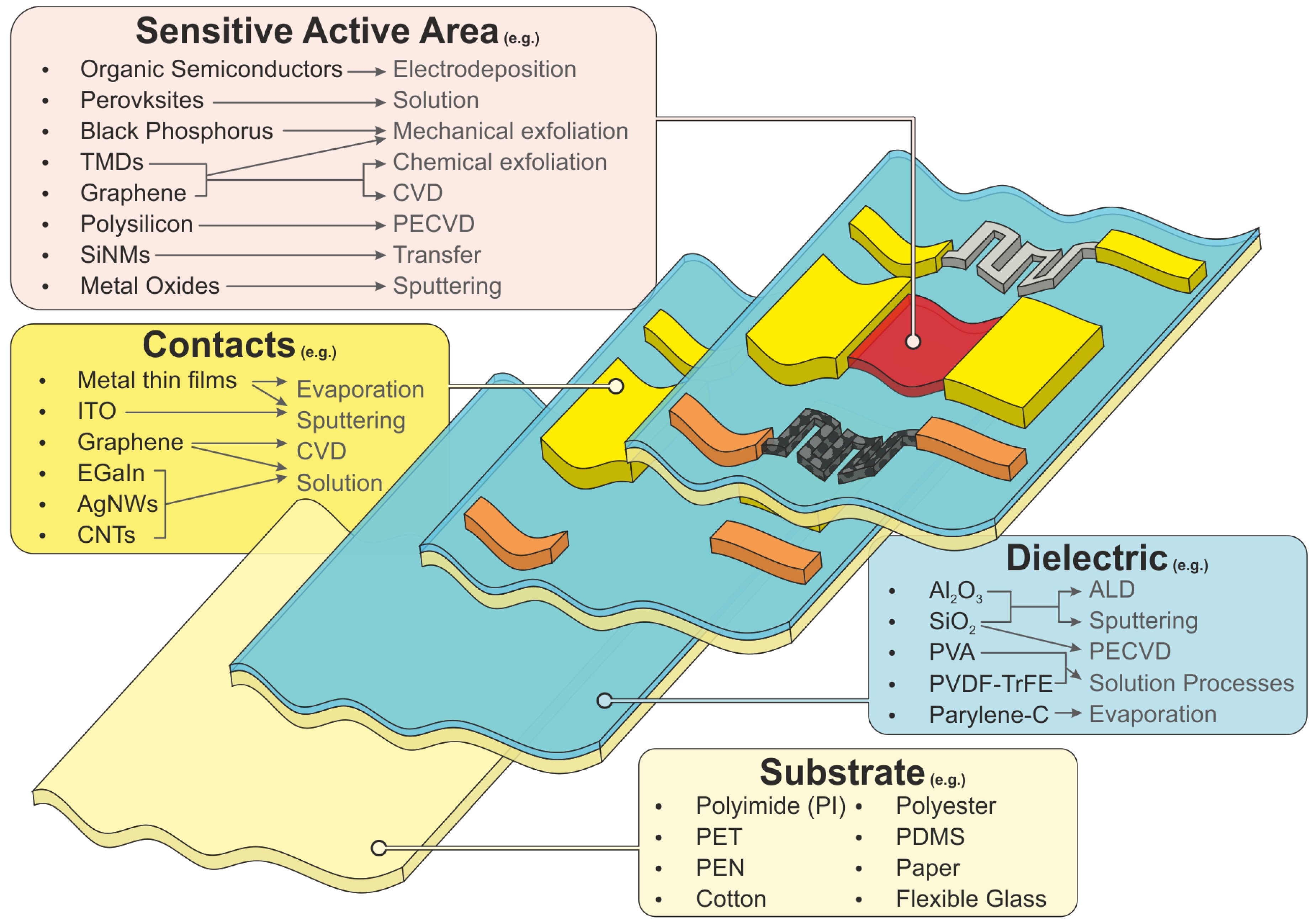
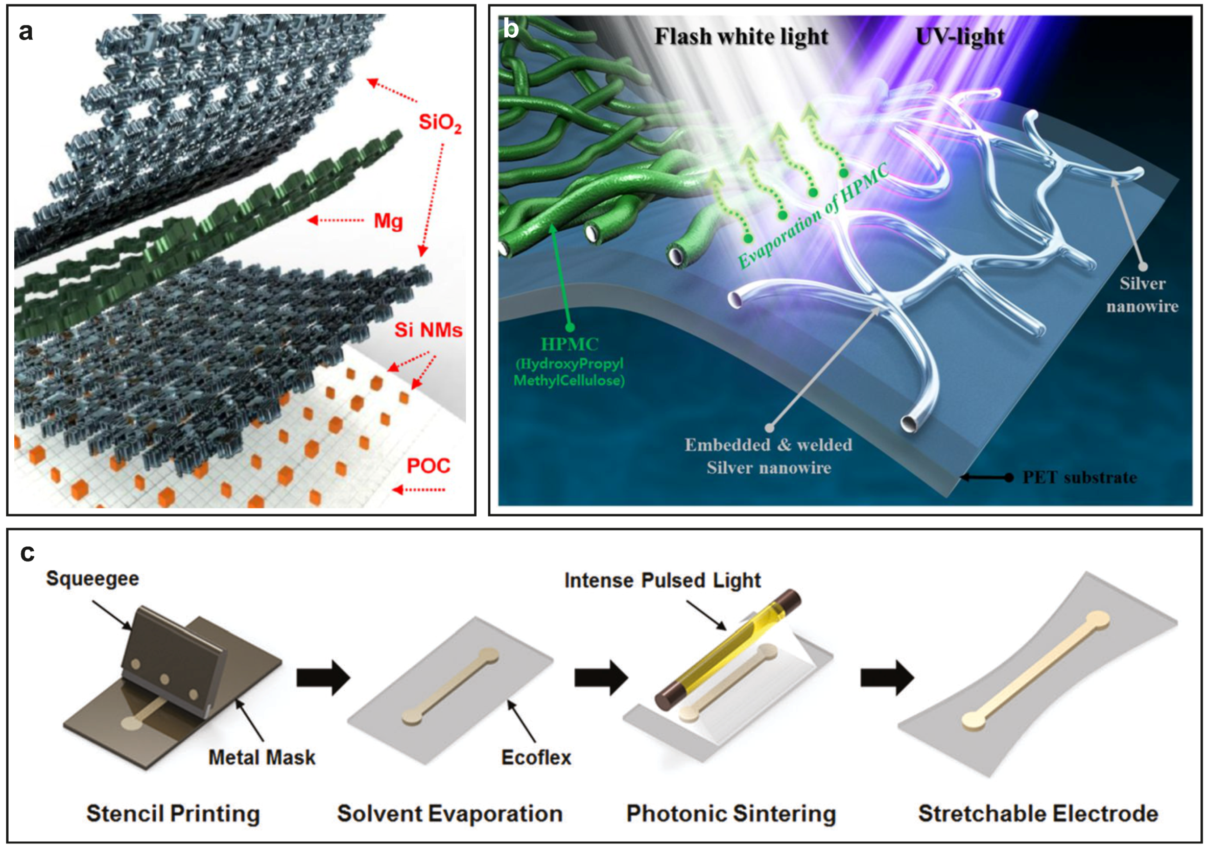
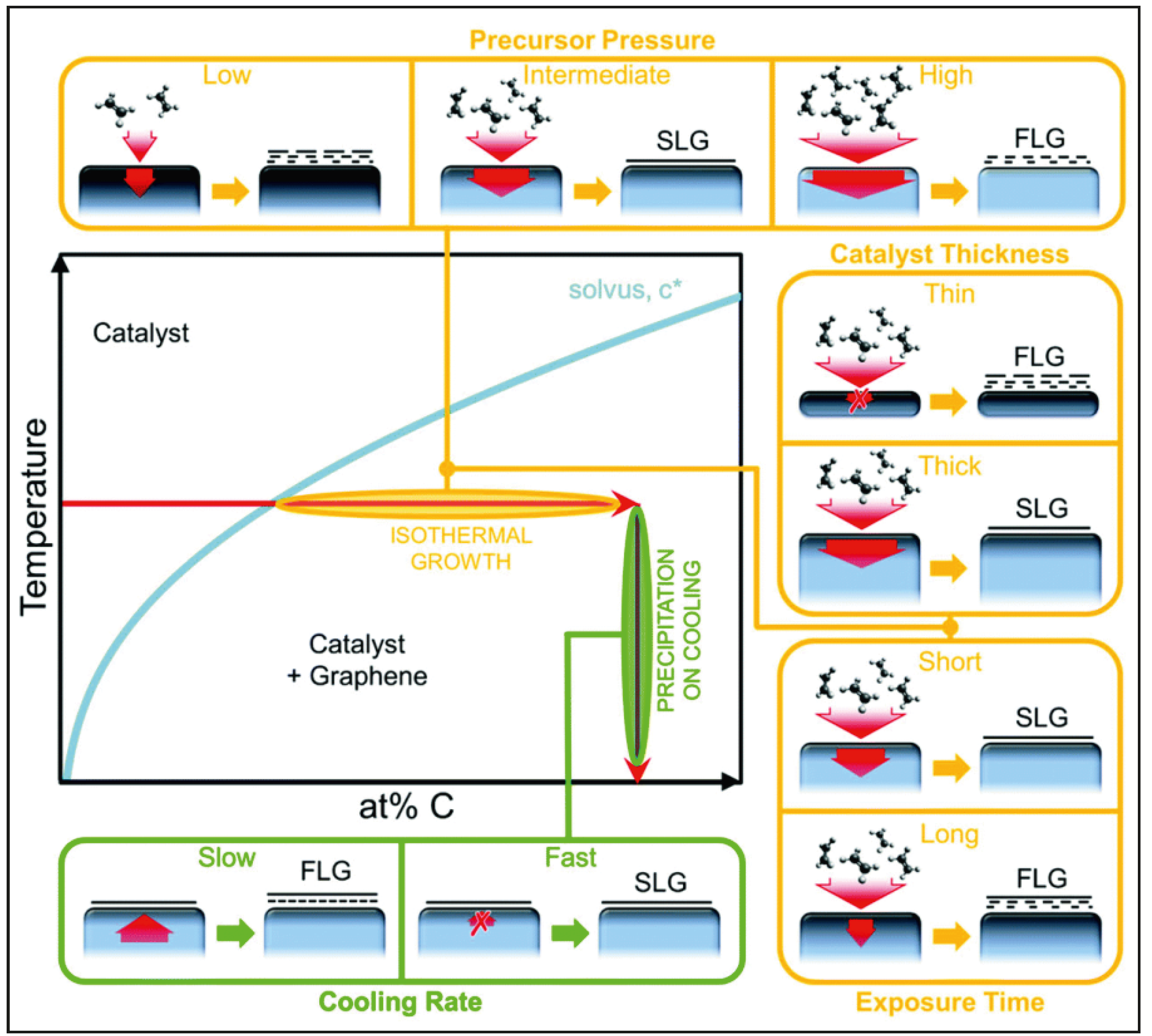
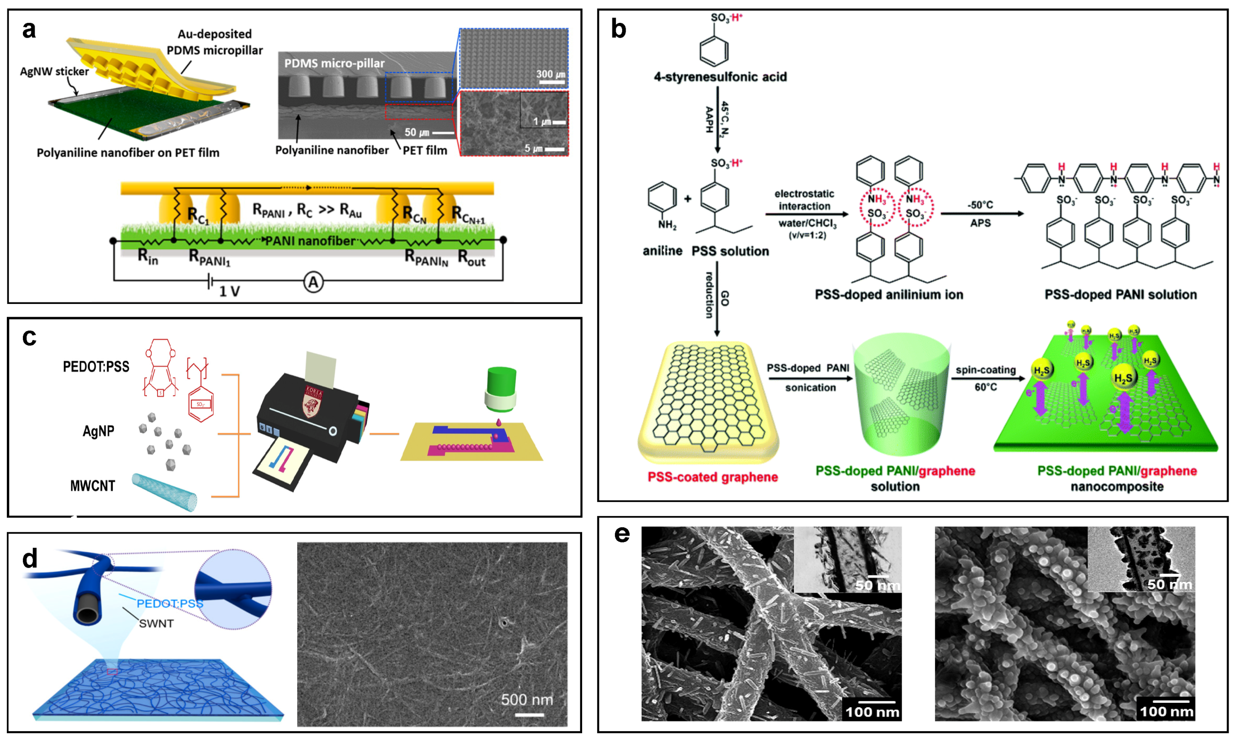
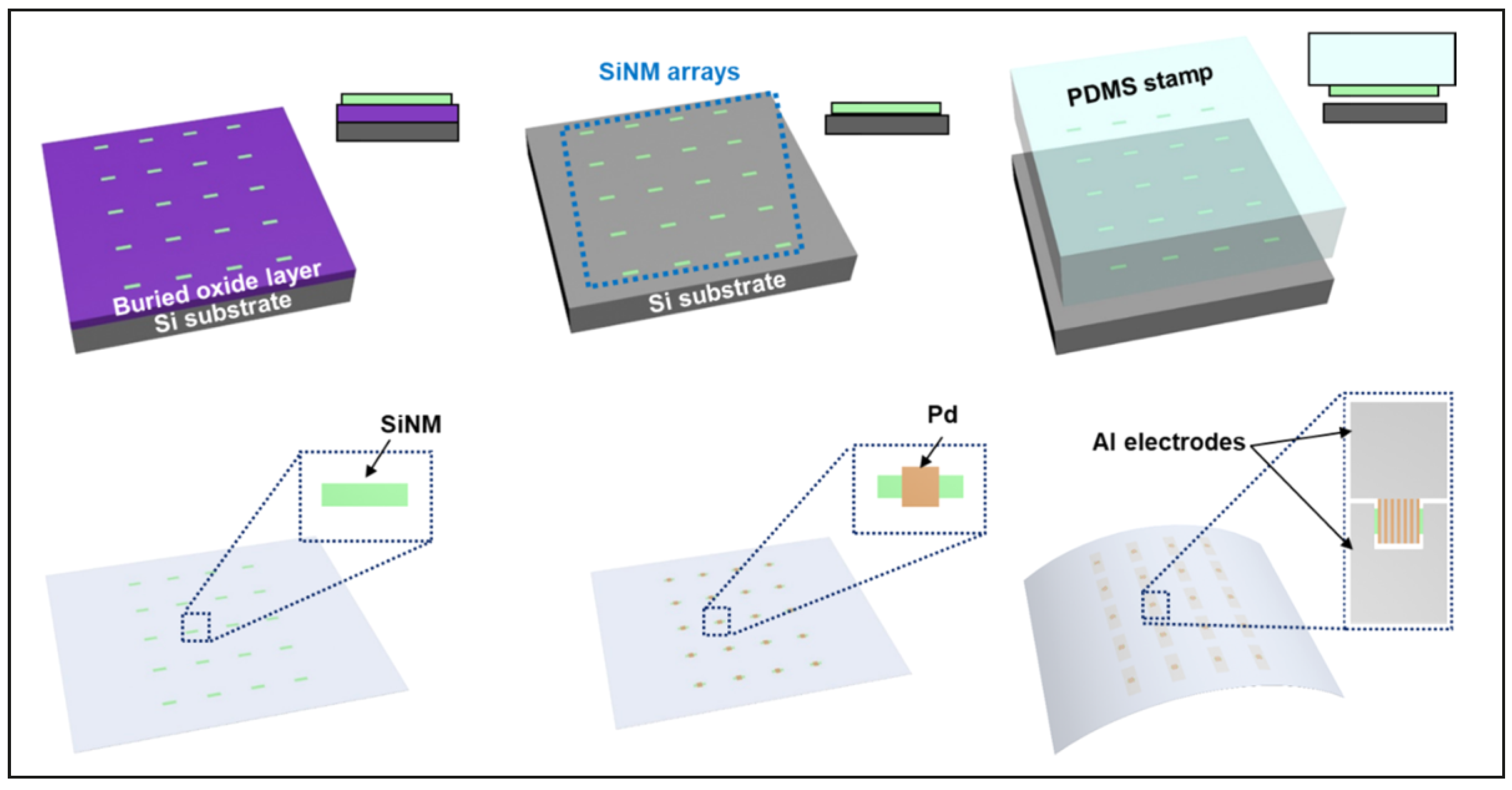
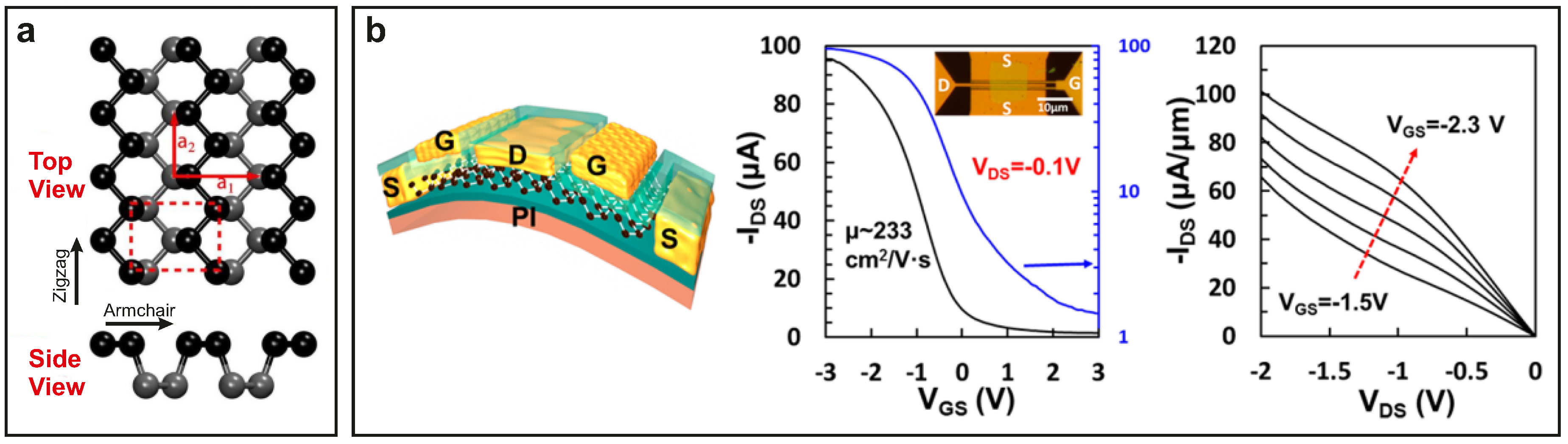
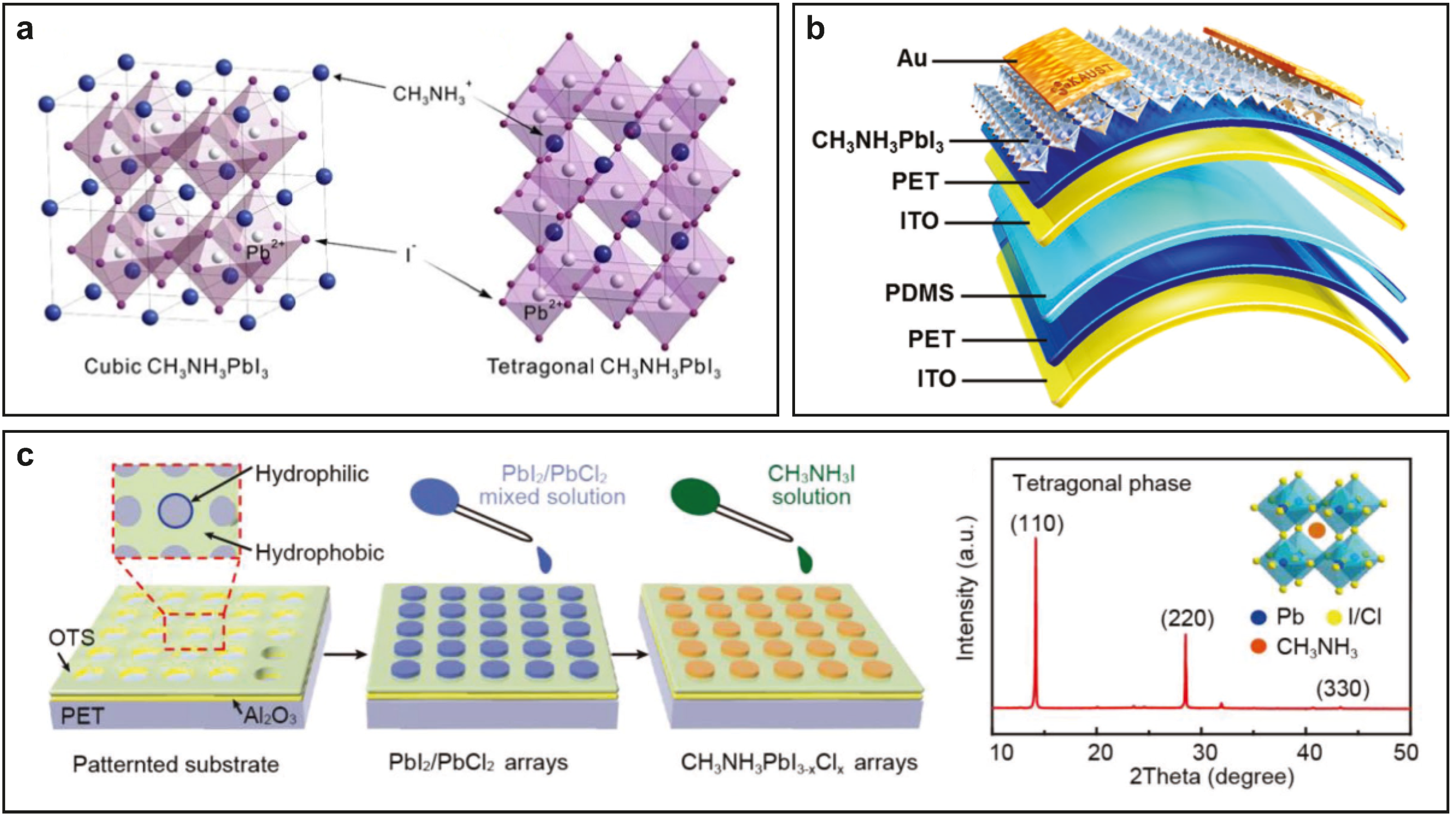
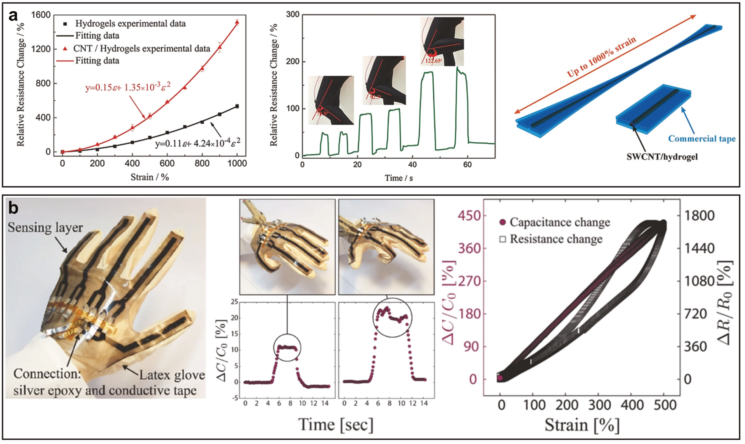
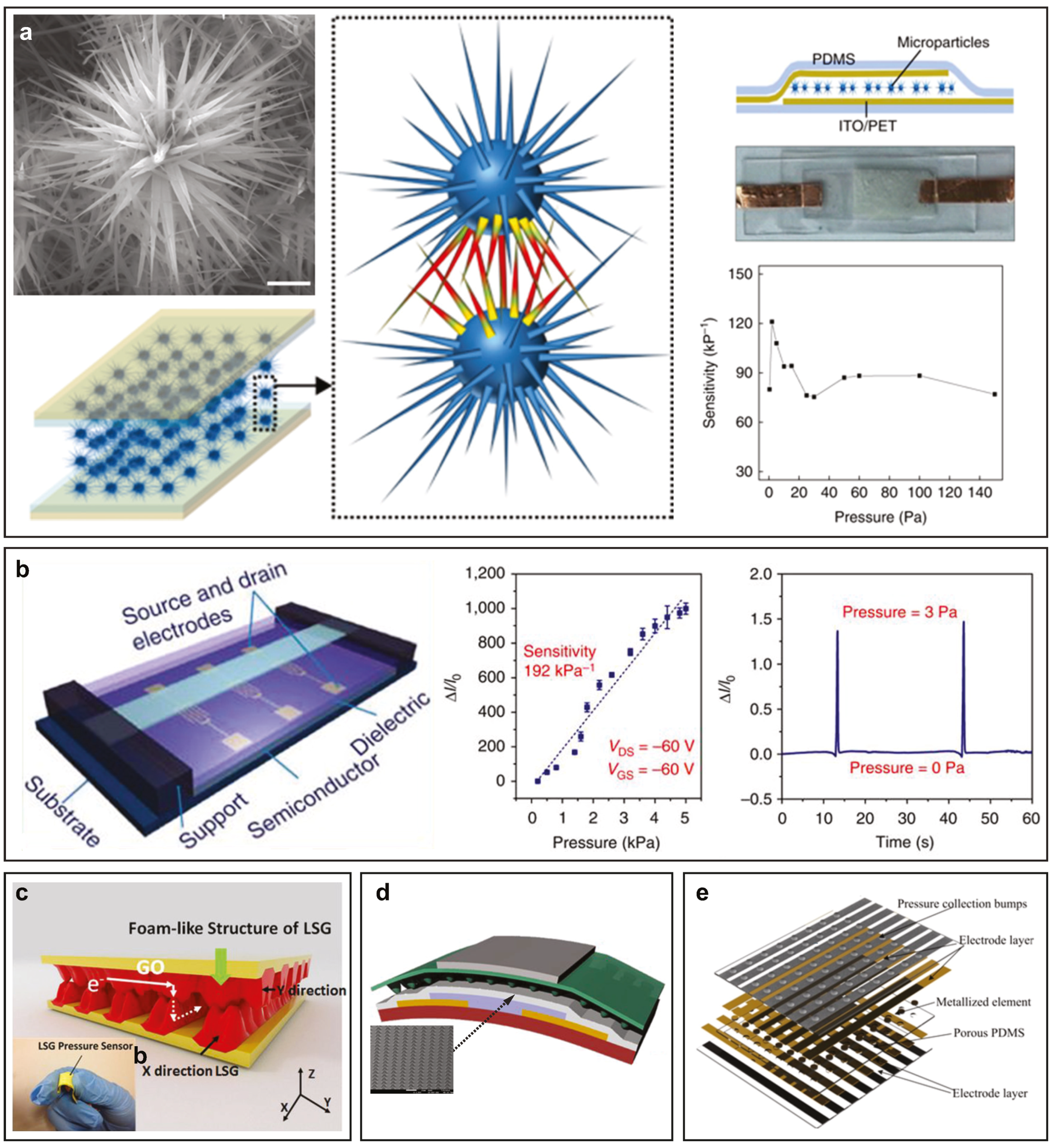
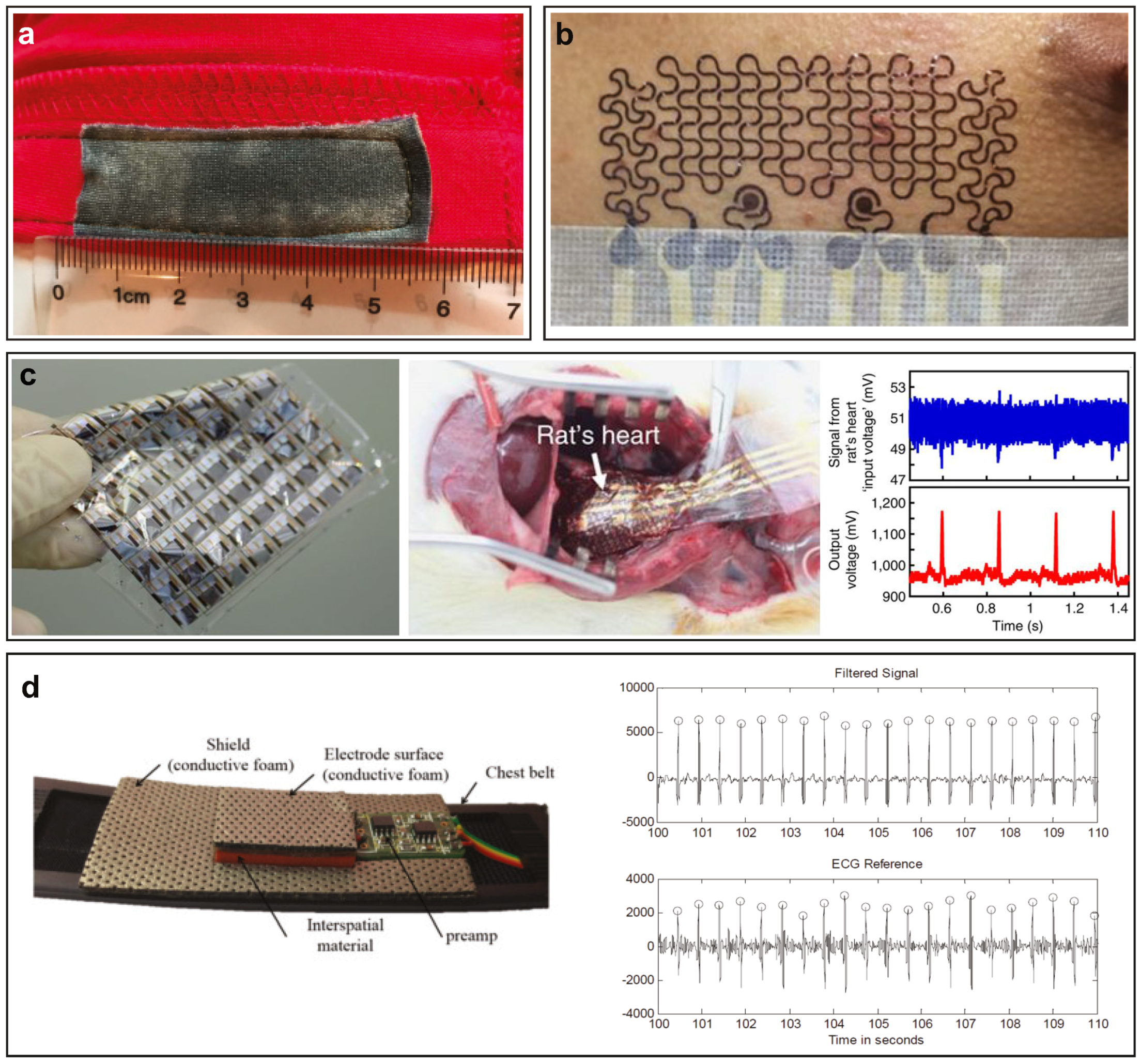
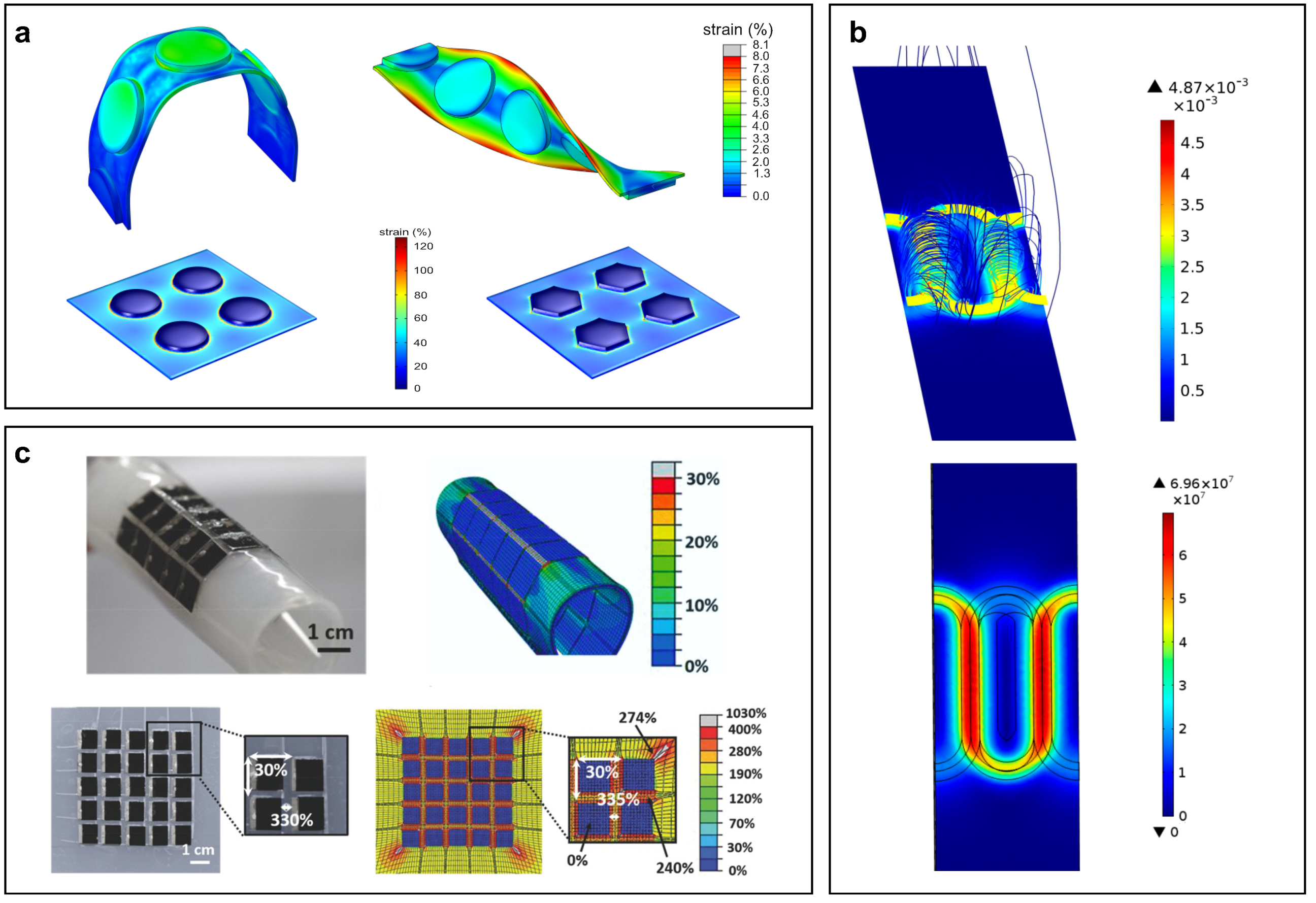
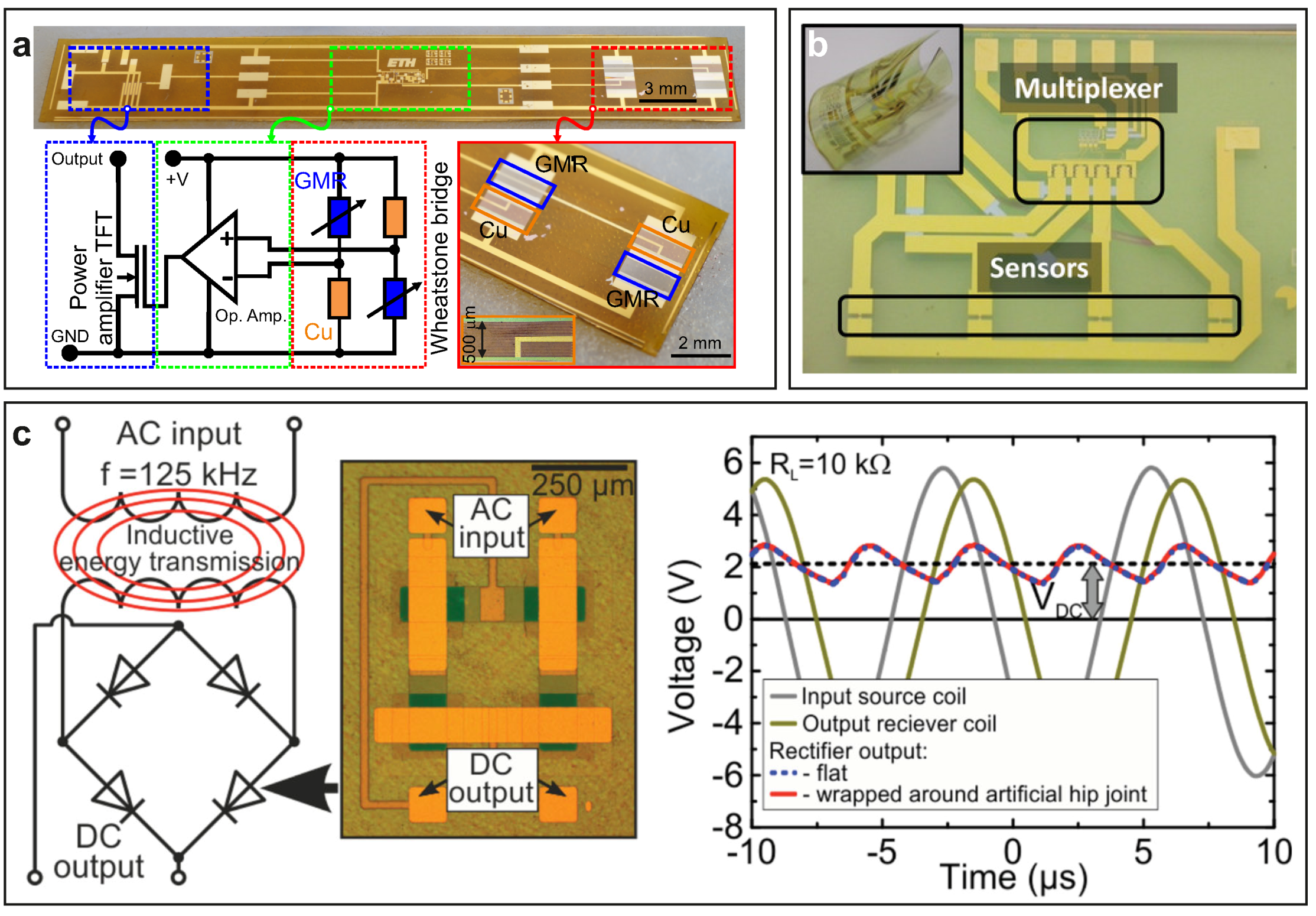
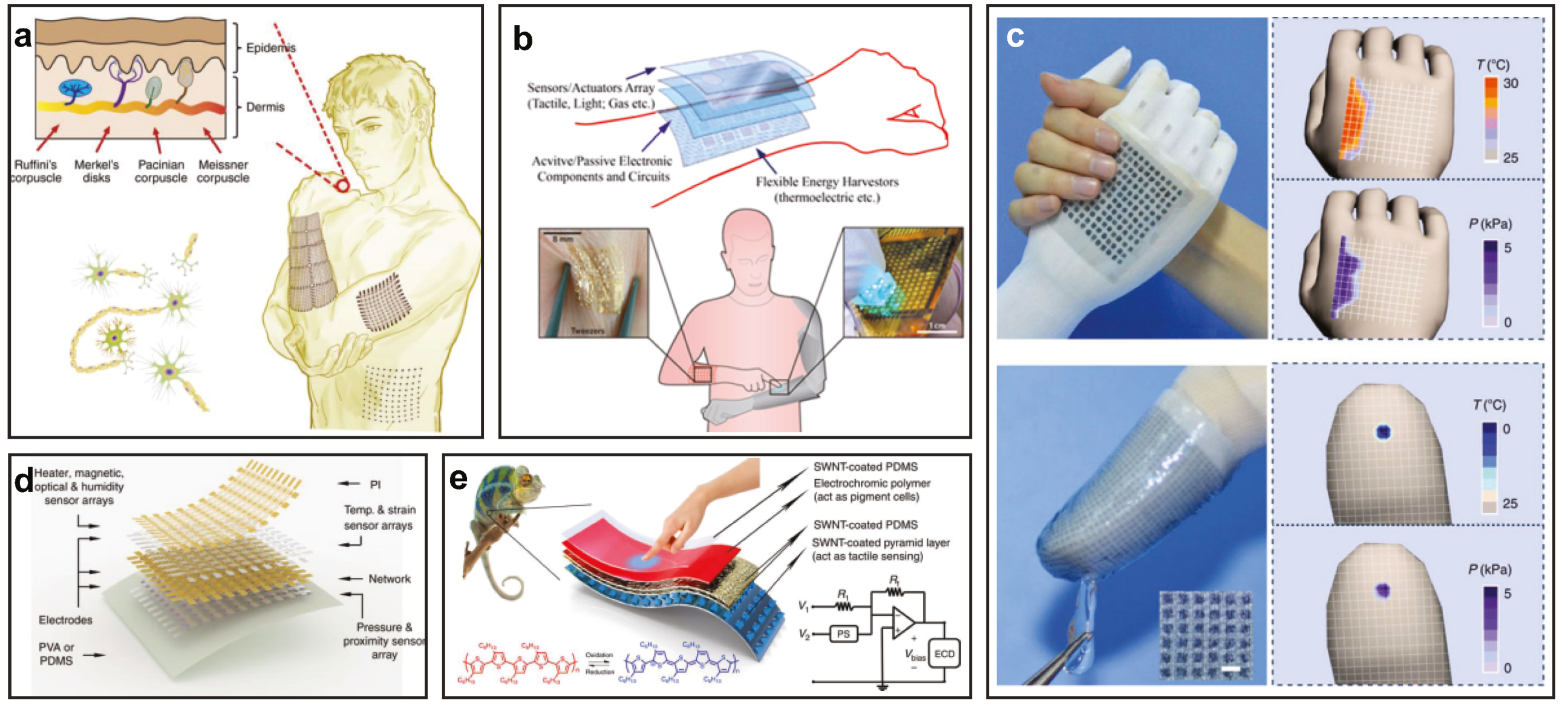
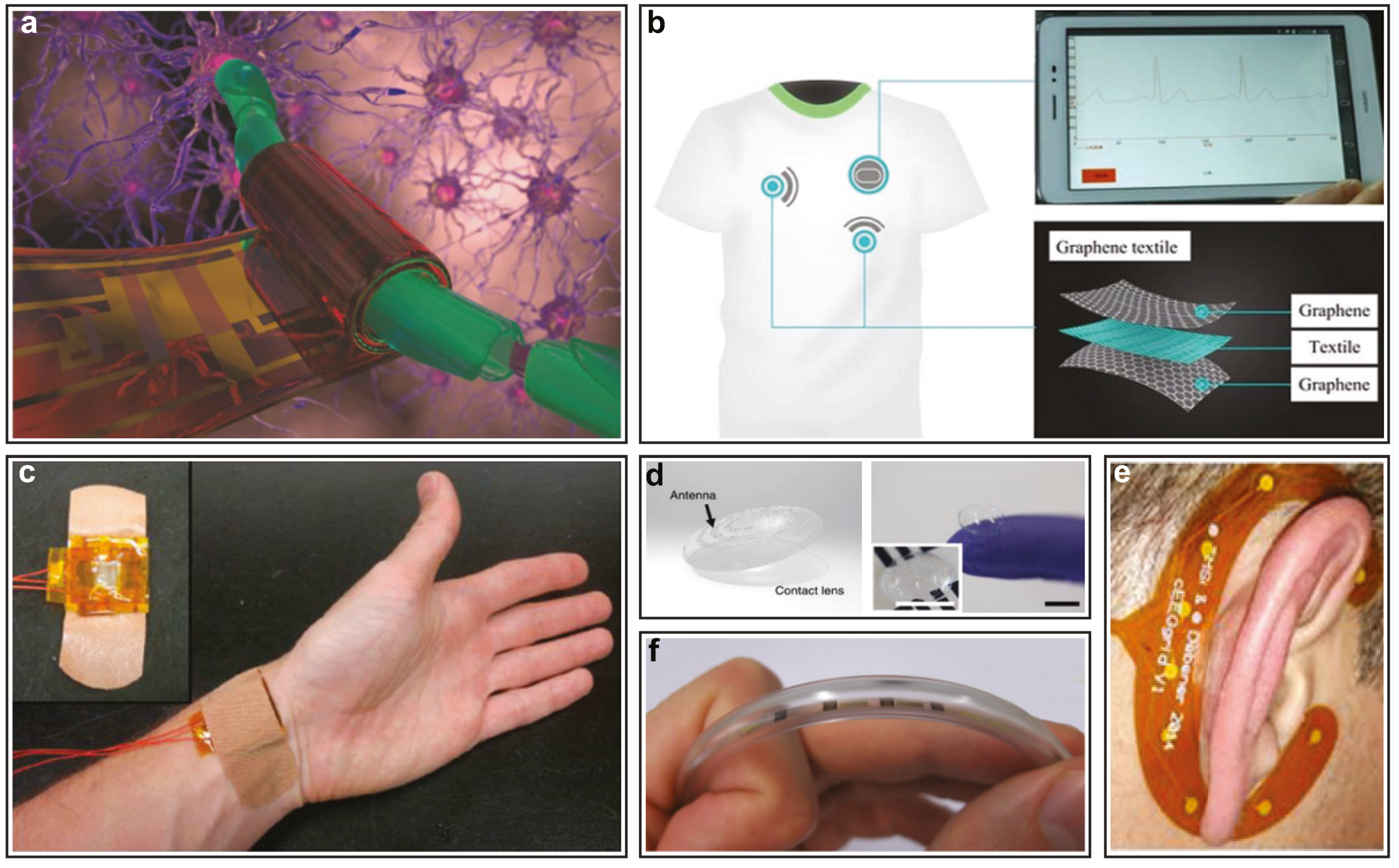
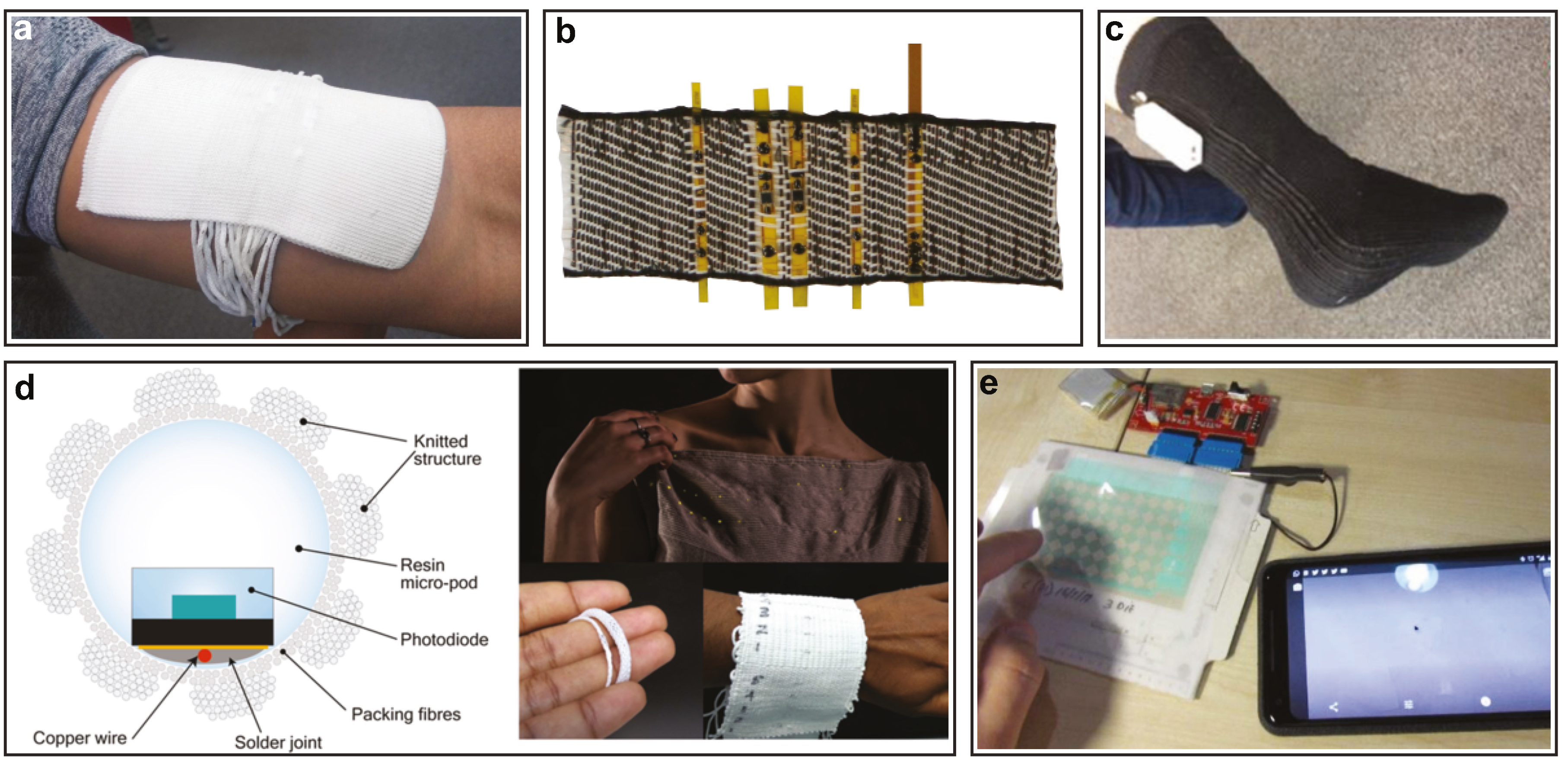
Table 1.
List of flexible strain sensors exhibiting at least one outstanding performance parameter (in bold).
Table 1.
List of flexible strain sensors exhibiting at least one outstanding performance parameter (in bold).
| Material | Type of Sensor | Total Thickness (µm) | Gauge Factor | Stretchability (%) | Response Time (ms) | Hysteresis |
|---|---|---|---|---|---|---|
| Parylene-Ti/Au [366] | Resistive | 1.145 | - | <3 | - | - |
| PDMS-SWCNT-paper [379] | Resistive | 1090 | 50 | 300 | - | |
| Thermoplastic polyurethane-Graphene/Silver Nanoparticles [376] | Resistive | 300 | 7-476 | 1000 | - | - |
| Latex-AuNWs [374] | Resistive | - | 9.9 | >350 | <22 | - |
| Ecoflex™ (00-50)-ethylene glycol and sodium chloride [385] | Resistive | 2000 | <4 | 830 | - | 0.15% (250%) |
Table 2.
List of flexible pressure sensors exhibiting at least one outstanding performance parameter (in bold).
Table 2.
List of flexible pressure sensors exhibiting at least one outstanding performance parameter (in bold).
| Material | Type of Sensor | Total Thickness (µm) | Sensitivity (%\kPa) | Detection Range (Pa) | Response Time (ms) |
|---|---|---|---|---|---|
| Copolymer nanofibres with CNTs and graphene particles on a PET substrate [417] | resistive | 2 | to | 8 to 10,000 | 20 |
| PIDT-BT, PIDT-BT:TCNQ, and P3HT semiconductors with PAA:PEG dielectric [9] | OFET | 176 | 2980 to 45,270 | 200 to 35,000 | 57 |
| PDPP3T semiconductor with a CYTOP protective dielectric layer [10] | SGOTFT | ≈55 | 19,200 | 0.5 to 5000 | <10 |
| Urchin-shaped ZnO microparticles on a PET/ITO layer [422] | resistive and piezoresistive | ≈254 | 7500 to 12,100 | 0.015 to 10,000 | |
| PVA NWs, PPy and PET/ITO [70] | piezoresistive | ≈170 | 1190 to 22,850 | 2.97 to 10,000 | 66.8 |
Table 3.
List of flexible temperature sensors exhibiting at least one outstanding performance parameter (in bold).
Table 3.
List of flexible temperature sensors exhibiting at least one outstanding performance parameter (in bold).
| Material | Type of Sensor | Total Thick. (µm) | Sensitivity | Temperature Range | Stretch. % | Bend. | Resp. Time | Hyster. |
|---|---|---|---|---|---|---|---|---|
| -Mg--Ecoflex™ [442] | Resistive | %/ | 10 | 10 | - | |||
| Parafilm-PAM%/carrageenan double network hydrogel [450] | Resistive | 1500 | 2.6%/ | 330 | 13 | 4% (150% strain) | ||
| PI-Ni [342] | Resistive | - | %/ | −60 to 180 | - | - | - | - |
| PI-Ti/Au [438] | Resistive | ≈50.1 | / | 30 to 60 | 8 | 300 | - | - |
| SEBS-SWCNT [460] | TFT | 124.2 | −24.2 / | 15 to 55 | 60 | - | - | - |
© 2019 by the authors. Licensee MDPI, Basel, Switzerland. This article is an open access article distributed under the terms and conditions of the Creative Commons Attribution (CC BY) license (http://creativecommons.org/licenses/by/4.0/).
Share and Cite
MDPI and ACS Style
Costa, J.C.; Spina, F.; Lugoda, P.; Garcia-Garcia, L.; Roggen, D.; Münzenrieder, N. Flexible Sensors—From Materials to Applications. Technologies 2019, 7, 35. https://doi.org/10.3390/technologies7020035
AMA Style
Costa JC, Spina F, Lugoda P, Garcia-Garcia L, Roggen D, Münzenrieder N. Flexible Sensors—From Materials to Applications. Technologies. 2019; 7(2):35. https://doi.org/10.3390/technologies7020035
Chicago/Turabian StyleCosta, Júlio C., Filippo Spina, Pasindu Lugoda, Leonardo Garcia-Garcia, Daniel Roggen, and Niko Münzenrieder. 2019. "Flexible Sensors—From Materials to Applications" Technologies 7, no. 2: 35. https://doi.org/10.3390/technologies7020035
Note that from the first issue of 2016, this journal uses article numbers instead of page numbers. See further details here.