Communication

A Broadband Active Microwave Monolithically Integrated Circuit Balun in Graphene Technology

1
University of Lille—IEMN CNRS UMR8520, Avenue Poincaré, CS 60069, 59652 Villeneuve d’Ascq, France
2
AMO GmbH, Advanced Microelectronic Center Aachen (AMICA), Otto-Blumenthal-Str. 25, 52074 Aachen, Germany
3
Warsaw University of Technology, Koszykowa 75, str., 00-662 Warsaw, Poland
4
Chair of Electronic Devices, RWTH Aachen University, Otto-Blumenthal-Str. 2, 52074 Aachen, Germany
5
IMS Laboratory, CNRS UMR 5218, Université Bordeaux 1, 33400 Talence, France
*
Author to whom correspondence should be addressed.
Appl. Sci. 2020, 10(6), 2183; https://doi.org/10.3390/app10062183
Submission received: 4 December 2019 / Revised: 5 February 2020 / Accepted: 25 February 2020 / Published: 23 March 2020
(This article belongs to the Special Issue Graphene and Graphene-Based Composites for Electronics)

Abstract

:
This paper presents the first graphene radiofrequency (RF) monolithic integrated balun circuit. It is composed of four integrated graphene field effect transistors (GFETs). This innovative active balun concept takes advantage of the GFET ambipolar behavior. It is realized using an advanced silicon carbide (SiC) based bilayer graphene FET technology having RF performances of about 20 GHz. Balun circuit measurement demonstrates its high frequency capability. An upper limit of 6 GHz has been achieved when considering a phase difference lower than 10° and a magnitude of amplitude imbalance less than 0.5 dB. Hence, this circuit topology shows excellent performance with large broadband performance and a functionality of up to one-third of the transit frequency of the transistor.

1. Introduction

Research in graphene electronics has been extensively directed to the development of RF transistors [1,2,3,4,5,6,7,8,9]. Transistors are the basic building blocks of integrated circuits; they determine their maximal operational frequencies and overall performances. Some RF and millimeter wave circuits based on graphene transistors have been reported with a low noise amplifier (LNA) and a mixer working around 10 to 20 GHz [10], ring oscillator [11,12], graphene radio frequency receiver integrated circuit [13], and a 200 GHz integrated resistive subharmonic mixer based on a single chemical vapor deposition (CVD) G-FET [2]. One of the key concepts for circuit design at very high frequency is the use of differential electronic signals [14]. From a circuit design point of view, the differential topologies have very interesting properties, such as providing immunity to common mode noise couplings and crosstalk through the substrate and supply rails. In addition, at millimeter-wave frequencies, the differential topologies alleviate the negative impact of the bonding wire inductance or the flip-chip bump inductance on the gain, the output power, and the stability of amplifiers [14].
To take advantage of the differential topology concept, the device that is required is the balun or splitter circuit that transforms the single-ended signals (unbalanced) into the differential signals (balanced) and vice versa. Thus, the balun is a device that consists of an unbalanced single-ended input port and two balanced output ports. The main figures of merit (FOMs) of the balun are the phase error and the amplitude difference between the output balanced ports. Finally, specifically for the active balun, the gain is also an important FOM. In [15], we proposed two balun architectures based on graphene FET specificities. The basic working principle of these circuits was demonstrated but this demonstration was limited to very low frequencies (<10 MHz). The circuits were tested by adding external elements such as lumped resistors, basic coaxial cables, and DC probes; thus preventing the evaluation of the high frequency figures of merits of the circuits.
In this paper and for the first time, we have designed and fabricated a RF monolithic integrated balun circuit using a SiC bilayer graphene FET technology. Our monolithically integrated balun consists of four transistors, two of them split the single ended signal in two differential signals, the other two act as active loads, their role is to ensure optimal biasing of the first two transistors.
The SiC substrate is well suited for high-frequency applications: it is highly insulating ensuring low losses at high-frequency and has high thermal conductivity, that is advantageous for thermal management. Therefore, graphene on SiC does not require a transfer step that may contaminate the graphene and reduces the device performances. Here we choose graphene bilayer grown by CVD on silicon carbide since this technique produces wafer scale graphene films that cover the whole substrate, and, in our experience, and are more homogenous than the monolayer graphene. Moreover, comparison of monolayer and bilayer GFETs shows that bilayer have better DC and RF characteristics [16]. The first part of the paper describes the technology used and presents the transistor performances. Second, the balun topology and layout are presented together with the measurement results. Finally, the FOMs of the GFET balun are benchmarked and compared to the state of the art conventional baluns designed in silicon, GaAs, and GaN technologies.

2. Materials and Methods

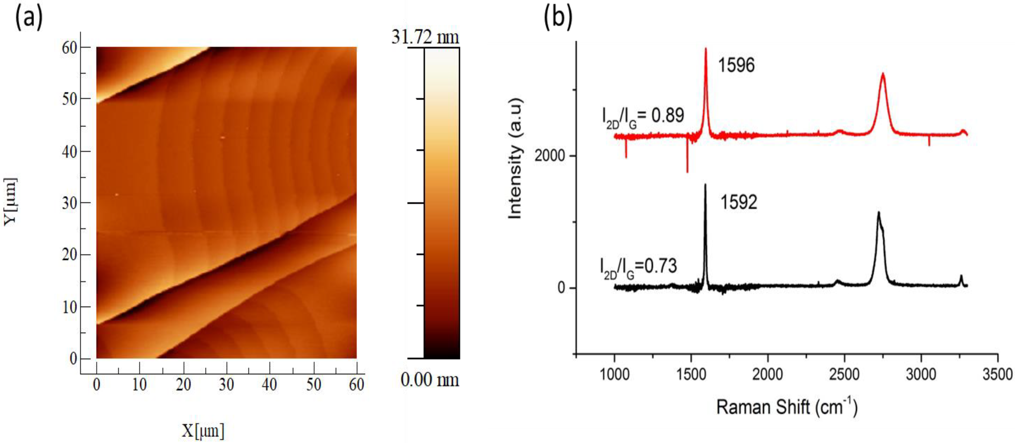
2.1. Graphene Growth and Properties

Epitaxial graphene has been grown by chemical vapor deposition (CVD) on 500 µm thick and high resistivity 6H-SiC (0001) substrate. Commercial horizontal CVD hot wall Aixtron VP508 reactor with RF generator for heating was used. Before the growth, in-situ etching of the SiC surface was carried out in hydrogen atmosphere at 1600 °C with chamber pressure of 100 mbar. The epitaxial carbon films were deposited using propane gas as carbon precursor. The method used is based on high temperature and low argon pressure CVD by creating dynamic conditions of the laminar flow of argon which protect the SiC substrate against Si sublimation and enable mass transport of propane to the SiC surface, thus realizing graphene epitaxy as reported in [17,18,19].
The growth process was followed by in-situ hydrogen intercalation at 1000˚C in 900 mbar Ar atmosphere. The growth parameters were optimized to achieve a bilayer graphene. The initial carrier density and the mobility were extracted from non-contact terahertz spectroscopic measurement and estimated around +8.3 × 1012 cm−2 and 850 cm2.V−1s−1, respectively [20].
Raman spectroscopy was performed using the HORIBA Jobin-Yvon lab system at a laser wavelength of 473 nm, using 1 µm laser spot size and filters to deliver power less than 0.1 mW and ×100 objective lens to measure different position of the sample.

2.2. Circuit Fabrication

Monolithically integrated balun circuits containing four graphene field effect transistors each were fabricated on a 15 × 15 mm2 SiC wafer. First, we define the alignment marks. Then we etch the graphene channel and holes in the contacts region for improving contact resistance, as reported previously [21,22]. The source and drain contacts are patterned using the e-beam lithography (EBL) followed by deposition of 1.5 nm of nickel and 30 nm of gold and lift-off process. Here the 1.5 nm thin layer of nickel is used to improve the metal adhesion on the surface. Then, dual T-gate with gate length (Lg) were defined by EBL using a three layers poly-meta-methacrylate resist. After the development of the multilayers’ resist, the gate oxide was obtained by depositing four times 2 nm of aluminum, following by oxidation in ambient air during 24 h. Finally, the coplanar access and interconnections between transistors were fabricated (Ni/Au 50 nm/300 nm).

3. Results

We first discuss the graphene material used in this work. Figure 1a presents the atomic force microscopy (AFM) image of 60 × 60 µm2 graphene surface on SiC. It shows the presence of SiC steps which are several tens of µm wide. Two typical Raman spectra measured on the sample are illustrated on Figure 1b, after subtraction of the Raman signal coming from the SiC. The G and 2D peaks, a characteristic feature of graphene, are clearly visible (with G peak at 1596 cm−1 and 1592 cm−1) [23]. The D peak intensity is either not detected or much smaller than our G peak, indicating that structural defects are absent or present in very small a mount [24]. The width of 2D peak and the low value of the ratio I2D/IG < 1 indicates that the graphene is mainly a bilayer.

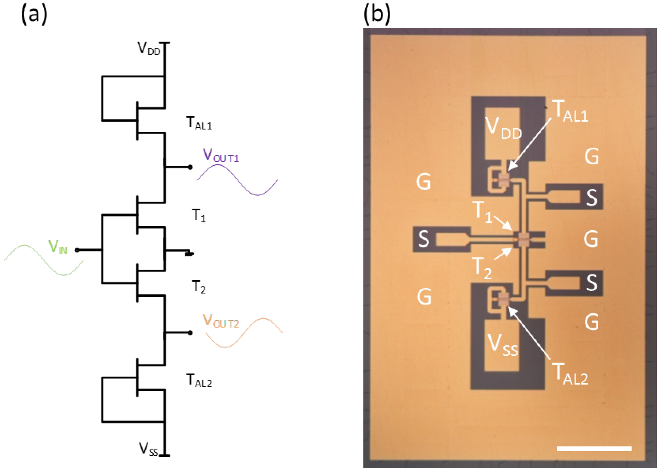
3.1. Circuit Description

The fabricated circuit is presented in Figure 2. The GFET-Balun is realized using two active GFET transistors (T1 and T2) where the sources are connected together and two loads (transistors TAL1 and TAL2) that are tied to the drains of T1 and T2 and connected to the power supplies VDD and VSS, respectively (see Figure 2b). In comparison to [15], lumped resistors are replaced by integrated active loads using transistors where the gate is connected to the source. The input signal is applied to the gates of T1 and T2 (both gates are connected together). The gate-source voltage of the graphene transistors is hence equal to VGS0 + Vac, where VGS0 is the DC-offset voltage used for accurately setting the quiescent point. The balanced output signals are measured at the drains. The circuit has been simulated with the compact model described in [25,26] and also applying a mixed SPICE and electromagnetic simulation through ADS-Momentum. In the previous graphene simulated circuit [26] and considering the former available technology developed at University of Lille [15], circuit shows performances in the GHz range with a difference of phase lower than 10° up to 1.2 GHz.

3.2. GFET Description

The transistor channel is composed of a bilayer graphene. The gate length is about 240 nm. A top gate is used with an insulator thickness of about 15 nm made of Al2O3. The channel width of each device is 24 µm. The DC ID-VGS and its associated transconductance characteristics of a GFET, as well as the AC-characteristics were measured on a transistor situated at close proximity of the balun for minimal dispersion. The influence of the pads has been removed through appropriated test-structures and de-embedding. Maximum transconductance is about 5 mS. The gate-source capacitance CGS is about 26fF while the gate-drain capacitance CGD is about 8fF. The device is characterized by a cut-off frequency of 19 GHz and a maximum oscillation frequency of 6 GHz.

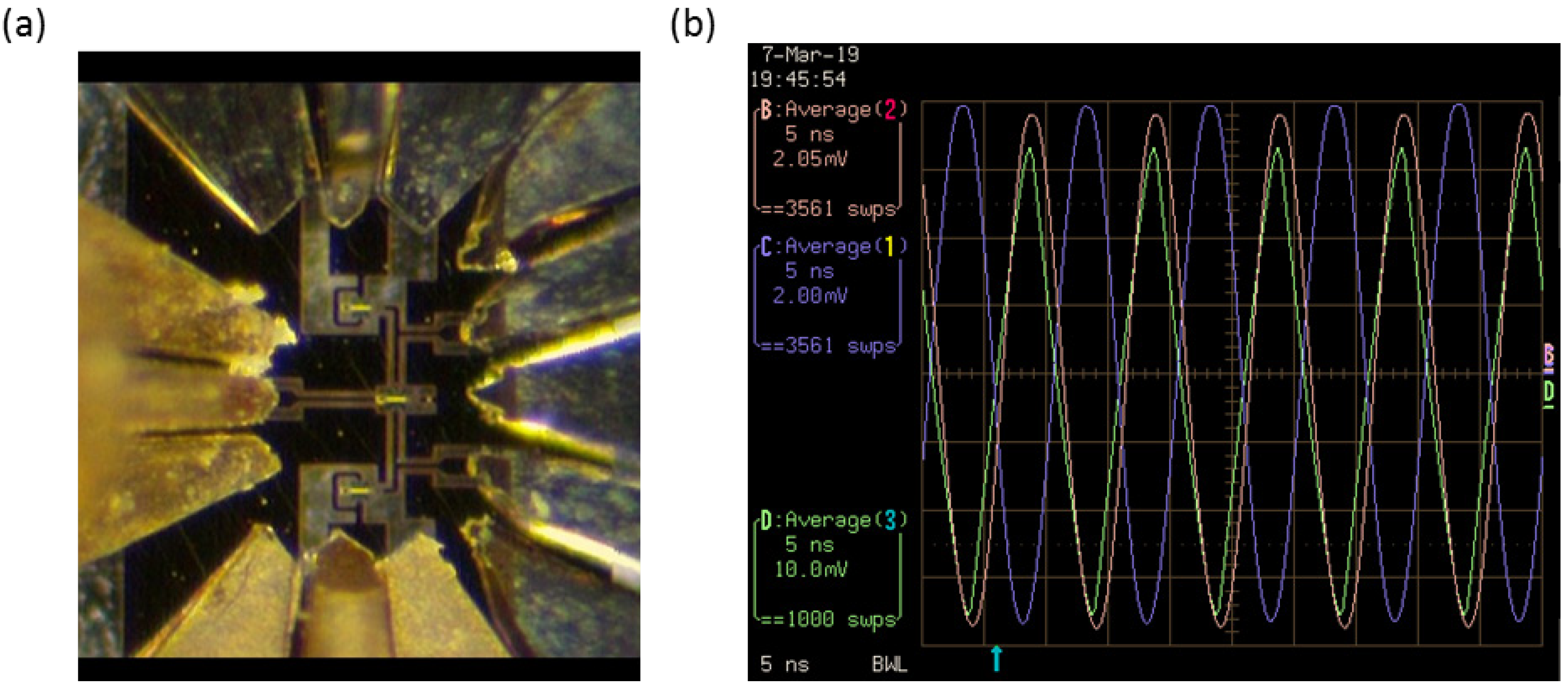
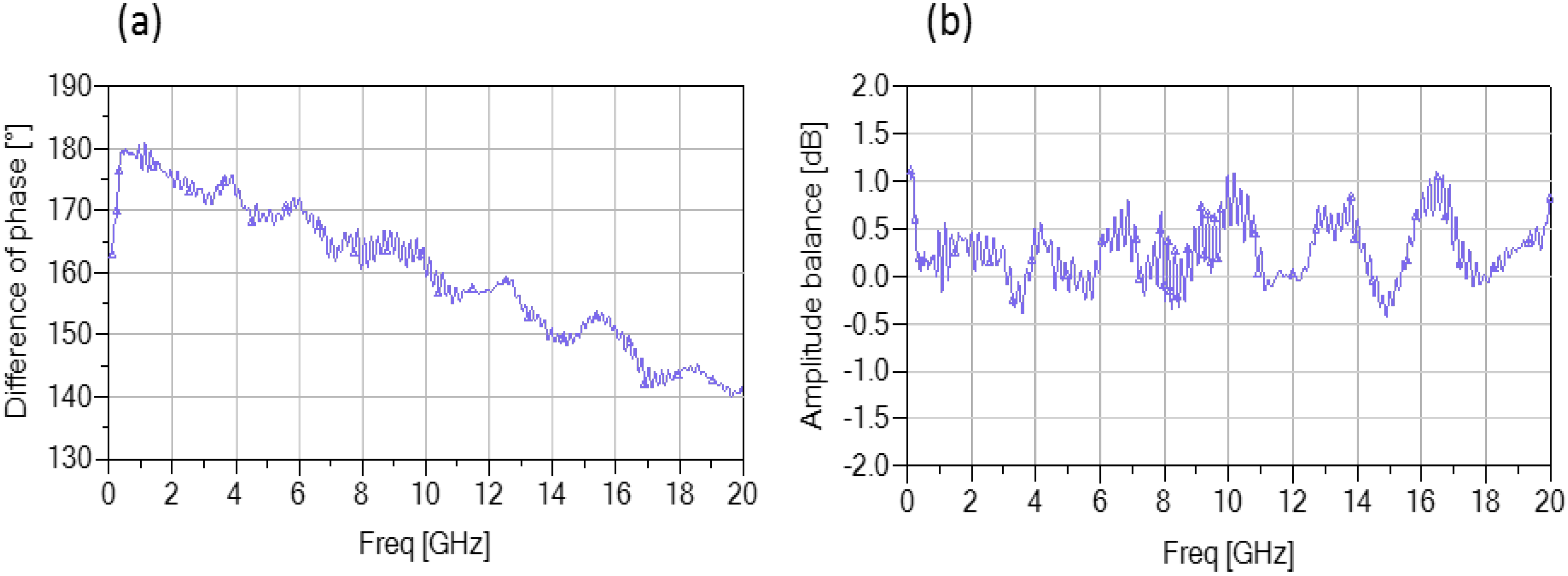
3.3. Balun Circuit Characterization

First functionality tests have been performed thanks to time domain measurement using a RF source set at 100 MHz and −10 dBm. One single RF probes is used at the input while a differential probe is used at the output.
Two other RF probes are used for convenience to apply the DC bias. +2 V and −2 V are applied on VDD and VSS, respectively. Also, +2 V is applied on the input thanks to a bias tee. A photography of the balun under measurement conditions is shown in Figure 3a.
Scope measurements are presented in Figure 3b, highlighting the functionality of the circuit with 180° phase shift between the two outputs. In that first measurement setup, the measurement is not calibrated and does not allow high-frequency measurement. In the following, we discuss high-frequency measurements carried out with a 4-port PNAX vector network analyzer (VNA) which can obtain calibrated data at the probe level. In order to perform the differential measurement with the VNA, the intermediate frequency is set to 100 Hz and the input power is fixed to −10 dBm.
The setup is calibrated using a calibration kit dedicated to differential probes. Measurements reveal that the two output signals have a phase difference of 180° up to the GHz range (see Figure 4a). This difference decreases to 170° at 6 GHz. The output signals are attenuated of about 20 dB with an amplitude imbalance lower than 0.5 dB below 6 GHz (see Figure 4b). The bias current is 40 mA giving a power consumption of 160 mW. The strong attenuation of 20 dB is directly correlated to the transistors’ performances and especially to the high output conductance gDS, a specific weakness of graphene devices. Also, the power consumption can be optimized by reducing gate width to obtain the optimal tradeoff between power consumption and output impedance of the balun.

4. Discussion

Comparison with State of the Art

Finally, the balun circuit is compared to the state of the art of active baluns made with different technologies such as silicon [27], SiGe [28], GaAs [29], and GaN [30] (Table 1). These publications are chosen to have a similar technology gate length than the graphene technology used in this paper ranging from 0.18 to 0.5 µm. The transit frequencies of these technologies are also in the same range spanning from about 20 and up to 40 GHz. Moreover, the baluns are designed for broadband applications below 16 GHz. The graphene balun presented in this work have comparable performance in terms of phase difference and amplitude balance compared to the industrial technology despites its low maturity. As mentioned early, the major drawback is due to the losses in the graphene balun which is intrinsically correlated to the transistor performances and not to the circuit topology itself.

5. Conclusions

A graphene-based broadband balun monolithically integrated circuit working up to 6 GHz has been demonstrated for the first time. Our integrated balun is based on SiC graphene bilayer technology and contains four individual transistors. The graphene-based balun performances are compared to state of the art baluns on semiconducting technologies having similar RF-characteristics. This comparison accounts for frequency bandwidth, phase difference, amplitude balance, and die area. Comparable performances are achieved except for the gain. The circuit performances are intrinsically correlated to the transistor performances: for the graphene-based topology, the circuit works up to one-third of the transistor’s transit frequency which is suitable for the new 5G NR sub-6 standard.
The balun concept based on the ambipolar behavior of the GFET that has been presented in this paper may be replicated on other promising materials such as TMDs materials, carbon nanotube FETs or other ambipolar FETs.

Author Contributions

Investigation, D.F., V.P., W.W., S.B.S., W.S., M.C.L., T.Z., E.P., H.H. and S.F.; Methodology, D.Z.; Writing—S.F, E.P original draft, all authors contributed to the final version of the manuscript. All authors have read and agreed to the published version of the manuscript.

Funding

This research was funded by Horizon 2020 Framework Program: Core2 785219.

Acknowledgments

The authors acknowledge funding through the EU Horizon2020 research and innovation program (Graphene Flagship—Graphene Core2 785219). This work was partially supported by the French RENATECH network.

Conflicts of Interest

The authors declare no conflict of interest.

References

  1. Fadil, D.; Wei, W.; Deng, M.; Fregonese, S.; Strupinski, W.; Pallecchi, E.; Happy, H. 2D-Graphene Epitaxy on SiC for RF Application: Fabrication, Electrical Characterization and Noise Performance. In Proceedings of the 2018 IEEE/MTT-S International Microwave Symposium—IMS, Philadelphia, PA, USA, 10–15 June 2018; pp. 228–231. [Google Scholar]
  2. Fadil, D.; Wei, W.; Pallecchi, E.; Anderson, M.; Stake, J.; Deng, M.; Fregonese, S.; Zimmer, T.; Happy, H. 2D RF Electronics: From Devices to Circuits-Challenges and Applications. In Proceedings of the 2018 76th Device Research Conference (DRC), Santa Barbara, CA, USA, 24–27 June 2018; pp. 1–2. [Google Scholar]
  3. Sang, L.; Xu, Y.; Wu, Y.; Chen, R. Device and Compact Circuit-Level Modeling of Graphene Field-Effect Transistors for RF and Microwave Applications. IEEE Trans. Circuits Syst. I Regul. Pap. 2018, 65, 2559–2570. [Google Scholar] [CrossRef]
  4. Wang, Z.; Zhang, Q.; Wei, Z.; Peng, P.; Tian, Z.; Ren, L.; Zhang, X.; Huang, R.; Wen, J.; Fu, Y. Stability of radio-frequency graphene field-effect transistors in ambient. J. Phys. D Appl. Phys. 2018, 52, 055101. [Google Scholar] [CrossRef]
  5. Pandey, H.; Shaygan, M.; Sawallich, S.; Kataria, S.; Wang, Z.; Noculak, A.; Otto, M.; Nagel, M.; Negra, R.; Neumaier, D.; et al. All CVD Boron Nitride Encapsulated Graphene FETs with CMOS Compatible Metal Edge Contacts. IEEE Trans. Electron Devices 2018, 65, 4129–4134. [Google Scholar] [CrossRef] [Green Version]
  6. Das, T.; Sharma, B.K.; Katiyar, A.K.; Ahn, J.-H. Graphene-based flexible and wearable electronics. J. Semicond. 2018, 39, 011007. [Google Scholar] [CrossRef]
  7. Yang, W.; Berthou, S.; Lu, X.; Wilmart, Q.; Denis, A.; Rosticher, M.; Taniguchi, T.; Watanabe, K.; Fève, G.; Berroir, J.-M.; et al. A graphene Zener–Klein transistor cooled by a hyperbolic substrate. Nat. Nanotechnol. 2018, 13, 47–52. [Google Scholar] [CrossRef] [PubMed] [Green Version]
  8. Wei, W.; Pallecchi, E.; Haque, S.; Borini, S.; Avramovic, V.; Centeno, A.; Amaia, Z.; Happy, H. Mechanically robust 39 GHz cut-off frequency graphene field effect transistors on flexible substrates. Nanoscale 2016, 8, 14097–14103. [Google Scholar] [CrossRef] [PubMed]
  9. Montanaro, A.; Wei, W.; De Fazio, D.; Sassi, U.; Soavi, G.; Ferrari, A.C.; Happy, H.; Legagneux, P.; Pallecchi, E. Optoelectronic mixing with high frequency graphene transistors. arXiv 2019, arXiv:1905.09967. [Google Scholar]
  10. Yeh, C.-H.; Lain, Y.-W.; Chiu, Y.-C.; Liao, C.-H.; Moyano, D.R.; Hsu, S.S.H.; Chiu, P.-W. Gigahertz Flexible Graphene Transistors for Microwave Integrated Circuits. ACS Nano 2014, 8, 7663–7670. [Google Scholar] [CrossRef]
  11. Schall, D.; Otto, M.; Neumaier, D.; Kurz, H. Integrated Ring Oscillators based on high-performance Graphene Inverters. Sci. Rep. 2013, 3, 2592. [Google Scholar] [CrossRef]
  12. Guerriero, E.; Polloni, L.; Bianchi, M.; Behnam, A.; Carrion, E.; Rizzi, L.G.; Pop, E.; Sordan, R. Gigahertz Integrated Graphene Ring Oscillators. ACS Nano 2013, 7, 5588–5594. [Google Scholar] [CrossRef]
  13. Han, S.-J.; Garcia, A.V.; Oida, S.; Jenkins, K.A.; Haensch, W. Graphene radio frequency receiver integrated circuit. Nat. Commun. 2014, 5, 3086. [Google Scholar] [CrossRef] [PubMed]
  14. Voinigescu, S. High-Frequency Integrated Circuits. Available online: https://www.biblio.com/high-frequency-integrated-by-voinigescu-sorin/work/3673096 (accessed on 20 March 2019).
  15. Zimmer, T.; Frégonèse, S. Graphene Transistor-Based Active Balun Architectures. IEEE Trans. Electron Devices 2015, 62, 3079–3083. [Google Scholar] [CrossRef]
  16. He, Z.-Z.; Yang, K.-W.; Yu, C.; Liu, Q.-B.; Wang, J.-J.; Song, X.-B.; Han, T.-T.; Feng, Z.-H.; Cai, S.-J. Comparative Study of Monolayer and Bilayer Epitaxial Graphene Field-Effect Transistors on SiC Substrates. Chin. Phys. Lett. 2016, 33, 086801. [Google Scholar] [CrossRef]
  17. Strupinski, W.; Grodecki, K.; Wysmolek, A.; Stepniewski, R.; Szkopek, T.; Gaskell, P.E.; Grüneis, A.; Haberer, D.; Bozek, R.; Krupka, J.; et al. Graphene Epitaxy by Chemical Vapor Deposition on SiC. Nano Lett. 2011, 11, 1786–1791. [Google Scholar] [CrossRef] [PubMed]
  18. Ciuk, T.; Cakmakyapan, S.; Ozbay, E.; Caban, P.; Grodecki, K.; Krajewska, A.; Pasternak, I.; Szmidt, J.; Strupinski, W. Step-edge-induced resistance anisotropy in quasi-free-standing bilayer chemical vapor deposition graphene on SiC. J. Appl. Phys. 2014, 116, 123708. [Google Scholar] [CrossRef] [Green Version]
  19. Ciuk, T.; Caban, P.; Strupinski, W. Charge carrier concentration and offset voltage in quasi-free-standing monolayer chemical vapor deposition graphene on SiC. Carbon 2016, 101, 431–438. [Google Scholar] [CrossRef]
  20. Buron, J.D.; Pizzocchero, F.; Jepsen, P.U.; Petersen, D.H.; Caridad, J.M.; Jessen, B.S.; Booth, T.J.; Bøggild, P. Graphene mobility mapping. Sci. Rep. 2015, 5, 12305. [Google Scholar] [CrossRef] [Green Version]
  21. Passi, V.; Gahoi, A.; Ruhkopf, J.; Kataria, S.; Vaurette, F.; Pallecchi, E.; Happy, H.; Lemme, M.C. Contact Resistance Study of “Edge-Contacted” Metal-Graphene Interfaces. In Proceedings of the 2016 46th European Solid-State Device Research Conference (ESSDERC), Lausanne, Switzerland, 12–15 September 2016; pp. 236–239. [Google Scholar]
  22. Anzi, L.; Mansouri, A.; Pedrinazzi, P.; Guerriero, E.; Fiocco, M.; Pesquera, A.; Centeno, A.; Zurutuza, A.; Behnam, A.; Carrion, E.A.; et al. Ultra-low contact resistance in graphene devices at the Dirac point. 2D Mater. 2018, 5, 025014. [Google Scholar] [CrossRef]
  23. Ferrari, A.C.; Meyer, J.C.; Scardaci, V.; Casiraghi, C.; Lazzeri, M.; Mauri, F.; Piscanec, S.; Jiang, D.; Novoselov, K.S.; Roth, S.; et al. Raman Spectrum of Graphene and Graphene Layers. Phys. Rev. Lett. 2006, 97, 187401. [Google Scholar] [CrossRef] [Green Version]
  24. Ferrari, A.C.; Robertson, J. Interpretation of Raman spectra of disordered and amorphous carbon. Phys. Rev. B 2000, 61, 14095–14107. [Google Scholar] [CrossRef] [Green Version]
  25. Frégonèse, S.; Magallo, M.; Maneux, C.; Happy, H.; Zimmer, T. Scalable Electrical Compact Modeling for Graphene FET Transistors. IEEE Trans. Nanotechnol. 2013, 12, 539–546. [Google Scholar] [CrossRef]
  26. Aguirre-Morales, J.; Frégonèse, S.; Mukherjee, C.; Wei, W.; Happy, H.; Maneux, C.; Zimmer, T. A Large-Signal Monolayer Graphene Field-Effect Transistor Compact Model for RF-Circuit Applications. IEEE Trans. Electron Devices 2017, 64, 4302–4309. [Google Scholar] [CrossRef]
  27. Hsu, T.T.; Kuo, C.N. Low Power 8-GHz Ultra-Wideband Active Balun. In Proceedings of the Digest of Papers. 2006 Topical Meeting on Silicon Monolithic Integrated Circuits in RF Systems, San Diego, CA, USA, 18–20 January 2006; p. 4. [Google Scholar]
  28. Tiiliharju, E.; Halonen, K.A.I. An active differential broad-band phase splitter for quadrature-modulator applications. IEEE Trans. Microw. Theory Tech. 2005, 53, 679–686. [Google Scholar] [CrossRef]
  29. Costantini, A.; Lawrence, B.; Mahon, S.; Harvey, J.; McCulloch, G.; Bessemoulin, A. Broadband Active and Passive Balun Circuits: Functional Blocks for Modern Millimeter-Wave Radio Architectures. In Proceedings of the 2006 European Microwave Integrated Circuits Conference, Manchester, UK, 10–13 September 2006; pp. 421–424. [Google Scholar]
  30. Dupuy, V.; Kerhervé, E.; Deltimple, N.; Mallet-Guy, B.; Mancuso, Y.; Garrec, P. A 2.4 GHz to 6GHz Active Balun in GaN Technology. In Proceedings of the 2013 IEEE 20th International Conference on Electronics, Circuits, and Systems (ICECS), Abu Dhabi, UAE, 8–11 December 2013; pp. 637–640. [Google Scholar]
  31. Chen, S.; Shen, C.; Weng, S.; Liu, Y.; Chang, H.; Wang, Y. Design of a DC-33 GHz Cascode Distributed Amplifier Using Dual-Gate Device in 0.5-μm GaAs E/D-Mode HEMT Process. In Proceedings of the 2013 Asia-Pacific Microwave Conference Proceedings (APMC), Seoul, Korea, 5–8 November 2013; pp. 728–730. [Google Scholar]
Figure 1. (a) 60 × 60 µm2 AFM image of the graphene on SiC which we used for balun circuits. (b) Two representative Raman spectra of our graphene, the SiC background Raman signal has been subtracted.
Applsci 10 02183 g001
Figure 2. (a) Schematic circuit diagram of the balun and (b) photography of the balun highlighting its layout. Scale bar is 180 µm.
Applsci 10 02183 g002
Figure 3. (a) Photography of the balun under measurement condition. (b) Oscilloscope measurement when applying a sinusoidal input voltage with an amplitude of 32 mV at the input (channel D) and sensing the two outputs (channel B and C).
Applsci 10 02183 g003
Figure 4. Three port S parameters measurement up to 20 GHz using a PNAX: (a) phase difference between the two outputs; (b) amplitude balance between the two outputs.
Applsci 10 02183 g004
Table 1. Broad-band active balun state of the art, FBW = frequency bandwidth.
TechnologyPhase DifferenceAmplitude BalanceLoss/GainIC Area mm2
This workGraphene
300 nm
fT = 19 GHz
<10°
FBW < 6 GHz
<0.5 dB−20 dB0.16
[30]GaN, 0.25 µm
(high power) typical fT = 25 GHz
<10°
FBW:2.4–6 GHz
<0.4 dB+7.4 dB
[27]Si, 0.18 µm<3°
FBW < 8 GHz
2 dB at 8 GHz-0.38
[29]0.5 µm
GaAs
fT = 35 GHz
fMAX = 70 GHz [31]
<8°
FBW:1–16 GHz-
1 dB
FBW: 1–16 GHz-
−1 to 2 dB0.36
[28]SiGe (0.8 µm)
fT = 35 GHz
<0.9°
FBW:0.6–4.1
0.1 dB
FBW:0.6–4.1
7 to 10 dB1.44

